EP3340323A1 - Semiconductor device comprising passive magnetoelectric transducer structure - Google Patents
Semiconductor device comprising passive magnetoelectric transducer structure Download PDFInfo
- Publication number
- EP3340323A1 EP3340323A1 EP16206528.8A EP16206528A EP3340323A1 EP 3340323 A1 EP3340323 A1 EP 3340323A1 EP 16206528 A EP16206528 A EP 16206528A EP 3340323 A1 EP3340323 A1 EP 3340323A1
- Authority
- EP
- European Patent Office
- Prior art keywords
- layer
- magnetostrictive
- transducer structure
- switch
- piezoelectric
- Prior art date
- Legal status (The legal status is an assumption and is not a legal conclusion. Google has not performed a legal analysis and makes no representation as to the accuracy of the status listed.)
- Granted
Links
Images









Classifications
-
- H—ELECTRICITY
- H10—SEMICONDUCTOR DEVICES; ELECTRIC SOLID-STATE DEVICES NOT OTHERWISE PROVIDED FOR
- H10N—ELECTRIC SOLID-STATE DEVICES NOT OTHERWISE PROVIDED FOR
- H10N35/00—Magnetostrictive devices
- H10N35/101—Magnetostrictive devices with mechanical input and electrical output, e.g. generators, sensors
-
- H—ELECTRICITY
- H10—SEMICONDUCTOR DEVICES; ELECTRIC SOLID-STATE DEVICES NOT OTHERWISE PROVIDED FOR
- H10N—ELECTRIC SOLID-STATE DEVICES NOT OTHERWISE PROVIDED FOR
- H10N39/00—Integrated devices, or assemblies of multiple devices, comprising at least one piezoelectric, electrostrictive or magnetostrictive element covered by groups H10N30/00 – H10N35/00
-
- H—ELECTRICITY
- H03—ELECTRONIC CIRCUITRY
- H03K—PULSE TECHNIQUE
- H03K17/00—Electronic switching or gating, i.e. not by contact-making and –breaking
- H03K17/94—Electronic switching or gating, i.e. not by contact-making and –breaking characterised by the way in which the control signals are generated
- H03K17/965—Switches controlled by moving an element forming part of the switch
- H03K17/97—Switches controlled by moving an element forming part of the switch using a magnetic movable element
-
- H—ELECTRICITY
- H10—SEMICONDUCTOR DEVICES; ELECTRIC SOLID-STATE DEVICES NOT OTHERWISE PROVIDED FOR
- H10N—ELECTRIC SOLID-STATE DEVICES NOT OTHERWISE PROVIDED FOR
- H10N30/00—Piezoelectric or electrostrictive devices
- H10N30/01—Manufacture or treatment
- H10N30/03—Assembling devices that include piezoelectric or electrostrictive parts
-
- H—ELECTRICITY
- H10—SEMICONDUCTOR DEVICES; ELECTRIC SOLID-STATE DEVICES NOT OTHERWISE PROVIDED FOR
- H10N—ELECTRIC SOLID-STATE DEVICES NOT OTHERWISE PROVIDED FOR
- H10N30/00—Piezoelectric or electrostrictive devices
- H10N30/01—Manufacture or treatment
- H10N30/07—Forming of piezoelectric or electrostrictive parts or bodies on an electrical element or another base
-
- H—ELECTRICITY
- H10—SEMICONDUCTOR DEVICES; ELECTRIC SOLID-STATE DEVICES NOT OTHERWISE PROVIDED FOR
- H10N—ELECTRIC SOLID-STATE DEVICES NOT OTHERWISE PROVIDED FOR
- H10N30/00—Piezoelectric or electrostrictive devices
- H10N30/01—Manufacture or treatment
- H10N30/07—Forming of piezoelectric or electrostrictive parts or bodies on an electrical element or another base
- H10N30/071—Mounting of piezoelectric or electrostrictive parts together with semiconductor elements, or other circuit elements, on a common substrate
-
- H—ELECTRICITY
- H10—SEMICONDUCTOR DEVICES; ELECTRIC SOLID-STATE DEVICES NOT OTHERWISE PROVIDED FOR
- H10N—ELECTRIC SOLID-STATE DEVICES NOT OTHERWISE PROVIDED FOR
- H10N30/00—Piezoelectric or electrostrictive devices
- H10N30/704—Piezoelectric or electrostrictive devices based on piezoelectric or electrostrictive films or coatings
-
- H—ELECTRICITY
- H10—SEMICONDUCTOR DEVICES; ELECTRIC SOLID-STATE DEVICES NOT OTHERWISE PROVIDED FOR
- H10N—ELECTRIC SOLID-STATE DEVICES NOT OTHERWISE PROVIDED FOR
- H10N35/00—Magnetostrictive devices
- H10N35/01—Manufacture or treatment
-
- H—ELECTRICITY
- H10—SEMICONDUCTOR DEVICES; ELECTRIC SOLID-STATE DEVICES NOT OTHERWISE PROVIDED FOR
- H10N—ELECTRIC SOLID-STATE DEVICES NOT OTHERWISE PROVIDED FOR
- H10N35/00—Magnetostrictive devices
- H10N35/80—Constructional details
- H10N35/85—Magnetostrictive active materials
Definitions
- the present invention relates to the field of semiconductor devices comprising a passive magnetoelectric transducer structure, and to the field of passive magnetic switches.
- Devices for detecting the presence of a magnetic field are known in the art.
- Well known examples are: a reed switch as an example of a discrete mechanical component, and a Hall element as an example of a component embedded in an integrated semiconductor device.
- the reed switch is an electrical switch operated by an applied magnetic field. It consists of a pair of contacts of ferrous metal reeds in a hermetically sealed glass envelope. The contacts may be normally open but closing when a magnetic field is present, or normally closed and opening when a magnetic field is applied.
- the switch may be actuated by a coil, making a reed relay, or by bringing a magnet near to the switch. Once the magnet is pulled away from the switch, the reed switch will go back to its original position.
- Reed switches are used for example as a proximity switch for a burglar alarm.
- the technology for making reed switches is very mature, but as such they cannot be integrated in semiconductor devices.
- a major advantage of reed switches is that they are passive devices, meaning that they do not require electrical energy for sensing the presence of a magnetic field.
- Hall elements are well known integrated devices for sensing a magnetic field. Hall elements typically have four nodes: two energising nodes and two sensing nodes. When a constant voltage or a constant current is applied over the energising nodes, the strength of the magnetic field can be measured as a differential voltage over the sensing nodes. A disadvantage of Hall elements is that they require electrical energy.
- the present invention provides a semiconductor device comprising: a passive magnetoelectric transducer structure adapted for generating a charge caused by mechanical stress induced by a magnetic field.
- the semiconductor device further comprises a semiconductor switch electrically connected to said passive magnetoelectric structure, the switch having a first terminal and a second terminal and a control terminal, the switch being adapted for selectively electrically connecting and disconnecting the first and second terminal depending on a signal presented at the control terminal; the transducer structure having a first terminal electrically connected to the control terminal of the switch, and having a second terminal electrically connected to the first terminal of the switch, and being adapted for opening or closing the switch.
- electrically connected to the control terminal can mean a direct connection, or an indirect connection, for example via a passive subcircuit such as for example a rectifier circuit or a differential bridge circuit, e.g. a Wheatstone-bridge, or the like.
- a passive subcircuit such as for example a rectifier circuit or a differential bridge circuit, e.g. a Wheatstone-bridge, or the like.
- the passive transducer structure may comprise or may be a piezoelectric material.
- the switch may be a component that provides an electrical path with a variable resistance, depending on the control signal.
- a predefined resistance value e.g. lower than 1000 Ohm
- the switch is considered to be “closed”.
- the resistance value is higher than said predefined number, the switch is considered to be "open”.
- the semiconductor switch is a Field Effect Transistor having a gate being the control terminal, and a source being the first terminal, and a drain being the second terminal, or the semiconductor switch is a Field Effect Transistor having a gate being the control terminal, and a source being the second terminal, and a drain being the first terminal.
- the transistor When the voltage of the gate is sufficiently higher than the voltage of the source, or sufficiently lower than the voltage of the drain, the transistor is switched “ON", i.e. a low resistive electrical path is formed between the source and the drain, or in other words, the switch is "closed".
- the FET may be selected from the group consisting of JFET, MOSFET, MNOS, DGMOSFET, DEPFET, FREDFET, HIGFET, MODFET, TFET, IGBT, HEMT, ISFET, MESFET, NOMFET, GNRFET, VeSFET, CNTFET, OFET, QFET.
- the magnetoelectric transducer structure is mounted to a substrate or arranged inside a package in such a way that the magnetoelectric transducer structure has a first stiffness or first E-modulus in a first direction, and a second stiffness or a second E-modulus in a second direction perpendicular to the first direction, different from the first stiffness or first E-modulus.
- the ratio of the first and second E-modulus is smaller than 90% or larger than 110%, for example smaller than 80% or larger than 120%, for example less than 70% or larger than 130%.
- the first and second stiffness is defined by the size and/or geometry of the magnetoelectric layer having a non-constant thickness and/or a non-uniform shape, or because the magnetoelectric layer is fixedly connected or mounted to or comprises a non-flexible elongated element.
- the magnetoelectric transducer structure is mounted in a particular way so as to cause an asymmetrical stiffness. This allows to induce a polarization in a direction (Z) perpendicular to the plane of the substrate causing a voltage difference between the top and bottom surface, and an opposite charge on both surfaces of the piezoelectric layer.
- the magnetoelectric transducer structure is connected to a substrate by means of an elastic connection over a major portion of its surface area, and by means of an elongated strip having a length over width ratio of at least 2.0 over a minor portion of of its surface area.
- the magnetoelectric transducer structure is flexibly mounted to a substrate over a central portion of the transducer structure and fixedly connected to the substrate on at least two distinct locations for reducing mechanical expansion or contraction of the transducer structure between these locations when a magnetic field is applied.
- the magnetoelectric transducer structure is flexibly mounted to a package over a central portion of the transducer structure and fixedly connected to the package on at least two distinct locations for reducing mechanical expansion or contraction of the transducer structure between these locations when a magnetic field is applied.
- the semiconductor device further comprises an elongated element having a stiffness or an E-modulus higher than that of the magnetoelectric transducer structure, which elongated element is mounted to the transducer structure (ME) on at least two distinct locations for reducing mechanical expansion or contraction of the transducer structure between these locations when a magnetic field is applied.
- the passive magnetoelectric transducer structure comprises a magnetostrictive layer intimately mechanically coupled to a piezoelectric layer or piezoelectric element.
- the piezoelectric layer or piezoelectric element comprises a piezoelectric material selected from the group consisting of AIN, ZnO, AIScN, PZT and AlGaN.
- the piezoelectric layer comprises an elongated element having a stiffness or an E-modulus higher than that of the magnetoelectric transducer structure for reducing mechanical expansion or contraction of the piezoelectric layer in the longitudinal direction of the elongated element when a magnetic field is applied.
- the magnetostrictive layer comprises a magnetostrictive material selected from the group consisting of FeGa, FeCo, FeTb, FeCoSiB and FeCoB.
- the passive magnetoelectric transducer structure comprises a piezoelectric film with embedded magnetostrictive powder.
- the piezoelectric film with embedded magnetostrictive powder has a preferential magnetization along a first axis in the absence of an external magnetic field.
- the piezoelectric material is oriented such that the axis corresponding to the highest piezoelectric constant is substantially perpendicular to that the plane of the magnetostrictive layer.
- the preferential magnetisation of the magnetostrictive layer is typically parallel to the plane of the magnetostrictive layer.
- the piezoelectric element comprises a piezoelectric material selected from the group consisting of AlN, ZnO and AlScN.
- the piezoelectric element may have a rectangular shape with a length (L) and a width (W), where a ratio of the length and the width is a value in the range from 2 to 100.
- the magnetostrictive layer comprises a magnetostrictive material selected from the group consisting of FeGa and FeCo.
- the first magnetostrictive material has a preferential magnetization along a first axis (e.g. X) in the absence of an external magnetic field.
- the passive magnetoelectric transducer structure comprises a plurality of at least two piezoelectric elements electrically connected in series and oriented in parallel with each other.
- the series connection provides a larger signal for controlling the switch, thus the resistance of the switch is typically lower, and the control is more reliable.
- each of the piezoelectric elements has a Length over Width ratio in the range from 2 to 100, for example in the range from 2 to 10, for example a L/W of about 5.
- the semiconductor device further comprises a second passive magnetoelectrical transducer structure comprising a second magnetostrictive layer intimately mechanically coupled to at least one second piezoelectric element, the second magnetostrictive layer comprising a second magnetostrictive material; and the second magnetostrictive material has a preferential magnetization along a second axis (e.g. Y) different from the first axis (e.g. X) in the absence of an external magnetic field.
- a second passive magnetoelectrical transducer structure comprising a second magnetostrictive layer intimately mechanically coupled to at least one second piezoelectric element, the second magnetostrictive layer comprising a second magnetostrictive material; and the second magnetostrictive material has a preferential magnetization along a second axis (e.g. Y) different from the first axis (e.g. X) in the absence of an external magnetic field.
- the second magnetostrictive material can be the same or a different material from the first magnetostrictive material, but is preferably the same material. However, the second magnetostrictive layer is preferably physically separated from the first magnetostrictive layer, because it has a preferential magnetization along a different axis.
- the semiconductor device comprises a first magnetoelectrical stack comprising a first magnetostrictive material having a positive magnetostriction, and comprises a second magnetoelectrical stack comprising a second magnetostrictive material having a negative magnetostriction, and the first and the second magnetoelectrical stack being connected in series and being oriented so as to have different directions of maximum sensitivity.
- the first and second magnetoelectrical stack may each contain a plurality of elongated strips, and the strips of the first stack may be oriented perpendicular to the strips of the second stack.
- the second passive magnetostrictive transducer structure comprises a plurality of at least two piezoelectrical elements electrically connected in series, each of these piezoelectrical elements being intimately mechanically coupled to the second magnetostrictive layer and being oriented in parallel with respect to each other, for providing a second voltage signal; and the device further comprises a passive electrical circuit for generating a differential signal between the first control signal and the second control signal.
- the series connection provides a larger signal for controlling the switch, thus the resistance of the switch is typically lower, and the control is more reliable.
- the passive electrical circuit can for example comprise one or more rectifier circuits, or a differential bridge circuit, e.g. a Wheatstone-bridge circuit.
- the first switch is embedded in a semiconductor substrate; and the substrate further comprises an elastomer layer; and the first passive magnetoelectric transducer structure is mounted to the elastomer layer such that the magnetostrictive layer is facing the elastomer layer.
- the magnetostrictive layer may be in physical contact with the elastomer layer.
- the substrate may be a silicon substrate, and/or the elastomer layer may comprise or consist of PDMS or polyimide.
- the semiconductor device furthermore comprises a state machine adapted for actively resetting the voltage over the magnetoelectric structure after a predefined time after a trigger event.
- the present invention provides a method of producing a semiconductor device according to the first aspect, comprising the steps of: providing a silicon substrate comprising an oxide layer on top of said silicon substrate; providing a first electrode layer on top of said oxide layer; providing a piezoelectric and magnetostrictive layer or structure; optionally annealing the first substrate in the presence of a constant magnetic field; providing a second substrate comprising at least one semiconductor switch having a first terminal and a second terminal and a control terminal; providing an elastomer layer on top of the second substrate; mounting the first substrate to the second substrate such that the piezoelectric and magnetostrictive layer or structure is facing the elastomer layer; removing the silicon and the silicon oxide layer of the first substrate; electrically connecting the first electrode to the first terminal of the switch, and electrically connecting the second electrode to the control terminal of the switch.
- the step of providing the piezoelectric and magnetostrictive layer or structure comprises the steps of: i) providing a piezoelectric layer on top of said first electrode layer; ii) optionally providing a second electrode layer on top of the piezoelectric layer; iii) providing a magnetostrictive layer on top of the second electrode or directly on top of the piezoelectric layer.
- the step of providing the piezoelectric and magnetostrictive layer or structure comprises the step of: iv) providing a piezoelectric layer comprising magnetostrictive powder, on top of said first electrode layer.
- the method may further comprise a step of providing an elongated strip on top of the magnetostrictive layer, such that the elongated strip is directly connected to the magnetostrictive layer on at least two distinct locations.
- the method may further comprise a step of providing two spaced openings (holes) or an elongated slot in the elastomer layer for connecting the magnetostrictive layer via said openings or via said slot to the substrate.
- the present invention relates to the use of a passive magnetoelectric transducer structure as specified in the first aspect, for creating an input signal for opening or closing an electrical switch, in particular an integrated semiconductor switch, without the need for an external power supply.
- the present invention also relates to the use of a device according to the first aspect as a passive wake-up circuit for passing or blocking power to a second circuit.
- the switch would typically be arranged in series with a supply voltage, and the wake-up circuit would connect the supply voltage to the second circuit (e.g. a metering device) when a magnetic field is applied to or approaches the device.
- the second circuit e.g. a metering device
- the material has a preferential magnetization as shown in FIG. 6(a) , where, in the absence of an external magnetic field Bext, the local magnetisation vector is substantially parallel to the X axis, but can point in the positive or negative direction of the X axis. In other words there is 180° ambiguity. From large scale point of view, the net magnetisation is zero, where the local magnetisation is compensated by an inversed magnetisation in other positions. In other words, the anisotropy primarily caused by annealing under a constant magnetic field causes the local magnetisation to prefer a direction parallel to the X-axis.
- magnetoelectric transducer and “ magnetoelectric transducer structure " and “ magnetoelectric stack” are used as synonyms. It can for example comprise a single magnetoelectric element, or a plurality of magnetoelectric elements electrically connected in series. It can for example be made of a real magnetoelectrical element, or it can be formed by a composite layer consisting of magnetostrictive grains embedded in a piezoelectrical layer, or it can consist of a single magnetostrictive layer in direct mechanical contact with a single piezoelectric layer, or it can consist of alternate layers of magnetostrictive and piezoelectrical material.
- E-modulus or "Young-modulus” mean the same.
- stiffness can also be increased by changing the shape and/or the geometry of a structure.
- the present invention will be explained primarily for a structure having a discrete magnetostrictive layer (or film) and a discrete piezoelectric layer (or film), for ease of description, but the present invention is not limited thereto, and for example a piezoelectric layer with magnetostrictive powder embedded therein, can also be used.
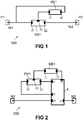
- FIG. 1 shows a semiconductor device 100 comprising a magnetoelectric transducer structure ME1 operatively connected to an electrical switch SW1.
- the electrical switch SW1 has a first terminal 21 and a second terminal 22 which are to be substantially electrically connected or substantially electrically disconnected from each other.
- the electrical switch SW1 further comprises a third terminal, also referred to as control terminal 23 for controlling the state of the switch.
- the switch SW1 has two main states or main modes of operation: open or closed.
- the magnetoelectric transducer ME1 is adapted for providing a voltage signal to said third terminal 23 of the switch SW1 when the external magnetic field (and hence also the magnetic field in close vicinity of ME1) changes, e.g. when the amplitude of the magnetic field increases, for example when a permanent magnet has approached the device.
- Any known magnetoelectric transducer known in the art can be used in devices of the present invention, but a few preferred embodiments of such a structure will be described further, in particular when discussing FIG. 3 to FIG. 14 and FIG. 21 to FIG. 23 .
- the first terminal 21 of the switch SW1 is connected to a first node N1 of a semiconductor device, which can be an internal node or can be connected to an external pin P1 of the semiconductor device.
- the second terminal 22 of the switch SW1 is connected to a second node N2 of the semiconductor device, which can be an internal node or can be connected to an external pin P2.
- the device 100 can be used to replace reed switches.
- the electrical switch SW1 is a Field Effect Transistor, known as FET, providing an electrically resistive path between the first terminal 21 and the second terminal 22.
- the electrical resistance of said path depends on the voltage applied to the control terminal 23.
- the resistance is either zero or infinitely high, but in practice of course the resistance is "relatively low", e.g. lower than a predefined resistance value (for example lower than 1000 ohm or lower than 500 ohm or lower than 250 ohm) when the switch SW1 is in a state called “closed”, and the resistance value is "relatively large”, e.g. larger than the predefined resistance value (for example larger than 1000 ohm or larger than 2000 ohm or larger than 4000 ohm) when the switch SW1 is in a state called "open".
- the predefined resistance value can for example be 1000 Ohm, thus allowing a current of 1 mA when a voltage difference of 1 V is present over the two nodes N1, N2.
- the predefined resistance value can for example be 1000 Ohm, thus allowing a current of 1 mA when a voltage difference of 1 V is present over the two nodes N1, N2.
- silicon there is about a factor of 8 magnitudes between the current flowing in the "open” and the "closed” state, for example about 1 mA in open state and about 10 pA in closed state.
- a latent current of 10 ⁇ A or 10 pA makes a huge difference in terms of battery life).
- switch SW1 being a FET
- the first and second terminal 21, 22 are called “source” and “drain”
- the control terminal 23 is called “gate”.
- Any known or yet unknown type of FET can be used in embodiments of the present invention, for example: any FET selected from the group consisting of JFET, MOSFET, MNOS, DGMOSFET, DEPFET, FREDFET, HIGFET, MODFET, TFET, IGBT, HEMT, ISFET, MESFET, NOMFET, GNRFET, VeSFET, CNTFET, OFET, QFET.
- An important aspect of the present invention is the use of a magnetoelectric structure for controlling a FET, which is not a trivial combination, inter alia because it cannot be readily predicted that the voltage generated by such a structure is sufficiently high for reliably controlling the FET.
- the inventors have found that by using a stack having suitable dimensions and made of suitable materials, a sufficient amount of charge (and thus voltage) can be generated to reliably control the FET, even with magnetic field strengths in the order of a few milliTesla. More specifically, by using sufficiently thick layers (e.g. at least 1.0 or at least 2.0 ⁇ m or at least 4.0 ⁇ m thick), and sufficiently large structures (e.g. at least 0.1 mm 2 ), and by using materials having high magnetostrictive (e.g. at least 100 ppm or at least 200 ppm) or high piezoelectric properties (e.g. at least 0.5 C/m 2 or at least 1 C/m 2 ).
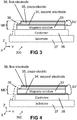
- FIG. 2 shows a semiconductor device 200 as another particular embodiment of the present invention.
- the device 200 comprises a magnetoelectric element ME1 and a switch SW1, and an additional circuitry 4.
- the additional circuitry 4 may contain only passive components such as for example one or more components selected from the group consisting of: resistors, capacitors, diodes, or may furthermore contain active components, such as transistors.
- the additional circuit 4 is arranged between the first and second node N1, N2, (which as mentioned above can be internal nodes or can be connected to external pins), but in other embodiments of the present invention, the additional circuit may be arranged between the passive magnetoelectric transducer ME1 and the control terminal 23 of the switch SW1. As can be seen, no voltage supply other than the voltage created by the magnetoelectric element ME1 is used to energize the additional circuitry 4.
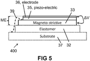
- FIG. 3 shows a material stack 300 as can be used in embodiments of the present invention.
- the stack forms a passive MagnetoElectric transducer structure "ME" mounted on a carrier.
- the carrier may furthermore comprise the switch SW1 (not shown in FIG. 3 ), although that is not absolutely required, and the switch SW1 may also be located on another substrate.
- the stack comprises:
- This stack should be flexibly mounted to a substrate 37, for example by means of an elastomer, such as PDMS or polyimide.
- the magnetostrictive element 33 compresses in a particular direction (as will be explained in FIG. 6 and FIG. 7 ), thereby exerting mechanical stress on the piezoelectric layer 35.
- this voltage ⁇ V an be applied directly or indirectly to the gate 23 of a FET to function as a switch SW1.
- AlScN is used as the piezoelectric layer
- Pt or Co is used as the material of the first electrode 36.
- the AlScN layer can be grown on top of the Pt or Mo layer.
- 50Fe50Co is used as the magnetostrictive material.
- This alloy 50Fe50Co has good properties to support the application, e.g. high initial permeability (mu>1000) and low coercivity ( ⁇ 500 A/m or ⁇ 600 ⁇ T) which reduces or minimizes the lag of electrical potential on the output versus the applied magnetic field, assuring that also small magnetic field changes (of about 1 mT) can be detected.
- This alloy has a high spontaneous magnetisation (in the order of about 2.1 T) allowing a broad working region until saturation (depending on the shape) and it has an acceptable magnetostriction (in the order of about 200 ppm) to generate enough strain/stress on the piezoelectrical layer.
- the magnetostrictive layer 33 is intimately mechanically coupled to a piezoelectric layer 35 to allow mechanical deformation (as will be shown in more detail in FIG. 7 ).
- the first and the second electrode layer 36, 34 are relatively thin in comparison with the thickness of the piezoelectric layer 35.
- each layer has a thickness in the range from 0.2 to 6.0 ⁇ m, for example in the range from 1.0 to 5.0 ⁇ m, for example equal to about 2 ⁇ m.
- the ME stack forming the magnetoelectric transducer is flexibly mounted to a substrate or carrier 37 via an elastic material, preferably a highly elastic material, e.g. a material having an E-modulus of about 0.0 to about 5.0 GPa, or an E-modulus in the range from 0.1 to 5.0 GPa, or an E-modules in the range from 0.5 to 5.0 GPa), for example an elastomer 38 such as for example polyimide or PDMS.
- an elastic material preferably a highly elastic material, e.g. a material having an E-modulus of about 0.0 to about 5.0 GPa, or an E-modulus in the range from 0.1 to 5.0 GPa, or an E-modules in the range from 0.5 to 5.0 GPa
- an elastomer 38 such as for example polyimide or PDMS.
- the ME-stack (and in particular the magnetostrictive material and the piezoelectrical material) to deform in the presence of a magnetic field without the need to mount the ME stack on a cantilever which is suspended at one end thereof, for example.
- the ME stack according to the present invention is also more robust against mechanical shocks, since such cantilevers can break.
- the carrier is a semiconductor substrate 37 further comprising the semiconductor switch SW1 embedded therein.
- the substrate 37 may be a CMOS substrate with the FET embedded therein, and further comprising conductive tracks for allowing interconnection with the electrodes 34, 36, for example via bondpads (not shown), in classical manners.
- the magnetostrictive layer 33 is typically one single layer of the stack. This single layer 33 may comprise one single zone or region (as shown in FIG. 12 ), or may comprise at least two separate zones or regions, as will be explained further when discussing FIG. 13 and FIG. 14 .
- the ME stack may be completely covered by another PDMS layer (not shown in FIG. 3 ), assuring decoupling from the package stress.
- the ME stack may be partly covered by an elastomer layer 92 at a major portion of its surface, but be in direct contact with the chip package (e.g. with a mould compound 93) at specific positions, as will be explained further in FIG. 9 or FIG. 10 .
- using separate structures may allow to reduce or reject package stress and/or thermal stress.
- FIG. 4 shows a material stack 350 similar to that of FIG. 3 , except that the electrodes 34, 36 are located on opposite sides of the magnetostrictive layer 33.
- the magnetostrictive layer 33 is located between the two electrode layers 34, 36, but the working principles of the magnetoelectric stack are the same: when a magnetic field is applied, a voltage is generated over the electrodes by the interaction between the magnetostrictive and piezoelectric layer, and when the magnetic field is removed or disappears, the voltage also disappears. This voltage is used to open or close a switch SW1, resulting in a "passive magnetic switch".
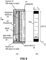
- FIG. 5 shows a material stack 400 similar to that of FIG. 3 , except that the second electrode layer 34 between the magnetostrictive layer 33 and the piezoelectric layer 35 is omitted, and that the magnetostrictive layer 34 itself is electrically conductive, and functions as second electrode. Everything else described above for the stack 300 is also applicable here.
- the stack 400 is easier to produce than the stack 300 of FIG. 3 and the stack 350 of FIG. 4 .
- Suitable materials for the magnetostrictive layer are for example: NiFe, FeTb, FeGa, terfenol, FeCo.
- FIG. 6 shows an example of a magnetostrictive layer 33 having a rectangular shape, when seen in top view. This rectangle is also referred to herein as “magnetostrictive element” 33.
- FIG. 6(a) shows that the magnetostrictive element has a preferential magnetization along the X axis, even in the absence of an external magnetic field Bext. This behaviour is not obtained automatically, but can be created by annealing the magnetostrictive material in the presence of a constant magnetic field oriented parallel with the X-axis (see step 1906 and/or step 1923 in FIG. 21 ) during the production stage.
- the ratio of the length L1 and the width W1 is a value in the range from 2 to 200, for example a value in the range from 2 to 20, for example equal to about 5 or equal to about 10.
- FIG. 6(b) shows the magnetostrictive element 33 of FIG. 6(a) in the presence of an external magnetic field Bext oriented in the Y-direction, or at least having a non-zero component along the Y axis, as can be achieved for example by approaching the ME stack with a permanent magnet. Assuming the magnetostriction is negative, then such approach causes a contraction of the magnetostrictive element 33 along the Y axis, and an expansion of the material along the X axis and a contraction in the Z-axis The main effect in X and Y direction are caused by the magnetostriction effects.
- FIG. 7 shows the magnetostrictive element 33 of FIG. 6 in side view, with a piezoelectric element 35 and an electrode 36 of the same length and width on top, forming the magnetoelectric element 73a. It is assumed in this example that the magnetostrictive material is conductive, and that the layer 33a is electrically conductive, hence functions also as the second electrode. Otherwise, a second electrode layer can also be added (not shown), as explained in FIG. 5 .
- FIG. 7(a) shows the magnetostrictive stack 73a in the absence of a magnetic field Bext.
- FIG. 7(b) shows the stack of FIG. 7(a) in the presence of a magnetic field having a component along the Y axis, causing a contraction of the magnetostrictive material 33b along the Y axis, further causing a contraction in the Y-direction of the piezoelectric element 35b mounted thereon and intimately connected thereto.
- This mechanical deformation causes a voltage to be generated between the electrodes.
- a magnetostrictive material with a negative magnetostriction was used, a magnetic field with a component in the Y-direction would cause a contraction in the Y-direction, and an expansion in the X-direction.
- a magnetostrictive material with a positive magnetostriction was used, a magnetic field with a component in the Y-direction would cause an expansion in the Y-direction and a contraction in the X-direction, but in both cases, a voltage would be generated by the piezoelectric layer.
- FIG. 8 shows a variant of the structure of FIG. 6(a) , wherein the magnetostrictive element 33 has a U-shape or a bridge shape, and wherein opposite sides of the magnetostrictive layer are directly connected to the substrate 37 to prevent or at least reduce mechanical contraction in the Y-direction.
- the magnetostrictive strip 33 of FIG. 8 is an elongated strip, which is fixed at opposite ends to the substrate 37 in a non-elastic manner.
- the location where the magnetostrictive strip 33 is in direct contact with the substrate is indicated by a thick black line in FIG. 8(a) for illustrative purposes.
- This asymmetric connection has the effect that, as the material movement is restricted in the Y direction, there is a tensile stress arising in Y-direction (when a magnetic field is applied) which causes the thickness (and the width) of the magnetostrictive layer 33 to decrease and a polarisation to arise on the piezoelectrical layer.
- the electrode layer(s) is/are not explicitly shown in FIG.
- the piezoelectric layer is in intimate contact with the magnetostrictive layer 33 in a similar manner as shown in FIG. 3 and FIG. 4 . Since the piezo-electric layer is grown, the axis of the crystal is preferably pointing as much as possible toward the polarization axis, perpendicular to the electrode(s).
- FIG. 9(a) shows a variant of the structure of FIG. 8 , wherein the magnetostrictive strip 33 is also fixed at two ends thereof, but not to the substrate, but to the package 93, e.g. made of plastic molding compound.
- the magnetostrictive strip 33 it would also be possible to connect the magnetostrictive strip 33 both to the substrate and to the package. The same effect as described above (in FIG. 8 ) also occurs here.
- FIG. 9(b) shows a view on the structure of FIG. 9(a) as seen in the direction indicated by arrow "A", if the molding compound 93 would not be present.
- the contact area between the magnetostrictive material and the molding compound is indicated by two black lines in FIG. 9(a) and two black surfaces in FIG. 9(b) , for illustrative purposes only.
- FIG. 10 is a variant of the structure of FIG. 9 , where the position of the magnetostrictive layer and the piezo-electric layer are swapped, and wherein the piezo-electric layer is fixed to the mold.
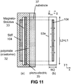
- FIG. 11 is another variant of the structure of FIG. 8 , where a stiff elongated element (different from the substrate and different from the package) is mechanically connected to the magnetostrictive strip, e.g. deposited thereon.
- stiff is meant that the E-modulus of the elongated element is at least a factor 1.20 higher than the E-modules of the magnetostrictive material, for example at least a factor 1.50 or at least a factor 2.0.
- This has the effect that the structure has a higher mechanical stiffness (i.e. has a higher Young-modules) in the longitudinal direction of the elongated element, and a smaller mechanical stiffness (i.e. has a smaller E-modulus) in a transverse direction.
- the elongated material can for example be made of a material selected from the group consisting of copper, gold, platinum, molybdenum, nickel, but the present invention is not limited hereto, and other suitable metal or metal alloy, or even the piezoelectrical-material itself may be used, provided it has a higher stiffness than the magnetostrictive material.
- the "stiff element” is a small zone of the substrate 37, which can be made by making an elongated opening in the elastomer layer 32 before depositing magnetostrictive material on top of said elastomer layer.
- the stiff element 104 on the opposite side of the magnetostrictive layer 33 can be omitted.
- both the stiff elongated element 104 is present, and the magnetostrictive layer 33 is in direct contact with the substrate 37 over a relatively narrow elongated zone. This reduces the material movement in the Y-direction even more.
- FIG. 12 shows an example of a passive magnetoelectric transducer structure "ME1" comprising a plurality of "N" magnetoelectric rectangular elements 1101, 1102, etc., as can be used in embodiments of the present invention.
- the magnetoelectric elements are connected electrically in series, i.e. the first electrode 36 of one element is connected to the second electrode 34 of an adjacent element, etc., so as to form a chain.
- the total voltage between the nodes N1 and N2 thus obtained is substantially equal to the number of elements N multiplied by the individual voltage. In this way the gate voltage of the switch SW1 can be further increased.
- FIG. 13 shows an example of a device 1200 comprising:
- ME1 When implemented on a single die, ME1 can for example be magnetized in the X-direction and ME2 in the Y-direction by rotational magnetic field annealing, where magnetization will attain the longest direction. Another solution is to anneal in the presence of a magnetic field oriented at 45° relative to the X- and Y-axis. Yet another solution is to implement the first and second magnetoelectric structures ME1 and ME2 on different dies, and combining them.
- the structure 33x and 33y are shown at 90°, that is not absolutely required, and another angle in the range from 45° to 135°, or from 75° to 105° could also be used.
- magnetisation at such as small scale can be achieved for example by applying a magnetic concentrator before or during annealing, which magnetic concentrator is stripped afterwards.
- annealing can be performed in a rotating magnetic field, in which case the induced magnetisation will be along the long side of the structure, since during the annealing the magnetisation will tend towards the long axis.
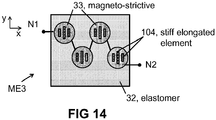
- FIG. 14 shows another example of a passive magnetoelectric transducer structure ME3, which can be seen as a variant of the magnetoelectric transducer structure of FIG. 12 , but using one or more "stiff elongated elements" located on top of or underneath the magnetostrictive layer 33, but in direct mechanical contact thereto, as discussed and illustrated in relation to FIG. 11 .
- FIG. 15 is an exemplary block diagram of a device 1400 comprising for example the first and a second transducer structure shown in FIG. 13 , represented by their equivalent electrical circuit comprising a voltage source ⁇ V1, ⁇ V2 in series with a capacitance C1, C2, the latter being related to the first and second electrode 36, 34 being arranged at a small distance.
- a voltage source ⁇ V1, ⁇ V2 in series with a capacitance C1, C2, the latter being related to the first and second electrode 36, 34 being arranged at a small distance.
- an indication "(Bx)" and “(By)” is provided to indicate for which magnetic field component each "voltage source" is sensitive.
- the device 1400 further comprises four diodes D1-D4, arranged to function as a rectifier circuit.
- the four diodes are preferably embedded in the same substrate where the FET is preferably embedded, for example a CMOS substrate.
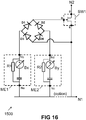
- FIG. 16 shows a block-diagram of a device 1500, which can be seen as a variant of the circuit of FIG. 15 , further comprising two resistors R1, R2 for deliberately discharging the first and second magnetoelectric transducer structure ME1, ME2.
- the circuit of FIG. 16 is used as a passive "wake-up circuit" for an application, which for example only gets power when the first switch SW1 is closed, for example from an external power supply, e.g. from a battery (not shown), that application can for example provide additional circuitry for "taking over” via another switch (not shown), so that the actual circuit receives sufficient power for doing its task.
- the application can for example disconnect its local switch, and wait until it is woken-up the next time by the circuit shown in FIG. 16 .
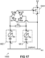
- FIG. 17 shows a block-diagram of a device 1600, which can be seen as a variant of the circuit of FIG. 16 , not comprising R1 and R2, but comprising R3 instead.
- the resistor R3 is connected between node Nb of the first magnetoelectric transducer ME1 and node Nd of the second magnetoelectric transducer ME2, and is also provided for the purpose of discharging the circuit. Again, depending on the value of R3, the discharge can happen relatively fast or relatively slow. The skilled person can find suitable values for R3 depending on the application.
- the nodes Na and Nc are interconnected, and are optionally but not necessarily connected to node N1. As shown in FIG. 18 , the nodes Na and Nc may also be connected to each other, but left floating. The latter offers the advantage of temperature compensation, because both voltage sources would provide a same or similar charge increase due to temperature variations.
- FIG. 18 shows a block-diagram of a device 1700 that furthermore comprises a state-machine 1721 and a second switch SW2, and optional further resistors 1722, 1723.
- the state-machine 1721 may for example implement a count-down counter counting at a predefined clock frequency when active, and may be adapted for being preset and keeping the switch SW2 open when the circuit 1721 wakes up when the first switch SW1 is being closed, and adapted for counting down subsequently, and for closing the switch SW2 when the counter reaches a predetermined value, e.g. zero, thereby connecting the gate "G" of the first switch SW1 to the source “S” of the first switch SW1 to open the switch SW1.
- a predetermined value e.g. zero
- the switch SW1 can be opened a predefined time after being closed, without having to rely on an RC-constant.
- the switch SW2 is closed, the capacitors C1 and C2 of the magnetoelectric stacks are also discharged.
- Resistor R3 is optional.
- FIG. 19 a structure as shown in FIG. 19 , comprising a single MagnetoElectric structure ME can also be used.
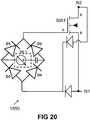
- FIG. 20 shows a variant of the circuit of FIG. 19 having two additional diodes.
- FIG. 21 is a flowchart illustrating a method 1900 of making a device according to the present invention. The method comprises three groups of steps.
- the first group of steps, group 1900A comprises the steps of:
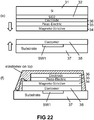
- FIG. 22(b) shows an example of a stack 2000A produced by this sequence of steps.
- the method 1900 may further comprise the optional step 1906 of annealing the stack 2000A in the presence of a constant magnetic field oriented in the X-axis.
- the method 1900 may further comprise an optional step 1907 of coating the stack with an elastomer.
- the stack can be further shaped or structured after bonding.
- the second group of steps, group 1900B comprises the steps of:
- FIG. 22(d) shows an example of a substrate 2000B produced by this sequence of steps.
- the third group of steps, group 1900C comprises the steps of:
- FIG. 22(e) and (f) illustrate the result of these steps.
- One or both of the annealing steps 1906 and/or 1923 may be present.
- At least one of the coating steps 1907 and/or 1911 is required.
- the method 1900 may further include one or more of the following steps:
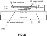
- FIG. 23 shows a structure where a switch (e.g. a FET) and the magnetoelectrical transducer structure are integrated on a single substrate.
- a switch e.g. a FET
- the magnetoelectrical transducer structure are integrated on a single substrate.
- this device 2100 comprises a substrate 37; an elastomer layer 38 on top of the substrate; a second electrode 34 on top of the elastomer layer 38, made of n-GaN channel; a piezoelectric layer, in the example comprising AlGaN; a first electrode 36 on top of the piezoelectric layer 35, made of p-GaN channel; and a magnetostrictive layer 33, made of CoFe, preferably 50% Co and 50% Fe.
- another elastomer layer may be deposited on top of the entire structure for reducing packaging stress.
Landscapes
- Engineering & Computer Science (AREA)
- Manufacturing & Machinery (AREA)
- Hall/Mr Elements (AREA)
Abstract
Description
- The present invention relates to the field of semiconductor devices comprising a passive magnetoelectric transducer structure, and to the field of passive magnetic switches.
- Devices for detecting the presence of a magnetic field are known in the art. Well known examples are: a reed switch as an example of a discrete mechanical component, and a Hall element as an example of a component embedded in an integrated semiconductor device.
- The reed switch, invented in 1936, is an electrical switch operated by an applied magnetic field. It consists of a pair of contacts of ferrous metal reeds in a hermetically sealed glass envelope. The contacts may be normally open but closing when a magnetic field is present, or normally closed and opening when a magnetic field is applied. The switch may be actuated by a coil, making a reed relay, or by bringing a magnet near to the switch. Once the magnet is pulled away from the switch, the reed switch will go back to its original position. Reed switches are used for example as a proximity switch for a burglar alarm. The technology for making reed switches is very mature, but as such they cannot be integrated in semiconductor devices. A major advantage of reed switches is that they are passive devices, meaning that they do not require electrical energy for sensing the presence of a magnetic field.
- Hall elements are well known integrated devices for sensing a magnetic field. Hall elements typically have four nodes: two energising nodes and two sensing nodes. When a constant voltage or a constant current is applied over the energising nodes, the strength of the magnetic field can be measured as a differential voltage over the sensing nodes. A disadvantage of Hall elements is that they require electrical energy.
- It is an object of embodiments of the present invention to provide a semiconductor device comprising a magnetoelectric transducer structure, and to a method of making such a device, and to the use of such a magnetoelectric transducer structure.
- It is an object of particular embodiments of the present invention to provide a passive magnetic switch.
- These and other objectives are accomplished by a semiconductor device and a method of producing such a semiconductor device according to embodiments of the present invention.
- In a first aspect, the present invention provides a semiconductor device comprising: a passive magnetoelectric transducer structure adapted for generating a charge caused by mechanical stress induced by a magnetic field.
- In an embodiment, the semiconductor device further comprises a semiconductor switch electrically connected to said passive magnetoelectric structure, the switch having a first terminal and a second terminal and a control terminal, the switch being adapted for selectively electrically connecting and disconnecting the first and second terminal depending on a signal presented at the control terminal; the transducer structure having a first terminal electrically connected to the control terminal of the switch, and having a second terminal electrically connected to the first terminal of the switch, and being adapted for opening or closing the switch.
- It is noted that "electrically connected to the control terminal" can mean a direct connection, or an indirect connection, for example via a passive subcircuit such as for example a rectifier circuit or a differential bridge circuit, e.g. a Wheatstone-bridge, or the like.
- The passive transducer structure may comprise or may be a piezoelectric material.
- It is an advantage of this structure that it allows to make a passive switch, capable of opening or closing the switch without requiring energy from for example a battery.
- The switch may be a component that provides an electrical path with a variable resistance, depending on the control signal. When the resistance value is lower than a predefined resistance value, e.g. lower than 1000 Ohm, the switch is considered to be "closed". When the resistance value is higher than said predefined number, the switch is considered to be "open".
- In an embodiment, the semiconductor switch is a Field Effect Transistor having a gate being the control terminal, and a source being the first terminal, and a drain being the second terminal, or the semiconductor switch is a Field Effect Transistor having a gate being the control terminal, and a source being the second terminal, and a drain being the first terminal.
- When the voltage of the gate is sufficiently higher than the voltage of the source, or sufficiently lower than the voltage of the drain, the transistor is switched "ON", i.e. a low resistive electrical path is formed between the source and the drain, or in other words, the switch is "closed".
- The FET may be selected from the group consisting of JFET, MOSFET, MNOS, DGMOSFET, DEPFET, FREDFET, HIGFET, MODFET, TFET, IGBT, HEMT, ISFET, MESFET, NOMFET, GNRFET, VeSFET, CNTFET, OFET, QFET.
- In an embodiment, the magnetoelectric transducer structure is mounted to a substrate or arranged inside a package in such a way that the magnetoelectric transducer structure has a first stiffness or first E-modulus in a first direction, and a second stiffness or a second E-modulus in a second direction perpendicular to the first direction, different from the first stiffness or first E-modulus.
- In an embodiment, the ratio of the first and second E-modulus is smaller than 90% or larger than 110%, for example smaller than 80% or larger than 120%, for example less than 70% or larger than 130%.
- In an embodiment, the first and second stiffness is defined by the size and/or geometry of the magnetoelectric layer having a non-constant thickness and/or a non-uniform shape, or because the magnetoelectric layer is fixedly connected or mounted to or comprises a non-flexible elongated element.
- It is an advantage of such a structure that it has a different "stiffness" in different directions parallel to the substrate. In other words, in these embodiments, the magnetoelectric transducer structure is mounted in a particular way so as to cause an asymmetrical stiffness. This allows to induce a polarization in a direction (Z) perpendicular to the plane of the substrate causing a voltage difference between the top and bottom surface, and an opposite charge on both surfaces of the piezoelectric layer.
- In an embodiment, the magnetoelectric transducer structure is connected to a substrate by means of an elastic connection over a major portion of its surface area, and by means of an elongated strip having a length over width ratio of at least 2.0 over a minor portion of of its surface area.
- In an embodiment, the magnetoelectric transducer structure is flexibly mounted to a substrate over a central portion of the transducer structure and fixedly connected to the substrate on at least two distinct locations for reducing mechanical expansion or contraction of the transducer structure between these locations when a magnetic field is applied.
- In an embodiment, the magnetoelectric transducer structure is flexibly mounted to a package over a central portion of the transducer structure and fixedly connected to the package on at least two distinct locations for reducing mechanical expansion or contraction of the transducer structure between these locations when a magnetic field is applied.
- In an embodiment, the semiconductor device further comprises an elongated element having a stiffness or an E-modulus higher than that of the magnetoelectric transducer structure, which elongated element is mounted to the transducer structure (ME) on at least two distinct locations for reducing mechanical expansion or contraction of the transducer structure between these locations when a magnetic field is applied.
- These are a few specific examples of ways how a magnetoelectric transducer structure with an asymmetric stiffness can be provided, as will be illustrated for example in
FIG. 8 to FIG. 11 . - In an embodiment, the passive magnetoelectric transducer structure comprises a magnetostrictive layer intimately mechanically coupled to a piezoelectric layer or piezoelectric element.
- Optionally the piezoelectric layer or piezoelectric element comprises a piezoelectric material selected from the group consisting of AIN, ZnO, AIScN, PZT and AlGaN.
- Optionally the piezoelectric layer comprises an elongated element having a stiffness or an E-modulus higher than that of the magnetoelectric transducer structure for reducing mechanical expansion or contraction of the piezoelectric layer in the longitudinal direction of the elongated element when a magnetic field is applied.
- Optionally the magnetostrictive layer comprises a magnetostrictive material selected from the group consisting of FeGa, FeCo, FeTb, FeCoSiB and FeCoB.
- In an embodiment the passive magnetoelectric transducer structure comprises a piezoelectric film with embedded magnetostrictive powder. The piezoelectric film with embedded magnetostrictive powder has a preferential magnetization along a first axis in the absence of an external magnetic field.
- In case the magnetostrictive material is a layer, it is preferred that the piezoelectric material is oriented such that the axis corresponding to the highest piezoelectric constant is substantially perpendicular to that the plane of the magnetostrictive layer. The preferential magnetisation of the magnetostrictive layer is typically parallel to the plane of the magnetostrictive layer.
- In an embodiment, the piezoelectric element comprises a piezoelectric material selected from the group consisting of AlN, ZnO and AlScN.
- The piezoelectric element may have a rectangular shape with a length (L) and a width (W), where a ratio of the length and the width is a value in the range from 2 to 100.
- In an embodiment, the magnetostrictive layer comprises a magnetostrictive material selected from the group consisting of FeGa and FeCo.
- In an embodiment, the first magnetostrictive material has a preferential magnetization along a first axis (e.g. X) in the absence of an external magnetic field.
- In an embodiment, the passive magnetoelectric transducer structure comprises a plurality of at least two piezoelectric elements electrically connected in series and oriented in parallel with each other.
- The series connection provides a larger signal for controlling the switch, thus the resistance of the switch is typically lower, and the control is more reliable.
- Preferably each of the piezoelectric elements has a Length over Width ratio in the range from 2 to 100, for example in the range from 2 to 10, for example a L/W of about 5.
- In an embodiment, the semiconductor device further comprises a second passive magnetoelectrical transducer structure comprising a second magnetostrictive layer intimately mechanically coupled to at least one second piezoelectric element, the second magnetostrictive layer comprising a second magnetostrictive material; and the second magnetostrictive material has a preferential magnetization along a second axis (e.g. Y) different from the first axis (e.g. X) in the absence of an external magnetic field.
- The second magnetostrictive material can be the same or a different material from the first magnetostrictive material, but is preferably the same material. However, the second magnetostrictive layer is preferably physically separated from the first magnetostrictive layer, because it has a preferential magnetization along a different axis.
- In an embodiment, the semiconductor device comprises a first magnetoelectrical stack comprising a first magnetostrictive material having a positive magnetostriction, and comprises a second magnetoelectrical stack comprising a second magnetostrictive material having a negative magnetostriction, and the first and the second magnetoelectrical stack being connected in series and being oriented so as to have different directions of maximum sensitivity.
- In this way (unwanted) thermal sensitivity of the semiconductor device can be reduced.
- The first and second magnetoelectrical stack may each contain a plurality of elongated strips, and the strips of the first stack may be oriented perpendicular to the strips of the second stack.
- In an embodiment, the second passive magnetostrictive transducer structure comprises a plurality of at least two piezoelectrical elements electrically connected in series, each of these piezoelectrical elements being intimately mechanically coupled to the second magnetostrictive layer and being oriented in parallel with respect to each other, for providing a second voltage signal; and the device further comprises a passive electrical circuit for generating a differential signal between the first control signal and the second control signal.
- The series connection provides a larger signal for controlling the switch, thus the resistance of the switch is typically lower, and the control is more reliable.
- It is an advantage of the structure that provides two separate signals related to magnetic field components in two different directions, because this allows to use a differential signal between the signal obtained from the first magnetoelectrical structure and the signal obtained from the second magnetoelectrical structure, which is less sensitive to temperature, which makes the circuit suitable for automotive applications.
- The passive electrical circuit can for example comprise one or more rectifier circuits, or a differential bridge circuit, e.g. a Wheatstone-bridge circuit.
- It is an advantage to use the differential charge or voltage created by two magnetoelectric stacks that are sensitive to different magnetic stimuli Bx, By, in order to avoid charge generation by temperature changes or other stray effects.
- In an embodiment, the first switch is embedded in a semiconductor substrate; and the substrate further comprises an elastomer layer; and the first passive magnetoelectric transducer structure is mounted to the elastomer layer such that the magnetostrictive layer is facing the elastomer layer.
- The magnetostrictive layer may be in physical contact with the elastomer layer.
- The substrate may be a silicon substrate, and/or the elastomer layer may comprise or consist of PDMS or polyimide.
- In an embodiment, the semiconductor device furthermore comprises a state machine adapted for actively resetting the voltage over the magnetoelectric structure after a predefined time after a trigger event.
- In a second aspect, the present invention provides a method of producing a semiconductor device according to the first aspect, comprising the steps of: providing a silicon substrate comprising an oxide layer on top of said silicon substrate; providing a first electrode layer on top of said oxide layer; providing a piezoelectric and magnetostrictive layer or structure; optionally annealing the first substrate in the presence of a constant magnetic field; providing a second substrate comprising at least one semiconductor switch having a first terminal and a second terminal and a control terminal; providing an elastomer layer on top of the second substrate; mounting the first substrate to the second substrate such that the piezoelectric and magnetostrictive layer or structure is facing the elastomer layer; removing the silicon and the silicon oxide layer of the first substrate; electrically connecting the first electrode to the first terminal of the switch, and electrically connecting the second electrode to the control terminal of the switch.
- In an embodiment, the step of providing the piezoelectric and magnetostrictive layer or structure comprises the steps of: i) providing a piezoelectric layer on top of said first electrode layer; ii) optionally providing a second electrode layer on top of the piezoelectric layer; iii) providing a magnetostrictive layer on top of the second electrode or directly on top of the piezoelectric layer.
- In an embodiment, the step of providing the piezoelectric and magnetostrictive layer or structure comprises the step of: iv) providing a piezoelectric layer comprising magnetostrictive powder, on top of said first electrode layer.
- The method may further comprise a step of providing an elongated strip on top of the magnetostrictive layer, such that the elongated strip is directly connected to the magnetostrictive layer on at least two distinct locations.
- The method may further comprise a step of providing two spaced openings (holes) or an elongated slot in the elastomer layer for connecting the magnetostrictive layer via said openings or via said slot to the substrate.
- In a third aspect, the present invention relates to the use of a passive magnetoelectric transducer structure as specified in the first aspect, for creating an input signal for opening or closing an electrical switch, in particular an integrated semiconductor switch, without the need for an external power supply.
- The present invention also relates to the use of a device according to the first aspect as a passive wake-up circuit for passing or blocking power to a second circuit.
- The switch would typically be arranged in series with a supply voltage, and the wake-up circuit would connect the supply voltage to the second circuit (e.g. a metering device) when a magnetic field is applied to or approaches the device.
- Particular and preferred aspects of the invention are set out in the accompanying independent and dependent claims. Features from the dependent claims may be combined with features of the independent claims and with features of other dependent claims as appropriate and not merely as explicitly set out in the claims.
- These and other aspects of the invention will be apparent from and elucidated with reference to the embodiment(s) described hereinafter.
-
-
FIG. 1 shows an embodiment of a semiconductor device according to the present invention. The device comprises a magnetoelectric transducer structure or element and optionally a switch. -
FIG. 2 shows another embodiment of a semiconductor device according to the present invention. The device comprises a magnetoelectric element and optionally a switch, and optionally additional circuitry. -
FIG. 3 shows an example of a material stack as can be used in embodiments of the present invention, comprising a magnetostrictive element (or layer) and a piezoelectrical element (or layer) and two additional electrodes. In this embodiment, both electrodes are located on the same (upper) side of the magnetostrictive layer. -
FIG. 4 shows a variant of the semiconductor stack ofFIG. 3 as can be used in embodiments of the present invention. In this embodiment, the electrodes are located on opposite sides of the magnetostrictive layer, or in other words, the magnetostrictive layer is located between the two electrodes. -
FIG. 5 shows another semiconductor stack as can be used in embodiments of the present invention, comprising a magnetostrictive element (or layer) and a piezoelectrical element (or layer) and only one additional (first) electrode, the magnetostrictive element forming the other (second) electrode. -
FIG. 6 shows an example of a magnetostrictive element in top view. -
FIG. 6(a) shows that the magnetostrictive material has a preferential magnetization along the X axis, even in the absence of an external magnetic field. -
FIG. 6(b) shows a magnetostrictive material with negative magnetostriction in the presence of a magnetic field having a component By along the Y axis, causing a contraction of the magnetostrictive material along the Y axis, and an expansion of the material along the X axis and the Z-axis. -
FIG. 7 shows the magnetostrictive elements ofFIG. 6 in side view, with a piezoelectric element and an electrode on top. -
FIG. 7(a) shows the stack in the absence of a magnetic field. -
FIG. 7(b) shows the stack ofFIG. 6(b) in the presence of a magnetic field having a component along the Y axis, causing a contraction of the magnetostrictive material along the Y axis, further causing a contraction of the piezoelectric element mounted thereon and intimately connected thereto (not explicitly shown inFIG. 7 but see for exampleFIG. 3 to FIG. 5 ) -
FIG. 8 shows a variant of the structure ofFIG. 6(a) , wherein the magnetostrictive strip is fixed at two ends or two sides thereof to the substrate, to mechanically prevent or at least reduce the magnetostrictive strip from shrinking in its longitudinal direction. (some layers are not shown). -
FIG. 9 is a variant of the structure ofFIG. 8 , wherein the magnetostrictive strip is fixed at two ends or two sides thereof to a mould. (some layers are not shown). -
FIG. 10 is a variant of the structure ofFIG. 9 , where the position of the magnetostrictive layer and the piezo-electric layer are swapped, and wherein the piezo-electric layer is fixed to the mold. -
FIG. 11 is another variant of the structure ofFIG. 8 , where a stiff elongated element (different from the substrate and different from the package) is connected to the magnetostrictive strip, such that the structure has a higher mechanical stiffness in the longitudinal direction of the elongated element, and a smaller mechanical stiffness in a transverse direction. -
FIG. 12 shows an example of a first passive magnetoelectric transducer structure comprising a magnetostrictive layer and a plurality of piezoelectric elements in the form of elongated strips, e.g. rectangular strips, mounted thereon, as can be used in embodiments of the present invention. -
FIG. 13 shows an example of a device according to an embodiment of the present invention. The device comprises (left ofFIG. 13 ) a first passive magnetoelectric transducer structure like the one shown inFIG. 12 where the magnetostrictive material has a preferential magnetization along the X axis, and a second passive magnetoelectric transducer structure (right ofFIG. 13 ) like the one shown inFIG. 12 , but where the magnetostrictive material has a preferential magnetization along the Y axis. -
FIG. 14 shows a variant of the structure ofFIG. 12 , where several "magnetostrictive islands with a non-uniform stiffness" are mounted on an elastomer layer, and are interconnected. -
FIG. 15 is an electrical block diagram of a device according to an embodiment of the present invention, comprising a first and a second transducer structure as illustrated inFIG. 12 or FIG. 13 , , and further comprising four diodes and a FET. -
FIG. 16 is a variant of the circuit ofFIG. 15 , further comprising two resistors for discharging the first and second magnetoelectric transducer structure. -
FIG. 17 is another variant of the circuit ofFIG. 15 , further comprising one resistor for discharging the first and second magnetoelectric transducer structure. -
FIG. 18 is another variant of the circuit ofFIG. 15 , further comprising a state-machine and a second switch. -
FIG. 19 shows another variant of the circuit ofFIG. 15 comprising only one magnetoelectric transducer structure and a switch. -
FIG. 20 shows a variant of the circuit ofFIG. 19 having two additional diodes. -
FIG. 21 is a flowchart illustrating a method of making a magnetoelectric transducer structure like to ones shown inFIG. 3 to FIG. 5 , according to an embodiment of the present invention. -
FIG. 22(a) to (f) also illustrates the method according to the present invention. -
FIG. 23 shows a structure where a switch (e.g. a FET) and the magnetoelectrical transducer structure are integrated on a single substrate. - The drawings are only schematic and are non-limiting. In the drawings, the size of some of the elements may be exaggerated and not drawn on scale for illustrative purposes. Any reference signs in the claims shall not be construed as limiting the scope. In the different drawings, the same reference signs refer to the same or analogous elements.
- The present invention will be described with respect to particular embodiments and with reference to certain drawings but the invention is not limited thereto but only by the claims. The drawings described are only schematic and are non-limiting. In the drawings, the size of some of the elements may be exaggerated and not drawn on scale for illustrative purposes. The dimensions and the relative dimensions do not correspond to actual reductions to practice of the invention.
- Furthermore, the terms first, second and the like in the description and in the claims, are used for distinguishing between similar elements and not necessarily for describing a sequence, either temporally, spatially, in ranking or in any other manner. It is to be understood that the terms so used are interchangeable under appropriate circumstances and that the embodiments of the invention described herein are capable of operation in other sequences than described or illustrated herein.
- Moreover, the terms top, under and the like in the description and the claims are used for descriptive purposes and not necessarily for describing relative positions. It is to be understood that the terms so used are interchangeable under appropriate circumstances and that the embodiments of the invention described herein are capable of operation in other orientations than described or illustrated herein.
- It is to be noticed that the term "comprising", used in the claims, should not be interpreted as being restricted to the means listed thereafter; it does not exclude other elements or steps. It is thus to be interpreted as specifying the presence of the stated features, integers, steps or components as referred to, but does not preclude the presence or addition of one or more other features, integers, steps or components, or groups thereof. Thus, the scope of the expression "a device comprising means A and B" should not be limited to devices consisting only of components A and B. It means that with respect to the present invention, the only relevant components of the device are A and B.
- Reference throughout this specification to "one embodiment" or "an embodiment" means that a particular feature, structure or characteristic described in connection with the embodiment is included in at least one embodiment of the present invention. Thus, appearances of the phrases "in one embodiment" or "in an embodiment" in various places throughout this specification are not necessarily all referring to the same embodiment, but may. Furthermore, the particular features, structures or characteristics may be combined in any suitable manner, as would be apparent to one of ordinary skill in the art from this disclosure, in one or more embodiments.
- Similarly it should be appreciated that in the description of exemplary embodiments of the invention, various features of the invention are sometimes grouped together in a single embodiment, figure, or description thereof for the purpose of streamlining the disclosure and aiding in the understanding of one or more of the various inventive aspects. This method of disclosure, however, is not to be interpreted as reflecting an intention that the claimed invention requires more features than are expressly recited in each claim. Rather, as the following claims reflect, inventive aspects lie in less than all features of a single foregoing disclosed embodiment. Thus, the claims following the detailed description are hereby expressly incorporated into this detailed description, with each claim standing on its own as a separate embodiment of this invention.
- Furthermore, while some embodiments described herein include some but not other features included in other embodiments, combinations of features of different embodiments are meant to be within the scope of the invention, and form different embodiments, as would be understood by those in the art. For example, in the following claims, any of the claimed embodiments can be used in any combination.
- In the description provided herein, numerous specific details are set forth. However, it is understood that embodiments of the invention may be practiced without these specific details. In other instances, well-known methods, structures and techniques have not been shown in detail in order not to obscure an understanding of this description.
- When reference is made to "magnetised along the X axis", what is meant is that, the material has a preferential magnetization as shown in
FIG. 6(a) , where, in the absence of an external magnetic field Bext, the local magnetisation vector is substantially parallel to the X axis, but can point in the positive or negative direction of the X axis. In other words there is 180° ambiguity. From large scale point of view, the net magnetisation is zero, where the local magnetisation is compensated by an inversed magnetisation in other positions. In other words, the anisotropy primarily caused by annealing under a constant magnetic field causes the local magnetisation to prefer a direction parallel to the X-axis. - In this document the terms "magnetoelectric transducer" and "magnetoelectric transducer structure" and "magnetoelectric stack" are used as synonyms. It can for example comprise a single magnetoelectric element, or a plurality of magnetoelectric elements electrically connected in series. It can for example be made of a real magnetoelectrical element, or it can be formed by a composite layer consisting of magnetostrictive grains embedded in a piezoelectrical layer, or it can consist of a single magnetostrictive layer in direct mechanical contact with a single piezoelectric layer, or it can consist of alternate layers of magnetostrictive and piezoelectrical material.
- The term "E-modulus" or "Young-modulus" mean the same. The larger the E-modulus of a material, the stiffer a material is. The smaller the E-modulus, the more flexible a material is. But stiffness can also be increased by changing the shape and/or the geometry of a structure.
- The present invention will be explained primarily for a structure having a discrete magnetostrictive layer (or film) and a discrete piezoelectric layer (or film), for ease of description, but the present invention is not limited thereto, and for example a piezoelectric layer with magnetostrictive powder embedded therein, can also be used.
-
FIG. 1 shows asemiconductor device 100 comprising a magnetoelectric transducer structure ME1 operatively connected to an electrical switch SW1. - The electrical switch SW1 has a
first terminal 21 and asecond terminal 22 which are to be substantially electrically connected or substantially electrically disconnected from each other. The electrical switch SW1 further comprises a third terminal, also referred to ascontrol terminal 23 for controlling the state of the switch. The switch SW1 has two main states or main modes of operation: open or closed. - The magnetoelectric transducer ME1 is adapted for providing a voltage signal to said
third terminal 23 of the switch SW1 when the external magnetic field (and hence also the magnetic field in close vicinity of ME1) changes, e.g. when the amplitude of the magnetic field increases, for example when a permanent magnet has approached the device. Any known magnetoelectric transducer known in the art can be used in devices of the present invention, but a few preferred embodiments of such a structure will be described further, in particular when discussingFIG. 3 to FIG. 14 andFIG. 21 to FIG. 23 . - The
first terminal 21 of the switch SW1 is connected to a first node N1 of a semiconductor device, which can be an internal node or can be connected to an external pin P1 of the semiconductor device. Likewise, thesecond terminal 22 of the switch SW1 is connected to a second node N2 of the semiconductor device, which can be an internal node or can be connected to an external pin P2. Thedevice 100 can be used to replace reed switches. - In preferred embodiments of the present invention, the electrical switch SW1 is a Field Effect Transistor, known as FET, providing an electrically resistive path between the
first terminal 21 and thesecond terminal 22. The electrical resistance of said path depends on the voltage applied to thecontrol terminal 23. Ideally the resistance is either zero or infinitely high, but in practice of course the resistance is "relatively low", e.g. lower than a predefined resistance value (for example lower than 1000 ohm or lower than 500 ohm or lower than 250 ohm) when the switch SW1 is in a state called "closed", and the resistance value is "relatively large", e.g. larger than the predefined resistance value (for example larger than 1000 ohm or larger than 2000 ohm or larger than 4000 ohm) when the switch SW1 is in a state called "open". - As an example, the predefined resistance value can for example be 1000 Ohm, thus allowing a current of 1 mA when a voltage difference of 1 V is present over the two nodes N1, N2. Basically in silicon there is about a factor of 8 magnitudes between the current flowing in the "open" and the "closed" state, for example about 1 mA in open state and about 10 pA in closed state. In battery powered applications, a latent current of 10 µA or 10 pA makes a huge difference in terms of battery life).
- Although semiconductor devices according to the present invention do not necessarily have a switch SW1, in particular a FET, the invention will be further explained for the switch SW1 being a FET, in which case the first and
second terminal control terminal 23 is called "gate". Any known or yet unknown type of FET can be used in embodiments of the present invention, for example: any FET selected from the group consisting of JFET, MOSFET, MNOS, DGMOSFET, DEPFET, FREDFET, HIGFET, MODFET, TFET, IGBT, HEMT, ISFET, MESFET, NOMFET, GNRFET, VeSFET, CNTFET, OFET, QFET. - An important aspect of the present invention is the use of a magnetoelectric structure for controlling a FET, which is not a trivial combination, inter alia because it cannot be readily predicted that the voltage generated by such a structure is sufficiently high for reliably controlling the FET. However, the inventors have found that by using a stack having suitable dimensions and made of suitable materials, a sufficient amount of charge (and thus voltage) can be generated to reliably control the FET, even with magnetic field strengths in the order of a few milliTesla. More specifically, by using sufficiently thick layers (e.g. at least 1.0 or at least 2.0 µm or at least 4.0 µm thick), and sufficiently large structures (e.g. at least 0.1 mm2), and by using materials having high magnetostrictive (e.g. at least 100 ppm or at least 200 ppm) or high piezoelectric properties (e.g. at least 0.5 C/m2 or at least 1 C/m2).
-
FIG. 2 shows asemiconductor device 200 as another particular embodiment of the present invention. Thedevice 200 comprises a magnetoelectric element ME1 and a switch SW1, and an additional circuitry 4. The additional circuitry 4 may contain only passive components such as for example one or more components selected from the group consisting of: resistors, capacitors, diodes, or may furthermore contain active components, such as transistors. - In the example shown in
FIG. 2 , the additional circuit 4 is arranged between the first and second node N1, N2, (which as mentioned above can be internal nodes or can be connected to external pins), but in other embodiments of the present invention, the additional circuit may be arranged between the passive magnetoelectric transducer ME1 and thecontrol terminal 23 of the switch SW1. As can be seen, no voltage supply other than the voltage created by the magnetoelectric element ME1 is used to energize the additional circuitry 4. -
FIG. 3 shows amaterial stack 300 as can be used in embodiments of the present invention. The stack forms a passive MagnetoElectric transducer structure "ME" mounted on a carrier. The carrier may furthermore comprise the switch SW1 (not shown inFIG. 3 ), although that is not absolutely required, and the switch SW1 may also be located on another substrate. - The stack comprises:
- a
magnetostrictive layer 33. This layer can consist of or comprise for example FeGa or FeCo; - an
electrode layer 34, referred to herein as "second electrode", on top of themagnetostrictive layer 33, for example consisting of or comprising FeCo or Mo or Pt; - a
piezoelectric layer 35 on top of theelectrode layer 34, for example consisting of or comprising AlN or ZnO or AlScN; - an
electrode layer 36, referred to herein as "first electrode", on top of thepiezoelectric layer 35, for example consisting of or comprising Pt or Mo or alloys thereof; - This stack should be flexibly mounted to a
substrate 37, for example by means of an elastomer, such as PDMS or polyimide. - When a magnetic field is applied in the vicinity of the stack, for example by approaching the
stack 300 with a permanent magnet, themagnetostrictive element 33 compresses in a particular direction (as will be explained inFIG. 6 and FIG. 7 ), thereby exerting mechanical stress on thepiezoelectric layer 35. This causes thepiezoelectric layer 35 to mechanically deform, which creates a voltage ΔV over theelectrodes piezoelectric layer 35 is sandwiched. As will be explained further, this voltage ΔV an be applied directly or indirectly to thegate 23 of a FET to function as a switch SW1. - The working principle of a "passive magnetic switch" according to the present invention is as follows: when the magnetic field is applied, the voltage ΔV is created by the
piezoelectric structure 300, and the switch SW1 "closes", meaning the FET is "ON". When the magnetic field is removed, the voltage also removes, and the switch "opens", meaning the FET is "OFF". - In case there is a pull-down resistor (see e.g.
FIG. 16 ), the gate of the switch is pulled towards a closed state when the magnetic field is removed. If there is no pull-down resistor (see e.g.FIG. 15 andFIG. 17 ), the gate "G" of the switch SW1 is not leaking and the voltage is removed when the charge is removed. - In preferred embodiments, AlScN is used as the piezoelectric layer, and Pt or Co is used as the material of the
first electrode 36. This offers the advantage that the crystal lattice of the template matches the crystallographic (002) direction of the AIScN, hence the AlScN crystal preferentially grows in the right crystal orientation to produce the optimal piezoelectrical output. During production, the AlScN layer can be grown on top of the Pt or Mo layer. - Preferably 50Fe50Co is used as the magnetostrictive material. This alloy 50Fe50Co has good properties to support the application, e.g. high initial permeability (mu>1000) and low coercivity (<500 A/m or < 600 µT) which reduces or minimizes the lag of electrical potential on the output versus the applied magnetic field, assuring that also small magnetic field changes (of about 1 mT) can be detected. This alloy has a high spontaneous magnetisation (in the order of about 2.1 T) allowing a broad working region until saturation (depending on the shape) and it has an acceptable magnetostriction (in the order of about 200 ppm) to generate enough strain/stress on the piezoelectrical layer.
- Referring back to
FIG. 3 , themagnetostrictive layer 33 is intimately mechanically coupled to apiezoelectric layer 35 to allow mechanical deformation (as will be shown in more detail inFIG. 7 ). Preferably the first and thesecond electrode layer piezoelectric layer 35. Preferably each layer has a thickness in the range from 0.2 to 6.0 µm, for example in the range from 1.0 to 5.0 µm, for example equal to about 2 µm. - The ME stack forming the magnetoelectric transducer, the stack comprising the magnetostrictive material and the piezoelectrical material and the
electrodes carrier 37 via an elastic material, preferably a highly elastic material, e.g. a material having an E-modulus of about 0.0 to about 5.0 GPa, or an E-modulus in the range from 0.1 to 5.0 GPa, or an E-modules in the range from 0.5 to 5.0 GPa), for example anelastomer 38 such as for example polyimide or PDMS. This allows the ME-stack (and in particular the magnetostrictive material and the piezoelectrical material) to deform in the presence of a magnetic field without the need to mount the ME stack on a cantilever which is suspended at one end thereof, for example. This simplifies manufacturing by reducing the number of process steps since no steps are required to form a cantilever and a cavity to allow the deformation. The ME stack according to the present invention is also more robust against mechanical shocks, since such cantilevers can break. - Preferably the carrier is a
semiconductor substrate 37 further comprising the semiconductor switch SW1 embedded therein. For example, thesubstrate 37 may be a CMOS substrate with the FET embedded therein, and further comprising conductive tracks for allowing interconnection with theelectrodes - The
magnetostrictive layer 33 is typically one single layer of the stack. Thissingle layer 33 may comprise one single zone or region (as shown inFIG. 12 ), or may comprise at least two separate zones or regions, as will be explained further when discussingFIG. 13 andFIG. 14 . The ME stack may be completely covered by another PDMS layer (not shown inFIG. 3 ), assuring decoupling from the package stress. Alternatively the ME stack may be partly covered by anelastomer layer 92 at a major portion of its surface, but be in direct contact with the chip package (e.g. with a mould compound 93) at specific positions, as will be explained further inFIG. 9 orFIG. 10 . As explained later inFIG. 16 , using separate structures may allow to reduce or reject package stress and/or thermal stress. -
FIG. 4 shows amaterial stack 350 similar to that ofFIG. 3 , except that theelectrodes magnetostrictive layer 33. Or stated in other words, themagnetostrictive layer 33 is located between the twoelectrode layers -
FIG. 5 shows amaterial stack 400 similar to that ofFIG. 3 , except that thesecond electrode layer 34 between themagnetostrictive layer 33 and thepiezoelectric layer 35 is omitted, and that themagnetostrictive layer 34 itself is electrically conductive, and functions as second electrode. Everything else described above for thestack 300 is also applicable here. Thestack 400 is easier to produce than thestack 300 ofFIG. 3 and thestack 350 ofFIG. 4 . Suitable materials for the magnetostrictive layer are for example: NiFe, FeTb, FeGa, terfenol, FeCo. -
FIG. 6 shows an example of amagnetostrictive layer 33 having a rectangular shape, when seen in top view. This rectangle is also referred to herein as "magnetostrictive element" 33. -
FIG. 6(a) shows that the magnetostrictive element has a preferential magnetization along the X axis, even in the absence of an external magnetic field Bext. This behaviour is not obtained automatically, but can be created by annealing the magnetostrictive material in the presence of a constant magnetic field oriented parallel with the X-axis (seestep 1906 and/orstep 1923 inFIG. 21 ) during the production stage. - Preferably the ratio of the length L1 and the width W1 is a value in the range from 2 to 200, for example a value in the range from 2 to 20, for example equal to about 5 or equal to about 10.
-
FIG. 6(b) shows themagnetostrictive element 33 ofFIG. 6(a) in the presence of an external magnetic field Bext oriented in the Y-direction, or at least having a non-zero component along the Y axis, as can be achieved for example by approaching the ME stack with a permanent magnet. Assuming the magnetostriction is negative, then such approach causes a contraction of themagnetostrictive element 33 along the Y axis, and an expansion of the material along the X axis and a contraction in the Z-axis The main effect in X and Y direction are caused by the magnetostriction effects. -
FIG. 7 shows themagnetostrictive element 33 ofFIG. 6 in side view, with apiezoelectric element 35 and anelectrode 36 of the same length and width on top, forming themagnetoelectric element 73a. It is assumed in this example that the magnetostrictive material is conductive, and that thelayer 33a is electrically conductive, hence functions also as the second electrode. Otherwise, a second electrode layer can also be added (not shown), as explained inFIG. 5 . -
FIG. 7(a) shows themagnetostrictive stack 73a in the absence of a magnetic field Bext. -
FIG. 7(b) shows the stack ofFIG. 7(a) in the presence of a magnetic field having a component along the Y axis, causing a contraction of themagnetostrictive material 33b along the Y axis, further causing a contraction in the Y-direction of thepiezoelectric element 35b mounted thereon and intimately connected thereto. This mechanical deformation causes a voltage to be generated between the electrodes. - In the example of
FIG.6 and FIG.7 a magnetostrictive material with a negative magnetostriction was used, a magnetic field with a component in the Y-direction would cause a contraction in the Y-direction, and an expansion in the X-direction. In contrast, if a magnetostrictive material with a positive magnetostriction was used, a magnetic field with a component in the Y-direction would cause an expansion in the Y-direction and a contraction in the X-direction, but in both cases, a voltage would be generated by the piezoelectric layer. -
FIG. 8 shows a variant of the structure ofFIG. 6(a) , wherein themagnetostrictive element 33 has a U-shape or a bridge shape, and wherein opposite sides of the magnetostrictive layer are directly connected to thesubstrate 37 to prevent or at least reduce mechanical contraction in the Y-direction. InFIG. 6 and FIG. 7 it was explained that the magnetostrictive layer tends to contract in the presence of a magnetic field, but due to the fixation, it is prevented from contracting (as indicated by "L2=L1"). It was found that such fixation causes an even larger charge and an thus an even larger voltage to the gate of the FET, which is beneficial for lowering the resistance of the switch SW1. In other words, the fixation enhances the effect of charge generation. - In other words, the
magnetostrictive strip 33 ofFIG. 8 is an elongated strip, which is fixed at opposite ends to thesubstrate 37 in a non-elastic manner. The location where themagnetostrictive strip 33 is in direct contact with the substrate is indicated by a thick black line inFIG. 8(a) for illustrative purposes. This asymmetric connection has the effect that, as the material movement is restricted in the Y direction, there is a tensile stress arising in Y-direction (when a magnetic field is applied) which causes the thickness (and the width) of themagnetostrictive layer 33 to decrease and a polarisation to arise on the piezoelectrical layer. It is noted that the electrode layer(s) is/are not explicitly shown inFIG. 8 for illustrative purposes, in order not to overload the drawing, but to highlight where themagnetostrictive layer 33 is fixedly or resiliently mounted. The skilled reader will understand that the piezoelectric layer is in intimate contact with themagnetostrictive layer 33 in a similar manner as shown inFIG. 3 and FIG. 4 . Since the piezo-electric layer is grown, the axis of the crystal is preferably pointing as much as possible toward the polarization axis, perpendicular to the electrode(s). -
FIG. 9(a) shows a variant of the structure ofFIG. 8 , wherein themagnetostrictive strip 33 is also fixed at two ends thereof, but not to the substrate, but to thepackage 93, e.g. made of plastic molding compound. Of course, it would also be possible to connect themagnetostrictive strip 33 both to the substrate and to the package. The same effect as described above (inFIG. 8 ) also occurs here. - Also in
FIG. 9 , not all layers of the stack are shown, for example the electrode layer(s). -
FIG. 9(b) shows a view on the structure ofFIG. 9(a) as seen in the direction indicated by arrow "A", if themolding compound 93 would not be present. The contact area between the magnetostrictive material and the molding compound is indicated by two black lines inFIG. 9(a) and two black surfaces inFIG. 9(b) , for illustrative purposes only. -
FIG. 10 is a variant of the structure ofFIG. 9 , where the position of the magnetostrictive layer and the piezo-electric layer are swapped, and wherein the piezo-electric layer is fixed to the mold. -
FIG. 11 is another variant of the structure ofFIG. 8 , where a stiff elongated element (different from the substrate and different from the package) is mechanically connected to the magnetostrictive strip, e.g. deposited thereon. With "stiff" is meant that the E-modulus of the elongated element is at least a factor 1.20 higher than the E-modules of the magnetostrictive material, for example at least a factor 1.50 or at least a factor 2.0. This has the effect that the structure has a higher mechanical stiffness (i.e. has a higher Young-modules) in the longitudinal direction of the elongated element, and a smaller mechanical stiffness (i.e. has a smaller E-modulus) in a transverse direction. The elongated material can for example be made of a material selected from the group consisting of copper, gold, platinum, molybdenum, nickel, but the present invention is not limited hereto, and other suitable metal or metal alloy, or even the piezoelectrical-material itself may be used, provided it has a higher stiffness than the magnetostrictive material. - In a variant of
FIG. 11 , the "stiff element" is a small zone of thesubstrate 37, which can be made by making an elongated opening in theelastomer layer 32 before depositing magnetostrictive material on top of said elastomer layer. In this case thestiff element 104 on the opposite side of themagnetostrictive layer 33 can be omitted. - In yet another variant of
FIG. 11 , both the stiffelongated element 104 is present, and themagnetostrictive layer 33 is in direct contact with thesubstrate 37 over a relatively narrow elongated zone. This reduces the material movement in the Y-direction even more. -
FIG. 12 shows an example of a passive magnetoelectric transducer structure "ME1" comprising a plurality of "N" magnetoelectricrectangular elements first electrode 36 of one element is connected to thesecond electrode 34 of an adjacent element, etc., so as to form a chain. The total voltage between the nodes N1 and N2 thus obtained is substantially equal to the number of elements N multiplied by the individual voltage. In this way the gate voltage of the switch SW1 can be further increased. -
FIG. 13 shows an example of adevice 1200 comprising: - a
substrate 37 which may furthermore comprise a semiconductor switch (not explicitly shown), but that is not absolutely required, and the switch may also be located on another die but which is also part of the semiconductor device; - a first passive magnetoelectric transducer structure ME1 like the one shown in
FIG. 12 comprising amagnetostrictive material 33x that has a preferential magnetization along the X axis, and comprising at least one, preferably a plurality ofpiezoelectric elements device 1200; - a second passive magnetoelectric transducer structure ME2 similar to the one shown in
FIG. 12 , but comprising amagnetostrictive material 33y that has a preferential magnetization along the Y axis, and comprising at least one, preferably a plurality ofpiezoelectric elements device 1200; - When implemented on a single die, ME1 can for example be magnetized in the X-direction and ME2 in the Y-direction by rotational magnetic field annealing, where magnetization will attain the longest direction. Another solution is to anneal in the presence of a magnetic field oriented at 45° relative to the X- and Y-axis. Yet another solution is to implement the first and second magnetoelectric structures ME1 and ME2 on different dies, and combining them.
- Although the
structure - For completeness it is mentioned that magnetisation at such as small scale can be achieved for example by applying a magnetic concentrator before or during annealing, which magnetic concentrator is stripped afterwards. Alternatively annealing can be performed in a rotating magnetic field, in which case the induced magnetisation will be along the long side of the structure, since during the annealing the magnetisation will tend towards the long axis.
-
FIG. 14 shows another example of a passive magnetoelectric transducer structure ME3, which can be seen as a variant of the magnetoelectric transducer structure ofFIG. 12 , but using one or more "stiff elongated elements" located on top of or underneath themagnetostrictive layer 33, but in direct mechanical contact thereto, as discussed and illustrated in relation toFIG. 11 . -
FIG. 15 is an exemplary block diagram of adevice 1400 comprising for example the first and a second transducer structure shown inFIG. 13 , represented by their equivalent electrical circuit comprising a voltage source ΔV1, ΔV2 in series with a capacitance C1, C2, the latter being related to the first andsecond electrode device 1400 further comprises four diodes D1-D4, arranged to function as a rectifier circuit. The four diodes are preferably embedded in the same substrate where the FET is preferably embedded, for example a CMOS substrate. -
FIG. 16 shows a block-diagram of adevice 1500, which can be seen as a variant of the circuit ofFIG. 15 , further comprising two resistors R1, R2 for deliberately discharging the first and second magnetoelectric transducer structure ME1, ME2. As is known in the art, the parallel connection of a capacitance C and a resistance R discharge in an exponential manner, according to a time constant τ=RxC. When choosing relatively small values for R1 and R2, the voltage signal(s) created by an approaching magnet, will be dissipated relatively fast, hence the switch SW1 will only be open for a relatively short period. When choosing relatively large values for R1 and R2, the voltage signal created by an approaching magnet, will remain present longer, so that the switch SW1 will be closed longer. The skilled person can find suitable values for R1 and R2 depending on the application. - For example, if the circuit of
FIG. 16 is used as a passive "wake-up circuit" for an application, which for example only gets power when the first switch SW1 is closed, for example from an external power supply, e.g. from a battery (not shown), that application can for example provide additional circuitry for "taking over" via another switch (not shown), so that the actual circuit receives sufficient power for doing its task. When the application is done with its task, it can for example disconnect its local switch, and wait until it is woken-up the next time by the circuit shown inFIG. 16 . -
FIG. 17 shows a block-diagram of adevice 1600, which can be seen as a variant of the circuit ofFIG. 16 , not comprising R1 and R2, but comprising R3 instead. The resistor R3 is connected between node Nb of the first magnetoelectric transducer ME1 and node Nd of the second magnetoelectric transducer ME2, and is also provided for the purpose of discharging the circuit. Again, depending on the value of R3, the discharge can happen relatively fast or relatively slow. The skilled person can find suitable values for R3 depending on the application. - In each of the
devices FIG. 15 to FIG. 17 , the nodes Na and Nc are interconnected, and are optionally but not necessarily connected to node N1. As shown inFIG. 18 , the nodes Na and Nc may also be connected to each other, but left floating. The latter offers the advantage of temperature compensation, because both voltage sources would provide a same or similar charge increase due to temperature variations. - Referring back to
FIG. 18 , apart from showing that the nodes Na and Nc can be left floating,FIG. 18 shows a block-diagram of adevice 1700 that furthermore comprises a state-machine 1721 and a second switch SW2, and optionalfurther resistors - One purpose of this drawing is to show that the nodes Na and Nc need not necessarily be connected directly to the source or drain of the switch SW1, and it suffices to connect them together, but leave them floating.
- Another purpose of this drawing is to show that it is possible to explicitly "reset" the first switch SW1 for example by means of a state-
machine 1721 and a second switch SW2. The state-machine 1721 may for example implement a count-down counter counting at a predefined clock frequency when active, and may be adapted for being preset and keeping the switch SW2 open when thecircuit 1721 wakes up when the first switch SW1 is being closed, and adapted for counting down subsequently, and for closing the switch SW2 when the counter reaches a predetermined value, e.g. zero, thereby connecting the gate "G" of the first switch SW1 to the source "S" of the first switch SW1 to open the switch SW1. In this way, the switch SW1 can be opened a predefined time after being closed, without having to rely on an RC-constant. When the switch SW2 is closed, the capacitors C1 and C2 of the magnetoelectric stacks are also discharged. Resistor R3 is optional. - If no temperature compensation is required, a structure as shown in
FIG. 19 , comprising a single MagnetoElectric structure ME can also be used. -
FIG. 20 shows a variant of the circuit ofFIG. 19 having two additional diodes. -
FIG. 21 is a flowchart illustrating amethod 1900 of making a device according to the present invention. The method comprises three groups of steps. - The first group of steps,
group 1900A, comprises the steps of: - providing 1901 a
first silicon substrate 31 comprising an Si-oxide layer 32. As is well known, a silicon substrate oxidizes automatically, hence, no special action is required for providing the oxide-layer; - providing 1902 a
first electrode 36 on top of the Si-oxide layer 32, for example by sputtering Pt or Mo; - providing 1903 a
piezoelectric layer 35 on top of thefirst electrode 36, for example by sputtering AIN; - optionally providing 1904 a
second electrode 34 on top of the piezoelectric layer, for example by sputtering Mo; - providing 1905 a
magnetostrictive layer 33 on top of thesecond electrode 34, or directly on top of thepiezoelectric layer 35, for example by sputtering FeGa or FeCo. -
FIG. 22(b) shows an example of astack 2000A produced by this sequence of steps. - The
method 1900 may further comprise theoptional step 1906 of annealing thestack 2000A in the presence of a constant magnetic field oriented in the X-axis. - The
method 1900 may further comprise anoptional step 1907 of coating the stack with an elastomer. The stack can be further shaped or structured after bonding. - The second group of steps,
group 1900B, comprises the steps of: - providing 1910 a
second silicon substrate 37 comprising at least one switch SW1, for example a CMOS substrate comprising a FET, e.g. a MOSFET, and optionally further comprising more embedded resistors and/or embedded diodes, and optionally further comprising additional circuitry for example as discussed inFIG. 15 to FIG. 20 ; - and an
optional step 1911 of providing anelastomeric layer 38, e.g. a PDMS or a polyimide-layer on top of the second silicon substrate. -
FIG. 22(d) shows an example of asubstrate 2000B produced by this sequence of steps. - The third group of steps,
group 1900C, comprises the steps of: - flipping 1920 the
first substrate 2000A, and bonding thefirst substrate 2000A to thesecond substrate 2000B by means of one or more elastomeric layers, in such a way that themagnetoelectric layer 33 of thefirst substrate 2000A faces theelastomeric layer 38 of thesecond substrate 2000B; - removing 1921 the
silicon 31 and silicon-oxide 32, for example by means of etching; - electrically connecting the nodes N1, N2, and optionally also N3, N4 of the
first substrate 2000A, directly or indirectly (but in a functional manner), to at least one terminal of the switch SW1 embedded in thesecond substrate 2000B; - and an
optional step 1923 of annealing the stack in the presence of a constant magnetic field. -
FIG. 22(e) and (f) illustrate the result of these steps. - One or both of the
annealing steps 1906 and/or 1923 may be present. - At least one of the
coating steps 1907 and/or 1911 is required. - The
method 1900 may further include one or more of the following steps: - i) shaping or structuring of the top electrode,
- ii) shaping or structuring of the piezoelectric layer and magnetostrictive layer,
- iii) shaping or structuring of the bottom electrode,
- iv) deposition of interconnect / bondpad metal,
- v) shaping or structuring of metal.
-
FIG. 23 shows a structure where a switch (e.g. a FET) and the magnetoelectrical transducer structure are integrated on a single substrate. - As can be seen, this
device 2100 comprises asubstrate 37;
anelastomer layer 38 on top of the substrate;
asecond electrode 34 on top of theelastomer layer 38, made of n-GaN channel;
a piezoelectric layer, in the example comprising AlGaN;
afirst electrode 36 on top of thepiezoelectric layer 35, made of p-GaN channel;
and amagnetostrictive layer 33, made of CoFe, preferably 50% Co and 50% Fe. - Optionally another elastomer layer may be deposited on top of the entire structure for reducing packaging stress.
Claims (16)
- A semiconductor device comprising:- a passive magnetoelectric transducer structure (ME1) adapted for generating a charge via mechanical stress caused by a magnetic field.
- A semiconductor device of claim 1,- further comprising a semiconductor switch (SW1) electrically connected to said passive magnetoelectric transducer structure (ME1), the switch (SW1) having a first terminal (21) and a second terminal (22) and a control terminal (23), the switch (SW1) being adapted for selectively electrically connecting and disconnecting its first and second terminal (21, 22) depending on a signal presented at the control terminal (23);- the passive magnetoelectric transducer structure (ME1) having a first terminal (11) electrically connected to the control terminal (23) of the switch (SW1), and having a second terminal (12) electrically connected to the first terminal (21) of the switch (SW1), and being adapted for opening or closing the switch (SW1).
- A semiconductor device according to claim 2,
wherein the semiconductor switch (SW1) is a Field Effect Transistor having a gate (G) being the control terminal (23), and a source (S) being the first terminal (21), and a drain (D) being the second terminal (22);
or wherein the semiconductor switch (SW1) is a Field Effect Transistor having a gate (G) being the control terminal (23), and a source (S) being the second terminal (22), and a drain (D) being the first terminal (21). - A semiconductor device according to any of the previous claims,
wherein the magnetoelectric transducer structure (ME1) is mounted to a substrate (37) or arranged inside a package in such a way that the magnetoelectric transducer structure has a first stiffness or a first E-modulus (E1) in a first direction (X), and has a second stiffness or a second E-modulus (E2) in a second direction (Y) perpendicular to the first direction different from the first stiffness or first E-modulus. - A semiconductor device according to any of the previous claims,- wherein the magnetoelectric transducer structure (ME1) is connected to a substrate by means of an elastic connection over a major portion of its surface area, and by means of an elongated strip having a length over width ratio of at least 2.0 over a minor portion of of its surface area;- and/or wherein the magnetoelectric transducer structure (ME1) is flexibly mounted to a substrate over a central portion of the transducer structure and fixedly connected to the substrate on at least two distinct locations for reducing mechanical expansion or contraction of the transducer structure between these locations when a magnetic field is applied;- and/or wherein the magnetoelectric transducer structure (ME1) is flexibly mounted to a package over a central portion of the transducer structure and fixedly connected to the package on at least two distinct locations for reducing mechanical expansion or contraction of the transducer structure between these locations when a magnetic field is applied;- and/or wherein the semiconductor device further comprises an elongated element having a stiffness or an E-modulus higher than that of the magnetoelectric transducer structure (ME), which elongated element is mounted to the transducer structure (ME) on at least two distinct locations for reducing mechanical expansion or contraction of the transducer structure between these locations when a magnetic field is applied.
- The semiconductor device according to any of the claims 1 to 5,
wherein the passive magnetoelectric transducer structure (ME1) comprises a magnetostrictive layer (33) intimately mechanically coupled to a piezoelectric layer or piezoelectric element (35),
and optionally wherein the piezoelectric layer or piezoelectric element (35) comprises a piezoelectric material selected from the group consisting of AlN, ZnO, AlScN, PZT and AlGaN;
and optionally wherein the piezoelectric layer (35) comprises an elongated element having a stiffness or an E-modulus higher than that of the magnetoelectric transducer structure (ME) for reducing mechanical expansion or contraction of the piezoelectric layer in the longitudinal direction of the elongated element when a magnetic field is applied;
and optionally wherein the magnetostrictive layer (33) comprises a magnetostrictive material selected from the group consisting of FeGa, FeCo, FeTb, FeCoSiB and FeCoB. - The semiconductor device according to any of the claims 1 to 5,
wherein the passive magnetoelectric transducer structure (ME1) comprises a piezoelectric film with embedded magnetostrictive powder. - A semiconductor device according to claim 6 or 7,
and when dependent on claim 6, wherein the magnetostrictive material has a preferential magnetization along a first axis (X) in the absence of an external magnetic field (Bext),
and when dependent on claim 7, wherein the piezoelectric film with embedded magnetostrictive powder has a preferential magnetization along a first axis (X) in the absence of an external magnetic field (Bext). - A semiconductor device according to any of the previous claims,
wherein the passive magnetoelectric transducer structure (ME1) comprises a plurality of at least two piezoelectrical elements (35a, 35b) electrically connected in series and oriented in parallel with each other. - A semiconductor device according to any of the previous claims,
further comprising a second passive magnetoelectrical transducer structure (ME2) comprising a second magnetostrictive layer (33y) intimately mechanically coupled to at least one second piezoelectric element (35y), the second magnetostrictive layer (33y) comprising a second magnetostrictive material;
wherein the second magnetostrictive material has a preferential magnetization along a second axis (Y) different from the first axis (X) in the absence of an external magnetic field. - A semiconductor device according to any of the previous claims,
comprising a first magnetoelectrical stack comprising a first magnetostrictive material having a positive magnetostriction, and
comprising a second magnetoelectrical stack comprising a second magnetostrictive material having a negative magnetostriction, and
the first and the second magnetoelectrical stack being connected in series and being oriented so as to have different directions of maximum sensitivity. - A semiconductor device according to any of the previous claims,
wherein the second passive magnetostrictive transducer structure (ME2) comprises a plurality of at least two piezoelectrical elements (1203, 1204) electrically connected in series, each of these piezoelectrical elements (1203, 1204) being intimately mechanically coupled to the second magnetostrictive layer (33y) and being oriented in parallel with respect to each other, for providing a second voltage signal (V2);
and wherein the device further comprises a passive electrical circuit (D1-D4) for generating a differential signal between the first control signal (ΔV1) and the second control signal (ΔV2). - A semiconductor device according to any of the previous claims, and dependent on claim 2,
wherein the first switch (SW1) is embedded in a semiconductor substrate (31); and
wherein the substrate (31) further comprises an elastomer layer (32); and
wherein the passive magnetoelectric transducer structure (ME1) is mounted to the elastomer layer (32) such that the magnetostrictive layer (33) is facing the elastomer layer (32). - Method of producing a semiconductor device according to any of the previous claims, comprising the steps of:- providing (1901) a silicon substrate (31) comprising an oxide layer on top of said silicon substrate (31);- providing (1902) a first electrode layer (36) on top of said oxide layer (32);- providing a piezoelectric and magnetostrictive layer or structure (34,35);- optionally annealing (1906) the first substrate in the presence of a constant magnetic field;- providing (1910) a second substrate (37) comprising at least one semiconductor switch (SW1) having a first terminal (21) and a second terminal (22) and a control terminal (23);- providing an elastomer layer (38) on top of the second substrate (37);- mounting the first substrate (31) to the second substrate (37) such that the piezoelectric and magnetostrictive layer or structure (34,35) is facing the elastomer layer (38);- removing the silicon and the silicon oxide layer of the first substrate (31, 32);- electrically connecting the first electrode (36) to the first terminal (21) of the switch (SW1), and electrically connecting the second electrode (34) to the control terminal (23) of the switch (SW1).
- The method of claim 14,
wherein the step of providing the piezoelectric and magnetostrictive layer or structure (34,35) comprises the steps of:i) providing (1903) a piezoelectric layer (35) on top of said first electrode layer (36);ii) optionally providing (1904) a second electrode layer on top of the piezoelectric layer (35);iii) providing (1905) a magnetostrictive layer (34) on top of the second electrode or directly on top of the piezoelectric layer (35),or wherein the step of providing the piezoelectric and magnetostrictive layer or structure (34,35) comprises the step of:iv) providing a piezoelectric layer comprising magnetostrictive powder, on top of said first electrode layer (36). - Use of a passive magnetoelectric transducer structure (ME1) as specified in any of the claims 1 to 13, for creating a control signal for opening or closing an integrated semiconductor switch (SW1) without the need for an external power supply.
Priority Applications (3)
| Application Number | Priority Date | Filing Date | Title |
|---|---|---|---|
| EP16206528.8A EP3340323B1 (en) | 2016-12-22 | 2016-12-22 | Semiconductor device comprising passive magnetoelectric transducer structure |
| US15/850,322 US11527705B2 (en) | 2016-12-22 | 2017-12-21 | Semiconductor device comprising passive magnetoelectric transducer structure |
| CN201711407051.6A CN108231997B (en) | 2016-12-22 | 2017-12-22 | Semiconductor device including passive magnetoelectric transducer structure |
Applications Claiming Priority (1)
| Application Number | Priority Date | Filing Date | Title |
|---|---|---|---|
| EP16206528.8A EP3340323B1 (en) | 2016-12-22 | 2016-12-22 | Semiconductor device comprising passive magnetoelectric transducer structure |
Publications (2)
| Publication Number | Publication Date |
|---|---|
| EP3340323A1 true EP3340323A1 (en) | 2018-06-27 |
| EP3340323B1 EP3340323B1 (en) | 2019-11-13 |
Family
ID=57749731
Family Applications (1)
| Application Number | Title | Priority Date | Filing Date |
|---|---|---|---|
| EP16206528.8A Active EP3340323B1 (en) | 2016-12-22 | 2016-12-22 | Semiconductor device comprising passive magnetoelectric transducer structure |
Country Status (3)
| Country | Link |
|---|---|
| US (1) | US11527705B2 (en) |
| EP (1) | EP3340323B1 (en) |
| CN (1) | CN108231997B (en) |
Cited By (1)
| Publication number | Priority date | Publication date | Assignee | Title |
|---|---|---|---|---|
| US20210399138A1 (en) * | 2020-06-22 | 2021-12-23 | The Trustees Of The University Of Pennsylvania | Post CMOS Compatible Ferroelectric Field Effect Transistor With AIScN Dielectric And 2D Material Channel |
Families Citing this family (4)
| Publication number | Priority date | Publication date | Assignee | Title |
|---|---|---|---|---|
| EP3340323B1 (en) * | 2016-12-22 | 2019-11-13 | Melexis Technologies NV | Semiconductor device comprising passive magnetoelectric transducer structure |
| DE102019116779B3 (en) * | 2019-06-21 | 2020-07-30 | Christian-Albrechts-Universität Zu Kiel | Measuring device for weak, slowly changing magnetic fields, especially for biomagnetic fields |
| EP3917009B1 (en) | 2020-05-29 | 2024-12-25 | Melexis Bulgaria Ltd | Semiconductor device with passive magneto-electric transducer |
| DE102021206134A1 (en) * | 2021-06-16 | 2022-12-22 | Robert Bosch Gesellschaft mit beschränkter Haftung | Stress and/or strain gauge cell for a stress and/or strain gauge system |
Citations (3)
| Publication number | Priority date | Publication date | Assignee | Title |
|---|---|---|---|---|
| EP0091739A1 (en) * | 1982-04-13 | 1983-10-19 | Minnesota Mining And Manufacturing Company | Integrated magnetostrictive-piezoelectric metal oxide semiconductor magnetic playback head |
| US20140232433A1 (en) * | 2013-02-15 | 2014-08-21 | Globalfoundries Inc. | Circuit element including a layer of a stress-creating material providing a variable stress and method for the formation thereof |
| US20140375174A1 (en) * | 2012-02-01 | 2014-12-25 | Virginia Tech Intellectual Properties, Inc. | Low-temperature co-firing of multilayer textured piezoelectric ceramics with inner electrodes |
Family Cites Families (11)
| Publication number | Priority date | Publication date | Assignee | Title |
|---|---|---|---|---|
| CN1280069C (en) * | 2003-11-01 | 2006-10-18 | 中国科学院合肥智能机械研究所 | Flexible touch sensor and touch information detection method |
| CN101594075B (en) * | 2009-06-30 | 2011-04-20 | 重庆大学 | Composite array magnetoelectric transducer with magnetostriction and piezoelectric material on elastic base plate |
| CN102457206A (en) * | 2010-10-25 | 2012-05-16 | 张晓卉 | Magneto-electric energy converter and energy management circuit thereof |
| JP2013033705A (en) * | 2011-06-27 | 2013-02-14 | Sony Corp | Operation device and electronic apparatus |
| JP5941682B2 (en) * | 2012-01-27 | 2016-06-29 | 旭化成エレクトロニクス株式会社 | Magnetoelectric transducer |
| RU2490754C1 (en) * | 2012-02-27 | 2013-08-20 | Федеральное государственное бюджетное образовательное учреждение высшего профессионального образования Нижегородский государственный технический университет им. Р.Е. Алексеева (НГТУ) | Microelectromechanical magnetic field sensor |
| CN102692609B (en) * | 2012-05-30 | 2014-09-10 | 电子科技大学 | Minitype magnetic field sensor based on nano particle magneto rheological elastomer film |
| CN202853815U (en) * | 2012-10-22 | 2013-04-03 | 清华大学 | MEMS colossal magneto-resistance type height pressure transducer |
| US20140264632A1 (en) * | 2013-03-18 | 2014-09-18 | Globalfoundries Inc. | Semiconductor structure including a transistor having a layer of a stress-creating material and method for the formation thereof |
| WO2015112875A1 (en) * | 2014-01-24 | 2015-07-30 | The Regents Of The University Of Michigan | Frame-suspended magnetoelastic resonators |
| EP3340323B1 (en) * | 2016-12-22 | 2019-11-13 | Melexis Technologies NV | Semiconductor device comprising passive magnetoelectric transducer structure |
-
2016
- 2016-12-22 EP EP16206528.8A patent/EP3340323B1/en active Active
-
2017
- 2017-12-21 US US15/850,322 patent/US11527705B2/en active Active
- 2017-12-22 CN CN201711407051.6A patent/CN108231997B/en active Active
Patent Citations (3)
| Publication number | Priority date | Publication date | Assignee | Title |
|---|---|---|---|---|
| EP0091739A1 (en) * | 1982-04-13 | 1983-10-19 | Minnesota Mining And Manufacturing Company | Integrated magnetostrictive-piezoelectric metal oxide semiconductor magnetic playback head |
| US20140375174A1 (en) * | 2012-02-01 | 2014-12-25 | Virginia Tech Intellectual Properties, Inc. | Low-temperature co-firing of multilayer textured piezoelectric ceramics with inner electrodes |
| US20140232433A1 (en) * | 2013-02-15 | 2014-08-21 | Globalfoundries Inc. | Circuit element including a layer of a stress-creating material providing a variable stress and method for the formation thereof |
Cited By (1)
| Publication number | Priority date | Publication date | Assignee | Title |
|---|---|---|---|---|
| US20210399138A1 (en) * | 2020-06-22 | 2021-12-23 | The Trustees Of The University Of Pennsylvania | Post CMOS Compatible Ferroelectric Field Effect Transistor With AIScN Dielectric And 2D Material Channel |
Also Published As
| Publication number | Publication date |
|---|---|
| US20180182951A1 (en) | 2018-06-28 |
| EP3340323B1 (en) | 2019-11-13 |
| CN108231997B (en) | 2020-12-29 |
| US11527705B2 (en) | 2022-12-13 |
| CN108231997A (en) | 2018-06-29 |
Similar Documents
| Publication | Publication Date | Title |
|---|---|---|
| US11527705B2 (en) | Semiconductor device comprising passive magnetoelectric transducer structure | |
| US7557562B2 (en) | Inverted magnetic isolator | |
| CN100443900C (en) | Accelerometer | |
| CN110346628B (en) | Transistor arrangement and method for producing a transistor arrangement | |
| WO2010018883A1 (en) | Magnetic-piezoelectric combine sensor using piezoelectric single crystal | |
| CN109244132A (en) | Transistor and Magnetic Sensor based on mangneto piezoelectricity gesture | |
| WO2017105396A1 (en) | Magnetoelectric oscillatory cellular neural network apparatus and method | |
| CN110794346B (en) | Magnetic field sensor based on magnetic torsional electric effect and manufacturing method thereof | |
| CN101517427A (en) | Magnetic sensor | |
| KR100915058B1 (en) | Magnetic-piezoelectric combine sensor using piezoelectric single crystal | |
| CN100356692C (en) | Circuit and method for switching an electrical load on after a delay | |
| KR20180024042A (en) | Magnetoelectric energy harvester and manufacturing method thereof | |
| US3909809A (en) | Magnetic bubble domain sensing device | |
| US10536150B1 (en) | Microelectromechanical systems-based logic gates | |
| US8149076B2 (en) | MEMS device with controlled electrode off-state position | |
| CN106104831B (en) | Transistors and electronic circuits using piezoresistors for their channels | |
| US12046685B2 (en) | Semiconductor device with passive magneto-electric transducer | |
| Hasan Ziko et al. | Design and optimization of AlN based RF MEMS switches | |
| Chen et al. | Modeling of magnetic sensor based on BAW magnetoelectric coupling micro-heterostructure | |
| JP4171979B2 (en) | Magneto-impedance element | |
| US20200294743A1 (en) | Microelectromechanical systems switch die | |
| WO2004097441A1 (en) | Magnetic sensor integrated with controlling device | |
| US20260110553A1 (en) | Passive magneto electric transducer | |
| Newell et al. | The tunistor: A mechanical resonator for microcircuits | |
| US12514126B2 (en) | Magnetoelectric device including deformable piezoelectronic and magnetostrictive elements |
Legal Events
| Date | Code | Title | Description |
|---|---|---|---|
| PUAI | Public reference made under article 153(3) epc to a published international application that has entered the european phase |
Free format text: ORIGINAL CODE: 0009012 |
|
| STAA | Information on the status of an ep patent application or granted ep patent |
Free format text: STATUS: THE APPLICATION HAS BEEN PUBLISHED |
|
| AK | Designated contracting states |
Kind code of ref document: A1 Designated state(s): AL AT BE BG CH CY CZ DE DK EE ES FI FR GB GR HR HU IE IS IT LI LT LU LV MC MK MT NL NO PL PT RO RS SE SI SK SM TR |
|
| AX | Request for extension of the european patent |
Extension state: BA ME |
|
| STAA | Information on the status of an ep patent application or granted ep patent |
Free format text: STATUS: REQUEST FOR EXAMINATION WAS MADE |
|
| 17P | Request for examination filed |
Effective date: 20181220 |
|
| RBV | Designated contracting states (corrected) |
Designated state(s): AL AT BE BG CH CY CZ DE DK EE ES FI FR GB GR HR HU IE IS IT LI LT LU LV MC MK MT NL NO PL PT RO RS SE SI SK SM TR |
|
| REG | Reference to a national code |
Ref country code: DE Ref legal event code: R079 Ref document number: 602016024211 Country of ref document: DE Free format text: PREVIOUS MAIN CLASS: H01L0041000000 Ipc: H01L0027200000 |
|
| GRAP | Despatch of communication of intention to grant a patent |
Free format text: ORIGINAL CODE: EPIDOSNIGR1 |
|
| STAA | Information on the status of an ep patent application or granted ep patent |
Free format text: STATUS: GRANT OF PATENT IS INTENDED |
|
| RIC1 | Information provided on ipc code assigned before grant |
Ipc: H01L 27/20 20060101AFI20190409BHEP |
|
| INTG | Intention to grant announced |
Effective date: 20190426 |
|
| GRAJ | Information related to disapproval of communication of intention to grant by the applicant or resumption of examination proceedings by the epo deleted |
Free format text: ORIGINAL CODE: EPIDOSDIGR1 |
|
| STAA | Information on the status of an ep patent application or granted ep patent |
Free format text: STATUS: REQUEST FOR EXAMINATION WAS MADE |
|
| GRAS | Grant fee paid |
Free format text: ORIGINAL CODE: EPIDOSNIGR3 |
|
| STAA | Information on the status of an ep patent application or granted ep patent |
Free format text: STATUS: GRANT OF PATENT IS INTENDED |
|
| GRAP | Despatch of communication of intention to grant a patent |
Free format text: ORIGINAL CODE: EPIDOSNIGR1 |
|
| INTC | Intention to grant announced (deleted) | ||
| GRAA | (expected) grant |
Free format text: ORIGINAL CODE: 0009210 |
|
| STAA | Information on the status of an ep patent application or granted ep patent |
Free format text: STATUS: THE PATENT HAS BEEN GRANTED |
|
| INTG | Intention to grant announced |
Effective date: 20190918 |
|
| AK | Designated contracting states |
Kind code of ref document: B1 Designated state(s): AL AT BE BG CH CY CZ DE DK EE ES FI FR GB GR HR HU IE IS IT LI LT LU LV MC MK MT NL NO PL PT RO RS SE SI SK SM TR |
|
| REG | Reference to a national code |
Ref country code: CH Ref legal event code: EP Ref country code: AT Ref legal event code: REF Ref document number: 1202566 Country of ref document: AT Kind code of ref document: T Effective date: 20191115 |
|
| REG | Reference to a national code |
Ref country code: DE Ref legal event code: R096 Ref document number: 602016024211 Country of ref document: DE |
|
| REG | Reference to a national code |
Ref country code: IE Ref legal event code: FG4D |
|
| REG | Reference to a national code |
Ref country code: NL Ref legal event code: MP Effective date: 20191113 |
|
| REG | Reference to a national code |
Ref country code: LT Ref legal event code: MG4D |
|
| PG25 | Lapsed in a contracting state [announced via postgrant information from national office to epo] |
Ref country code: LT Free format text: LAPSE BECAUSE OF FAILURE TO SUBMIT A TRANSLATION OF THE DESCRIPTION OR TO PAY THE FEE WITHIN THE PRESCRIBED TIME-LIMIT Effective date: 20191113 Ref country code: GR Free format text: LAPSE BECAUSE OF FAILURE TO SUBMIT A TRANSLATION OF THE DESCRIPTION OR TO PAY THE FEE WITHIN THE PRESCRIBED TIME-LIMIT Effective date: 20200214 Ref country code: NO Free format text: LAPSE BECAUSE OF FAILURE TO SUBMIT A TRANSLATION OF THE DESCRIPTION OR TO PAY THE FEE WITHIN THE PRESCRIBED TIME-LIMIT Effective date: 20200213 Ref country code: PL Free format text: LAPSE BECAUSE OF FAILURE TO SUBMIT A TRANSLATION OF THE DESCRIPTION OR TO PAY THE FEE WITHIN THE PRESCRIBED TIME-LIMIT Effective date: 20191113 Ref country code: BG Free format text: LAPSE BECAUSE OF FAILURE TO SUBMIT A TRANSLATION OF THE DESCRIPTION OR TO PAY THE FEE WITHIN THE PRESCRIBED TIME-LIMIT Effective date: 20200213 Ref country code: FI Free format text: LAPSE BECAUSE OF FAILURE TO SUBMIT A TRANSLATION OF THE DESCRIPTION OR TO PAY THE FEE WITHIN THE PRESCRIBED TIME-LIMIT Effective date: 20191113 Ref country code: LV Free format text: LAPSE BECAUSE OF FAILURE TO SUBMIT A TRANSLATION OF THE DESCRIPTION OR TO PAY THE FEE WITHIN THE PRESCRIBED TIME-LIMIT Effective date: 20191113 Ref country code: SE Free format text: LAPSE BECAUSE OF FAILURE TO SUBMIT A TRANSLATION OF THE DESCRIPTION OR TO PAY THE FEE WITHIN THE PRESCRIBED TIME-LIMIT Effective date: 20191113 Ref country code: PT Free format text: LAPSE BECAUSE OF FAILURE TO SUBMIT A TRANSLATION OF THE DESCRIPTION OR TO PAY THE FEE WITHIN THE PRESCRIBED TIME-LIMIT Effective date: 20200313 Ref country code: NL Free format text: LAPSE BECAUSE OF FAILURE TO SUBMIT A TRANSLATION OF THE DESCRIPTION OR TO PAY THE FEE WITHIN THE PRESCRIBED TIME-LIMIT Effective date: 20191113 |
|
| PG25 | Lapsed in a contracting state [announced via postgrant information from national office to epo] |
Ref country code: IS Free format text: LAPSE BECAUSE OF FAILURE TO SUBMIT A TRANSLATION OF THE DESCRIPTION OR TO PAY THE FEE WITHIN THE PRESCRIBED TIME-LIMIT Effective date: 20200313 Ref country code: HR Free format text: LAPSE BECAUSE OF FAILURE TO SUBMIT A TRANSLATION OF THE DESCRIPTION OR TO PAY THE FEE WITHIN THE PRESCRIBED TIME-LIMIT Effective date: 20191113 Ref country code: RS Free format text: LAPSE BECAUSE OF FAILURE TO SUBMIT A TRANSLATION OF THE DESCRIPTION OR TO PAY THE FEE WITHIN THE PRESCRIBED TIME-LIMIT Effective date: 20191113 |
|
| PG25 | Lapsed in a contracting state [announced via postgrant information from national office to epo] |
Ref country code: AL Free format text: LAPSE BECAUSE OF FAILURE TO SUBMIT A TRANSLATION OF THE DESCRIPTION OR TO PAY THE FEE WITHIN THE PRESCRIBED TIME-LIMIT Effective date: 20191113 |
|
| PG25 | Lapsed in a contracting state [announced via postgrant information from national office to epo] |
Ref country code: CZ Free format text: LAPSE BECAUSE OF FAILURE TO SUBMIT A TRANSLATION OF THE DESCRIPTION OR TO PAY THE FEE WITHIN THE PRESCRIBED TIME-LIMIT Effective date: 20191113 Ref country code: ES Free format text: LAPSE BECAUSE OF FAILURE TO SUBMIT A TRANSLATION OF THE DESCRIPTION OR TO PAY THE FEE WITHIN THE PRESCRIBED TIME-LIMIT Effective date: 20191113 Ref country code: RO Free format text: LAPSE BECAUSE OF FAILURE TO SUBMIT A TRANSLATION OF THE DESCRIPTION OR TO PAY THE FEE WITHIN THE PRESCRIBED TIME-LIMIT Effective date: 20191113 Ref country code: EE Free format text: LAPSE BECAUSE OF FAILURE TO SUBMIT A TRANSLATION OF THE DESCRIPTION OR TO PAY THE FEE WITHIN THE PRESCRIBED TIME-LIMIT Effective date: 20191113 Ref country code: DK Free format text: LAPSE BECAUSE OF FAILURE TO SUBMIT A TRANSLATION OF THE DESCRIPTION OR TO PAY THE FEE WITHIN THE PRESCRIBED TIME-LIMIT Effective date: 20191113 |
|
| REG | Reference to a national code |
Ref country code: CH Ref legal event code: PL |
|
| REG | Reference to a national code |
Ref country code: DE Ref legal event code: R097 Ref document number: 602016024211 Country of ref document: DE |
|
| REG | Reference to a national code |
Ref country code: AT Ref legal event code: MK05 Ref document number: 1202566 Country of ref document: AT Kind code of ref document: T Effective date: 20191113 |
|
| REG | Reference to a national code |
Ref country code: BE Ref legal event code: MM Effective date: 20191231 |
|
| PG25 | Lapsed in a contracting state [announced via postgrant information from national office to epo] |
Ref country code: SM Free format text: LAPSE BECAUSE OF FAILURE TO SUBMIT A TRANSLATION OF THE DESCRIPTION OR TO PAY THE FEE WITHIN THE PRESCRIBED TIME-LIMIT Effective date: 20191113 Ref country code: SK Free format text: LAPSE BECAUSE OF FAILURE TO SUBMIT A TRANSLATION OF THE DESCRIPTION OR TO PAY THE FEE WITHIN THE PRESCRIBED TIME-LIMIT Effective date: 20191113 Ref country code: MC Free format text: LAPSE BECAUSE OF FAILURE TO SUBMIT A TRANSLATION OF THE DESCRIPTION OR TO PAY THE FEE WITHIN THE PRESCRIBED TIME-LIMIT Effective date: 20191113 |
|
| PLBE | No opposition filed within time limit |
Free format text: ORIGINAL CODE: 0009261 |
|
| STAA | Information on the status of an ep patent application or granted ep patent |
Free format text: STATUS: NO OPPOSITION FILED WITHIN TIME LIMIT |
|
| 26N | No opposition filed |
Effective date: 20200814 |
|
| PG25 | Lapsed in a contracting state [announced via postgrant information from national office to epo] |
Ref country code: IE Free format text: LAPSE BECAUSE OF NON-PAYMENT OF DUE FEES Effective date: 20191222 Ref country code: LU Free format text: LAPSE BECAUSE OF NON-PAYMENT OF DUE FEES Effective date: 20191222 |
|
| PG25 | Lapsed in a contracting state [announced via postgrant information from national office to epo] |
Ref country code: AT Free format text: LAPSE BECAUSE OF FAILURE TO SUBMIT A TRANSLATION OF THE DESCRIPTION OR TO PAY THE FEE WITHIN THE PRESCRIBED TIME-LIMIT Effective date: 20191113 Ref country code: BE Free format text: LAPSE BECAUSE OF NON-PAYMENT OF DUE FEES Effective date: 20191231 Ref country code: LI Free format text: LAPSE BECAUSE OF NON-PAYMENT OF DUE FEES Effective date: 20191231 Ref country code: SI Free format text: LAPSE BECAUSE OF FAILURE TO SUBMIT A TRANSLATION OF THE DESCRIPTION OR TO PAY THE FEE WITHIN THE PRESCRIBED TIME-LIMIT Effective date: 20191113 Ref country code: CH Free format text: LAPSE BECAUSE OF NON-PAYMENT OF DUE FEES Effective date: 20191231 |
|
| PG25 | Lapsed in a contracting state [announced via postgrant information from national office to epo] |
Ref country code: IT Free format text: LAPSE BECAUSE OF FAILURE TO SUBMIT A TRANSLATION OF THE DESCRIPTION OR TO PAY THE FEE WITHIN THE PRESCRIBED TIME-LIMIT Effective date: 20191113 |
|
| PG25 | Lapsed in a contracting state [announced via postgrant information from national office to epo] |
Ref country code: CY Free format text: LAPSE BECAUSE OF FAILURE TO SUBMIT A TRANSLATION OF THE DESCRIPTION OR TO PAY THE FEE WITHIN THE PRESCRIBED TIME-LIMIT Effective date: 20191113 |
|
| PG25 | Lapsed in a contracting state [announced via postgrant information from national office to epo] |
Ref country code: HU Free format text: LAPSE BECAUSE OF FAILURE TO SUBMIT A TRANSLATION OF THE DESCRIPTION OR TO PAY THE FEE WITHIN THE PRESCRIBED TIME-LIMIT; INVALID AB INITIO Effective date: 20161222 Ref country code: MT Free format text: LAPSE BECAUSE OF FAILURE TO SUBMIT A TRANSLATION OF THE DESCRIPTION OR TO PAY THE FEE WITHIN THE PRESCRIBED TIME-LIMIT Effective date: 20191113 |
|
| GBPC | Gb: european patent ceased through non-payment of renewal fee |
Effective date: 20201222 |
|
| PG25 | Lapsed in a contracting state [announced via postgrant information from national office to epo] |
Ref country code: GB Free format text: LAPSE BECAUSE OF NON-PAYMENT OF DUE FEES Effective date: 20201222 |
|
| PG25 | Lapsed in a contracting state [announced via postgrant information from national office to epo] |
Ref country code: TR Free format text: LAPSE BECAUSE OF FAILURE TO SUBMIT A TRANSLATION OF THE DESCRIPTION OR TO PAY THE FEE WITHIN THE PRESCRIBED TIME-LIMIT Effective date: 20191113 |
|
| PG25 | Lapsed in a contracting state [announced via postgrant information from national office to epo] |
Ref country code: MK Free format text: LAPSE BECAUSE OF FAILURE TO SUBMIT A TRANSLATION OF THE DESCRIPTION OR TO PAY THE FEE WITHIN THE PRESCRIBED TIME-LIMIT Effective date: 20191113 |
|
| REG | Reference to a national code |
Ref country code: DE Ref legal event code: R079 Ref document number: 602016024211 Country of ref document: DE Free format text: PREVIOUS MAIN CLASS: H01L0027200000 Ipc: H10N0039000000 |
|
| P01 | Opt-out of the competence of the unified patent court (upc) registered |
Effective date: 20230517 |
|
| PGFP | Annual fee paid to national office [announced via postgrant information from national office to epo] |
Ref country code: DE Payment date: 20251126 Year of fee payment: 10 |
|
| PGFP | Annual fee paid to national office [announced via postgrant information from national office to epo] |
Ref country code: FR Payment date: 20251119 Year of fee payment: 10 |