EP3340087A1 - Self-heating effect apparatus and test method - Google Patents
Self-heating effect apparatus and test method Download PDFInfo
- Publication number
- EP3340087A1 EP3340087A1 EP17207628.3A EP17207628A EP3340087A1 EP 3340087 A1 EP3340087 A1 EP 3340087A1 EP 17207628 A EP17207628 A EP 17207628A EP 3340087 A1 EP3340087 A1 EP 3340087A1
- Authority
- EP
- European Patent Office
- Prior art keywords
- under test
- device under
- thermal
- adjacent
- level
- Prior art date
- Legal status (The legal status is an assumption and is not a legal conclusion. Google has not performed a legal analysis and makes no representation as to the accuracy of the status listed.)
- Withdrawn
Links
Images


Classifications
-
- G—PHYSICS
- G01—MEASURING; TESTING
- G01R—MEASURING ELECTRIC VARIABLES; MEASURING MAGNETIC VARIABLES
- G01R31/00—Arrangements for testing electric properties; Arrangements for locating electric faults; Arrangements for electrical testing characterised by what is being tested not provided for elsewhere
- G01R31/28—Testing of electronic circuits, e.g. by signal tracer
- G01R31/2832—Specific tests of electronic circuits not provided for elsewhere
- G01R31/2836—Fault-finding or characterising
- G01R31/2846—Fault-finding or characterising using hard- or software simulation or using knowledge-based systems, e.g. expert systems, artificial intelligence or interactive algorithms
- G01R31/2848—Fault-finding or characterising using hard- or software simulation or using knowledge-based systems, e.g. expert systems, artificial intelligence or interactive algorithms using simulation
-
- G—PHYSICS
- G09—EDUCATION; CRYPTOGRAPHY; DISPLAY; ADVERTISING; SEALS
- G09B—EDUCATIONAL OR DEMONSTRATION APPLIANCES; APPLIANCES FOR TEACHING, OR COMMUNICATING WITH, THE BLIND, DEAF OR MUTE; MODELS; PLANETARIA; GLOBES; MAPS; DIAGRAMS
- G09B25/00—Models for purposes not provided for in G09B23/00, e.g. full-sized devices for demonstration purposes
-
- G—PHYSICS
- G01—MEASURING; TESTING
- G01R—MEASURING ELECTRIC VARIABLES; MEASURING MAGNETIC VARIABLES
- G01R31/00—Arrangements for testing electric properties; Arrangements for locating electric faults; Arrangements for electrical testing characterised by what is being tested not provided for elsewhere
-
- G—PHYSICS
- G01—MEASURING; TESTING
- G01R—MEASURING ELECTRIC VARIABLES; MEASURING MAGNETIC VARIABLES
- G01R31/00—Arrangements for testing electric properties; Arrangements for locating electric faults; Arrangements for electrical testing characterised by what is being tested not provided for elsewhere
- G01R31/28—Testing of electronic circuits, e.g. by signal tracer
- G01R31/2832—Specific tests of electronic circuits not provided for elsewhere
- G01R31/2836—Fault-finding or characterising
- G01R31/2849—Environmental or reliability testing, e.g. burn-in or validation tests
-
- G—PHYSICS
- G01—MEASURING; TESTING
- G01R—MEASURING ELECTRIC VARIABLES; MEASURING MAGNETIC VARIABLES
- G01R31/00—Arrangements for testing electric properties; Arrangements for locating electric faults; Arrangements for electrical testing characterised by what is being tested not provided for elsewhere
- G01R31/28—Testing of electronic circuits, e.g. by signal tracer
- G01R31/2851—Testing of integrated circuits [IC]
- G01R31/2855—Environmental, reliability or burn-in testing
- G01R31/2872—Environmental, reliability or burn-in testing related to electrical or environmental aspects, e.g. temperature, humidity, vibration, nuclear radiation
- G01R31/2874—Environmental, reliability or burn-in testing related to electrical or environmental aspects, e.g. temperature, humidity, vibration, nuclear radiation related to temperature
-
- G—PHYSICS
- G06—COMPUTING OR CALCULATING; COUNTING
- G06F—ELECTRIC DIGITAL DATA PROCESSING
- G06F30/00—Computer-aided design [CAD]
- G06F30/20—Design optimisation, verification or simulation
-
- G—PHYSICS
- G06—COMPUTING OR CALCULATING; COUNTING
- G06F—ELECTRIC DIGITAL DATA PROCESSING
- G06F30/00—Computer-aided design [CAD]
- G06F30/30—Circuit design
-
- G—PHYSICS
- G06—COMPUTING OR CALCULATING; COUNTING
- G06F—ELECTRIC DIGITAL DATA PROCESSING
- G06F2119/00—Details relating to the type or aim of the analysis or the optimisation
- G06F2119/08—Thermal analysis or thermal optimisation
Definitions
- the present invention generally relates to the field of device test simulation and, more particularly, relates to a self-heating effect apparatus and a test method.
- Device self-heating effect refers to that, the heat generated by the device itself during operation is large enough to cause the temperature inside the device to be higher than the ambient temperature, thereby influencing the performance of the device. Thus, the device self-heating effect is studied by simulation.
- a self-heating effect model is used to simulate the heat flow network of the device self-heating effect.
- conventional self-heating effect model cannot accurately simulate the heat flow network of the device self-heating effect.
- a first aspect of the present invention provides a self-heating effect apparatus.
- the self-heating effect apparatus includes a memory and a processor.
- the memory is configured to store program instructions for a self-heating effect model.
- the processor is coupled to the memory and, when executing the program instructions, configured to process the self-heating effect model for characterizing a heat flow network of devices.
- the devices include a device under test and one or more adjacent devices surrounding the device under test.
- the self-heating effect model includes a reference thermal resistance and a reference thermal capacity, a thermal temperature feedback model, a thermal resistance modification model, and a thermal capacity modification model.
- the thermal temperature feedback model is used to acquire a thermal level of the device under test, by thermal levels of the one or more adjacent devices, distance levels between the device under test and the one or more adjacent devices, a vertical thermal diffusion level of the device under test, a power level of the device under test, and an ambient temperature level of the device under test and the one or more adjacent devices.
- the thermal resistance modification model is used to acquire a modified thermal resistance of the device under test according to the thermal level of the device under test and the reference thermal resistance.
- the thermal capacity modification model is used to acquire a modified thermal capacity of the device under test according to the thermal level of the device under test and the reference thermal capacity.
- the thermal temperature feedback model comprises: a temperature level model for acquiring a temperature level of a device; and a thermal level model for acquiring a thermal level of the device.
- temperature levels of the devices include a temperature level of the device under test and temperature levels of the one or more adjacent devices.
- thermal levels of the devices include a thermal level of the device under test and thermal levels of the one or more adjacent devices.
- the temperature level, denoted as WTL ( S 0 ), of the device under test is acquired by the temperature level model, according to the distance levels between the device under test and the one or more adjacent devices, the thermal levels of the one or more adjacent devices, the vertical thermal diffusion level, denoted as VHD ( S 0 ), of the device under test, and the ambient temperature level, denoted as ETS, of the device under test and the one or more adjacent devices, wherein W i 0 represents a distance level between the device under test and an i -th adjacent device, TML ( S i ) represents the thermal level of the i -th adjacent device, and k equals to a total quantity of the one or more adjacent devices.
- the i -th adjacent device includes a base of the i -th adjacent device, and one or more through holes of the i -th adjacent device are formed above a surface of the base of the i -th adjacent device.
- the thermal resistance modification model is further used to acquire a modified thermal resistance of the i -th adjacent device according to the thermal level of the i- th adjacent device and the reference thermal resistance.
- the thermal capacity modification model is further used to acquire a modified thermal capacity of the i -th adjacent device according to the thermal level of the i -th adjacent device and the reference thermal capacity.
- q is equal to 2 or 3.
- p is equal to 2 or 3.
- the device under test includes a base of the device under test, and one or more through holes of the device under test are formed above a surface of the base of the device under test.
- a second aspect of the present invention provides a test method.
- the test method includes providing devices including a device under test and one or more adjacent devices surrounding the device under test; and providing a self-heating effect apparatus.
- the self-heating effect apparatus includes a memory and a processor.
- the memory is configured to store program instructions for a self-heating effect model.
- the processor is coupled to the memory and, when executing the program instructions, configured to process the self-heating effect model for characterizing a heat flow network of devices.
- the devices include a device under test and one or more adjacent devices surrounding the device under test.
- the self-heating effect model includes a reference thermal resistance and a reference thermal capacity, a thermal temperature feedback model, a thermal resistance modification model, and a thermal capacity modification model.
- the thermal temperature feedback model is used to acquire a thermal level of the device under test, by thermal levels of the one or more adjacent devices, distance levels between the device under test and the one or more adjacent devices, a vertical thermal diffusion level of the device under test, a power level of the device under test, and an ambient temperature level of the device under test and the one or more adjacent devices.
- the thermal resistance modification model is used to acquire a modified thermal resistance of the device under test according to the thermal level of the device under test and the reference thermal resistance.
- the thermal capacity modification model is used to acquire a modified thermal capacity of the device under test according to the thermal level of the device under test and the reference thermal capacity.
- the test method further includes acquiring a thermal level of the device under test, by inputting the thermal levels of the one or more adjacent devices, the distance levels between the device under test and the one or more adjacent devices, the vertical thermal diffusion level of the device under test, the power level of the device under test, and the ambient temperature level of the device under test and the one or more adjacent devices, into the thermal temperature feedback model; acquiring the modified thermal resistance of the device under test by inputting the thermal level of the device under test and the reference thermal resistance into the thermal resistance modification model; and acquiring the modified thermal capacity of the device under test by inputting the thermal level of the device under test and the reference thermal capacity into the thermal capacity modification model.
- a self-heating effect model may include a thermal capacity (i.e. heat capacity) and a thermal resistance having fixed values.
- thermal capacity i.e. heat capacity
- thermal resistance having fixed values.
- conventional self-heating effect model may not accurately characterize a device heat flow network.
- the self-heating effect model may only be used to characterize the heat flow network under a determined condition, and may not simulate the heat flow network of the device under different conditions.
- the device When the device is operating, the device may have one or more adjacent devices surrounding the device, and the device and the adjacent devices may each be in the working environment. The influence of the adjacent devices on the device, the influence of the working environment on the device, the vertical thermal diffusion of the device, and the power of the device may all have influences on the heat flow network of the device.
- the accuracy of simulating the heat flow network of the device self-heating effect by the thermal capacity and thermal resistance may be substantially low.
- the present invention provides a self-heating effect apparatus including a memory and a processor.
- the memory is configured to store program instructions for a self-heating effect model.
- the processor is coupled to the memory and, when executing the program instructions, configured to process a self-heating effect model for characterizing a heat flow network of devices.
- the self-heating effect model provided herein for characterizing a heat flow network of devices may include a device under test and one or more adjacent devices surrounding the device under test.
- the self-heating effect model may include: a reference thermal resistance and a reference thermal capacity; a thermal temperature feedback model for acquiring the thermal level of the device under test by the thermal levels of the adjacent devices, the distance levels between the device under test and the adjacent devices, the vertical thermal diffusion level of the device under test, the power level of the device under test, and the ambient temperature level of the device under test and the adjacent devices; a thermal resistance modification model used to acquire the modified thermal resistance of the device under test according to the thermal level of the device under test and the reference thermal resistance; and a thermal capacity modification model used to acquire the modified thermal capacity of the device under test according to the thermal level of the device under test and the reference thermal capacity.
- the self-heating effect model may include a thermal temperature feedback model, a thermal resistance modification model and a thermal capacity modification model.
- the thermal temperature feedback model may take into account the influences on the thermal level of the device under test by the distance levels between the device under test and the adjacent devices, the thermal levels of the adjacent devices, the vertical thermal diffusion level of the device under test, the power level of the device under test, and the ambient temperature level of the device under test and adjacent devices. Accordingly, the thermal temperature feedback model may accurately characterize the device thermal level.
- the thermal resistance modification model may be used to acquire the modified thermal resistance of the device under test according to the thermal level of the device under test and the reference thermal resistance.
- the thermal capacity modification model may be used to acquire the modified thermal capacity of the device under test according to the thermal level of the device under test and the reference thermal capacity. Because of the accurate characterization of the device thermal level, the thermal resistance modification model may accurately characterize the modified thermal resistance of the device under test, and the thermal capacity modification model may accurately characterize the modified thermal capacity of the device under test. Thus, the self-heating effect model may accurately characterize the heat flow network of the device under test.
- FIG. 1 illustrates a schematic diagram of an exemplary self-heating effect model consistent with various disclosed embodiments.
- the self-heating effect model 1000 may include: a reference thermal resistance 1007 and a reference thermal capacity 1009; a thermal temperature feedback model 1006 for acquiring the thermal level of the device under test 1008 by the thermal levels of the adjacent devices 1001, the distance levels between the device under test and the adjacent devices 1002, the vertical thermal diffusion level of the device under test 1003, the power level of the device under test 1004, and the ambient temperature level of the device under test and the adjacent devices 1005; a thermal resistance modification model 1010 used to acquire the modified thermal resistance of the device under test 1012 according to the thermal level of the device under test 1008 and the reference thermal resistance 1007; a thermal capacity modification model 1011 used to acquire the modified thermal capacity of the device under test 1013 according to the thermal level of the device under test 1008 and the reference thermal capacity 1009.
- the self-heating effect model may be used to characterize a device heat flow network.
- FIG. 2 illustrates a schematic view of exemplary positioning of a device under test with respect to adjacent devices consistent with various disclosed embodiments.
- devices may include a device under test S 0 and one or more adjacent devices surrounding the device under test S 0 .
- S i may represent an i -th adjacent device.
- the distance between the i -th adjacent device and the m -th adjacent device may be L im .
- the distance between the i -th adjacent device and the device under test S 0 may be L i 0 .
- the distance level W i 0 between the device under test S 0 and the i -th adjacent device may be acquired according to the distance L i 0 between the device under test S 0 and the i -th adjacent device.
- W i 0 1/ L i 0 .
- W i 0 1/ L i 0 2 .
- the distance level between the device under test S 0 and an adjacent device may represent the level for the value of distance between the device under test S 0 and the adjacent device.
- the distance level between the device under test and an adjacent device may be dimensionless.
- the distance level between the i -th adjacent device and the m -th adjacent device may represent the level for the value of distance between the i -th adjacent device and the m -th adjacent device.
- the distance level between the i -th adjacent device and the m -th adjacent device may be dimensionless.
- FIG. 3 illustrates a schematic diagram of an exemplary device under test consistent with various disclosed embodiments.
- the device under test may include a base of the device under test.
- One or more through holes 240 of the device under test may be formed above the surface of the base of the device under test.
- the descriptions will be made for the device under test which may include a fin-type field effect transistor.
- the device under test may include a planar metal-oxide-semiconductor (MOS) transistor, a diode, or a transistor.
- MOS metal-oxide-semiconductor
- the device under test may include a base of the device under test and a body of the device under test on the base.
- the base of the device under test may include a semiconductor substrate 200 of the device under test, and fins 210 of the device under test on the semiconductor substrate 200 of the device under test.
- the body of the device under test may include: a gate structure 220 on the base, across the fin 210, covering a portion of the top surface and a portion of the side cliff surface of the fin 210; a source region of the device under test (not shown), located in the base on a first side of the gate structure 220, in particular, located in the fin 210 on the first side of the gate structure 220; a drain region of the device under test (not shown), located in the base on a second side of the gate structure 220, in particular, located in the fin 210 on the second side of the gate structure 220; an interlayer dielectric layer 230 of the device under test, covering the base of the device under test, the gate structure 220 of the device under test, the source region of the device under test, and the drain region of the device under test; one or more through holes 240 of the device under test, penetrating through the interlayer dielectric layer 230 of the device under test, and exposing the surface of the base of the device under test; a conductive plug of the
- the quantity of the through holes 240 of the device under test may be one or more. In various embodiments, examples may be shown in which the quantity of the through holes 240 of the device under test may be 2.
- An i -th adjacent device may include a base of the i -th adjacent device.
- One or more through holes of the i -th adjacent device may be formed above the base surface of the i -th adjacent device.
- the i -th adjacent device may include a base of the i -th adjacent device, and one or more through holes of the i -th adjacent device in the i -th adjacent device.
- a base of the i -th adjacent device may include a base of the i -th adjacent device, and one or more through holes of the i -th adjacent device in the i -th adjacent device.
- through holes of the i -th adjacent device in the i -th adjacent device For the structure of the i -th adjacent device, refer to the structure of the device under test, which will not be further described in detail.
- the vertical thermal diffusion level of the device under test may represent the degree for the amount of heat which the device under test may diffuse outwardly per unit time along the direction perpendicular to the base surface of the device under test.
- the degree for the amount of heat diffused outwardly per unit time along the direction perpendicular to the base surface of the device under test may be related to the total exposed base area of the device under test exposed by the through holes of the device under test.
- the vertical thermal diffusion level of the device under test may be acquired, through the total exposed base area of the device under test which is exposed by the through holes of the device under test.
- the vertical thermal diffusion level of the i -th adjacent device may represent the degree for the amount of heat which the i -th adjacent device may diffuse outwardly per unit time along the direction perpendicular to the base surface of the i -th adjacent device.
- the degree for the amount of heat diffused outwardly per unit time along the direction perpendicular to the base surface of the i -th adjacent device may be related to the total exposed base area of the i -th adjacent device exposed by the through holes of the i -th adjacent device.
- the vertical thermal diffusion level of the i -th adjacent device may be acquired, through the total exposed base area of the i -th adjacent device which is exposed by the through holes of the i -th adjacent device.
- the vertical thermal diffusion level VHD ( S 0 ) of the device under test may be acquired according to the total exposed base area A 0 of the device under test exposed by the through holes of the device under test.
- the vertical thermal diffusion level of the device under test may be dimensionless.
- the vertical thermal diffusion level VHD ( S i ) of the i -th adjacent device may be acquired according to the total exposed base area A i of the i -th adjacent device exposed by the through holes of the i -th adjacent device.
- the vertical thermal diffusion level of the i -th adjacent device may be dimensionless.
- l may be greater than or equal to 1
- a n may represent the thermal diffusion coefficient
- l may be equal to 2 or 3, making the operation simpler while satisfying the accuracy requirements of the vertical thermal diffusion level VHD ( S 0 ) of the device under test and the vertical thermal diffusion level VHD ( S i ) of the i -th adjacent device.
- FIG. 4 illustrates a schematic view of an exemplary positioning of a device under test with respect to adjacent devices, along with their ambient environment consistent with various disclosed embodiments.
- the ambient temperature of the device under test S 0 and the adjacent devices may be T s .
- the ambient temperature level of the device under test S 0 and the adjacent devices may represent the level for the magnitude of the ambient temperature at which the device under test S 0 and the adjacent devices may stay.
- the ambient temperature level of the device under test S 0 and the adjacent devices may be dimensionless.
- the ambient temperature level ETS of the device under test S 0 and the adjacent devices may be acquired by the ambient temperature T s of the device under test S 0 and the adjacent devices.
- ETS tT s , where t may represent an ambient temperature coefficient.
- FIG. 5 illustrates a current-voltage plot of an exemplary device under test during operation consistent with various disclosed embodiments.
- V D may represent the voltage difference between the source region of the device under test and the drain region of the device under test.
- V g1, V g2 , and V g3 may represent different driving voltages.
- I D may represent the corresponding driving current of the device under test, under the driving voltage, and the voltage difference between the source region of the device under test and the drain region of the device under test. According to the actual driving voltage applied on the device under test and the voltage difference between the source region of the device under test and the drain region of the device under test, the corresponding driving current of the device under test may be acquired in FIG. 5 .
- the power of the device under test during operation may be obtained, by acquiring the product of the voltage difference between the source region and the drain region of the device under test and the driving current, according to the obtained voltage difference between the source region and the drain region of the device under test, and the obtained driving current.
- the average power of the device under test during the operating period may also be acquired.
- the power level of the device under test may represent the level for the magnitude of the average power of the device under test during the operating period.
- the power level of the device under test may be dimensionless.
- the power level EPD ( S 0 ) of the device under test may be acquired according to the power P 0 of the device under test.
- EPD ( S 0 ) b * P 0 .
- the power of the device under test P 0 may also represent the average power of the device under test during the operating time period.
- the b may be a power coefficient.
- the power level of the i -th adjacent device may represent the level for the magnitude of the average power of the i -th adjacent device during the operating period.
- the power level of the i -th adjacent device may be dimensionless.
- the power level EPD ( S i ) of the i -th adjacent device may be acquired according to the power P i of the i -th adjacent device.
- EPD ( S i ) b * P i .
- the power of the i -th adjacent device P i may also represent the average power of the i -th adjacent device during the operating time period.
- the b may be a power coefficient.
- FIG. 6 illustrates a schematic view of an exemplary thermal temperature feedback model M consistent with various disclosed embodiments.
- the thermal temperature feedback model M may include: a temperature level model for acquiring a temperature level of a device, and a thermal level model for acquiring a thermal level of the device.
- the temperature levels of the devices may include the temperature level of the device under test and the temperature levels of the adjacent devices.
- the thermal levels of the devices may include the thermal level of the device under test and the thermal levels of the adjacent devices.
- the thermal level TML ( S 0 ) of the device under test may be acquired through the thermal level model according to the temperature level WTL ( S 0 ) of the device under test and the power level EPD ( S 0 ) of the device under test.
- TML S 0 WTL S 0 + EPD S 0 ⁇ ETR .
- the temperature level WTL ( S 0 ) of the device under test may be acquired through the temperature level model according to the distance levels between the device under test and the adjacent devices, the thermal levels of the adjacent devices, the vertical thermal diffusion level VHD ( S 0 ) of the device under test, and the ambient temperature level ETS of the device under test and adjacent devices.
- the thermal level TML ( S i ) of the i -th adjacent device may be acquired by the thermal level model according to the temperature level WTL ( S i ) of the i -th adjacent device and the power level EPD ( S i ) of the i -th adjacent device.
- TML S i WTL S i + EPD S i ⁇ ETR .
- the temperature level WTL ( S i ) of the i -th adjacent device may be acquired through the temperature level model according to the distance level W i 0 between the i -th adjacent device and the device under test, the distance levels between the i -th adjacent device and adjacent devices surrounding the i -th adjacent device, the thermal level TML ( S 0 ) of the device under test, the thermal levels of the adjacent devices surrounding the i -th adjacent device, the vertical thermal diffusion level VHD ( S i ) of the i -th adjacent device, and the ambient temperature level ETS of the device under test and the adjacent devices.
- ETR may be a thermal coefficient
- W i 0 may represent the distance level between the device under test and the i -th adjacent device
- TML ( S i ) may represent the thermal level of the i -th adjacent device
- k may be equal to the total quantity of the adjacent devices
- W im may represent the distance level between the i-th adjacent device and the m -th adjacent device
- TML ( S m ) may represent the thermal level of the m -th adjacent device.
- FIG. 7 illustrates a schematic view of an exemplary self-heating heat flow network circuit for simulating an exemplary device heat flow network consistent with various disclosed embodiments.
- the self-heating heat flow network circuit may include a modified thermal resistance R th , and a modified thermal capacity C th .
- the device under test may have a modified thermal resistance of the device under test and a modified thermal capacity of the device under test.
- the i -th adjacent device may have a modified thermal resistance of the i -th adjacent device, and a modified thermal capacity of the i -th adjacent device.
- the thermal resistance modification model may further be used to acquire the modified thermal resistance of the i -th adjacent device according to the thermal level of the i -th adjacent device and the reference thermal resistance.
- the thermal capacity modification model may further be used to acquire the modified thermal capacity of the i -th adjacent device according to the thermal level of the i -th adjacent device and the reference thermal capacity.
- the modified thermal resistance R th 0 of the device under test may be acquired by the thermal resistance modification model according to the thermal level TML ( S 0 ) of the device under test and the reference thermal resistance R th_base .
- R tho G Ro ( TML ( S 0 )) * R th_base
- the modified thermal capacity C th 0 of the device under test may be acquired by the thermal capacity modification model according to the thermal level TML ( S 0 ) of the device under test and the reference thermal capacity C th_base .
- C th 0 G co ( TML ( S 0 )) * C th_base
- the modified thermal resistance R thi of the i -th adjacent device may be acquired by the thermal resistance modification model according to the thermal level TML ( S i ) of the i -th adjacent device and the reference thermal resistance R th_base .
- R thi G Ri ( TML ( S i )) * R th_base
- the modified thermal capacity C thi of the i -th adjacent device may be acquired by the thermal capacity modification model according to the thermal level TML ( S i ) of the i -th adjacent device and the reference thermal capacity C th_base .
- C thi G ci ( TML ( S i )) * C th_base
- p may be greater than or equal to 1
- q may be greater than or equal to 1.
- q may be equal to 2 or 3, satisfying the simulation calculation accuracy for the thermal resistance modification model and reducing the simulation calculation complexity.
- p may be equal to 2 or 3, satisfying the simulation calculation accuracy for the thermal capacity modification model and reducing the simulation calculation complexity.
- the method of acquiring the thermal diffusion coefficient, the ambient temperature coefficient, the power coefficient, the thermal coefficient, f n , and g n in the self-heating effect model may include: testing the total exposed base area of the device under test exposed by the through holes of the device under test, the total exposed base area of the i -th adjacent device exposed by the through holes of the i -th adjacent device, the power of the device under test, the power of the i -th adjacent device, the distances between the adjacent devices, the distances between the device under test and the adjacent devices, the ambient temperature of the device under test and the adjacent devices, the temperature of the device under test, the temperatures of the adjacent devices, the time constant of the device under test, and the time constants of the adjacent devices; acquiring the difference between the temperature of the device under test and the ambient temperature of the device under test and the adjacent devices, according to the ambient temperature of the device under test and the adjacent devices and the temperature of the device under test; acquiring the difference between the temperature of each adjacent device and the ambient temperature of the device under test and
- the method of setting the test conditions may include: setting a first type of test conditions, setting a second type of test conditions, setting a third type of test conditions, and setting a fourth type of test conditions.
- the method of setting the first type of test conditions may include: designing such that: the total exposed base area of the device under test exposed by the through holes of the device under test has different values, and other parameters of the device under test remain the same; and when the total exposed base area of the device under test exposed by the through holes of the device under test has different values, the power of the device under test remains the same, the powers of the adjacent devices remain the same, the total exposed base area of the i -th adjacent device exposed by the through holes of the i -th adjacent device remains the same, the distances between the adjacent devices remain the same, and the distances between the device under test and the adjacent devices remain the same.
- the method of setting the second type of test conditions may include: designing such that: the device under test operates at different operating powers, and other conditions of the device under test remain the same; and when the device under test operates at different operating powers, the powers of the adjacent devices remain the same, the total exposed base area of the device under test exposed by the through holes of the device under test remains the same, the total exposed base area of the i -th adjacent device exposed by the through holes of the i -th adjacent device remains the same, the distances between the adjacent devices remain the same, and the distances between the device under test and the adjacent devices remain the same.
- the method of setting the third type of test conditions may include: designing such that: the total exposed base area of the i -th adjacent device exposed by the through holes of the i -th adjacent device has different values, and the other parameters of the i -th adjacent device remain the same; and when the total exposed base area of the i -th adjacent device exposed by the through holes of the i -th adjacent device has different values, the total exposed base area of the m -th adjacent device exposed by the through holes of the m -th adjacent device remains the same, the total exposed base area of the device under test exposed by the through holes of the device under test remains the same, the power of the device under test remains the same, the power of the i -th adjacent device remains the same, the power of the m- th adjacent device remains the same, the distances between the adjacent devices remain the same, the distances between the device under test and the adjacent devices remain the same.
- the method of setting the fourth type of test conditions may include: designing such that: the i -th adjacent device operates at different operating powers, and other conditions of the i -th adjacent device remain the same; and when the i -th adjacent device operates at different operating powers, the total exposed base area of the device under test exposed by the through holes of the device under test remains the same, the total exposed base area of the i -th adjacent device exposed by the through holes of the i -th adjacent device remains the same, the total exposed base area of the m -th adjacent device exposed by the through holes of the m -th adjacent device remains the same, the power of the m -th adjacent device remains the same, the power of the device under test remains the same, the distances between the adjacent devices remain the same, the distances between the device under test and the adjacent devices remain the same.
- FIG. 8 illustrates a flow chart of an exemplary test method consistent with various disclosed embodiments.
- the test method may include: at S81, providing devices including a device under test and one or more adjacent devices surrounding the device under test; at S82, providing a self-heating effect apparatus used for processing the self-heating effect model; at S83, acquiring the thermal level of the device under test by inputting the thermal levels of the adjacent devices, the distance levels between the device under test and the adjacent devices, the vertical thermal diffusion level of the device under test, the power level of the device under test, and the ambient temperature level of the device under test and the adjacent devices, into the thermal temperature feedback model; at S84, acquiring a modified thermal resistance of the device under test by inputting the thermal level of the device under test and the reference thermal resistance into the thermal resistance modification model; and, at S85, acquiring a modified thermal capacity of the device under test by inputting the thermal level of the device under test and the reference thermal capacity into the thermal capacity modification
- the self-heating effect of the device under test may be tested by adopting the self-heating effect model, such that the heat flow network of the device under test may be accurately acquired.
- FIG. 9 is a schematic diagram of an exemplary self-heating effect apparatus used for processing a self-heating effect model according to various embodiments of the present invention.
- the self-heating effect apparatus 9000 includes a memory 9001 and a processor 9002. More devices/components may be added.
- the memory 9001 is configured to store program instructions for a self-heating effect model.
- the processor 9002 is coupled to the memory 9001, and is configured to execute the program instructions and process the disclosed self-heating effect model.
- computer-executable program instructions may be stored in the memory 9001 and executed by the processor 9002 for processing the disclosed self-heating effect model.
- a non-transitory computer-readable storage medium may further be included to contain computer-executable program instructions, which may be executed by the processor 9002 for processing the disclosed self-heating effect model. Detail descriptions related to the self-heating effect model are not repeated here.
- the exemplary self-heating effect apparatus 9000 may further include a communications interface configured to obtain information and data for the processor 9002 to process the disclosed self-heating effect model.
- the present invention provides a self-heating effect model and a test method.
- the self-heating effect model may be used to characterize a heat flow network of devices which include a device under test and one or more adjacent devices surrounding the device under test.
- the self-heating effect model may include: a reference thermal resistance and a reference thermal capacity; a thermal temperature feedback model for acquiring the thermal level of the device under test by the thermal levels of the adjacent devices, the distance levels between the device under test and the adjacent devices, the vertical thermal diffusion level of the device under test, the power level of the device under test, and the ambient temperature level of the device under test and the adjacent devices; a thermal resistance modification model used to acquire the modified thermal resistance of the device under test according to the thermal level of the device under test and the reference thermal resistance; a thermal capacity modification model used to acquire the modified thermal capacity of the device under test according to the thermal level of the device under test and the reference thermal capacity.
- the self-heating effect model may accurately characterize the heat flow network of the device under test.
- the present invention provides the technical solutions having the following features.
- the disclosed self-heating effect model may include a thermal temperature feedback model, a thermal resistance modification model and a thermal capacity modification model.
- the thermal temperature feedback model may take into account the influences on the thermal level of the device under test by the distance levels between the device under test and the adjacent devices, the thermal levels of the adjacent devices, the vertical thermal diffusion level of the device under test, the power level of the device under test, and the ambient temperature level of the device under test and the adjacent devices. Accordingly, the thermal temperature feedback model may accurately characterize the device thermal level.
- the thermal resistance modification model may be used to acquire the modified thermal resistance according to the thermal level of the device under test and the reference thermal resistance.
- the thermal capacity modification model may be used to acquire the modified thermal capacity of the device under test according to the thermal level of the device under test and the reference thermal capacity. Because of the accurate characterization of the device thermal level, the thermal resistance modification model may accurately characterize the modified thermal resistance of the device under test, and the thermal capacity modification model may accurately characterize the modified thermal capacity of the device under test. Thus, the self-heating effect model may accurately characterize the heat flow network of the device under test.
- the self-heating effect of the device under test may be tested by the self-heating effect model, such that the heat flow network of the device under test may be accurately acquired.
Landscapes
- Engineering & Computer Science (AREA)
- Physics & Mathematics (AREA)
- General Physics & Mathematics (AREA)
- Theoretical Computer Science (AREA)
- General Engineering & Computer Science (AREA)
- Computer Hardware Design (AREA)
- Evolutionary Computation (AREA)
- Geometry (AREA)
- Environmental & Geological Engineering (AREA)
- Health & Medical Sciences (AREA)
- Artificial Intelligence (AREA)
- Medical Informatics (AREA)
- Toxicology (AREA)
- Microelectronics & Electronic Packaging (AREA)
- Educational Administration (AREA)
- Business, Economics & Management (AREA)
- Educational Technology (AREA)
- Testing Of Individual Semiconductor Devices (AREA)
- Testing Or Measuring Of Semiconductors Or The Like (AREA)
- Semiconductor Integrated Circuits (AREA)
Abstract
Description
- This application claims priority of Chinese Patent Application No.
201611207623.1, filed on December 23, 2016 - The present invention generally relates to the field of device test simulation and, more particularly, relates to a self-heating effect apparatus and a test method.
- Device self-heating effect refers to that, the heat generated by the device itself during operation is large enough to cause the temperature inside the device to be higher than the ambient temperature, thereby influencing the performance of the device. Thus, the device self-heating effect is studied by simulation.
- A self-heating effect model is used to simulate the heat flow network of the device self-heating effect. However, conventional self-heating effect model cannot accurately simulate the heat flow network of the device self-heating effect.
- It is an object of the present invention to provide a self-heating effect apparatus and a test method, in particular in which the drawbacks of conventional self-heating effect models is reduced or overcome so that the heat flow network of a device with self-heating effect can be more accurately simulated.
- The object is achieved by the features of the respective independent claims. Further embodiments are defined in the respective dependent claims.
- A first aspect of the present invention provides a self-heating effect apparatus. The self-heating effect apparatus includes a memory and a processor. The memory is configured to store program instructions for a self-heating effect model. The processor is coupled to the memory and, when executing the program instructions, configured to process the self-heating effect model for characterizing a heat flow network of devices. The devices include a device under test and one or more adjacent devices surrounding the device under test. The self-heating effect model includes a reference thermal resistance and a reference thermal capacity, a thermal temperature feedback model, a thermal resistance modification model, and a thermal capacity modification model. The thermal temperature feedback model is used to acquire a thermal level of the device under test, by thermal levels of the one or more adjacent devices, distance levels between the device under test and the one or more adjacent devices, a vertical thermal diffusion level of the device under test, a power level of the device under test, and an ambient temperature level of the device under test and the one or more adjacent devices. The thermal resistance modification model is used to acquire a modified thermal resistance of the device under test according to the thermal level of the device under test and the reference thermal resistance. The thermal capacity modification model is used to acquire a modified thermal capacity of the device under test according to the thermal level of the device under test and the reference thermal capacity.
- Preferably, the thermal temperature feedback model comprises: a temperature level model for acquiring a temperature level of a device; and a thermal level model for acquiring a thermal level of the device.
- Preferably, temperature levels of the devices include a temperature level of the device under test and temperature levels of the one or more adjacent devices.
- Preferably, thermal levels of the devices include a thermal level of the device under test and thermal levels of the one or more adjacent devices.
- Preferably, the thermal level of the device under test is denoted as TML(S 0) and acquired by the thermal level model, according to the temperature level, denoted as WTL(S 0), of the device under test and the power level, denoted as EPD(S 0), of the device under test, TML(S0 ) = (WTL(S 0) + EPD(S 0)) * ETR, wherein ETR is a thermal coefficient. Further, preferably, the temperature level, denoted as WTL(S 0), of the device under test is acquired by the temperature level model, according to the distance levels between the device under test and the one or more adjacent devices, the thermal levels of the one or more adjacent devices, the vertical thermal diffusion level, denoted as VHD(S 0), of the device under test, and the ambient temperature level, denoted as ETS, of the device under test and the one or more adjacent devices, wherein W i0 represents a distance level between the device under test and an i-th adjacent device, TML(Si ) represents the thermal level of the i-th adjacent device, and k equals to a total quantity of the one or more adjacent devices.
- Preferably, the thermal level, denoted as TML(Si ), of the i-th adjacent device is acquired by the thermal level model, according to the temperature level, denoted as WTL(S i), of the i-th adjacent device and the power level, denoted as EPD(Si ), of the i-th adjacent device, TML(Si ) = (WTL(Si ) + EPD(Si )) * ETR. Preferably, the temperature level, denoted as WTL(Si ), of the i-th adjacent device is acquired by the temperature level model, according to the distance level, denoted as W i0 , between the i-th adjacent device and the device under test, distance levels between the i-th adjacent device and adjacent devices surrounding the i-th adjacent device, the thermal level, denoted as TML(S 0), of the device under test, thermal levels of the adjacent devices surrounding the i-th adjacent device, the vertical thermal diffusion level, denoted as VHD(Si ), of the i-th adjacent device, and the ambient temperature, denoted as ETS, of the device under test and the one or more adjacent devices,

- Preferably, the distance level, denoted as Wim , between the i-th adjacent device and the m-th adjacent device is acquired according to a distance, denoted as Lim, between the i-th adjacent device and the m-th adjacent device, Wim = 1/Lim .
- Preferably, the distance level, denoted as Wim , between the i-th adjacent device and the m-th adjacent device is acquired according to a distance, denoted as Lim, between the i-th adjacent device and the m-th adjacent device, Wim =1/Lim 2.
- Preferably, the i-th adjacent device includes a base of the i-th adjacent device, and one or more through holes of the i-th adjacent device are formed above a surface of the base of the i-th adjacent device. Preferably, the vertical thermal diffusion level, denoted as VHD(Si ), of the i-th adjacent device is acquired according to a total exposed area, denoted as Ai , of the base of the i-th adjacent device exposed by the one or more through holes of the i-th adjacent device,

- Preferably, the power level, denoted as EPD(Si ), of the i-th adjacent device is acquired according to a power, denoted as Pi, of the i-th adjacent device, EPD(Si ) = b * Pi.
- Preferably, the thermal resistance modification model is further used to acquire a modified thermal resistance of the i-th adjacent device according to the thermal level of the i-th adjacent device and the reference thermal resistance.
- Preferably, the thermal capacity modification model is further used to acquire a modified thermal capacity of the i-th adjacent device according to the thermal level of the i-th adjacent device and the reference thermal capacity.
- Preferably, the modified thermal resistance, denoted as Rthi, of the i-th adjacent device is acquired by the thermal resistance modification model according to the thermal level, denoted as TML(Si ), of the i-th adjacent device, and the reference thermal resistance, denoted as Rth_base, Rthi = GRi (TML(Si )) * Rth_base, and


- Preferably, the modified thermal resistance, denoted as R th0, of the device under test is acquired by the thermal resistance modification model according to the thermal level, denoted as TML(S0 ), of the device under test and the reference thermal resistance, denoted as Rth_base , Rtho = GRo (TML(S 0)) * Rth_base, and


- Preferably, q is equal to 2 or 3. Preferably, p is equal to 2 or 3.
- Preferably, a distance level, denoted as W i0, between the device under test and an i-th adjacent device is acquired according to a distance, denoted as L i0, between the device under test and the i-th adjacent device, W i0=1/L i0.
- Preferably, a distance level, denoted as W i0, between the device under test and an i-th adjacent device is acquired according to a distance, denoted as Li0, between the device under test and the i-th adjacent device, W i0=1/L i0 2.
- Preferably, the device under test includes a base of the device under test, and one or more through holes of the device under test are formed above a surface of the base of the device under test. Preferably, the vertical thermal diffusion level, denoted as VHD(S 0), of the device under test is acquired according to a total exposed area, denoted as A 0, of the base of the device under test exposed by the one or more through holes of the device under test,

- Preferably, the power level, denoted as EPD(S 0), of the device under test is acquired according to a power, denoted as P 0, of the device under test, EPD(S 0) = b * P 0.
- Preferably, the ambient temperature level, denoted as ETS, of the device under test and the one or more adjacent devices is acquired according to an ambient temperature, denoted as Ts, of the device under test and the one or more adjacent devices, ETS = tTs.
- A second aspect of the present invention provides a test method. The test method includes providing devices including a device under test and one or more adjacent devices surrounding the device under test; and providing a self-heating effect apparatus. The self-heating effect apparatus includes a memory and a processor. The memory is configured to store program instructions for a self-heating effect model. The processor is coupled to the memory and, when executing the program instructions, configured to process the self-heating effect model for characterizing a heat flow network of devices. The devices include a device under test and one or more adjacent devices surrounding the device under test. The self-heating effect model includes a reference thermal resistance and a reference thermal capacity, a thermal temperature feedback model, a thermal resistance modification model, and a thermal capacity modification model. The thermal temperature feedback model is used to acquire a thermal level of the device under test, by thermal levels of the one or more adjacent devices, distance levels between the device under test and the one or more adjacent devices, a vertical thermal diffusion level of the device under test, a power level of the device under test, and an ambient temperature level of the device under test and the one or more adjacent devices. The thermal resistance modification model is used to acquire a modified thermal resistance of the device under test according to the thermal level of the device under test and the reference thermal resistance. The thermal capacity modification model is used to acquire a modified thermal capacity of the device under test according to the thermal level of the device under test and the reference thermal capacity. The test method further includes acquiring a thermal level of the device under test, by inputting the thermal levels of the one or more adjacent devices, the distance levels between the device under test and the one or more adjacent devices, the vertical thermal diffusion level of the device under test, the power level of the device under test, and the ambient temperature level of the device under test and the one or more adjacent devices, into the thermal temperature feedback model; acquiring the modified thermal resistance of the device under test by inputting the thermal level of the device under test and the reference thermal resistance into the thermal resistance modification model; and acquiring the modified thermal capacity of the device under test by inputting the thermal level of the device under test and the reference thermal capacity into the thermal capacity modification model.
- Other aspects of the present invention can be understood by those skilled in the art in light of the description, the claims, and the drawings of the present invention.
- The following drawings are merely examples for illustrative purposes according to various disclosed embodiments and are not intended to limit the present invention.
-
FIG. 1 illustrates a schematic diagram of an exemplary self-heating effect model consistent with various disclosed embodiments; -
FIG. 2 illustrates a schematic view of exemplary positioning of a device under test with respect to adjacent devices consistent with various disclosed embodiments; -
FIG. 3 illustrates a schematic view of an exemplary device under test consistent with various disclosed embodiments; -
FIG. 4 illustrates a schematic view of an exemplary positioning of a device under test with respect to adjacent devices, along with their ambient environment consistent with various disclosed embodiments; -
FIG. 5 illustrates a current-voltage plot of an exemplary device under test during operation consistent with various disclosed embodiments; -
FIG. 6 illustrates a schematic view of an exemplary thermal temperature feedback model consistent with various disclosed embodiments; -
FIG. 7 illustrates a schematic view of an exemplary self-heating heat flow network circuit for simulating an exemplary device heat flow network consistent with various disclosed embodiments; -
FIG. 8 illustrates a flow chart of an exemplary test method consistent with various disclosed embodiments; and -
FIG. 9 is a schematic diagram of an exemplary self-heating effect apparatus used for processing a self-heating effect model according to various embodiments of the present invention. - The aspects and features of the present invention can be understood by those skilled in the art through the exemplary embodiments of the present invention further described in detail with reference to the accompanying drawings.
- A self-heating effect model may include a thermal capacity (i.e. heat capacity) and a thermal resistance having fixed values. However, conventional self-heating effect model may not accurately characterize a device heat flow network.
- Because the thermal capacity and the thermal resistance may have fixed values, often, the self-heating effect model may only be used to characterize the heat flow network under a determined condition, and may not simulate the heat flow network of the device under different conditions. When the device is operating, the device may have one or more adjacent devices surrounding the device, and the device and the adjacent devices may each be in the working environment. The influence of the adjacent devices on the device, the influence of the working environment on the device, the vertical thermal diffusion of the device, and the power of the device may all have influences on the heat flow network of the device. When the conditions are changed, if the heat flow network of the device self-heating effect is still characterized by the thermal capacity and thermal resistance having the fixed values, the accuracy of simulating the heat flow network of the device self-heating effect by the thermal capacity and thermal resistance may be substantially low.
- The present invention provides a self-heating effect apparatus including a memory and a processor. The memory is configured to store program instructions for a self-heating effect model. The processor is coupled to the memory and, when executing the program instructions, configured to process a self-heating effect model for characterizing a heat flow network of devices.
- The self-heating effect model provided herein for characterizing a heat flow network of devices may include a device under test and one or more adjacent devices surrounding the device under test. The self-heating effect model may include: a reference thermal resistance and a reference thermal capacity; a thermal temperature feedback model for acquiring the thermal level of the device under test by the thermal levels of the adjacent devices, the distance levels between the device under test and the adjacent devices, the vertical thermal diffusion level of the device under test, the power level of the device under test, and the ambient temperature level of the device under test and the adjacent devices; a thermal resistance modification model used to acquire the modified thermal resistance of the device under test according to the thermal level of the device under test and the reference thermal resistance; and a thermal capacity modification model used to acquire the modified thermal capacity of the device under test according to the thermal level of the device under test and the reference thermal capacity.
- The self-heating effect model may include a thermal temperature feedback model, a thermal resistance modification model and a thermal capacity modification model. The thermal temperature feedback model may take into account the influences on the thermal level of the device under test by the distance levels between the device under test and the adjacent devices, the thermal levels of the adjacent devices, the vertical thermal diffusion level of the device under test, the power level of the device under test, and the ambient temperature level of the device under test and adjacent devices. Accordingly, the thermal temperature feedback model may accurately characterize the device thermal level.
- The thermal resistance modification model may be used to acquire the modified thermal resistance of the device under test according to the thermal level of the device under test and the reference thermal resistance. The thermal capacity modification model may be used to acquire the modified thermal capacity of the device under test according to the thermal level of the device under test and the reference thermal capacity. Because of the accurate characterization of the device thermal level, the thermal resistance modification model may accurately characterize the modified thermal resistance of the device under test, and the thermal capacity modification model may accurately characterize the modified thermal capacity of the device under test. Thus, the self-heating effect model may accurately characterize the heat flow network of the device under test.
-
FIG. 1 illustrates a schematic diagram of an exemplary self-heating effect model consistent with various disclosed embodiments. As shown inFIG. 1 , the self-heatingeffect model 1000 may include: a referencethermal resistance 1007 and a referencethermal capacity 1009; a thermaltemperature feedback model 1006 for acquiring the thermal level of the device undertest 1008 by the thermal levels of theadjacent devices 1001, the distance levels between the device under test and theadjacent devices 1002, the vertical thermal diffusion level of the device undertest 1003, the power level of the device undertest 1004, and the ambient temperature level of the device under test and theadjacent devices 1005; a thermalresistance modification model 1010 used to acquire the modified thermal resistance of the device undertest 1012 according to the thermal level of the device undertest 1008 and the referencethermal resistance 1007; a thermalcapacity modification model 1011 used to acquire the modified thermal capacity of the device undertest 1013 according to the thermal level of the device undertest 1008 and the referencethermal capacity 1009. - The self-heating effect model may be used to characterize a device heat flow network.
-
FIG. 2 illustrates a schematic view of exemplary positioning of a device under test with respect to adjacent devices consistent with various disclosed embodiments. As shown inFIG. 2 , devices may include a device under test S 0 and one or more adjacent devices surrounding the device under test S 0. - Si may represent an i-th adjacent device.
- The distance between the i-th adjacent device and the m-th adjacent device may be Lim . The distance between the i-th adjacent device and the device under test S 0 may be L i0.
- The distance level W i0 between the device under test S 0 and the i-th adjacent device may be acquired according to the distance L i0 between the device under test S 0 and the i-th adjacent device. In one embodiment, W i0=1/L i0. In another embodiment, W i0=1/L i0 2.
- The distance level Wim between the i-th adjacent device and the m-th adjacent device may be acquired according to the distance Lim between the i-th adjacent device and the m-th adjacent device. In one embodiment, Wim =1/Lim. In another embodiment, Wim =1/Lim 2.
- The distance level between the device under test S 0 and an adjacent device may represent the level for the value of distance between the device under test S 0 and the adjacent device. The distance level between the device under test and an adjacent device may be dimensionless.
- The distance level between the i-th adjacent device and the m-th adjacent device may represent the level for the value of distance between the i-th adjacent device and the m-th adjacent device. The distance level between the i-th adjacent device and the m-th adjacent device may be dimensionless.
-
FIG. 3 illustrates a schematic diagram of an exemplary device under test consistent with various disclosed embodiments. As shown inFIG. 3 , the device under test may include a base of the device under test. One or more through holes 240 of the device under test may be formed above the surface of the base of the device under test. - In various embodiments, the descriptions will be made for the device under test which may include a fin-type field effect transistor. In other embodiments, the device under test may include a planar metal-oxide-semiconductor (MOS) transistor, a diode, or a transistor.
- In particular, as shown in
FIG. 3 , the device under test may include a base of the device under test and a body of the device under test on the base. The base of the device under test may include asemiconductor substrate 200 of the device under test, andfins 210 of the device under test on thesemiconductor substrate 200 of the device under test. The body of the device under test may include: agate structure 220 on the base, across thefin 210, covering a portion of the top surface and a portion of the side cliff surface of thefin 210; a source region of the device under test (not shown), located in the base on a first side of thegate structure 220, in particular, located in thefin 210 on the first side of thegate structure 220; a drain region of the device under test (not shown), located in the base on a second side of thegate structure 220, in particular, located in thefin 210 on the second side of thegate structure 220; aninterlayer dielectric layer 230 of the device under test, covering the base of the device under test, thegate structure 220 of the device under test, the source region of the device under test, and the drain region of the device under test; one or more through holes 240 of the device under test, penetrating through theinterlayer dielectric layer 230 of the device under test, and exposing the surface of the base of the device under test; a conductive plug of the device under test (not shown inFIG. 3 ) in the through hole 240 of the device under test. - The quantity of the through holes 240 of the device under test may be one or more. In various embodiments, examples may be shown in which the quantity of the through holes 240 of the device under test may be 2.
- An i-th adjacent device may include a base of the i-th adjacent device. One or more through holes of the i-th adjacent device may be formed above the base surface of the i-th adjacent device.
- The i-th adjacent device may include a base of the i-th adjacent device, and one or more through holes of the i-th adjacent device in the i-th adjacent device. For the structure of the i-th adjacent device, refer to the structure of the device under test, which will not be further described in detail.
- The vertical thermal diffusion level of the device under test may represent the degree for the amount of heat which the device under test may diffuse outwardly per unit time along the direction perpendicular to the base surface of the device under test. The degree for the amount of heat diffused outwardly per unit time along the direction perpendicular to the base surface of the device under test may be related to the total exposed base area of the device under test exposed by the through holes of the device under test. Thus, in various embodiments, the vertical thermal diffusion level of the device under test may be acquired, through the total exposed base area of the device under test which is exposed by the through holes of the device under test.
- The vertical thermal diffusion level of the i-th adjacent device may represent the degree for the amount of heat which the i-th adjacent device may diffuse outwardly per unit time along the direction perpendicular to the base surface of the i-th adjacent device. The degree for the amount of heat diffused outwardly per unit time along the direction perpendicular to the base surface of the i-th adjacent device may be related to the total exposed base area of the i-th adjacent device exposed by the through holes of the i-th adjacent device. Thus, in various embodiments, the vertical thermal diffusion level of the i-th adjacent device may be acquired, through the total exposed base area of the i-th adjacent device which is exposed by the through holes of the i-th adjacent device.
- The vertical thermal diffusion level VHD(S0 ) of the device under test may be acquired according to the total exposed base area A 0 of the device under test exposed by the through holes of the device under test. In one embodiment,

- The vertical thermal diffusion level of the device under test may be dimensionless.
- The vertical thermal diffusion level VHD(Si ) of the i-th adjacent device may be acquired according to the total exposed base area Ai of the i-th adjacent device exposed by the through holes of the i-th adjacent device. In one embodiment,

- The vertical thermal diffusion level of the i-th adjacent device may be dimensionless.
- l may be greater than or equal to 1, and an may represent the thermal diffusion coefficient.
- In various embodiments, l may be equal to 2 or 3, making the operation simpler while satisfying the accuracy requirements of the vertical thermal diffusion level VHD(S 0) of the device under test and the vertical thermal diffusion level VHD(Si ) of the i-th adjacent device.
-
FIG. 4 illustrates a schematic view of an exemplary positioning of a device under test with respect to adjacent devices, along with their ambient environment consistent with various disclosed embodiments. As shown inFIG. 4 , the ambient temperature of the device under test S 0 and the adjacent devices may be Ts . - The ambient temperature level of the device under test S 0 and the adjacent devices may represent the level for the magnitude of the ambient temperature at which the device under test S 0 and the adjacent devices may stay. The ambient temperature level of the device under test S 0 and the adjacent devices may be dimensionless.
- The ambient temperature level ETS of the device under test S 0 and the adjacent devices may be acquired by the ambient temperature Ts of the device under test S 0 and the adjacent devices. In one embodiment, ETS = tTs , where t may represent an ambient temperature coefficient.
-
FIG. 5 illustrates a current-voltage plot of an exemplary device under test during operation consistent with various disclosed embodiments. As shown inFIG. 5 , VD may represent the voltage difference between the source region of the device under test and the drain region of the device under test. Vg1, Vg2, and Vg3 may represent different driving voltages. ID may represent the corresponding driving current of the device under test, under the driving voltage, and the voltage difference between the source region of the device under test and the drain region of the device under test. According to the actual driving voltage applied on the device under test and the voltage difference between the source region of the device under test and the drain region of the device under test, the corresponding driving current of the device under test may be acquired inFIG. 5 . Subsequently, the power of the device under test during operation may be obtained, by acquiring the product of the voltage difference between the source region and the drain region of the device under test and the driving current, according to the obtained voltage difference between the source region and the drain region of the device under test, and the obtained driving current. - Base on the current-voltage diagram in
FIG. 5 , the average power of the device under test during the operating period may also be acquired. - Refer to the method of acquiring the power of the device under test, for the method of acquiring the power of the i-th adjacent device, which will not be further described.
- The power level of the device under test may represent the level for the magnitude of the average power of the device under test during the operating period. The power level of the device under test may be dimensionless.
- The power level EPD(S0 ) of the device under test may be acquired according to the power P 0 of the device under test. In one embodiment, EPD(S 0) = b * P 0. The power of the device under test P 0 may also represent the average power of the device under test during the operating time period. The b may be a power coefficient.
- The power level of the i-th adjacent device may represent the level for the magnitude of the average power of the i-th adjacent device during the operating period. The power level of the i-th adjacent device may be dimensionless.
- The power level EPD(Si ) of the i-th adjacent device may be acquired according to the power Pi of the i-th adjacent device. In one embodiment, EPD(Si ) = b * Pi. The power of the i-th adjacent device Pi may also represent the average power of the i-th adjacent device during the operating time period. The b may be a power coefficient.
- Referring to
FIG. 6 andFIG. 1 ,FIG. 6 illustrates a schematic view of an exemplary thermal temperature feedback model M consistent with various disclosed embodiments. The thermal temperature feedback model M may include: a temperature level model for acquiring a temperature level of a device, and a thermal level model for acquiring a thermal level of the device. - The temperature levels of the devices may include the temperature level of the device under test and the temperature levels of the adjacent devices. The thermal levels of the devices may include the thermal level of the device under test and the thermal levels of the adjacent devices.
- The thermal level TML(S 0) of the device under test may be acquired through the thermal level model according to the temperature level WTL(S 0) of the device under test and the power level EPD(S 0) of the device under test. In one embodiment,

- The temperature level WTL(S 0) of the device under test may be acquired through the temperature level model according to the distance levels between the device under test and the adjacent devices, the thermal levels of the adjacent devices, the vertical thermal diffusion level VHD(S0 ) of the device under test, and the ambient temperature level ETS of the device under test and adjacent devices. In one embodiment,

- The thermal level TML(Si ) of the i-th adjacent device may be acquired by the thermal level model according to the temperature level WTL(Si ) of the i-th adjacent device and the power level EPD(Si ) of the i-th adjacent device. In one embodiment,

- The temperature level WTL(Si ) of the i-th adjacent device may be acquired through the temperature level model according to the distance level W i0 between the i-th adjacent device and the device under test, the distance levels between the i-th adjacent device and adjacent devices surrounding the i-th adjacent device, the thermal level TML(S 0) of the device under test, the thermal levels of the adjacent devices surrounding the i-th adjacent device, the vertical thermal diffusion level VHD(Si ) of the i-th adjacent device, and the ambient temperature level ETS of the device under test and the adjacent devices. In one embodiment,

- ETR may be a thermal coefficient; W i0 may represent the distance level between the device under test and the i-th adjacent device; TML(Si ) may represent the thermal level of the i-th adjacent device; k may be equal to the total quantity of the adjacent devices; Wim may represent the distance level between the i-th adjacent device and the m-th adjacent device; TML(Sm ) may represent the thermal level of the m-th adjacent device.
-
FIG. 7 illustrates a schematic view of an exemplary self-heating heat flow network circuit for simulating an exemplary device heat flow network consistent with various disclosed embodiments. As shown inFIG. 7 , the self-heating heat flow network circuit may include a modified thermal resistance Rth, and a modified thermal capacity Cth. - The device under test may have a modified thermal resistance of the device under test and a modified thermal capacity of the device under test. The i-th adjacent device may have a modified thermal resistance of the i-th adjacent device, and a modified thermal capacity of the i-th adjacent device.
- It should be noted that, the thermal resistance modification model may further be used to acquire the modified thermal resistance of the i-th adjacent device according to the thermal level of the i-th adjacent device and the reference thermal resistance. The thermal capacity modification model may further be used to acquire the modified thermal capacity of the i-th adjacent device according to the thermal level of the i-th adjacent device and the reference thermal capacity.
- The modified thermal resistance R th0 of the device under test may be acquired by the thermal resistance modification model according to the thermal level TML(S 0) of the device under test and the reference thermal resistance Rth_base. In one embodiment, Rtho = GRo (TML(S 0)) * Rth_base, and

- The modified thermal capacity C th0 of the device under test may be acquired by the thermal capacity modification model according to the thermal level TML(S 0) of the device under test and the reference thermal capacity Cth_base. In one embodiment, C th0 = Gco (TML(S 0)) * Cth_base, and

- The modified thermal resistance Rthi of the i-th adjacent device may be acquired by the thermal resistance modification model according to the thermal level TML(Si ) of the i-th adjacent device and the reference thermal resistance Rth_base. In one embodiment, Rthi = GRi (TML(Si )) * Rth_base, and

- The modified thermal capacity Cthi of the i-th adjacent device may be acquired by the thermal capacity modification model according to the thermal level TML(Si ) of the i-th adjacent device and the reference thermal capacity Cth_base. In one embodiment, Cthi = Gci (TML(Si )) * Cth_base, and
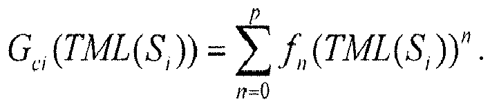
- In the equations, p may be greater than or equal to 1, and q may be greater than or equal to 1.
- In various embodiments, q may be equal to 2 or 3, satisfying the simulation calculation accuracy for the thermal resistance modification model and reducing the simulation calculation complexity.
- In various embodiments, p may be equal to 2 or 3, satisfying the simulation calculation accuracy for the thermal capacity modification model and reducing the simulation calculation complexity.
- The method of acquiring the thermal diffusion coefficient, the ambient temperature coefficient, the power coefficient, the thermal coefficient, fn, and gn in the self-heating effect model may include: testing the total exposed base area of the device under test exposed by the through holes of the device under test, the total exposed base area of the i-th adjacent device exposed by the through holes of the i-th adjacent device, the power of the device under test, the power of the i-th adjacent device, the distances between the adjacent devices, the distances between the device under test and the adjacent devices, the ambient temperature of the device under test and the adjacent devices, the temperature of the device under test, the temperatures of the adjacent devices, the time constant of the device under test, and the time constants of the adjacent devices; acquiring the difference between the temperature of the device under test and the ambient temperature of the device under test and the adjacent devices, according to the ambient temperature of the device under test and the adjacent devices and the temperature of the device under test; acquiring the difference between the temperature of each adjacent device and the ambient temperature of the device under test and the adjacent devices, according to the ambient temperature of the device under test and the adjacent devices, and the temperature of each adjacent device; obtaining the test values of R th0, Rthi, and Rthm by calculation according to formula PRth = ΔT ; obtaining the test values of C th0, Cthi, and Cthm by calculation according to formula Rth * Cth = Tcon , where Tcon is a time constant; setting test conductions, and performing tests under different test conditions to obtain corresponding test data, performing simulation calculation by plugging the obtained test data into the self-heating effect model, to obtain the values of the thermal diffusion coefficient, the ambient temperature coefficient, the power coefficient, the thermal coefficient, fn , and gn .
- In various embodiments, the method of setting the test conditions may include: setting a first type of test conditions, setting a second type of test conditions, setting a third type of test conditions, and setting a fourth type of test conditions.
- The method of setting the first type of test conditions may include: designing such that: the total exposed base area of the device under test exposed by the through holes of the device under test has different values, and other parameters of the device under test remain the same; and when the total exposed base area of the device under test exposed by the through holes of the device under test has different values, the power of the device under test remains the same, the powers of the adjacent devices remain the same, the total exposed base area of the i-th adjacent device exposed by the through holes of the i-th adjacent device remains the same, the distances between the adjacent devices remain the same, and the distances between the device under test and the adjacent devices remain the same.
- The method of setting the second type of test conditions may include: designing such that: the device under test operates at different operating powers, and other conditions of the device under test remain the same; and when the device under test operates at different operating powers, the powers of the adjacent devices remain the same, the total exposed base area of the device under test exposed by the through holes of the device under test remains the same, the total exposed base area of the i-th adjacent device exposed by the through holes of the i-th adjacent device remains the same, the distances between the adjacent devices remain the same, and the distances between the device under test and the adjacent devices remain the same.
- The method of setting the third type of test conditions may include: designing such that: the total exposed base area of the i-th adjacent device exposed by the through holes of the i-th adjacent device has different values, and the other parameters of the i-th adjacent device remain the same; and when the total exposed base area of the i-th adjacent device exposed by the through holes of the i-th adjacent device has different values, the total exposed base area of the m-th adjacent device exposed by the through holes of the m-th adjacent device remains the same, the total exposed base area of the device under test exposed by the through holes of the device under test remains the same, the power of the device under test remains the same, the power of the i-th adjacent device remains the same, the power of the m-th adjacent device remains the same, the distances between the adjacent devices remain the same, the distances between the device under test and the adjacent devices remain the same.
- The method of setting the fourth type of test conditions may include: designing such that: the i-th adjacent device operates at different operating powers, and other conditions of the i-th adjacent device remain the same; and when the i-th adjacent device operates at different operating powers, the total exposed base area of the device under test exposed by the through holes of the device under test remains the same, the total exposed base area of the i-th adjacent device exposed by the through holes of the i-th adjacent device remains the same, the total exposed base area of the m-th adjacent device exposed by the through holes of the m-th adjacent device remains the same, the power of the m-th adjacent device remains the same, the power of the device under test remains the same, the distances between the adjacent devices remain the same, the distances between the device under test and the adjacent devices remain the same.
- Accordingly, various embodiments further provide a test method.
FIG. 8 illustrates a flow chart of an exemplary test method consistent with various disclosed embodiments. As shown inFIG. 8 , the test method may include: at S81, providing devices including a device under test and one or more adjacent devices surrounding the device under test; at S82, providing a self-heating effect apparatus used for processing the self-heating effect model; at S83, acquiring the thermal level of the device under test by inputting the thermal levels of the adjacent devices, the distance levels between the device under test and the adjacent devices, the vertical thermal diffusion level of the device under test, the power level of the device under test, and the ambient temperature level of the device under test and the adjacent devices, into the thermal temperature feedback model; at S84, acquiring a modified thermal resistance of the device under test by inputting the thermal level of the device under test and the reference thermal resistance into the thermal resistance modification model; and, at S85, acquiring a modified thermal capacity of the device under test by inputting the thermal level of the device under test and the reference thermal capacity into the thermal capacity modification model. - In the disclosed test method, the self-heating effect of the device under test may be tested by adopting the self-heating effect model, such that the heat flow network of the device under test may be accurately acquired.
- Various embodiments of the present invention further provide a self-heating effect apparatus used for processing the disclosed self-heating effect model.
FIG. 9 is a schematic diagram of an exemplary self-heating effect apparatus used for processing a self-heating effect model according to various embodiments of the present invention. - As shown in
FIG. 9 , the self-heatingeffect apparatus 9000 includes amemory 9001 and aprocessor 9002. More devices/components may be added. Thememory 9001 is configured to store program instructions for a self-heating effect model. Theprocessor 9002 is coupled to thememory 9001, and is configured to execute the program instructions and process the disclosed self-heating effect model. - In some embodiments, computer-executable program instructions may be stored in the
memory 9001 and executed by theprocessor 9002 for processing the disclosed self-heating effect model. In other embodiments, a non-transitory computer-readable storage medium may further be included to contain computer-executable program instructions, which may be executed by theprocessor 9002 for processing the disclosed self-heating effect model. Detail descriptions related to the self-heating effect model are not repeated here. - In various embodiments, the exemplary self-heating
effect apparatus 9000 may further include a communications interface configured to obtain information and data for theprocessor 9002 to process the disclosed self-heating effect model. - The present invention provides a self-heating effect model and a test method. The self-heating effect model may be used to characterize a heat flow network of devices which include a device under test and one or more adjacent devices surrounding the device under test. The self-heating effect model may include: a reference thermal resistance and a reference thermal capacity; a thermal temperature feedback model for acquiring the thermal level of the device under test by the thermal levels of the adjacent devices, the distance levels between the device under test and the adjacent devices, the vertical thermal diffusion level of the device under test, the power level of the device under test, and the ambient temperature level of the device under test and the adjacent devices; a thermal resistance modification model used to acquire the modified thermal resistance of the device under test according to the thermal level of the device under test and the reference thermal resistance; a thermal capacity modification model used to acquire the modified thermal capacity of the device under test according to the thermal level of the device under test and the reference thermal capacity. The self-heating effect model may accurately characterize the heat flow network of the device under test.
- In comparison with the existing technology, the present invention provides the technical solutions having the following features.
- The disclosed self-heating effect model may include a thermal temperature feedback model, a thermal resistance modification model and a thermal capacity modification model. The thermal temperature feedback model may take into account the influences on the thermal level of the device under test by the distance levels between the device under test and the adjacent devices, the thermal levels of the adjacent devices, the vertical thermal diffusion level of the device under test, the power level of the device under test, and the ambient temperature level of the device under test and the adjacent devices. Accordingly, the thermal temperature feedback model may accurately characterize the device thermal level.
- The thermal resistance modification model may be used to acquire the modified thermal resistance according to the thermal level of the device under test and the reference thermal resistance. The thermal capacity modification model may be used to acquire the modified thermal capacity of the device under test according to the thermal level of the device under test and the reference thermal capacity. Because of the accurate characterization of the device thermal level, the thermal resistance modification model may accurately characterize the modified thermal resistance of the device under test, and the thermal capacity modification model may accurately characterize the modified thermal capacity of the device under test. Thus, the self-heating effect model may accurately characterize the heat flow network of the device under test.
- In the disclosed test method, the self-heating effect of the device under test may be tested by the self-heating effect model, such that the heat flow network of the device under test may be accurately acquired.
Claims (15)
- A self-heating effect apparatus comprising:a memory, storing program instructions for a self-heating effect model, anda processor, coupled to the memory and, when executing the program instructions, configured to process the self-heating effect model for characterizing a heat flow network of devices, the devices including a device under test and one or more adjacent devices surrounding the device under test, wherein the self-heating effect model includes:a thermal temperature feedback model, used to acquire a thermal level of the device under test, by thermal levels of the one or more adjacent devices, distance levels between the device under test and the one or more adjacent devices, a vertical thermal diffusion level of the device under test, a power level of the device under test, and an ambient temperature level of the device under test and the one or more adjacent devices;a thermal resistance modification model, used to acquire a modified thermal resistance of the device under test according to the thermal level of the device under test and a reference thermal resistance; anda thermal capacity modification model, used to acquire a modified thermal capacity of the device under test according to the thermal level of the device under test and a reference thermal capacity.
- The apparatus according to claim 1, wherein:the thermal temperature feedback model comprises: a temperature level model for acquiring a temperature level of a device; and a thermal level model for acquiring a thermal level of the device.
- The apparatus according to claim 2, wherein:temperature levels of the devices include a temperature level of the device under test and temperature levels of the one or more adjacent devices; andthermal levels of the devices include a thermal level of the device under test and thermal levels of the one or more adjacent devices.
- The apparatus according to claim 3, wherein:the thermal level of the device under test is denoted as TML(S 0) and acquired by the thermal level model, according to the temperature level, denoted as WTL(S 0), of the device under test and the power level, denoted as EPD(S 0), of the device under test, TML(S0 ) = (WTL(S 0) + EPD(S 0)) * ETR, wherein ETR is a thermal coefficient; andthe temperature level, denoted as WTL(S 0), of the device under test is acquired by the temperature level model, according to the distance levels between the device under test and the one or more adjacent devices, the thermal levels of the one or more adjacent devices, the vertical thermal diffusion level, denoted as VHD(S 0), of the device under test, and the ambient temperature level, denoted as ETS, of the device under test and the one or more adjacent devices,
 W i0 represents a distance level between the device under test and an i-th adjacent device;TML(Si ) represents the thermal level of the i-th adjacent device; andk equals to a total quantity of the one or more adjacent devices.
 - The apparatus according to claim 4, wherein:the thermal level, denoted as TML(Si ), of the i-th adjacent device is acquired by the thermal level model, according to the temperature level, denoted as WTL(Si ), of the i-th adjacent device and the power level, denoted as EPD(Si ), of the i-th adjacent device, TML(Si ) = (WTL(Si ) + EPD(Si )) * ETR ; andthe temperature level, denoted as WTL(Si ), of the i-th adjacent device is acquired by the temperature level model, according to the distance level, denoted as W i0, between the i-th adjacent device and the device under test, distance levels between the i-th adjacent device and adjacent devices surrounding the i-th adjacent device, the thermal level, denoted as TML(S 0), of the device under test, thermal levels of the adjacent devices surrounding the i-th adjacent device, the vertical thermal diffusion level, denoted as VHD(Si ), of the i-th adjacent device, and the ambient temperature, denoted as ETS, of the device under test and the one or more adjacent devices,
 Wim represents the distance level between the i-th adjacent device and an m-th adjacent device; andTML(Sm ) represents the thermal level of the m-th adjacent device.
 - The apparatus according to claim 5, wherein:the distance level, denoted as Wim, between the i-th adjacent device and the m-th adjacent device is acquired according to a distance, denoted as Lim, between the i-th adjacent device and the m-th adjacent device, Wim =1/Lim ; or, alternatively,the distance level, denoted as Wim, between the i-th adjacent device and the m-th adjacent device is acquired according to a distance, denoted as Lim, between the i-th adjacent device and the m-th adjacent device, Wim =1/Lim 2.
- The apparatus according to claim 5 or 6, wherein:the i-th adjacent device includes a base of the i-th adjacent device, and one or more through holes of the i-th adjacent device are formed above a surface of the base of the i-th adjacent device; andthe vertical thermal diffusion level, denoted as VHD(Si ), of the i-th adjacent device is acquired according to a total exposed area, denoted as Ai , of the base of the i-th adjacent device exposed by the one or more through holes of the i-th adjacent device,

- The apparatus according to anyone of the claims 5-7, wherein:the power level, denoted as EPD(Si ), of the i-th adjacent device is acquired according to a power, denoted as Pi , of the i-th adjacent device, EPD(Si ) = b * Pi.
- The apparatus according to anyone of the claims 5-8, wherein:the thermal resistance modification model is further used to acquire a modified thermal resistance of the i-th adjacent device according to the thermal level of the i-th adjacent device and the reference thermal resistance; andthe thermal capacity modification model is further used to acquire a modified thermal capacity of the i-th adjacent device according to the thermal level of the i-th adjacent device and the reference thermal capacity; andwherein preferably:the modified thermal resistance, denoted as Rthi, of the i-th adjacent device is acquired by the thermal resistance modification model according to the thermal level, denoted as TML(Si ), of the i-th adjacent device, and the reference thermal resistance, denoted as Rth_base, Rthi = GRi (TML(Si )) * Rth_base , and
 the modified thermal capacity, denoted as Cthi, of the i-th adjacent device is acquired by the thermal capacity modification model according to the thermal level, denoted as TML(Si ), of the i-th adjacent device and the reference thermal capacity Cth_base, Cthi = Gci(TML(Si )) * Cth_base, and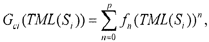
- The apparatus according to anyone of the claims 1-9, wherein:the modified thermal resistance, denoted as R th0, of the device under test is acquired by the thermal resistance modification model according to the thermal level, denoted as TML(S 0), of the device under test and the reference thermal resistance, denoted as Rth_base , Rtho = GRo (TML(S 0)) * Rth_base, and
 the modified thermal capacity, denoted as C th0, of the device under test is acquired by the thermal capacity modification model according to the thermal level, denoted as TML(S 0), of the device under test and the reference thermal capacity Cth_base, Cth0 = Gco (TML(S 0)) * Cth_base, and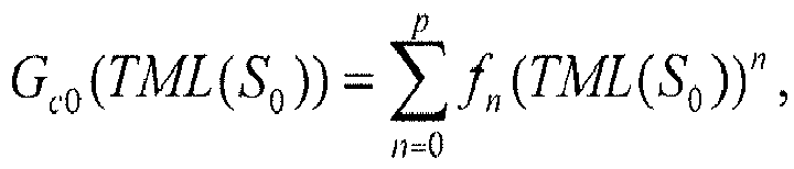
- The apparatus according to claim 9 or 10, wherein:q is equal to 2 or 3; andp is equal to 2 or 3.
- The apparatus according to anyone of the claims 1-11, wherein:a distance level, denoted as W i0 , between the device under test and an i-th adjacent device is acquired according to a distance, denoted as L i0, between the device under test and the i-th adjacent device, W i0=1/L i0 ; or, alternatively,a distance level, denoted as W i0 , between the device under test and an i-th adjacent device is acquired according to a distance, denoted as L i0, between the device under test and the i-th adjacent device, W i0=1/L i0 2.
- The apparatus according to anyone of the claims 1-12, wherein:the device under test includes a base of the device under test, and one or more through holes of the device under test are formed above a surface of the base of the device under test; andthe vertical thermal diffusion level, denoted as VHD(S 0), of the device under test is acquired according to a total exposed area, denoted as A 0, of the base of the device under test exposed by the one or more through holes of the device under test,

- The apparatus according to anyone of the claims 1-13, wherein:the power level, denoted as EPD(S 0), of the device under test is acquired according to a power, denoted as P 0, of the device under test, EPD(S 0) = b * P 0; and/orthe ambient temperature level, denoted as ETS, of the device under test and the one or more adjacent devices is acquired according to an ambient temperature, denoted as Ts , of the device under test and the one or more adjacent devices, ETS = tTs.
- A test method, comprising:providing devices including a device under test and one or more adjacent devices surrounding the device under test;providing a self-heating effect apparatus including:a memory, storing program instructions for a self-heating effect model, anda processor, coupled to the memory and, when executing the program instructions, configured to process the self-heating effect model for characterizing a heat flow network of devices, the devices including a device under test and one or more adjacent devices surrounding the device under test, wherein the self-heating effect model includes:a thermal temperature feedback model, used to acquire a thermal level of the device under test, by thermal levels of the one or more adjacent devices, distance levels between the device under test and the one or more adjacent devices, a vertical thermal diffusion level of the device under test, a power level of the device under test, and an ambient temperature level of the device under test and the one or more adjacent devices,a thermal resistance modification model, used to acquire a modified thermal resistance of the device under test according to the thermal level of the device under test and a reference thermal resistance, anda thermal capacity modification model, used to acquire a modified thermal capacity of the device under test according to the thermal level of the device under test and a reference thermal capacity;acquiring a thermal level of the device under test, by inputting the thermal levels of the one or more adjacent devices, the distance levels between the device under test and the one or more adjacent devices, the vertical thermal diffusion level of the device under test, the power level of the device under test, and the ambient temperature level of the device under test and the one or more adjacent devices, into the thermal temperature feedback model;acquiring the modified thermal resistance of the device under test by inputting the thermal level of the device under test and the reference thermal resistance into the thermal resistance modification model; andacquiring the modified thermal capacity of the device under test by inputting the thermal level of the device under test and the reference thermal capacity into the thermal capacity modification model.
Applications Claiming Priority (1)
| Application Number | Priority Date | Filing Date | Title |
|---|---|---|---|
| CN201611207623.1A CN108242200B (en) | 2016-12-23 | 2016-12-23 | Self-heating effect model and test method |
Publications (1)
| Publication Number | Publication Date |
|---|---|
| EP3340087A1 true EP3340087A1 (en) | 2018-06-27 |
Family
ID=60781587
Family Applications (1)
| Application Number | Title | Priority Date | Filing Date |
|---|---|---|---|
| EP17207628.3A Withdrawn EP3340087A1 (en) | 2016-12-23 | 2017-12-15 | Self-heating effect apparatus and test method |
Country Status (3)
| Country | Link |
|---|---|
| US (1) | US11137440B2 (en) |
| EP (1) | EP3340087A1 (en) |
| CN (1) | CN108242200B (en) |
Families Citing this family (1)
| Publication number | Priority date | Publication date | Assignee | Title |
|---|---|---|---|---|
| CN112464597B (en) * | 2020-12-03 | 2024-04-12 | 成都海光微电子技术有限公司 | Circuit simulation method and device, storage medium and electronic equipment |
Citations (3)
| Publication number | Priority date | Publication date | Assignee | Title |
|---|---|---|---|---|
| US20150370937A1 (en) * | 2014-06-18 | 2015-12-24 | Taiwan Semiconductor Manufacturing Company, Ltd. | Integrated circuit temperature distribution determination |
| US20160048622A1 (en) * | 2014-08-18 | 2016-02-18 | Jongwook JEON | Simulation system estimating self-heating characteristic of circuit and design method thereof |
| US20160357898A1 (en) * | 2015-06-02 | 2016-12-08 | Global Foundries Inc. | Design of temperature-compliant integrated circuits |
Family Cites Families (6)
| Publication number | Priority date | Publication date | Assignee | Title |
|---|---|---|---|---|
| JP4081915B2 (en) * | 1998-05-14 | 2008-04-30 | 株式会社デンソー | Logic simulation method and apparatus |
| US9740804B2 (en) * | 2014-11-03 | 2017-08-22 | Mentor Graphics Corporation | Chip-scale electrothermal analysis |
| CN104331580B (en) * | 2014-11-20 | 2017-07-11 | 上海华虹宏力半导体制造有限公司 | The method that self-heating effect is described using high voltage field effect transistor sub-circuit model |
| TWI522830B (en) * | 2015-01-09 | 2016-02-21 | 國立成功大學 | Thermal simulation device and method for integrated circuits |
| CN106158830B (en) * | 2016-07-29 | 2019-01-18 | 上海华力微电子有限公司 | Self-heating electro-migration testing structure and wafer scale self-heating electro-migration testing method |
| CN106093744B (en) * | 2016-08-04 | 2019-03-05 | 中国科学院微电子研究所 | A method of obtaining thermal resistance |
-
2016
- 2016-12-23 CN CN201611207623.1A patent/CN108242200B/en active Active
-
2017
- 2017-12-15 EP EP17207628.3A patent/EP3340087A1/en not_active Withdrawn
- 2017-12-22 US US15/853,131 patent/US11137440B2/en active Active
Patent Citations (3)
| Publication number | Priority date | Publication date | Assignee | Title |
|---|---|---|---|---|
| US20150370937A1 (en) * | 2014-06-18 | 2015-12-24 | Taiwan Semiconductor Manufacturing Company, Ltd. | Integrated circuit temperature distribution determination |
| US20160048622A1 (en) * | 2014-08-18 | 2016-02-18 | Jongwook JEON | Simulation system estimating self-heating characteristic of circuit and design method thereof |
| US20160357898A1 (en) * | 2015-06-02 | 2016-12-08 | Global Foundries Inc. | Design of temperature-compliant integrated circuits |
Also Published As
| Publication number | Publication date |
|---|---|
| US11137440B2 (en) | 2021-10-05 |
| CN108242200A (en) | 2018-07-03 |
| CN108242200B (en) | 2020-06-09 |
| US20180180664A1 (en) | 2018-06-28 |
Similar Documents
| Publication | Publication Date | Title |
|---|---|---|
| US7302378B2 (en) | Electrostatic discharge protection device modeling method and electrostatic discharge simulation method | |
| US10289777B2 (en) | Integrated circuit designs based on temperature distribution determination | |
| US7240308B2 (en) | Simulation method for semiconductor circuit device and simulator for semiconductor circuit device | |
| US6541285B2 (en) | Method of estimating lifetime of semiconductor device, and method of reliability simulation | |
| Nicosia et al. | Characterization and modeling of temperature effects in 3-D NAND Flash arrays—Part II: Random telegraph noise | |
| US20120297351A1 (en) | Methods of modeling a transistor and apparatus used therein | |
| WO2012051899A1 (en) | Method for determining bsimsoi4 direct current model parameter | |
| CN114417581B (en) | Simulation methods and systems based on SPICE models | |
| CN105095537A (en) | Simulation model of high voltage device and modeling method for simulation model of high voltage device | |
| US11137440B2 (en) | Self-heating effect apparatus and test method | |
| US9268743B2 (en) | Method for determining a mathematical model of the electric behavior of a PN junction diode, and corresponding device | |
| JP2005259778A (en) | Reliability simulation method for semiconductor device | |
| US9996650B2 (en) | Modeling the performance of a field effect transistor having a dynamically depleted channel region | |
| CN118965818B (en) | Semiconductor device life prediction method, device, electronic equipment and medium | |
| US20080027700A1 (en) | Simulation model of BT instability of transistor | |
| Kumar et al. | Lateral profiling of trapped charge in SONOS Flash EEPROMs programmed using CHE injection | |
| JP4390594B2 (en) | Semiconductor device evaluation method | |
| US20160321391A1 (en) | Determining correlation coefficient(s) among different field effect transistor types and/or among different electrical parameter types | |
| Bergamaschi et al. | Experimental analysis of self-heating effects using the pulsed IV method in junctionless nanowire transistors | |
| US9209167B2 (en) | Determining threshold voltage variations in field effect transistors | |
| Sozzi et al. | A review of the use of electro-thermal simulations for the analysis of heterostructure FETs | |
| KR100403624B1 (en) | A proved extraction method for model parameter of SPICE | |
| Tondelli | Modellazione e Caratterizzazione Termica in Regime Statico e DInamico in FDSOI MOSFET e FinFET nanoscopici | |
| Hong | Modeling of Ids-Vds Characteristics of Short-Channel Double-Gate (DG) MOSFETs | |
| JP2003110106A (en) | Partially depleted SOI transistor SPICE parameter extraction method |
Legal Events
| Date | Code | Title | Description |
|---|---|---|---|
| PUAI | Public reference made under article 153(3) epc to a published international application that has entered the european phase |
Free format text: ORIGINAL CODE: 0009012 |
|
| STAA | Information on the status of an ep patent application or granted ep patent |
Free format text: STATUS: THE APPLICATION HAS BEEN PUBLISHED |
|
| AK | Designated contracting states |
Kind code of ref document: A1 Designated state(s): AL AT BE BG CH CY CZ DE DK EE ES FI FR GB GR HR HU IE IS IT LI LT LU LV MC MK MT NL NO PL PT RO RS SE SI SK SM TR |
|
| AX | Request for extension of the european patent |
Extension state: BA ME |
|
| RAP1 | Party data changed (applicant data changed or rights of an application transferred) |
Owner name: SEMICONDUCTOR MANUFACTURING INTERNATIONAL (SHANGHA Owner name: SEMICONDUCTOR MANUFACTURING INTERNATIONAL (BEIJING |
|
| STAA | Information on the status of an ep patent application or granted ep patent |
Free format text: STATUS: REQUEST FOR EXAMINATION WAS MADE |
|
| 17P | Request for examination filed |
Effective date: 20181220 |
|
| RBV | Designated contracting states (corrected) |
Designated state(s): AL AT BE BG CH CY CZ DE DK EE ES FI FR GB GR HR HU IE IS IT LI LT LU LV MC MK MT NL NO PL PT RO RS SE SI SK SM TR |
|
| STAA | Information on the status of an ep patent application or granted ep patent |
Free format text: STATUS: EXAMINATION IS IN PROGRESS |
|
| 17Q | First examination report despatched |
Effective date: 20210506 |
|
| STAA | Information on the status of an ep patent application or granted ep patent |
Free format text: STATUS: THE APPLICATION IS DEEMED TO BE WITHDRAWN |
|
| 18D | Application deemed to be withdrawn |
Effective date: 20210917 |