EP3338366B1 - Amplificateur de signal de dispositif sans fil - Google Patents
Amplificateur de signal de dispositif sans fil Download PDFInfo
- Publication number
- EP3338366B1 EP3338366B1 EP16837836.2A EP16837836A EP3338366B1 EP 3338366 B1 EP3338366 B1 EP 3338366B1 EP 16837836 A EP16837836 A EP 16837836A EP 3338366 B1 EP3338366 B1 EP 3338366B1
- Authority
- EP
- European Patent Office
- Prior art keywords
- signal
- antenna
- signals
- booster
- path
- Prior art date
- Legal status (The legal status is an assumption and is not a legal conclusion. Google has not performed a legal analysis and makes no representation as to the accuracy of the status listed.)
- Active
Links
- 230000003321 amplification Effects 0.000 claims description 58
- 238000003199 nucleic acid amplification method Methods 0.000 claims description 58
- 238000004891 communication Methods 0.000 claims description 44
- 238000001914 filtration Methods 0.000 claims description 31
- 230000001413 cellular effect Effects 0.000 description 67
- 230000008878 coupling Effects 0.000 description 27
- 238000010168 coupling process Methods 0.000 description 27
- 238000005859 coupling reaction Methods 0.000 description 27
- 238000000034 method Methods 0.000 description 12
- 230000005540 biological transmission Effects 0.000 description 6
- 238000012545 processing Methods 0.000 description 6
- 238000005516 engineering process Methods 0.000 description 5
- 230000010267 cellular communication Effects 0.000 description 4
- 230000005055 memory storage Effects 0.000 description 4
- 230000035945 sensitivity Effects 0.000 description 4
- 230000006870 function Effects 0.000 description 3
- 239000000463 material Substances 0.000 description 3
- 230000005855 radiation Effects 0.000 description 3
- 230000002745 absorbent Effects 0.000 description 2
- 239000002250 absorbent Substances 0.000 description 2
- 238000010521 absorption reaction Methods 0.000 description 2
- 238000013459 approach Methods 0.000 description 2
- 238000003491 array Methods 0.000 description 2
- 230000008901 benefit Effects 0.000 description 2
- 230000006872 improvement Effects 0.000 description 2
- 229910052751 metal Inorganic materials 0.000 description 2
- 239000002184 metal Substances 0.000 description 2
- 230000008569 process Effects 0.000 description 2
- 229910052782 aluminium Inorganic materials 0.000 description 1
- XAGFODPZIPBFFR-UHFFFAOYSA-N aluminium Chemical compound [Al] XAGFODPZIPBFFR-UHFFFAOYSA-N 0.000 description 1
- 239000003795 chemical substances by application Substances 0.000 description 1
- 230000001010 compromised effect Effects 0.000 description 1
- 230000001934 delay Effects 0.000 description 1
- 230000001419 dependent effect Effects 0.000 description 1
- 238000005562 fading Methods 0.000 description 1
- 230000010354 integration Effects 0.000 description 1
- 238000002955 isolation Methods 0.000 description 1
- 239000004973 liquid crystal related substance Substances 0.000 description 1
- 230000007774 longterm Effects 0.000 description 1
- 230000007257 malfunction Effects 0.000 description 1
- 238000010295 mobile communication Methods 0.000 description 1
- 238000012986 modification Methods 0.000 description 1
- 230000004048 modification Effects 0.000 description 1
- 230000003287 optical effect Effects 0.000 description 1
- 230000010355 oscillation Effects 0.000 description 1
- 239000004065 semiconductor Substances 0.000 description 1
- 230000035939 shock Effects 0.000 description 1
- 230000011664 signaling Effects 0.000 description 1
- 239000007787 solid Substances 0.000 description 1
Images


Classifications
-
- H—ELECTRICITY
- H04—ELECTRIC COMMUNICATION TECHNIQUE
- H04W—WIRELESS COMMUNICATION NETWORKS
- H04W52/00—Power management, e.g. TPC [Transmission Power Control], power saving or power classes
- H04W52/02—Power saving arrangements
- H04W52/0209—Power saving arrangements in terminal devices
- H04W52/0225—Power saving arrangements in terminal devices using monitoring of external events, e.g. the presence of a signal
- H04W52/0229—Power saving arrangements in terminal devices using monitoring of external events, e.g. the presence of a signal where the received signal is a wanted signal
-
- H—ELECTRICITY
- H04—ELECTRIC COMMUNICATION TECHNIQUE
- H04B—TRANSMISSION
- H04B7/00—Radio transmission systems, i.e. using radiation field
- H04B7/02—Diversity systems; Multi-antenna system, i.e. transmission or reception using multiple antennas
- H04B7/04—Diversity systems; Multi-antenna system, i.e. transmission or reception using multiple antennas using two or more spaced independent antennas
-
- H—ELECTRICITY
- H04—ELECTRIC COMMUNICATION TECHNIQUE
- H04B—TRANSMISSION
- H04B7/00—Radio transmission systems, i.e. using radiation field
- H04B7/14—Relay systems
- H04B7/15—Active relay systems
- H04B7/155—Ground-based stations
-
- H—ELECTRICITY
- H04—ELECTRIC COMMUNICATION TECHNIQUE
- H04B—TRANSMISSION
- H04B7/00—Radio transmission systems, i.e. using radiation field
- H04B7/14—Relay systems
- H04B7/15—Active relay systems
- H04B7/155—Ground-based stations
- H04B7/15557—Selecting relay station operation mode, e.g. between amplify and forward mode, decode and forward mode or FDD - and TDD mode
-
- H—ELECTRICITY
- H04—ELECTRIC COMMUNICATION TECHNIQUE
- H04L—TRANSMISSION OF DIGITAL INFORMATION, e.g. TELEGRAPHIC COMMUNICATION
- H04L43/00—Arrangements for monitoring or testing data switching networks
- H04L43/02—Capturing of monitoring data
- H04L43/028—Capturing of monitoring data by filtering
-
- H—ELECTRICITY
- H04—ELECTRIC COMMUNICATION TECHNIQUE
- H04L—TRANSMISSION OF DIGITAL INFORMATION, e.g. TELEGRAPHIC COMMUNICATION
- H04L43/00—Arrangements for monitoring or testing data switching networks
- H04L43/16—Threshold monitoring
-
- H—ELECTRICITY
- H04—ELECTRIC COMMUNICATION TECHNIQUE
- H04W—WIRELESS COMMUNICATION NETWORKS
- H04W40/00—Communication routing or communication path finding
- H04W40/02—Communication route or path selection, e.g. power-based or shortest path routing
- H04W40/22—Communication route or path selection, e.g. power-based or shortest path routing using selective relaying for reaching a BTS [Base Transceiver Station] or an access point
-
- H—ELECTRICITY
- H04—ELECTRIC COMMUNICATION TECHNIQUE
- H04W—WIRELESS COMMUNICATION NETWORKS
- H04W52/00—Power management, e.g. TPC [Transmission Power Control], power saving or power classes
- H04W52/04—TPC
- H04W52/52—TPC using AGC [Automatic Gain Control] circuits or amplifiers
-
- H—ELECTRICITY
- H04—ELECTRIC COMMUNICATION TECHNIQUE
- H04W—WIRELESS COMMUNICATION NETWORKS
- H04W88/00—Devices specially adapted for wireless communication networks, e.g. terminals, base stations or access point devices
- H04W88/02—Terminal devices
- H04W88/04—Terminal devices adapted for relaying to or from another terminal or user
-
- H—ELECTRICITY
- H04—ELECTRIC COMMUNICATION TECHNIQUE
- H04W—WIRELESS COMMUNICATION NETWORKS
- H04W88/00—Devices specially adapted for wireless communication networks, e.g. terminals, base stations or access point devices
- H04W88/08—Access point devices
-
- Y—GENERAL TAGGING OF NEW TECHNOLOGICAL DEVELOPMENTS; GENERAL TAGGING OF CROSS-SECTIONAL TECHNOLOGIES SPANNING OVER SEVERAL SECTIONS OF THE IPC; TECHNICAL SUBJECTS COVERED BY FORMER USPC CROSS-REFERENCE ART COLLECTIONS [XRACs] AND DIGESTS
- Y02—TECHNOLOGIES OR APPLICATIONS FOR MITIGATION OR ADAPTATION AGAINST CLIMATE CHANGE
- Y02D—CLIMATE CHANGE MITIGATION TECHNOLOGIES IN INFORMATION AND COMMUNICATION TECHNOLOGIES [ICT], I.E. INFORMATION AND COMMUNICATION TECHNOLOGIES AIMING AT THE REDUCTION OF THEIR OWN ENERGY USE
- Y02D30/00—Reducing energy consumption in communication networks
- Y02D30/70—Reducing energy consumption in communication networks in wireless communication networks
Definitions
- Signal boosters can be used to increase the quality of wireless communication between a wireless device and a wireless communication access point, such as a cell tower. Signal boosters can improve the quality of the wireless communication by amplifying, filtering, and/or applying other processing techniques to uplink and downlink signals communicated between the wireless device and the wireless communication access point.
- the signal booster can receive, via an antenna, downlink signals from the wireless communication access point.
- the signal booster can amplify the downlink signal and then provide an amplified downlink signal to the wireless device.
- the signal booster can act as a relay between the wireless device and the wireless communication access point.
- the wireless device can receive a stronger signal from the wireless communication access point.
- uplink signals from the wireless device e.g., telephone calls and other data
- the signal booster can amplify the uplink signals before communicating, via the antenna, the uplink signals to the wireless communication access point.
- US9048940B2 teaches a bypass circuit between an NC port of a first relay and an NC port of a second relay, an RF amplifier circuit between an NO port of the first relay and an NO port of the second relay. Either the NO ports are open or the NC ports are open.
- US2013/149957A1 teaches a pair of switches that direct a signal to a repeater circuit, or cause the signal to bypass the repeater circuit by directing the signal to a transmission line connecting the pair of switches.
- FIG. 1 illustrates an exemplary signal booster 120 in communication with a wireless device 110 and a base station 130.
- the signal booster 120 can be referred to as a repeater or signal amplifier.
- a repeater can be an electronic device used to amplify (or boost) signals.
- the signal booster 120 (also referred to as a cellular signal amplifier) can improve the quality of wireless communication by amplifying, filtering, and/or applying other processing techniques via a signal amplifier 122 to uplink signals communicated from the wireless device 110 to the base station 130 and/or downlink signals communicated from the base station 130 to the wireless device 110.
- the signal booster 120 can amplify or boost uplink signals and/or downlink signals bidirectionally.
- the signal booster 120 can be at a fixed location, such as in a home or office.
- the signal booster 120 can be attached to a mobile object, such as a vehicle or a wireless device 110.
- the signal booster 120 can include an integrated device antenna 124 (e.g., an inside antenna or a coupling antenna) and an integrated node antenna 126 (e.g., an outside antenna).
- the integrated node antenna 126 can receive the downlink signal from the base station 130.
- the downlink signal can be provided to the signal amplifier 122 via a second coaxial cable 127 or other type of radio frequency connection operable to communicate radio frequency signals.
- the signal amplifier 122 can include one or more cellular signal amplifiers for amplification and filtering.
- the downlink signal that has been amplified and filtered can be provided to the integrated device antenna 124 via a first coaxial cable 125 or other type of radio frequency connection operable to communicate radio frequency signals.
- the integrated device antenna 124 can wirelessly communicate the downlink signal that has been amplified and filtered to the wireless device 110.
- the integrated device antenna 124 can receive an uplink signal from the wireless device 110.
- the uplink signal can be provided to the signal amplifier 122 via the first coaxial cable 125 or other type of radio frequency connection operable to communicate radio frequency signals.
- the signal amplifier 122 can include one or more cellular signal amplifiers for amplification and filtering.
- the uplink signal that has been amplified and filtered can be provided to the integrated node antenna 126 via the second coaxial cable 127 or other type of radio frequency connection operable to communicate radio frequency signals.
- the integrated device antenna 126 can communicate the uplink signal that has been amplified and filtered to the base station 130.
- the signal booster 120 can send uplink signals to a node and/or receive downlink signals from the node.
- the node can comprise a wireless wide area network (WWAN) access point (AP), a base station (BS), an evolved Node B (eNB), a baseband unit (BBU), a remote radio head (RRH), a remote radio equipment (RRE), a relay station (RS), a radio equipment (RE), a remote radio unit (RRU), a central processing module (CPM), or another type of WWAN access point.
- WWAN wireless wide area network
- AP wireless wide area network
- BS base station
- eNB evolved Node B
- BBU baseband unit
- RRH remote radio head
- RRE remote radio equipment
- RS relay station
- RE radio equipment
- RRU remote radio unit
- CCM central processing module
- the signal booster 120 can amplify uplink signals, and then send amplified uplink signals to the node.
- the uplink signals can be passed without amplification or filtering.
- the uplink signals can be communicated from the wireless device 110 to the node (e.g., eNodeB) while bypassing the signal booster 120.
- the signal booster 120 used to amplify the uplink and/or a downlink signal is a handheld booster.
- the handheld booster can be implemented in a sleeve (or case) of the wireless device 110.
- the wireless device sleeve may be attached to the wireless device 110, but may be removed as needed.
- the signal booster 120 can automatically power down or cease amplification when the wireless device 110 approaches a particular base station.
- the signal booster 120 may determine to stop performing signal amplification when the quality of uplink and/or downlink signals is above a defined threshold based on a location of the wireless device 110 in relation to the base station 130.
- the signal booster 120 can include a battery to provide power to various components, such as the signal amplifier 122, the integrated device antenna 124 and the integrated node antenna 126.
- the battery can also power the wireless device 110 (e.g., phone or tablet).
- the signal booster 120 can receive power from the wireless device 110.
- the signal booster 120 can be a Federal Communications Commission (FCC)-compatible consumer signal booster.
- the signal booster 120 can be compatible with FCC Part 20 or 47 Code of Federal Regulations (C.F.R.) Part 20.21 (March 21, 2013 ).
- the handheld booster can operate on the frequencies used for the provision of subscriber-based services under parts 22 (Cellular), 24 (Broadband PCS), 27 (AWS-1, 700 MHz Lower A-E Blocks, and 700 MHz Upper C Block), and 90 (Specialized Mobile Radio) of 47 C.F.R.
- the signal booster 120 can be configured to automatically self-monitor its operation to ensure compliance with applicable noise and gain limits.
- the signal booster 120 can either self-correct or shut down automatically if the signal booster's operations violate the regulations defined in FCC Part 20.21.
- the signal booster 120 can improve the wireless connection between the wireless device 110 and the base station 130 (e.g., cell tower) or another type of wireless wide area network (WWAN) access point (AP).
- the signal booster 120 can boost signals for cellular standards, such as the Third Generation Partnership Project (3GPP) Long Term Evolution (LTE) Release 8, 9, 10, 11, 12 or 13 standards or Institute of Electronics and Electrical Engineers (IEEE) 802.16.
- 3GPP Third Generation Partnership Project
- LTE Long Term Evolution
- IEEE Institute of Electronics and Electrical Engineers
- the signal booster 120 can boost signals for 3GPP LTE Release 12.0.0 (July 2013 ) or other desired releases.
- the signal booster 120 can boost signals from the 3GPP Technical Specification 36.101 (Release 12 Jun 2015 ) bands or LTE frequency bands.
- the signal booster 120 can boost signals from the LTE frequency bands: 2, 4, 5, 12, 13, 17, and 25.
- the signal booster 120 can boost selected frequency bands based on the country or region in which the signal booster is used.
- the signal booster 120 can boost time division duplexing (TDD) and/or frequency division duplexing (FDD) signals.
- TDD time division duplexing
- FDD frequency division duplexing
- the number of LTE frequency bands and the level of signal improvement can vary based on a particular wireless device, cellular node, or location. Additional domestic and international frequencies can also be included to offer increased functionality. Selected models of the signal booster 120 can be configured to operate with selected frequency bands based on the location of use. In another example, the signal booster 120 can automatically sense from the wireless device 110 or base station 130 (or GPS, etc.) which frequencies are used, which can be a benefit for international travelers.
- the integrated device antenna 124 and the integrated node antenna 126 can be comprised of a single antenna, an antenna array, or have a telescoping form-factor.
- the integrated device antenna 124 and the integrated node antenna 126 can be a microchip antenna.
- An example of a microchip antenna is AMMAL001.
- the integrated device antenna 124 and the integrated node antenna 126 can be a printed circuit board (PCB) antenna.
- PCB printed circuit board
- An example of a PCB antenna is TE 2118310-1.
- the integrated device antenna 124 can receive uplink (UL) signals from the wireless device 100 and transmit DL signals to the wireless device 100 using a single antenna.
- the integrated device antenna 124 can receive UL signals from the wireless device 100 using a dedicated UL antenna, and the integrated device antenna 124 can transmit DL signals to the wireless device 100 using a dedicated DL antenna.
- the integrated device antenna 124 can wireless communicate with one or more antennas in the wireless device 110. In another example, the integrated device antenna 124 can be coupled to one or more antennas in the wireless device 110. In addition, the integrated device antenna 124 can communicate with the wireless device 110 using near field communication, or alternatively, the integrated device antenna 124 can communicate with the wireless device 110 using far field communication.
- the integrated node antenna 126 can receive downlink (DL) signals from the base station 130 and transmit uplink (UL) signals to the base station 130 via a single antenna.
- the integrated node antenna 126 can receive DL signals from the base station 130 using a dedicated DL antenna, and the integrated node antenna 126 can transmit UL signals to the base station 130 using a dedicated UL antenna.
- multiple signal boosters can be used to amplify UL and DL signals.
- a first signal booster can be used to amplify UL signals and a second signal booster can be used to amplify DL signals.
- different signal boosters can be used to amplify different frequency ranges.
- a phone-specific case of the handheld booster can be configured for a specific type or model of wireless device.
- the phone-specific case can be configured with the integrated device antenna 124 located at a desired location to enable communication with an antenna of the specific wireless device.
- amplification and filtering of the uplink and downlink signals can be provided to optimize the operation of the specific wireless device.
- the handheld booster can be configured to communicate with a wide range of wireless devices.
- the handheld booster can be adjustable to be configured for multiple wireless devices.
- the handheld booster 120 when the signal booster 120 is a handheld booster, the handheld booster can be configured to identify when the wireless device 110 receives a relatively strong downlink signal.
- a strong downlink signal can be a downlink signal with a signal strength greater than approximately -80dBm.
- the handheld booster can be configured to automatically turn off selected features, such as amplification, to conserve battery life.
- the integrated booster can be configured to provide amplification of the downlink signal.
- An example of a weak downlink signal can be a downlink signal with a signal strength less than -80dBm.
- the handheld booster can be designed, certified and produced in view of a specific absorption rate (SAR).
- SAR absorption rate
- Many countries have SAR limits which can limit the amount of RF radiation that can be transmitted by a wireless device. This can protect users from harmful amounts of radiation being absorbed in their hand, body, or head.
- a telescoping integrated node antenna may help to remove the radiation from the immediate area of the user.
- the handheld booster can be certified to be used away from a user, such as in use with Bluetooth headsets, wired headsets, and speaker-phones to allow the SAR rates to be higher than if the handheld booster were used in a location adjacent a user's head. Additionally, Wi-Fi communications can be disabled to reduce SAR values when the SAR limit is exceeded.
- mobile devices are often already at a SAR limit, and the handheld booster can potentially increase the SAR. Therefore, in order to reduce the SAR, the mobile device antenna can be blocked from increasing the SAR.
- a portion of the mobile device can be wrapped in a defined type of metal (e.g., aluminum) or radio frequency (RF) absorbent can be placed between the mobile device and the metal.
- RF radio frequency
- the handheld booster can provide an improved integrated node antenna (for communication with a base station).
- the integrated node antenna can be in a computer chip, printed circuit board (PCB), array, beam-forming array or a telescoping form-factor.
- the handheld booster can also include one or more of: a waterproof casing, a shock absorbent casing, a flip-cover, a wallet, or extra memory storage for the wireless device.
- extra memory storage can be achieved with a direct connection between the handheld booster and the wireless device 110.
- NFC Near-Field Communications
- Bluetooth v4.0 Bluetooth Low Energy
- Bluetooth v4.1 Bluetooth v4.2
- 3GPP LTE Institute of Electronics and Electrical Engineers (IEEE) 802.11a, IEEE 802.11b, IEEE 802.11g, IEEE 802.11n, IEEE 802.11ac, or IEEE 802.11ad
- IEEE 802.11a 802.11a
- IEEE 802.11b 802.11g
- IEEE 802.11n IEEE 802.11n
- IEEE 802.11ac IEEE 802.11ad
- a connector can be used to connect the wireless device 110 to the extra memory storage.
- the handheld booster can include photovoltaic cells or solar panels as a technique of charging the integrated battery and/or a battery of the wireless device 110.
- the handheld booster can be configured to communicate directly with other wireless devices with handheld boosters.
- the integrated node antenna 126 can communicate over Very High Frequency (VHF) communications directly with integrated node antennas of other handheld boosters.
- VHF Very High Frequency
- the handheld booster can be configured to communicate with the wireless device 110 through a direct connection, Near-Field Communications (NFC), Bluetooth v4.0, Bluetooth Low Energy, Bluetooth v4.1, Bluetooth v4.2, Ultra High Frequency (UHF), 3GPP LTE, Institute of Electronics and Electrical Engineers (IEEE) 802.11a, IEEE 802.11b, IEEE 802.11g, IEEE 802.11n, IEEE 802.11ac, IEEE 802.11ad, a TV White Space Band (TVWS), or any other industrial, scientific and medical (ISM) radio band. Examples of such ISM bands include 2.4 GHz, 3.6 GHz, 4.9 GHz, 5 GHz, or 5.9 GHz. This configuration can allow data to pass at high rates between multiple wireless devices with handheld boosters.
- NFC Near-Field Communications
- Bluetooth v4.0 Bluetooth Low Energy
- Bluetooth v4.2 Bluetooth Low Energy
- UHF Ultra High Frequency
- 3GPP LTE Institute of Electronics and Electrical Engineers (IEEE) 802.11a, IEEE 802.11b, IEEE
- This configuration can also allow users to send text messages, initiate phone calls, and engage in video communications between wireless devices with handheld boosters.
- the integrated node antenna 126 can be configured to couple to the wireless device 110. In other words, communications between the integrated node antenna 126 and the wireless device 110 can bypass the integrated booster.
- a separate VHF node antenna can be configured to communicate over VHF communications directly with separate VHF node antennas of other handheld boosters. This configuration can allow the integrated node antenna 126 to be used for simultaneous cellular communications.
- the separate VHF node antenna can be configured to communicate with the wireless device 110 through a direct connection, Near-Field Communications (NFC), Bluetooth v4.0, Bluetooth Low Energy, Bluetooth v4.1, Bluetooth v4.2, Ultra High Frequency (UHF), 3GPP LTE, Institute of Electronics and Electrical Engineers (IEEE) 802.11a, IEEE 802.11b, IEEE 802.11g, IEEE 802.11n, IEEE 802.11ac, IEEE 802.11ad, a TV White Space Band (TVWS), or any other industrial, scientific and medical (ISM) radio band.
- the handheld booster can be configured to determine the SAR value.
- the handheld booster can be configured to disable cellular communications or Wi-Fi communications when a SAR limit is exceeded.
- the signal booster 120 can be configured for satellite communication.
- the integrated node antenna 126 can be configured to act as a satellite communication antenna.
- a separate node antenna can be used for satellite communications.
- the signal booster 120 can extend the range of coverage of the wireless device 110 configured for satellite communication.
- the integrated node antenna 126 can receive downlink signals from satellite communications for the wireless device 110.
- the signal booster 120 can filter and amplify the downlink signals from the satellite communication.
- the wireless device 110 can be configured to couple to the signal booster 120 via a direct connection or an ISM radio band. Examples of such ISM bands include 2.4 GHz, 3.6 GHz, 4.9 GHz, 5 GHz, or 5.9 GHz.
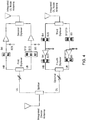
- FIG. 2 illustrates an exemplary bi-directional wireless signal booster 200 configured to amplify uplink (UL) and downlink (DL) signals using a separate signal path for each UL frequency band and DL frequency band and a controller 240.
- An outside antenna 210 or an integrated node antenna, can receive a downlink signal.
- the downlink signal can be received from a base station (not shown).
- the downlink signal can be provided to a first B1/B2 diplexer 212, wherein B1 represents a first frequency band and B2 represents a second frequency band.
- the first B1/B2 diplexer 212 can create a B1 downlink signal path and a B2 downlink signal path.
- a downlink signal that is associated with B1 can travel along the B1 downlink signal path to a first B1 duplexer 214, or a downlink signal that is associated with B2 can travel along the B2 downlink signal path to a first B2 duplexer 216.
- the downlink signal can travel through a series of amplifiers (e.g., A10, A11 and A12) and downlink band pass filters (BPF) to a second B1 duplexer 218.
- amplifiers e.g., A10, A11 and A12
- BPF downlink band pass filters
- the downlink can travel through a series of amplifiers (e.g., A07, A08 and A09) and downlink band pass filters (BFF) to a second B2 duplexer 220.
- the downlink signal (B1 or B2) has been amplified and filtered in accordance with the type of amplifiers and BPFs included in the bi-directional wireless signal booster 200.
- the downlink signals from the second B1 duplexer 218 or the second B2 duplexer 220, respectively, can be provided to a second B1/B2 diplexer 222.
- the second B1/B2 diplexer 222 can provide an amplified downlink signal to an inside antenna 230, or an integrated device antenna.
- the inside antenna 230 can communicate the amplified downlink signal to a wireless device (not shown), such as a mobile phone.
- the inside antenna 230 can receive an uplink (UL) signal from the wireless device.
- the uplink signal can be provided to the second B1/B2 diplexer 222.
- the second B1/B2 diplexer 222 can create a B1 uplink signal path and a B2 uplink signal path. Therefore, an uplink signal that is associated with B1 can travel along the B1 uplink signal path to the second B1 duplexer 218, or an uplink signal that is associated with B2 can travel along the B2 uplink signal path to the second B2 duplexer 222.
- the uplink signal can travel through a series of amplifiers (e.g., A01, A02 and A03) and uplink band pass filters (BPF) to the first B1 duplexer 214.
- the uplink signal can travel through a series of amplifiers (e.g., A04, A05 and A06) and uplink band pass filters (BPF) to the first B2 duplexer 216.
- the uplink signal (B1 or B2) has been amplified and filtered in accordance with the type of amplifiers and BFFs included in the bi-directional wireless signal booster 200.
- the uplink signals from the first B1 duplexer 214 or the first B2 duplexer 216, respectively, can be provided to the first B1/B2 diplexer 212.
- the first B1/B2 diplexer 212 can provide an amplified uplink signal to the outside antenna 210.
- the outside antenna can communicate the amplified uplink signal to the base station.
- the bi-directional wireless signal booster 200 can be a 6-band booster.
- the bi-directional wireless signal booster 200 can perform amplification and filtering for downlink and uplink signals having a frequency in bands B1, B2, B3 B4, B5 and/or B6.
- the bi-directional wireless signal booster 200 can use the duplexers to separate the uplink and downlink frequency bands, which are then amplified and filtered separately.
- a multiple-band cellular signal booster can typically have dedicated radio frequency (RF) amplifiers (gain blocks), RF detectors, variable RF attenuators and RF filters for each uplink and downlink band.
- RF radio frequency
- FIG. 3 illustrates an exemplary configuration of a handheld booster 310 implemented in a handheld booster sleeve 300.
- the handheld booster sleeve 300 may hold the handheld booster 310, as well as a mobile device 320 with a mobile device antenna 322.
- the handheld booster sleeve 300 can be removable, such that the mobile device 320 can be inserted and removed from the handheld booster sleeve 300.
- the handheld booster 310 can incorporate a node antenna 312 and a coupling antenna 316 (also referred to as an integrated device antenna).
- the handheld booster sleeve 300 an incorporate the handheld booster 310, the node antenna 312 and the coupling antenna 316 in a single form-factor.
- the handheld booster sleeve 300 can protect the mobile device 320 and the handheld booster 310.
- the handheld booster 310 may amplify signals received from the mobile device 320 and/or signals transmitted to the mobile device 320.
- the handheld booster 300 can receive downlink signals from a base station (not shown) via the node antenna 312, and the downlink signals can be amplified and then provided to the mobile device 320 via the coupling antenna 316.
- the handheld booster 300 can receive uplink signals from the mobile device 320 via the coupling antenna 316, and the uplink signals can be amplified and then provided to the base station via the node antenna 312.
- the handheld booster 310 can provide up to a 6 decibel (dB) improvement to the cellular signal.
- dB decibel
- the handheld booster sleeve 310 can include a battery 314.
- the battery 314 in the handheld booster sleeve 300 can provide power the booster active components.
- the battery 314 can also power the mobile device 320 (i.e. phone or tablet).
- the handheld booster 310 can receive power from the mobile device 320.
- the coupling antenna 316 in order to minimize power loss between the coupling antenna 316 of the handheld booster 310 and the mobile device antenna 322, the coupling antenna 316 can be substantially aligned with the mobile device antenna 322.
- aligning the coupling antenna 316 in the handheld booster 310 with the mobile device antenna 322 can cause the mobile device antenna 322 to be dependent on the coupling antenna 316.
- the antenna in the mobile device 320 may not be used independently since it is covered by the coupling antenna 316. Therefore, in one example, the position of the coupling antenna 316 can be offset from the mobile device antenna 322 by a coupling distance.
- the coupling distance, or distance between the mobile device antenna 322 and the coupling antenna 316 can form a simultaneous bypass path.
- a selected distance between the mobile device antenna 322 and the coupling antenna 316 can act as a bypass for non-amplified signals to be transmitted and/or received via the mobile device antenna 322 without entering the handheld booster 310, which can allow for significant power savings by not amplifying all mobile device UL and DL signals.
- increasing the spacing between the coupling antenna 316 and the mobile device antenna 322 can increase coupling loss and reduce interference for the simultaneous bypass path.
- increasing the gain of the handheld booster 310 can overcome the increased coupling loss while maintaining the bypass for non-amplified signals.
- the coupling antenna 316 can be coupled with a primary antenna of the mobile device 320.
- the mobile device 320 can include a secondary antenna.
- the coupling antenna 316 can be coupled with the primary antenna of the mobile device 320 at a predetermined distance, such that the primary antenna can be considered blocked by the mobile device 320.
- the secondary antenna can be used to transmit and receive UL or DL signals.
- the handheld booster 310 can amplify DL signals, and the coupling antenna 316 can transmit the amplified DL signals to the primary antenna of the mobile device 320.
- the secondary antenna of the mobile device 320 can be used directly for UL communications with the base station.
- mobile device sleeves fail to incorporate an integrated signal booster, and particularly not a Federal Communications Commission (FCC)-compatible consumer signal booster.
- the handheld booster sleeve 300 can incorporate the handheld booster 310, and the handheld booster 310 can be an FCC-compatible consumer signal booster.
- the handheld booster 310 can detect and mitigate unintended oscillations in uplink and downlink bands.
- the handheld booster 310 can be configured to automatically power down or cease amplification as the mobile device 320 approaches an affected base station.
- the handheld booster 310 can enable a cellular connection, increase data rates and/or increase performance in otherwise poor-connection areas.
- the handheld booster 310 can be used in series with a standard signal booster to improve performance.
- mobile devices can have an increased noise figure (e.g., 5-6dB) when the mobile devices do not use low-noise amplifiers (LNAs) on their radio frequency (RF) front-end receiving paths.
- LNAs low-noise amplifiers
- the handheld booster 300 can lower the noise figure (e.g., to approximately 1-2dB) by using one or more LNAs.
- a separate sleeve-to-sleeve node antenna can be configured to communicate directly with separate sleeve-to-sleeve node antennas of other handheld boosters. This configuration can allow the node antenna 312 to be used for simultaneous cellular communications.
- the separate sleeve-to-sleeve node antenna can communicate with the mobile device 320 through a direct connection, Near-Field Communications (NFC), Bluetooth v4.0, Bluetooth Low Energy, Bluetooth v4.1, Bluetooth v4.2, Ultra High Frequency (UHF), 3GPP LTE, Institute of Electronics and Electrical Engineers (IEEE) 802.11a, IEEE 802.11b, IEEE 802.11g, IEEE 802.11n, IEEE 802.11ac, IEEE 802.11ad, a TV White Space Band (TVWS), or any other industrial, scientific and medical (ISM) radio band.
- NFC Near-Field Communications
- Bluetooth v4.0 Bluetooth Low Energy
- Bluetooth v4.2 Bluetooth Ultra High Frequency
- 3GPP LTE Institute of Electronics and Electrical Engineers (IEEE) 802.11a, IEEE 802.11b, IEEE 802.11g, IEEE 802.11n, IEEE 802.11ac, IEEE 802.11ad, a TV White Space Band (TVWS), or any other industrial, scientific and medical (I
- the handheld booster 310 can determine the SAR value.
- the handheld booster can be configured to disable cellular communications or Wi-Fi communications when a SAR limit is exceeded.
- FIG 4 illustrates an exemplary cellular signal amplifier configured to amplify uplink (UL) and downlink (DL) signals.
- the cellular signal amplifier can include an integrated device antenna, an integrated UL node antenna and an integrated DL node antenna.
- the amplification of UL and DL signals can be limited to a gain of less than or equal to 23dB.
- a separate cellular signal amplifier or separate antenna for UL and DL communications can increase the UL or DL signal output power by eliminating the need for filtering on a power amplifier output.
- the integrated device antenna can receive an UL signal from a wireless device.
- the UL signal can be directed to a splitter, and then the UL signal can be directed to first diplexer.
- the first diplexer can direct the UL signal to an UL high band signal path or a UL low band signal path (depending on whether the UL signal is a high band signal or a low band signal).
- the UL high band signal path and the UL low band signal path can each include a single input single output (SISO) bandpass filter.
- SISO bandpass filter can filter signals in LTE frequency bands 4 and 25.
- the SISO bandpass filter can filter signals in LTE frequency bands 5, 12 and 13.
- the first diplexer can appropriately direct the UL signal to the high band signal path or the low band signal path, in which the UL signal can be filtered and amplified using a low-noise amplifier (LNA).
- LNA low-noise amplifier
- the filtered and amplified UL signal can be passed to a second diplexer, and then to the integrated UL node antenna, which can transmit the UL signal to a base station.
- the integrated DL node antenna can receive a DL signal from the base station.
- the DL signal can be directed to a third diplexer, which can direct the DL signal to a DL high band signal path or a DL low band signal path.
- the DL high band signal path and the DL low band signal path can each include a single input single output (SISO) bandpass filter.
- SISO bandpass filter can filter signals in LTE frequency bands 4 and 25.
- the SISO bandpass filter can filter signals in LTE frequency bands 5, 12 and 13.
- the DL signal can be filtered and amplified in either the DL high band signal path or the DL low band signal path, and then the DL signal can be passed to a fourth diplexer.
- the fourth diplexer can direct the DL signal to the splitter, and then to the integrated device antenna, which can transmit the DL signal to the wireless device.
- an attenuator can be positioned between the integrated device antenna and the splitter to reduce reflections.
- separate UL and DL integrated device antennas can be used to avoid splitter or duplexer (front-end) losses.
- UL output power and DL sensitivity can be increased.
- FIG 5 illustrates an exemplary cellular signal amplifier configured to amplify downlink (DL) signals.
- An integrated DL node antenna can receive a DL signal from a base station.
- the DL signal can be directed to a first diplexer, which can direct the DL signal to a DL high band (HB) signal path or a DL low band (LB) signal path.
- the DL high band signal path and the DL low band signal path can each include one or more single input single output (SISO) bandpass filters and one or more amplifiers.
- SISO bandpass filter(s) can filter signals in LTE frequency bands 4 and 25.
- the SISO bandpass filter(s) can filter signals in LTE frequency bands 5, 12 and 13.
- the DL signal can be filtered and amplified in either the DL high band signal path or the DL low band signal path.
- the amplification of the DL signals can be limited to a gain of less than or equal to 9dB.
- the DL signal can be passed to a second diplexer.
- the second diplexer can direct the DL signal to an integrated device antenna, which can transmit the DL signal to a wireless device.
- the DL high band signal path can include a HB detector.
- the HB detector can be a diode.
- the HB detector can detect a DL signal received from the integrated DL node antenna via the first diplexer.
- the HB detector can detect a power level of the DL signal, and when the power level of the DL signal is greater than a selected threshold, the cellular signal amplifier can be turned off. In other words, the DL signal may not need to be amplified, so the cellular signal amplifier can be turned off to conserve power.
- the HB detector detects that the power level of the DL signal is less than a selected threshold, the cellular signal amplifier can be turned on. Therefore, the cellular signal amplifier can be engaged or disengaged depending on the power level of the DL signal.
- the DL low band signal path can include a LB detector.
- the LB detector can be a diode.
- the LB detector can detect a DL signal received from the integrated DL node antenna via the first diplexer.
- the LB detector can detect a power level of the DL signal, and when the power level of the DL signal is greater than a selected threshold, the cellular signal amplifier can be turned off.
- the cellular signal amplifier can be turned on.
- the mobile device can include a primary antenna and a secondary antenna.
- the mobile device can use the secondary antenna when the primary antenna is not working.
- the primary antenna when the primary antenna is used for a DL-only signal amplification and filtering path (as shown in FIG 5 ), the mobile device can use the secondary antenna to transmit UL signals.
- the primary antenna can be used for DL signals
- the secondary antenna can be used for UL signals.
- the UL signal transmitted from the mobile device may not be amplified by the cellular signal amplifier.
- the lack of UL amplification can lead to a less than 9dB system gain.
- the cellular signal amplifier can include a detector that can detect an UL signal, and then determine whether to turn the DL amplification path on or off.
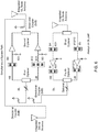
- FIG 6 illustrates an exemplary cellular signal amplifier configured with a simultaneous bypass path.
- the cellular signal amplifier can amplify downlink (DL) and uplink (UL) signals. However, the cellular signal amplifier can amplify either DL or UL signals at a given time and allow UL non-amplified signals to simultaneously bypass amplification.
- the cellular signal amplifier can detect a power level of an UL signal. The power level of the UL signal can be detected using a detector (e.g., a diode). Based on a signal power level in relation to a defined threshold, the cellular signal amplifier can determine that the UL signal does not need amplification and can bypass either a high band or low band uplink signal amplification path.
- a detector e.g., a diode
- the UL signal when the signal power level is above the defined threshold, the UL signal can bypass the high band or low band uplink signal amplification path. On the other hand, when the signal power level is below the defined threshold, the UL signal can be directed to one of the high band or low band uplink signal amplification path. In one example, DL signals can always be directed to a high band or low band downlink signal amplification path of the cellular signal amplifier.
- the integrated device antenna when the UL signal is not amplified, can be directly coupled to the integrated UL node antenna. In other words, the UL signal can be directed sent from the integrated device antenna to the integrated UL node antenna.
- the direct coupling between the integrated device antenna and the integrated UL node antenna can be achieved using a directional coupler.
- the integrated device antenna can be coupled with the integrated UL node antenna using a splitter, a circulator, a triplexer, a quadplexer, a multiplexer, or a duplexer.
- the integrated device antenna can receive an UL signal from a wireless device.
- Signal detectors can detect a power level of the UL signal.
- one or more directional couplers can be configured such that the UL signal passes directly to the integrated UL node antenna via the simultaneous bypass path.
- the UL signal can avoid passing through the high band UL signal amplification path or the low band UL signal amplification path.
- the integrated UL node antenna can transmit the unamplified UL signal to a base station.
- the one or more directional couplers can be configured such that the UL signal is directed to a first diplexer.
- the first diplexer can direct the UL signal to either the high band UL signal amplification path or the low band UL signal amplification path, which causes the UL signal to be filtered and amplified.
- the UL signal can pass through a second diplexer, and then to the integrated UL node antenna for transmission to the base station. In this example, based on the power level of the UL signal, the UL signal does not travel through the simultaneous bypass path.
- a DL signal can be received via the integrated DL node antenna.
- the DL signal can be directed to a third diplexer.
- the DL signal can be directed to a high band DL signal amplification path or a low band DL signal amplification path, and then to a fourth diplexer.
- the DL signal can travel from the fourth diplexer to the integrated device antenna for transmission to the wireless device.
- the simultaneous bypass path can increase battery life of the cellular signal amplifier by allowing UL amplification to be turned off. Further, the simultaneous bypass path can increase reliability, in the event the cellular signal amplifier malfunctions. In one example, the simultaneous bypass path can be always active. The simultaneous bypass path can operate independently of whether or not the cellular signal amplifier has failed. The simultaneous bypass path can operate independent of relays or switches to bypass the cellular signal amplifier. Additionally, because wireless propagation paths of signals from multiple antennas can constantly vary, fading margins can exceed 15dB. Therefore, by using multiple antennas, the reliability of the cellular signal amplifier can be increased.
- FIG 7 illustrates an exemplary cellular signal amplifier configured with a simultaneous bypass path.
- the cellular signal amplifier can only amplify downlink (DL) signals.
- the cellular signal amplifier can direct an uplink (UL) signal on a simultaneous bypass path, which enables the UL signal to travel directly from an integrated device antenna to an integrated UL node antenna.
- the UL signal can avoid a filtering and amplification path.
- the integrated device antenna can be directly coupled to the integrated UL node antenna.
- the direct coupling between the integrated device antenna and the integrated UL node antenna can be achieved using a directional coupler.
- the amplification of the UL signal can account for signal loss due to the directional coupler.
- SAR specific absorption rate
- a DL signal can be received via an integrated DL node antenna.
- the DL signal can be directed to a first diplexer.
- the DL signal can be directed to a high band DL signal amplification path or a low band DL signal amplification path, and then to a second diplexer.
- the DL signal can travel from the second diplexer to the integrated device antenna for transmission to a wireless device.
- the cellular signal amplifier can receive DL signals and transmit UL signals with a single integrated node antenna.
- the integrated UL node antenna and the integrated DL node antenna can be combined to form the single integrated node antenna.
- the cellular signal amplifier can include the integrated device antenna and an integrated UL/DL node antenna.
- the integrated device antenna and the integrated UL/DL node antenna can be connected via a simultaneous bypass path, which bypasses the amplification and signaling paths.
- an UL signal from the integrated device antenna can be passed to the integrated UL/DL node antenna via the simultaneous bypass path.
- a DL signal from the integrated UL/DL node antenna can be passed to the integrated device antenna via the simultaneous bypass path.
- the FCC can limit the cellular signal amplifier to a less than 9dB system gain because the cellular signal amplifier does not perform UL amplification.
- the cellular signal amplifier can include a detector that can detect an UL signal, and then determine whether to turn the DL amplification path on or off.
- the cellular signal amplifier can include an additional low noise amplifier (LNA) to reduce the noise figure.
- LNA low noise amplifier
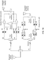
- FIG 8 illustrates an exemplary cellular signal amplifier with an amplified outside antenna and a simultaneous bypass path to a passive outside antenna.
- a modem (or inside antenna) can be coupled to the cellular signal amplifier for communication of amplified signals through the amplified outside antenna.
- the cellular signal amplifier can improve modem sensitivity, improve UL output power of the modem and improve overall performance of the modem.
- the modem can be coupled to the cellular signal amplifier when a power level of uplink (UL) or downlink (DL) signals is below a defined threshold.
- the modem can be coupled to the passive antenna for communication of non-amplified signals. These different signal paths can provide the cellular signal amplifier with signal diversity.
- the modem (or inside antenna) can be coupled to the cellular signal amplifier using a directional coupler.
- the modem can direct an UL signal to the passive outside antenna via a passive, low-loss path, and the UL signal can be transmitted using the passive outside antenna.
- the directional coupler can enable the UL signal to travel to the passive, low-loss path.
- the modem can directly send the UL signal to the passive outside antenna when a power level of the UL signal is above a defined threshold (i.e., the UL signal does not need amplification).
- the modem can direct the UL signal to a first duplexer.
- the modem can direct the UL signal to the first duplexer when the power level of the UL signal is below the defined threshold (i.e., the UL signal needs to be amplified).
- the first duplexer can direct to the UL signal through an amplifier and then to a second duplexer, which can direct the UL signal to the amplified outside antenna.
- the amplified outside antenna can receive a DL signal.
- the DL signal can be directed to the second duplexer, which can direct the DL signal to an amplifier and then to the first duplexer.
- the first duplexer can direct the DL signal to the modem (or inside antenna).
- the cellular signal amplifier can include circulators, triplexers, quadplexers, multiplexers, or splitters instead of the duplexers.
- the directional coupler can cause a 6dB gain loss in the signals transmitted across the directional coupler.
- the gain loss can be compensated with an increased gain from the cellular signal amplifier.
- the directional coupler can add some loss to the passive, low-loss path, but the loss can be minimized by an increased coupling factor.
- FIG 9 illustrates an exemplary cellular signal amplifier with a simultaneous bypass path with independent coupling for each of an amplified outside antenna and a passive outside antenna.
- the independent coupling can be achieved with a separate directional coupler for each antenna.
- a first directional coupler can be used with the amplified outside antenna
- a second directional coupler can be used with the passive outside antenna.
- the separate directional couplers can yield higher uplink (UL) to downlink (DL) signal isolation as compared to using splitters.
- a modem (or inside antenna) can direct an UL signal to the passive outside antenna via a passive, low-loss path, and the UL signal can be transmitted using the passive outside antenna.
- the first directional coupler can enable the UL signal to travel to the passive, low-loss path.
- the modem can directly send the UL signal to the passive outside antenna when a power level of the UL signal is above a defined threshold (i.e., the UL signal does not need amplification).
- the modem can direct the UL signal to an UL amplification and filtering path.
- the modem can direct the UL signal to the UL amplification and filtering path duplexer when the power level of the UL signal is below the defined threshold (i.e., the UL signal needs to be amplified).
- the first first coupler can enable the UL signal to travel to the UL amplification and filtering path.
- the UL signal can be directed via a circulator to the amplified outside antenna, which can direct the UL signal to a base station.
- the amplified outside antenna can receive a DL signal.
- the DL signal can be directed to the circulator, which can direct the DL signal to a DL amplification and filtering path. Then, the DL signal can be directed to the modem via the second directional coupler.
- the amplified and non-amplified signals can be broadcast via a single antenna.
- a single antenna can be used in place of the amplified outside antenna and the passive outside antenna.
- separate antennas can be used for UL and DL on the front end to avoid duplexer or front end losses, which can increase UL output power and DL sensitivity.
- the collisions/interference can be mitigated by signal level adjustments or delays. These adjustments can be detected and controlled using, for example, the modem.
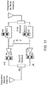
- FIG 10 illustrates an exemplary cellular signal amplifier with bypassable power amplifiers.
- An integrated device antenna can receive an uplink (UL) signal, which can be directed to a splitter, and then to a first diplexer.
- the first diplexer can direct the UL signal to a high band UL path or a low band UL path.
- the high band UL path and the low band UL path can each include a bypassable power amplifier.
- the bypassable power amplifiers are switched off (e.g., to save power)
- the UL signal from the high band UL path or the low band UL path can travel to a second diplexer, then to a third diplexer, and then to an integrated UL node antenna.
- the UL signal is not amplified to save power.
- the high band UL path and the low band UL path can each include a signal detector, which can detect a power level of the UL signal. When the power level of the UL signal is above a defined threshold, the UL signal may not be amplified.
- the UL signal from the high band UL path or the low band UL path can be directed to a respective power amplifier, and then to the third diplexer.
- the UL signal can travel from the third diplexer to the integrated UL node antenna.
- the UL signal can be amplified prior to transmission from the integrated UL node antenna.
- an integrated DL node antenna can direct a DL signal to a fourth diplexer.
- the fourth diplexer can direct the DL signal to a high band DL signal amplification and filtering path, or to a low band DL signal amplification and filtering path.
- a fifth diplexer can direct the DL signal to the splitter, which can direct the signal to the integrated device antenna.
- FIG 11 illustrates an exemplary cellular signal amplifier configured with switchable band pass filters (BPFs).
- Front end BPFs can be switched in when a weak downlink (DL) DL signal is detected or switched out when a strong DL signal is detected.
- DL downlink
- An example of a weak DL signal can be a signal with a signal strength less than -80dBm while a strong DL signal can be a signal with a signal strength greater than -80dBm.
- the minimization of noise figure can be critical in weak signal areas, and the noise figure can be reduced and the coverage extended when the front-end BPFs are switched off.
- the switchable BPFs can function to extend a receive sensitivity of the cellular signal amplifier.
- an integrated DL node antenna can receive a DL signal, and the DL signal can be provided to a first diplexer.
- the first diplexer can direct the DL signal to a high band signal amplification and filtering path, or the DL signal can be directed to a low band signal amplification and filtering path.
- the high band path and the low band path can each include switchable BPFs, which enable the DL signal to avoid passing through at least some of the BPFs.
- the DL signal can be directed to a second diplexer, and then to an integrated device antenna.
- FIG 12 illustrates an exemplary cellular signal amplifier with bypassable power amplifiers.
- the power amplifiers can be switched on when an uplink (UL) signal needs to be amplified to reach a base station or switched off and bypassed when a UL signal does not need to be amplified to reach a base station.
- the power amplifiers can be switched on when a power level of the UL signal is below a defined threshold, and the power amplifiers can be switched off when the power level of the UL signal is above the defined threshold.
- an integrated device antenna can receive an UL signal.
- the UL signal can be directed to a splitter, and then to a first diplexer.
- the first diplexer can direct the UL signal to a high band signal amplification and filtering path or a low band signal amplification and filtering path.
- Each of the high band and low band paths can include a switchable power amplifier.
- the UL signal can be provided to the power amplifier or bypass the power amplifier to save power.
- the UL signal can be provided to a second diplexer, and then to an integrated UL node antenna.
- an integrated DL node antenna can direct a DL signal to a third diplexer.
- the third diplexer can direct the DL signal to a high band DL signal amplification and filtering path, or to a low band DL signal amplification and filtering path.
- a fourth diplexer can direct the DL signal to the splitter, which can direct the signal to the integrated device antenna.
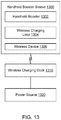
- FIG. 13 illustrates an example of a handheld booster sleeve 1300 configured to wirelessly charge a wireless device 1306 located within the handheld booster sleeve 1300.
- the handheld booster sleeve 1300 can hold a handheld booster 1302.
- the handheld booster sleeve 1300 can include a wireless charging loop 1304 and integrated circuitry to enable wireless charging in the handheld booster sleeve 1300.
- the wireless charging loop 1304 can be integrated with the handheld booster 1302.
- the wireless device 1306 By placing the wireless device 1306 with the handheld booster 1302 within the handheld booster sleeve 1300, and placing the handheld booster sleeve 1300 in proximity to a wireless charging dock 1310, the wireless device 1306 (and battery) can wirelessly charge.
- the wireless charging dock 1310 can be connected to a power source 1320, such as a wall outlet. This feature can enable wireless devices that are not configured for wireless charging to be wireless charged.
- a cellular signal booster can be configured for wireless charging.
- a cellular signal booster can be configured with a wireless charging dock, such that a wireless charging-enabled wireless device can be charged.
- Examples of the cellular signal boosters that can perform wireless charging include signal boosters found in homes, offices, and in vehicles.
- FIG. 14 provides an example illustration of the wireless device, such as a user equipment (UE), a mobile station (MS), a mobile communication device, a tablet, a handset, a wireless transceiver coupled to a processor, or other type of wireless device.
- the wireless device can include one or more antennas configured to communicate with a node or transmission station, such as an access point (AP), a base station (BS), an evolved Node B (eNB), a baseband unit (BBU), a remote radio head (RRH), a remote radio equipment (RRE), a relay station (RS), a radio equipment (RE), a remote radio unit (RRU), a central processing module (CPM), or other type of wireless wide area network (WWAN) access point.
- the wireless device can communicate using separate antennas for each wireless communication standard or shared antennas for multiple wireless communication standards.
- the wireless device can communicate in a wireless local area network (WLAN), a wireless personal area network (WPAN), and/or a WWAN.
- WLAN wireless local area network
- FIG. 14 also provides an illustration of a microphone and one or more speakers that can be used for audio input and output from the wireless device.
- the display screen can be a liquid crystal display (LCD) screen, or other type of display screen such as an organic light emitting diode (OLED) display.
- the display screen can be configured as a touch screen.
- the touch screen can use capacitive, resistive, or another type of touch screen technology.
- An application processor and a graphics processor can be coupled to internal memory to provide processing and display capabilities.
- a non-volatile memory port can also be used to provide data input/output options to a user.
- the non-volatile memory port can also be used to expand the memory capabilities of the wireless device.
- a keyboard can be with the wireless device or wirelessly connected to the wireless device to provide additional user input.
- a virtual keyboard can also be provided using the touch screen.
- Various techniques, or certain aspects or portions thereof, can take the form of program code (i.e., instructions) embodied in tangible media, such as floppy diskettes, compact disc-read-only memory (CD-ROMs), hard drives, non-transitory computer readable storage medium, or any other machine-readable storage medium wherein, when the program code is loaded into and executed by a machine, such as a computer, the machine becomes an apparatus for practicing the various techniques.
- Circuitry can include hardware, firmware, program code, executable code, computer instructions, and/or software.
- a non-transitory computer readable storage medium can be a computer readable storage medium that does not include signal.
- the computing device can include a processor, a storage medium readable by the processor (including volatile and non-volatile memory and/or storage elements), at least one input device, and at least one output device.
- the volatile and non-volatile memory and/or storage elements can be a random-access memory (RAM), erasable programmable read only memory (EPROM), flash drive, optical drive, magnetic hard drive, solid state drive, or other medium for storing electronic data.
- RAM random-access memory
- EPROM erasable programmable read only memory
- flash drive optical drive
- magnetic hard drive solid state drive
- solid state drive or other medium for storing electronic data.
- One or more programs that can implement or utilize the various techniques described herein can use an application programming interface (API), reusable controls, and the like.
- API application programming interface
- Such programs can be implemented in a high level procedural or object oriented programming language to communicate with a computer system.
- the program(s) can be implemented in assembly or machine language, if desired.
- the language can
- processor can include general purpose processors, specialized processors such as VLSI, FPGAs, or other types of specialized processors, as well as base band processors used in transceivers to send, receive, and process wireless communications.
- modules can be implemented as a hardware circuit comprising custom very-large-scale integration (VLSI) circuits or gate arrays, off-the-shelf semiconductors such as logic chips, transistors, or other discrete components.
- VLSI very-large-scale integration
- a module can also be implemented in programmable hardware devices such as field programmable gate arrays, programmable array logic, programmable logic devices or the like.
- multiple hardware circuits or multiple processors can be used to implement the functional units described in this specification.
- a first hardware circuit or a first processor can be used to perform processing operations and a second hardware circuit or a second processor (e.g., a transceiver or a baseband processor) can be used to communicate with other entities.
- the first hardware circuit and the second hardware circuit can be incorporated into a single hardware circuit, or alternatively, the first hardware circuit and the second hardware circuit can be separate hardware circuits.
- Modules can also be implemented in software for execution by various types of processors.
- An identified module of executable code can, for instance, comprise one or more physical or logical blocks of computer instructions, which can, for instance, be organized as an object, procedure, or function. Nevertheless, the executables of an identified module need not be physically located together, but can comprise disparate instructions stored in different locations which, when joined logically together, comprise the module and achieve the stated purpose for the module.
- a module of executable code can be a single instruction, or many instructions, and can even be distributed over several different code segments, among different programs, and across several memory devices.
- operational data can be identified and illustrated herein within modules, and can be embodied in any suitable form and organized within any suitable type of data structure. The operational data can be collected as a single data set, or can be distributed over different locations including over different storage devices, and can exist, at least partially, merely as electronic signals on a system or network.
- the modules can be passive or active, including agents operable to perform desired functions.
Claims (6)
- Répéteur de signal (120, 200, 310), comprenant :une antenne de dispositif (124, 322) configurée pour communiquer des signaux avec un dispositif sans fil (110) ;une antenne de noeud amplifiée configurée pour communiquer des signaux avec une station de base (130) ;une antenne de noeud passive configurée pour communiquer des signaux avec la station de base ;un ou plusieurs trajets de signaux d'amplification et de filtrage configurés pour être positionnés entre l'antenne du dispositif et l'antenne de noeud amplifiée, dans lequel les trajets de signaux d'amplification et de filtrage sont configurés pour amplifier et filtrer des signaux pour la communication vers la station de base via l'antenne de noeud amplifiée ou pour la communication vers le dispositif sans fil via l'antenne du dispositif ; etun trajet de signal de dérivation configuré pour être positionné entre l'antenne du dispositif et l'antenne du noeud passif, dans lequel le trajet de signal de dérivation n'amplifie pas et filtre les signaux passant par le trajet de signal de dérivation,caractérisé en ce que le trajet de signal de dérivation est configuré pour fonctionner simultanément avec le ou les trajets de signal d'amplification et de filtrage.
- Répéteur de signal (120, 200, 310) selon la revendication 1, comprenant en outre un ou plusieurs coupleurs directionnels utilisés pour former les trajets de signal d'amplification et de filtrage et le trajet de signal de dérivation.
- Répéteur de signal (120, 200, 310) selon la revendication 1, dans lequel :
le répéteur de signal peut être inséré dans un manchon amplificateur de signal d'appareil sans fil avec l'appareil sans fil. - Répéteur de signal (120, 200, 310) selon la revendication 1, dans lequel :
l'antenne de dispositif est une antenne de dispositif intégrée et l'antenne de noeud amplifiée est une antenne de noeud amplifiée intégrée. - Répéteur de signal (120, 200, 310) selon la revendication 1, dans lequel :les trajets de signaux d'amplification et de filtrage comprennent un trajet de signaux d'amplification et de filtrage à bande élevée pouvant être utilisé pour diriger des signaux à l'intérieur de bandes de fréquence élevée ; oules trajets de signal d'amplification et de filtrage comprennent un trajet de signal d'amplification et de filtrage à bande basse pouvant être utilisé pour diriger des signaux à l'intérieur de bandes de basse fréquence.
- Répéteur de signal (120, 200, 310) selon la revendication 1, dans lequel :
les trajets d'amplification et de filtrage des signaux sont configurés pour amplifier les signaux dans un maximum de six bandes.
Applications Claiming Priority (2)
| Application Number | Priority Date | Filing Date | Title |
|---|---|---|---|
| US201562206423P | 2015-08-18 | 2015-08-18 | |
| PCT/US2016/047549 WO2017031315A1 (fr) | 2015-08-18 | 2016-08-18 | Amplificateur de signal de dispositif sans fil |
Publications (3)
| Publication Number | Publication Date |
|---|---|
| EP3338366A1 EP3338366A1 (fr) | 2018-06-27 |
| EP3338366A4 EP3338366A4 (fr) | 2019-01-16 |
| EP3338366B1 true EP3338366B1 (fr) | 2019-12-11 |
Family
ID=58051680
Family Applications (1)
| Application Number | Title | Priority Date | Filing Date |
|---|---|---|---|
| EP16837836.2A Active EP3338366B1 (fr) | 2015-08-18 | 2016-08-18 | Amplificateur de signal de dispositif sans fil |
Country Status (5)
| Country | Link |
|---|---|
| US (3) | US9788274B2 (fr) |
| EP (1) | EP3338366B1 (fr) |
| CN (1) | CN107852223A (fr) |
| CA (2) | CA2994863C (fr) |
| WO (3) | WO2017031194A1 (fr) |
Families Citing this family (39)
| Publication number | Priority date | Publication date | Assignee | Title |
|---|---|---|---|---|
| US10862529B2 (en) | 2015-08-18 | 2020-12-08 | Wilson Electronics, Llc | Separate uplink and downlink antenna repeater architecture |
| US9788274B2 (en) * | 2015-08-18 | 2017-10-10 | Wilson Electronics, Llc | Wireless device signal amplifier |
| US10225845B2 (en) | 2015-10-14 | 2019-03-05 | Wilson Electronics, Llc | Channelization for signal boosters |
| US10715302B2 (en) | 2015-10-14 | 2020-07-14 | Wilson Electronics, Llc | Channelization for signal boosters |
| CN106411385B (zh) * | 2016-08-29 | 2020-01-10 | 西安华为技术有限公司 | 一种塔顶放大器 |
| WO2018044988A1 (fr) * | 2016-09-02 | 2018-03-08 | Cellphone-Mate, Inc. | Amplificateur de signal radiofréquence |
| WO2018057535A2 (fr) * | 2016-09-23 | 2018-03-29 | Wilson Electronics, Llc | Préamplificateur à module de système de localisation de satellite intégré |
| US10673517B2 (en) | 2016-11-15 | 2020-06-02 | Wilson Electronics, Llc | Desktop signal booster |
| US9949218B1 (en) * | 2017-02-15 | 2018-04-17 | Christopher Lau | Mobile device signal booster |
| WO2018187498A1 (fr) * | 2017-04-04 | 2018-10-11 | Wilson Electronics, Llc | Amplificateur de signaux à trajets de signaux actifs et passifs |
| CN110476371A (zh) * | 2017-04-07 | 2019-11-19 | 威尔逊电子有限责任公司 | 用于无线通信的多放大器转发器系统 |
| US10512120B2 (en) * | 2017-04-11 | 2019-12-17 | Wilson Electronics, Llc | Signal booster with coaxial cable connections |
| US10587291B2 (en) * | 2017-04-18 | 2020-03-10 | Skyworks Solutions, Inc. | Front-end architecture having split triplexer for carrier aggregation and mimo support |
| US20190196555A1 (en) * | 2017-06-16 | 2019-06-27 | Wilson Electronics, Llc | Multiple donor antenna repeater |
| US10021693B1 (en) * | 2017-08-28 | 2018-07-10 | Sprint Spectrum L.P. | Method and system for invoking uplink coverage boosting in response to threshold low power headroom and threshold low downlink receive signal strength |
| EP3460491A1 (fr) * | 2017-09-22 | 2019-03-27 | Nokia Technologies Oy | Appareil de mesure de la tension de la ligne d'alimentation d'antenne |
| US11627482B2 (en) | 2018-04-19 | 2023-04-11 | Wilson Electronics, Llc | Repeater with integrated modem for remote monitoring |
| US11252581B2 (en) * | 2018-04-24 | 2022-02-15 | Redline Communications Inc. | Bi-directional high power user equipment |
| WO2019213324A1 (fr) | 2018-05-01 | 2019-11-07 | Tunnel Radio Of America, Inc. | Système d'antenne distribué commandé à distance pour tunnels ferroviaires utilisant des amplificateurs logiciels |
| CN108923837A (zh) * | 2018-08-03 | 2018-11-30 | 佛山市苔藓云链科技有限公司 | 一种桌面信号增强器及无线设备充电站 |
| CN109168151B (zh) * | 2018-08-27 | 2021-02-09 | 丸方精密机械(上海)有限公司 | 一种便携式电子通信辅助装置 |
| US11218237B2 (en) | 2018-09-27 | 2022-01-04 | Wilson Electronics, Llc | Intermediate frequency (IF) filtering for enhanced crossover attenuation in a repeater |
| US11082194B2 (en) * | 2018-10-08 | 2021-08-03 | Actelis Networks (Israel) Ltd. | Multifunctional amplifier |
| CN111030744A (zh) | 2018-10-09 | 2020-04-17 | 威尔逊电子有限责任公司 | 基于用户设备(ue)需求的增强器增益调节 |
| US11894910B2 (en) * | 2018-12-31 | 2024-02-06 | Wilson Electronics, Llc | Cellular and public safety repeater |
| US10445726B1 (en) * | 2019-01-07 | 2019-10-15 | Capital One Services, Llc | Payment card amplification device |
| US20200383075A1 (en) * | 2019-05-29 | 2020-12-03 | Wilson Electronics, Llc | Multiplex time division duplex (tdd) sync detection module |
| WO2020247606A1 (fr) * | 2019-06-07 | 2020-12-10 | Cellphone-Mate, Inc. | Amplificateurs de signal radiofréquence servant d'infrastructure extérieure dans des réseaux cellulaires haute fréquence |
| US11979218B1 (en) | 2020-01-28 | 2024-05-07 | Cellphone-Mate, Inc. | Radio frequency signal boosters serving as outdoor infrastructure in high frequency cellular networks |
| US11742931B2 (en) * | 2020-06-26 | 2023-08-29 | Wilson Electronics, Llc | Time division duplex (TDD) network protection repeater |
| WO2022081802A1 (fr) * | 2020-10-14 | 2022-04-21 | Howell Jason T | Dispositif d'amplification de signal sans fil non alimenté |
| EP4020823A1 (fr) * | 2020-12-22 | 2022-06-29 | INTEL Corporation | Système distribué de casque radio |
| EP4020853A1 (fr) * | 2020-12-24 | 2022-06-29 | INTEL Corporation | Système de casque audio distribué |
| CN112803958B (zh) * | 2021-04-09 | 2021-08-03 | 四川科道芯国智能技术股份有限公司 | Nfc-sim系统、控制方法及移动终端 |
| CN113517918B (zh) * | 2021-04-12 | 2022-12-09 | Tcl通讯(宁波)有限公司 | 一种信号放大电路及信号放大手持移动设备 |
| US11765601B2 (en) * | 2021-09-30 | 2023-09-19 | Dell Products L.P. | Smart antenna controller system including cellular boosting functionality |
| WO2023153969A1 (fr) * | 2022-02-14 | 2023-08-17 | Telefonaktiebolaget Lm Ericsson (Publ) | Gestion de blocage de communication pour équipement utilisateur dans environnement industriel |
| CN114978272A (zh) * | 2022-04-29 | 2022-08-30 | 深圳市可信华成通信科技有限公司 | 一种多频段数字直放站 |
| CN117220699B (zh) * | 2023-11-09 | 2024-04-02 | 荣耀终端有限公司 | 一种信号增强电路、电子设备、系统及方法 |
Family Cites Families (45)
| Publication number | Priority date | Publication date | Assignee | Title |
|---|---|---|---|---|
| US4776032A (en) | 1985-05-15 | 1988-10-04 | Nippon Telegraph And Telephone Corporation | Repeater for a same frequency with spillover measurement |
| US5303395A (en) | 1991-11-06 | 1994-04-12 | Mitsubishi Consumer Electronics America, Inc. | Power control with a constant gain amplifier for portable radio transceivers |
| US5737687A (en) | 1995-03-01 | 1998-04-07 | Qualcomm Incorporated | Self-attenuating RF transceiver system using antenna and modem interfaces and cable link |
| US6005884A (en) | 1995-11-06 | 1999-12-21 | Ems Technologies, Inc. | Distributed architecture for a wireless data communications system |
| US5777530A (en) | 1996-01-31 | 1998-07-07 | Matsushita Electric Industrial Co., Ltd. | Switch attenuator |
| US5835848A (en) | 1996-12-30 | 1998-11-10 | Lucent Technologies Inc. | Range repeater for a transmission system |
| US6681100B1 (en) | 1999-03-15 | 2004-01-20 | Teletronics International, Inc. | Smart amplifier for time division duplex wireless applications |
| JP2000286652A (ja) * | 1999-03-31 | 2000-10-13 | Harada Ind Co Ltd | 制御装置 |
| US6711388B1 (en) | 2000-03-30 | 2004-03-23 | Nokia Corporation | Distributed power level control system of transmitter for cellular communication |
| US7088953B2 (en) | 2000-10-18 | 2006-08-08 | Spotwave Wireless Canada Inc. | Coverage area signature in an on-frequency repeater |
| CA2323881A1 (fr) | 2000-10-18 | 2002-04-18 | Dps Wireless Inc. | Repeteur personnel adaptatif |
| US7061993B2 (en) * | 2001-08-29 | 2006-06-13 | Sony Corporation | CDMA receiver architecture for lower bypass switch point |
| CN100440750C (zh) | 2001-11-20 | 2008-12-03 | 高通股份有限公司 | 受反向链路功率控制的中继器 |
| US6990313B1 (en) | 2002-03-14 | 2006-01-24 | Sprint Communications Company L.P. | Wireless repeater with intelligent signal display |
| WO2004002014A1 (fr) | 2002-06-21 | 2003-12-31 | Widefi, Inc. | Repeteur de reseau local sans fil |
| RU2005121147A (ru) | 2002-12-05 | 2006-01-20 | Квэлкомм Инкорпорейтед (US) | Система и способ для установки усиления обратной линии связи ретрансляторов в системах беспроводной связи |
| US20040146013A1 (en) | 2003-01-22 | 2004-07-29 | Hong Kong Applied Science And Technology Research Institute Co., Ltd | Wireless local area network time division duplex relay system with high speed automatic up-link and down-link detection |
| EP1604461A4 (fr) | 2003-02-24 | 2009-08-12 | Qualcomm Inc | Prevention des oscillations de repeteur |
| US20040166802A1 (en) | 2003-02-26 | 2004-08-26 | Ems Technologies, Inc. | Cellular signal enhancer |
| US7555261B2 (en) | 2003-03-04 | 2009-06-30 | O'neill Frank P | Repeater system for strong signal environments |
| KR20070100430A (ko) | 2003-06-30 | 2007-10-11 | 데코링크 와이어리스 엘티디. | 중계기의 알에프 출력 레벨 자동 제어 방법 |
| WO2005025078A2 (fr) | 2003-09-03 | 2005-03-17 | Behzad Mohebbi | Suramplificateur cellulaire courte portee |
| US7593689B2 (en) | 2003-09-16 | 2009-09-22 | Spotwave Wireless Inc. | Method for detecting an oscillation in an on-frequency repeater |
| US8270927B2 (en) | 2004-03-29 | 2012-09-18 | Qualcom, Incorporated | Adaptive interference filtering |
| US7221967B2 (en) | 2004-09-14 | 2007-05-22 | Wilson Electronics, Inc. | Enhanced gain selected cell phone booster system |
| US20060148401A1 (en) | 2004-12-02 | 2006-07-06 | Spotwave Wireless Canada Inc. | Method and apparatus for enabling generation of a low error timing reference for a signal received via a repeater |
| EP1982440B1 (fr) | 2006-01-27 | 2013-05-08 | QUALCOMM Incorporated | Mesure du gain en boucle ouverte d un répétiteur |
| US20080081555A1 (en) | 2006-10-03 | 2008-04-03 | Wireless Data Communication Co., Ltd | Unified communication repeater |
| US20080096483A1 (en) | 2006-10-20 | 2008-04-24 | Wilson Electronics | Power saving circuits for time division multiple access amplifiers |
| US20080161076A1 (en) | 2006-12-20 | 2008-07-03 | Lg Electronics Inc. | Case for communication terminal and communication terminal using the same |
| US7877066B2 (en) | 2007-05-07 | 2011-01-25 | Paratek Microwave Inc | Techniques to reduce the power consumption of an RF log-amp detector |
| US20090181735A1 (en) | 2008-01-02 | 2009-07-16 | Griffin Jr Paul P | Reception Boosting Accessory |
| KR101298590B1 (ko) | 2009-12-21 | 2013-08-26 | 한국전자통신연구원 | 무선 통신 시스템에서 중계 장치 및 방법 |
| US8737529B2 (en) | 2010-01-18 | 2014-05-27 | Broadcom Corporation | Multiple antenna signal transmission |
| US9037190B2 (en) * | 2011-06-14 | 2015-05-19 | Ethertronics, Inc. | Adaptive repeater for improved communication system performance |
| US20130157720A1 (en) | 2011-12-19 | 2013-06-20 | Cellvine Ltd | Tower mount amplifier and a method of using thereof |
| US9048940B2 (en) | 2012-08-31 | 2015-06-02 | Clear Rf, Llc | Passive bypass for network extending |
| WO2014036248A1 (fr) * | 2012-09-01 | 2014-03-06 | Mophie, Inc. | Accessoire de communication sans fil pour un dispositif mobile |
| US8909132B2 (en) * | 2013-03-15 | 2014-12-09 | Wilson Electronics, Llc | Bi-directional amplifier with a common amplification path |
| US8818263B1 (en) * | 2013-03-15 | 2014-08-26 | Wilson Electronics, Llc | Circuit isolation using a signal splitter/combiner |
| US8818292B1 (en) * | 2013-03-15 | 2014-08-26 | Wilson Electronics, Llc | Bi-directional amplifier with a common signal detector |
| CA2814303A1 (fr) | 2013-04-26 | 2014-10-26 | Cellphone-Mate, Inc. | Appareil et procedes pour amplificateurs de signaux de frequence radio |
| US20150029909A1 (en) * | 2013-07-25 | 2015-01-29 | Wilson Electronics, Llc | Bi-directional signal booster |
| US20160308276A1 (en) * | 2015-04-14 | 2016-10-20 | Dell Products L.P. | System and method for dynamic switching of antennas |
| US9788274B2 (en) * | 2015-08-18 | 2017-10-10 | Wilson Electronics, Llc | Wireless device signal amplifier |
-
2016
- 2016-08-17 US US15/239,384 patent/US9788274B2/en active Active
- 2016-08-17 WO PCT/US2016/047324 patent/WO2017031194A1/fr active Application Filing
- 2016-08-17 US US15/239,115 patent/US20170055214A1/en not_active Abandoned
- 2016-08-18 CA CA2994863A patent/CA2994863C/fr active Active
- 2016-08-18 CA CA2994870A patent/CA2994870A1/fr active Pending
- 2016-08-18 EP EP16837836.2A patent/EP3338366B1/fr active Active
- 2016-08-18 US US15/240,674 patent/US10251127B2/en active Active
- 2016-08-18 WO PCT/US2016/047549 patent/WO2017031315A1/fr unknown
- 2016-08-18 CN CN201680046248.9A patent/CN107852223A/zh active Pending
- 2016-08-18 WO PCT/US2016/047588 patent/WO2017031336A1/fr active Application Filing
Non-Patent Citations (1)
| Title |
|---|
| None * |
Also Published As
| Publication number | Publication date |
|---|---|
| WO2017031194A1 (fr) | 2017-02-23 |
| US20170055215A1 (en) | 2017-02-23 |
| EP3338366A1 (fr) | 2018-06-27 |
| US20170055214A1 (en) | 2017-02-23 |
| WO2017031336A1 (fr) | 2017-02-23 |
| CA2994863C (fr) | 2022-10-11 |
| US20170055231A1 (en) | 2017-02-23 |
| US9788274B2 (en) | 2017-10-10 |
| WO2017031315A1 (fr) | 2017-02-23 |
| CA2994863A1 (fr) | 2017-02-23 |
| CN107852223A (zh) | 2018-03-27 |
| US10251127B2 (en) | 2019-04-02 |
| EP3338366A4 (fr) | 2019-01-16 |
| CA2994870A1 (fr) | 2017-02-23 |
Similar Documents
| Publication | Publication Date | Title |
|---|---|---|
| EP3338366B1 (fr) | Amplificateur de signal de dispositif sans fil | |
| US10630372B2 (en) | Cellular signal booster with redundant paths for the same selected band | |
| US20230396316A1 (en) | Desktop Signal Booster | |
| CA3000535C (fr) | Amplificateur de signal | |
| US11223384B2 (en) | Low noise signal chain architecture | |
| US10873387B2 (en) | Signal booster with spectrally adjacent bands | |
| US10992371B2 (en) | Desktop signal booster | |
| CA3052456A1 (fr) | Amplificateur de signaux avec bandes spectralement adjacentes | |
| CA3052454C (fr) | Amplificateur de signal a bandes spectralement adjacentes |
Legal Events
| Date | Code | Title | Description |
|---|---|---|---|
| STAA | Information on the status of an ep patent application or granted ep patent |
Free format text: STATUS: THE INTERNATIONAL PUBLICATION HAS BEEN MADE |
|
| PUAI | Public reference made under article 153(3) epc to a published international application that has entered the european phase |
Free format text: ORIGINAL CODE: 0009012 |
|
| STAA | Information on the status of an ep patent application or granted ep patent |
Free format text: STATUS: REQUEST FOR EXAMINATION WAS MADE |
|
| 17P | Request for examination filed |
Effective date: 20180125 |
|
| AK | Designated contracting states |
Kind code of ref document: A1 Designated state(s): AL AT BE BG CH CY CZ DE DK EE ES FI FR GB GR HR HU IE IS IT LI LT LU LV MC MK MT NL NO PL PT RO RS SE SI SK SM TR |
|
| AX | Request for extension of the european patent |
Extension state: BA ME |
|
| DAV | Request for validation of the european patent (deleted) | ||
| DAX | Request for extension of the european patent (deleted) | ||
| A4 | Supplementary search report drawn up and despatched |
Effective date: 20181213 |
|
| RIC1 | Information provided on ipc code assigned before grant |
Ipc: H04W 52/52 20090101ALI20181207BHEP Ipc: H04B 7/155 20060101AFI20181207BHEP Ipc: H04W 52/02 20090101ALI20181207BHEP Ipc: H04W 88/04 20090101ALN20181207BHEP |
|
| REG | Reference to a national code |
Ref country code: DE Ref legal event code: R079 Ref document number: 602016026176 Country of ref document: DE Free format text: PREVIOUS MAIN CLASS: H03F0003213000 Ipc: H04B0007155000 |
|
| RIC1 | Information provided on ipc code assigned before grant |
Ipc: H04W 52/02 20090101ALI20190717BHEP Ipc: H04W 88/04 20090101ALN20190717BHEP Ipc: H04W 52/52 20090101ALI20190717BHEP Ipc: H04B 7/155 20060101AFI20190717BHEP |
|
| RIC1 | Information provided on ipc code assigned before grant |
Ipc: H04B 7/155 20060101AFI20190724BHEP Ipc: H04W 52/02 20090101ALI20190724BHEP Ipc: H04W 88/04 20090101ALN20190724BHEP Ipc: H04W 52/52 20090101ALI20190724BHEP |
|
| GRAP | Despatch of communication of intention to grant a patent |
Free format text: ORIGINAL CODE: EPIDOSNIGR1 |
|
| STAA | Information on the status of an ep patent application or granted ep patent |
Free format text: STATUS: GRANT OF PATENT IS INTENDED |
|
| INTG | Intention to grant announced |
Effective date: 20190923 |
|
| GRAS | Grant fee paid |
Free format text: ORIGINAL CODE: EPIDOSNIGR3 |
|
| GRAA | (expected) grant |
Free format text: ORIGINAL CODE: 0009210 |
|
| STAA | Information on the status of an ep patent application or granted ep patent |
Free format text: STATUS: THE PATENT HAS BEEN GRANTED |
|
| AK | Designated contracting states |
Kind code of ref document: B1 Designated state(s): AL AT BE BG CH CY CZ DE DK EE ES FI FR GB GR HR HU IE IS IT LI LT LU LV MC MK MT NL NO PL PT RO RS SE SI SK SM TR |
|
| REG | Reference to a national code |
Ref country code: GB Ref legal event code: FG4D |
|
| REG | Reference to a national code |
Ref country code: CH Ref legal event code: EP |
|
| REG | Reference to a national code |
Ref country code: AT Ref legal event code: REF Ref document number: 1213225 Country of ref document: AT Kind code of ref document: T Effective date: 20191215 |
|
| REG | Reference to a national code |
Ref country code: DE Ref legal event code: R096 Ref document number: 602016026176 Country of ref document: DE |
|
| REG | Reference to a national code |
Ref country code: IE Ref legal event code: FG4D |
|
| REG | Reference to a national code |
Ref country code: NL Ref legal event code: MP Effective date: 20191211 |
|
| REG | Reference to a national code |
Ref country code: LT Ref legal event code: MG4D |
|
| PG25 | Lapsed in a contracting state [announced via postgrant information from national office to epo] |
Ref country code: FI Free format text: LAPSE BECAUSE OF FAILURE TO SUBMIT A TRANSLATION OF THE DESCRIPTION OR TO PAY THE FEE WITHIN THE PRESCRIBED TIME-LIMIT Effective date: 20191211 Ref country code: NO Free format text: LAPSE BECAUSE OF FAILURE TO SUBMIT A TRANSLATION OF THE DESCRIPTION OR TO PAY THE FEE WITHIN THE PRESCRIBED TIME-LIMIT Effective date: 20200311 Ref country code: GR Free format text: LAPSE BECAUSE OF FAILURE TO SUBMIT A TRANSLATION OF THE DESCRIPTION OR TO PAY THE FEE WITHIN THE PRESCRIBED TIME-LIMIT Effective date: 20200312 Ref country code: LT Free format text: LAPSE BECAUSE OF FAILURE TO SUBMIT A TRANSLATION OF THE DESCRIPTION OR TO PAY THE FEE WITHIN THE PRESCRIBED TIME-LIMIT Effective date: 20191211 Ref country code: LV Free format text: LAPSE BECAUSE OF FAILURE TO SUBMIT A TRANSLATION OF THE DESCRIPTION OR TO PAY THE FEE WITHIN THE PRESCRIBED TIME-LIMIT Effective date: 20191211 Ref country code: SE Free format text: LAPSE BECAUSE OF FAILURE TO SUBMIT A TRANSLATION OF THE DESCRIPTION OR TO PAY THE FEE WITHIN THE PRESCRIBED TIME-LIMIT Effective date: 20191211 Ref country code: BG Free format text: LAPSE BECAUSE OF FAILURE TO SUBMIT A TRANSLATION OF THE DESCRIPTION OR TO PAY THE FEE WITHIN THE PRESCRIBED TIME-LIMIT Effective date: 20200311 |
|
| PG25 | Lapsed in a contracting state [announced via postgrant information from national office to epo] |
Ref country code: RS Free format text: LAPSE BECAUSE OF FAILURE TO SUBMIT A TRANSLATION OF THE DESCRIPTION OR TO PAY THE FEE WITHIN THE PRESCRIBED TIME-LIMIT Effective date: 20191211 Ref country code: HR Free format text: LAPSE BECAUSE OF FAILURE TO SUBMIT A TRANSLATION OF THE DESCRIPTION OR TO PAY THE FEE WITHIN THE PRESCRIBED TIME-LIMIT Effective date: 20191211 |
|
| PG25 | Lapsed in a contracting state [announced via postgrant information from national office to epo] |
Ref country code: AL Free format text: LAPSE BECAUSE OF FAILURE TO SUBMIT A TRANSLATION OF THE DESCRIPTION OR TO PAY THE FEE WITHIN THE PRESCRIBED TIME-LIMIT Effective date: 20191211 |
|
| PG25 | Lapsed in a contracting state [announced via postgrant information from national office to epo] |
Ref country code: ES Free format text: LAPSE BECAUSE OF FAILURE TO SUBMIT A TRANSLATION OF THE DESCRIPTION OR TO PAY THE FEE WITHIN THE PRESCRIBED TIME-LIMIT Effective date: 20191211 Ref country code: PT Free format text: LAPSE BECAUSE OF FAILURE TO SUBMIT A TRANSLATION OF THE DESCRIPTION OR TO PAY THE FEE WITHIN THE PRESCRIBED TIME-LIMIT Effective date: 20200506 Ref country code: EE Free format text: LAPSE BECAUSE OF FAILURE TO SUBMIT A TRANSLATION OF THE DESCRIPTION OR TO PAY THE FEE WITHIN THE PRESCRIBED TIME-LIMIT Effective date: 20191211 Ref country code: CZ Free format text: LAPSE BECAUSE OF FAILURE TO SUBMIT A TRANSLATION OF THE DESCRIPTION OR TO PAY THE FEE WITHIN THE PRESCRIBED TIME-LIMIT Effective date: 20191211 Ref country code: RO Free format text: LAPSE BECAUSE OF FAILURE TO SUBMIT A TRANSLATION OF THE DESCRIPTION OR TO PAY THE FEE WITHIN THE PRESCRIBED TIME-LIMIT Effective date: 20191211 Ref country code: NL Free format text: LAPSE BECAUSE OF FAILURE TO SUBMIT A TRANSLATION OF THE DESCRIPTION OR TO PAY THE FEE WITHIN THE PRESCRIBED TIME-LIMIT Effective date: 20191211 |
|
| PG25 | Lapsed in a contracting state [announced via postgrant information from national office to epo] |
Ref country code: SK Free format text: LAPSE BECAUSE OF FAILURE TO SUBMIT A TRANSLATION OF THE DESCRIPTION OR TO PAY THE FEE WITHIN THE PRESCRIBED TIME-LIMIT Effective date: 20191211 Ref country code: SM Free format text: LAPSE BECAUSE OF FAILURE TO SUBMIT A TRANSLATION OF THE DESCRIPTION OR TO PAY THE FEE WITHIN THE PRESCRIBED TIME-LIMIT Effective date: 20191211 Ref country code: IS Free format text: LAPSE BECAUSE OF FAILURE TO SUBMIT A TRANSLATION OF THE DESCRIPTION OR TO PAY THE FEE WITHIN THE PRESCRIBED TIME-LIMIT Effective date: 20200411 |
|
| REG | Reference to a national code |
Ref country code: DE Ref legal event code: R097 Ref document number: 602016026176 Country of ref document: DE |
|
| REG | Reference to a national code |
Ref country code: AT Ref legal event code: MK05 Ref document number: 1213225 Country of ref document: AT Kind code of ref document: T Effective date: 20191211 |
|
| PLBE | No opposition filed within time limit |
Free format text: ORIGINAL CODE: 0009261 |
|
| STAA | Information on the status of an ep patent application or granted ep patent |
Free format text: STATUS: NO OPPOSITION FILED WITHIN TIME LIMIT |
|
| PG25 | Lapsed in a contracting state [announced via postgrant information from national office to epo] |
Ref country code: DK Free format text: LAPSE BECAUSE OF FAILURE TO SUBMIT A TRANSLATION OF THE DESCRIPTION OR TO PAY THE FEE WITHIN THE PRESCRIBED TIME-LIMIT Effective date: 20191211 |
|
| 26N | No opposition filed |
Effective date: 20200914 |
|
| PG25 | Lapsed in a contracting state [announced via postgrant information from national office to epo] |
Ref country code: SI Free format text: LAPSE BECAUSE OF FAILURE TO SUBMIT A TRANSLATION OF THE DESCRIPTION OR TO PAY THE FEE WITHIN THE PRESCRIBED TIME-LIMIT Effective date: 20191211 Ref country code: AT Free format text: LAPSE BECAUSE OF FAILURE TO SUBMIT A TRANSLATION OF THE DESCRIPTION OR TO PAY THE FEE WITHIN THE PRESCRIBED TIME-LIMIT Effective date: 20191211 |
|
| PG25 | Lapsed in a contracting state [announced via postgrant information from national office to epo] |
Ref country code: IT Free format text: LAPSE BECAUSE OF FAILURE TO SUBMIT A TRANSLATION OF THE DESCRIPTION OR TO PAY THE FEE WITHIN THE PRESCRIBED TIME-LIMIT Effective date: 20191211 |
|
| PG25 | Lapsed in a contracting state [announced via postgrant information from national office to epo] |
Ref country code: PL Free format text: LAPSE BECAUSE OF FAILURE TO SUBMIT A TRANSLATION OF THE DESCRIPTION OR TO PAY THE FEE WITHIN THE PRESCRIBED TIME-LIMIT Effective date: 20191211 |
|
| PG25 | Lapsed in a contracting state [announced via postgrant information from national office to epo] |
Ref country code: MC Free format text: LAPSE BECAUSE OF FAILURE TO SUBMIT A TRANSLATION OF THE DESCRIPTION OR TO PAY THE FEE WITHIN THE PRESCRIBED TIME-LIMIT Effective date: 20191211 |
|
| REG | Reference to a national code |
Ref country code: CH Ref legal event code: PL |
|
| PG25 | Lapsed in a contracting state [announced via postgrant information from national office to epo] |
Ref country code: LU Free format text: LAPSE BECAUSE OF NON-PAYMENT OF DUE FEES Effective date: 20200818 Ref country code: LI Free format text: LAPSE BECAUSE OF NON-PAYMENT OF DUE FEES Effective date: 20200831 Ref country code: CH Free format text: LAPSE BECAUSE OF NON-PAYMENT OF DUE FEES Effective date: 20200831 |
|
| REG | Reference to a national code |
Ref country code: BE Ref legal event code: MM Effective date: 20200831 |
|
| PG25 | Lapsed in a contracting state [announced via postgrant information from national office to epo] |
Ref country code: BE Free format text: LAPSE BECAUSE OF NON-PAYMENT OF DUE FEES Effective date: 20200831 Ref country code: IE Free format text: LAPSE BECAUSE OF NON-PAYMENT OF DUE FEES Effective date: 20200818 |
|
| PG25 | Lapsed in a contracting state [announced via postgrant information from national office to epo] |
Ref country code: TR Free format text: LAPSE BECAUSE OF FAILURE TO SUBMIT A TRANSLATION OF THE DESCRIPTION OR TO PAY THE FEE WITHIN THE PRESCRIBED TIME-LIMIT Effective date: 20191211 Ref country code: MT Free format text: LAPSE BECAUSE OF FAILURE TO SUBMIT A TRANSLATION OF THE DESCRIPTION OR TO PAY THE FEE WITHIN THE PRESCRIBED TIME-LIMIT Effective date: 20191211 Ref country code: CY Free format text: LAPSE BECAUSE OF FAILURE TO SUBMIT A TRANSLATION OF THE DESCRIPTION OR TO PAY THE FEE WITHIN THE PRESCRIBED TIME-LIMIT Effective date: 20191211 |
|
| PG25 | Lapsed in a contracting state [announced via postgrant information from national office to epo] |
Ref country code: MK Free format text: LAPSE BECAUSE OF FAILURE TO SUBMIT A TRANSLATION OF THE DESCRIPTION OR TO PAY THE FEE WITHIN THE PRESCRIBED TIME-LIMIT Effective date: 20191211 |
|
| P01 | Opt-out of the competence of the unified patent court (upc) registered |
Effective date: 20230601 |
|
| PGFP | Annual fee paid to national office [announced via postgrant information from national office to epo] |
Ref country code: GB Payment date: 20230828 Year of fee payment: 8 |
|
| PGFP | Annual fee paid to national office [announced via postgrant information from national office to epo] |
Ref country code: FR Payment date: 20230825 Year of fee payment: 8 Ref country code: DE Payment date: 20230829 Year of fee payment: 8 |
|
| REG | Reference to a national code |
Ref country code: DE Ref legal event code: R082 Ref document number: 602016026176 Country of ref document: DE Representative=s name: TER MEER STEINMEISTER & PARTNER PATENTANWAELTE, DE |