EP3336895A2 - Method for fabricating damascene structure using fluorocarbon film - Google Patents
Method for fabricating damascene structure using fluorocarbon film Download PDFInfo
- Publication number
- EP3336895A2 EP3336895A2 EP17207632.5A EP17207632A EP3336895A2 EP 3336895 A2 EP3336895 A2 EP 3336895A2 EP 17207632 A EP17207632 A EP 17207632A EP 3336895 A2 EP3336895 A2 EP 3336895A2
- Authority
- EP
- European Patent Office
- Prior art keywords
- layer
- hardmask
- mask
- fluorocarbon
- dielectric
- Prior art date
- Legal status (The legal status is an assumption and is not a legal conclusion. Google has not performed a legal analysis and makes no representation as to the accuracy of the status listed.)
- Withdrawn
Links
Images


Classifications
-
- H—ELECTRICITY
- H10—SEMICONDUCTOR DEVICES; ELECTRIC SOLID-STATE DEVICES NOT OTHERWISE PROVIDED FOR
- H10D—INORGANIC ELECTRIC SEMICONDUCTOR DEVICES
- H10D89/00—Aspects of integrated devices not covered by groups H10D84/00 - H10D88/00
- H10D89/10—Integrated device layouts
-
- H—ELECTRICITY
- H10—SEMICONDUCTOR DEVICES; ELECTRIC SOLID-STATE DEVICES NOT OTHERWISE PROVIDED FOR
- H10P—GENERIC PROCESSES OR APPARATUS FOR THE MANUFACTURE OR TREATMENT OF DEVICES COVERED BY CLASS H10
- H10P14/00—Formation of materials, e.g. in the shape of layers or pillars
- H10P14/60—Formation of materials, e.g. in the shape of layers or pillars of insulating materials
- H10P14/68—Organic materials, e.g. photoresists
- H10P14/683—Organic materials, e.g. photoresists carbon-based polymeric organic materials, e.g. polyimides, poly cyclobutene or PVC
- H10P14/687—Organic materials, e.g. photoresists carbon-based polymeric organic materials, e.g. polyimides, poly cyclobutene or PVC the materials being fluorocarbon compounds, e.g. (CHxFy) n or polytetrafluoroethylene
-
- H—ELECTRICITY
- H10—SEMICONDUCTOR DEVICES; ELECTRIC SOLID-STATE DEVICES NOT OTHERWISE PROVIDED FOR
- H10P—GENERIC PROCESSES OR APPARATUS FOR THE MANUFACTURE OR TREATMENT OF DEVICES COVERED BY CLASS H10
- H10P50/00—Etching of wafers, substrates or parts of devices
- H10P50/20—Dry etching; Plasma etching; Reactive-ion etching
- H10P50/28—Dry etching; Plasma etching; Reactive-ion etching of insulating materials
- H10P50/286—Dry etching; Plasma etching; Reactive-ion etching of insulating materials of organic materials
-
- H—ELECTRICITY
- H10—SEMICONDUCTOR DEVICES; ELECTRIC SOLID-STATE DEVICES NOT OTHERWISE PROVIDED FOR
- H10P—GENERIC PROCESSES OR APPARATUS FOR THE MANUFACTURE OR TREATMENT OF DEVICES COVERED BY CLASS H10
- H10P70/00—Cleaning of wafers, substrates or parts of devices
- H10P70/20—Cleaning during device manufacture
- H10P70/27—Cleaning during device manufacture during, before or after processing of conductive materials, e.g. polysilicon or amorphous silicon layers
- H10P70/277—Cleaning during device manufacture during, before or after processing of conductive materials, e.g. polysilicon or amorphous silicon layers the processing being a planarisation of conductive layers
-
- H—ELECTRICITY
- H10—SEMICONDUCTOR DEVICES; ELECTRIC SOLID-STATE DEVICES NOT OTHERWISE PROVIDED FOR
- H10W—GENERIC PACKAGES, INTERCONNECTIONS, CONNECTORS OR OTHER CONSTRUCTIONAL DETAILS OF DEVICES COVERED BY CLASS H10
- H10W20/00—Interconnections in chips, wafers or substrates
- H10W20/01—Manufacture or treatment
- H10W20/071—Manufacture or treatment of dielectric parts thereof
- H10W20/074—Manufacture or treatment of dielectric parts thereof of dielectric parts comprising thin functional dielectric layers, e.g. dielectric etch-stop, barrier, capping or liner layers
-
- H—ELECTRICITY
- H10—SEMICONDUCTOR DEVICES; ELECTRIC SOLID-STATE DEVICES NOT OTHERWISE PROVIDED FOR
- H10W—GENERIC PACKAGES, INTERCONNECTIONS, CONNECTORS OR OTHER CONSTRUCTIONAL DETAILS OF DEVICES COVERED BY CLASS H10
- H10W20/00—Interconnections in chips, wafers or substrates
- H10W20/01—Manufacture or treatment
- H10W20/071—Manufacture or treatment of dielectric parts thereof
- H10W20/081—Manufacture or treatment of dielectric parts thereof by forming openings in the dielectric parts
- H10W20/084—Manufacture or treatment of dielectric parts thereof by forming openings in the dielectric parts for dual-damascene structures
- H10W20/087—Manufacture or treatment of dielectric parts thereof by forming openings in the dielectric parts for dual-damascene structures involving multiple stacked pre-patterned masks
-
- H—ELECTRICITY
- H10—SEMICONDUCTOR DEVICES; ELECTRIC SOLID-STATE DEVICES NOT OTHERWISE PROVIDED FOR
- H10W—GENERIC PACKAGES, INTERCONNECTIONS, CONNECTORS OR OTHER CONSTRUCTIONAL DETAILS OF DEVICES COVERED BY CLASS H10
- H10W20/00—Interconnections in chips, wafers or substrates
- H10W20/40—Interconnections external to wafers or substrates, e.g. back-end-of-line [BEOL] metallisations or vias connecting to gate electrodes
- H10W20/41—Interconnections external to wafers or substrates, e.g. back-end-of-line [BEOL] metallisations or vias connecting to gate electrodes characterised by their conductive parts
- H10W20/43—Layouts of interconnections
-
- H—ELECTRICITY
- H10—SEMICONDUCTOR DEVICES; ELECTRIC SOLID-STATE DEVICES NOT OTHERWISE PROVIDED FOR
- H10W—GENERIC PACKAGES, INTERCONNECTIONS, CONNECTORS OR OTHER CONSTRUCTIONAL DETAILS OF DEVICES COVERED BY CLASS H10
- H10W20/00—Interconnections in chips, wafers or substrates
- H10W20/40—Interconnections external to wafers or substrates, e.g. back-end-of-line [BEOL] metallisations or vias connecting to gate electrodes
- H10W20/45—Interconnections external to wafers or substrates, e.g. back-end-of-line [BEOL] metallisations or vias connecting to gate electrodes characterised by their insulating parts
- H10W20/47—Interconnections external to wafers or substrates, e.g. back-end-of-line [BEOL] metallisations or vias connecting to gate electrodes characterised by their insulating parts comprising two or more dielectric layers having different properties, e.g. different dielectric constants
-
- C—CHEMISTRY; METALLURGY
- C01—INORGANIC CHEMISTRY
- C01B—NON-METALLIC ELEMENTS; COMPOUNDS THEREOF; METALLOIDS OR COMPOUNDS THEREOF NOT COVERED BY SUBCLASS C01C
- C01B21/00—Nitrogen; Compounds thereof
- C01B21/082—Compounds containing nitrogen and non-metals and optionally metals
- C01B21/0828—Carbonitrides or oxycarbonitrides of metals, boron or silicon
-
- C—CHEMISTRY; METALLURGY
- C07—ORGANIC CHEMISTRY
- C07F—ACYCLIC, CARBOCYCLIC OR HETEROCYCLIC COMPOUNDS CONTAINING ELEMENTS OTHER THAN CARBON, HYDROGEN, HALOGEN, OXYGEN, NITROGEN, SULFUR, SELENIUM OR TELLURIUM
- C07F7/00—Compounds containing elements of Groups 4 or 14 of the Periodic Table
- C07F7/02—Silicon compounds
- C07F7/08—Compounds having one or more C—Si linkages
- C07F7/0803—Compounds with Si-C or Si-Si linkages
Definitions
- the present invention relates to semiconductor technology, and more particularly to an interconnect structure, a semiconductor device having the interconnect structure and manufacturing method thereof.
- a porous ultra-low-k material can further reduce the dielectric constant of a dielectric material in the interconnect structure, so that porous ultra-low-k materials are used in interconnect structures in smaller-sized devices.
- the present inventor has discovered that, when a porous ultra-low-k material is used as the dielectric material in an interconnect structure, the porous ultra-low-k material may be affected by other processes. For example, a planarization process may be carried out after a metal layer is filled in a formed recess and through-holes. The planarization process may introduce water into the porous ultra-low-k material, thereby affecting the dielectric properties and reliability of the interconnect structure.
- a method for manufacturing an interconnect structure includes providing a metal interconnect layer, forming a dielectric layer on the metal interconnect layer, forming a fluorocarbon layer on the dielectric layer, forming a patterned hardmask layer on the fluorocarbon layer, etching the fluorocarbon layer and the dielectric layer using the patterned hardmask layer as a mask to form a trench in the dielectric layer and a through-hole through the dielectric layer to the metal interconnect layer, forming a metal layer filling the trench and the through-hole, and planarizing the metal layer until the planarized metal layer has an upper surface that is flush with an upper surface of the fluorocarbon layer.
- the patterned hardmask layer includes a first opening extending into the hardmask layer.
- etching the fluorocarbon layer and the dielectric layer using the hardmask layer as the mask includes forming a patterned first mask layer on the hardmask layer, the patterned first mask layer having a second opening extending to a bottom of the first opening, etching the patterned hardmask layer, the fluorocarbon layer, and the dielectric layer using the first mask layer as a mask to form a third opening in the dielectric layer, removing the first mask layer, removing a portion of the dielectric layer below the third opening using the hardmask layer as a mask, and removing a portion of the hardmask layer, a portion of the fluorocarbon layer, and a portion of the dielectric layer below the first opening to form the trench and the through-hole.
- the first mask layer includes two second openings each extending to the bottom of the first opening to form two through-holes extending to the metal interconnect layer.
- forming the patterned hardmask layer on the fluorocarbon layer includes forming a first hardmask layer on the fluorocarbon layer, forming a second hardmask layer on the first hardmask layer, forming a third hardmask layer on the second hardmask layer, forming a second mask layer on the third hardmask layer, etching the third hardmask layer and the second hardmask layer using the second mask layer as a mask to form the first opening extending into the second hardmask layer or extending through the second hardmask layer to the first hardmask layer, and removing the second mask layer.
- forming the second mask layer on the third hardmask layer includes forming a mask oxide layer on the third hardmask layer, forming the second mask layer on the mask oxide layer.
- Etching the third hardmask layer and the second hardmask layer using the second mask layer as a mask includes etching the mask oxide layer, the third hardmask layer, and the second hardmask layer using the second mask layer as a mask, the method further includes, after removing the second mask layer, removing the mask oxide layer.
- the first hardmask layer includes non-porous SiOCH
- the second hardmask layer includes TEOS
- the third hardmask layer includes TiN.
- the method further includes, prior to forming the metal layer, performing a heat treatment to remove moisture in the dielectric layer.
- the heat treatment is performed at a temperature in a range between 100 °C and 400 °C, and with at least one of nitrogen gas (N 2 ), ammonia gas (NH 3 ), and hydrazine gas (N 2 H 4 ) as a protective gas.
- the method further includes forming a SiCN layer on the planarized metal layer and on the upper surface of the fluorocarbon layer.
- the dielectric layer includes a porous low-k dielectric layer.
- the dielectric layer includes a SiCN layer on the metal interconnect layer, a buffer layer on the SiCN layer, and the porous low-k dielectric layer on the buffer layer.
- the fluorocarbon layer is a hydrogen-containing fluorocarbon layer.
- the fluorocarbon layer has a thickness in a range between 5 angstroms and 1000 angstroms.
- a second aspect of the present invention provides an interconnect structure.
- the interconnect structure includes a metal interconnect layer, a dielectric layer on the metal interconnect layer, a fluorocarbon layer on the dielectric layer, a metal interconnect extending through the fluorocarbon layer and the dielectric layer to the metal interconnect layer, the metal interconnect including a first portion extending through the fluorocarbon layer and into an upper portion of the dielectric layer and a second portion below the first portion and extending through a lower portion of the dielectric layer to the metal interconnect layer.
- the second portion of the dielectric layer below the first portion includes two portions.
- the metal interconnect has an upper surface flush with an upper surface of the fluorocarbon layer.
- the interconnect structure further includes a SiCN layer on the upper surface of the metal interconnect and on the upper surface of the fluorocarbon layer.
- the dielectric layer includes a porous low-k dielectric layer.
- the dielectric layer includes a SiCN layer on the metal interconnect layer, a buffer layer on the SiCN layer, and the porous low-k dielectric layer on the buffer layer.
- the fluorocarbon layer is a hydrogen-containing fluorocarbon layer.
- the fluorocarbon layer has a thickness in a range between 5 angstroms and 1000 angstroms.
- a interconnect structure according to the first aspect of the present invention may be obtained by a method according to the second aspect of the present invention.
- Relative terms such as “below” or “above” or “upper” or “lower” or “horizontal” or “lateral” or “vertical” may be used herein to describe a relationship of one element, layer or region to another element, layer or region as illustrated in the figures. It will be understood that these terms are intended to encompass different orientations of the device in addition to the orientation depicted in the figures.
- Embodiments of the invention are described herein with reference to cross-sectional illustrations that are schematic illustrations of idealized embodiments (and intermediate structures) of the invention.
- the thickness of layers and regions in the drawings may be enlarged relative to other layers and regions for clarity. Additionally, variations from the shapes of the illustrations as a result, for example, of manufacturing techniques and/or tolerances, are to be expected.
- embodiments of the invention should not be construed as limited to the particular shapes of regions illustrated herein but are to include deviations in shapes that result, for example, from manufacturing.
- an implanted region illustrated as a rectangle will, typically, have rounded or curved features and/or a gradient of implant concentration at its edges rather than a discrete change from implanted to non-implanted region.
- a buried region formed by implantation may result in some implantation in the region between the buried region and the surface through which the implantation takes place.
- the regions illustrated in the figures are schematic in nature and their shapes are not intended to illustrate the actual shape of a region of a device and are not intended to limit the invention.
- Embodiments of the present invention propose the use of fluorocarbons to form interconnect structures.
- Fluorocarbons have good thermal stability and can withstand thermal shock in the integrated circuit manufacturing processes and increased temperature of integrated circuits during operation.
- fluorocarbons have good adhesion and good hole filling properties, and are compatible with manufacturing processes of integrated circuits.
- FIG. 1 is a simplified flowchart illustrating a method of manufacturing an interconnect structure according to an embodiment of the present invention. Referring to FIG. 1 , the method may include the following steps:
- a fluorocarbon layer is formed on a dielectric layer to prevent water from entering into the dielectric layer when planarizing a metal layer, thereby improving the reliability of the interconnect structure.
- the fluorocarbon layer may also improve the interface property between a subsequent formed barrier layer (e.g., SiCN) and the dielectric layer and mitigate or avoid plasma damage to the dielectric layer in the process of forming the SiCN barrier layer, thereby improving the reliability of the interconnect structure.
- a subsequent formed barrier layer e.g., SiCN
- FIGS. 2 to 9 are cross-sectional views illustrating intermediate stages of an interconnect structure in a manufacturing method according to some embodiments of the present invention. A manufacturing method of an interconnect structure according to some embodiments of the present invention will be described in detail with reference to FIGS. 2 to 9 .
- a metal interconnect layer 201 is provided.
- a dielectric layer 202 is formed on the metal interconnect layer.
- dielectric layer 202 may be a porous low-k or porous ultra-low-k dielectric layer having a k value less than 2.7.
- dielectric layer 202 may include a SiCN layer on metal interconnect layer 201, a buffer layer (e.g., a silicon oxide layer) on the SiCN layer, and a porous low-k or porous ultra-low-k dielectric layer on the buffer layer.
- the porous low-k or porous ultra-low-k dielectric layer may include SiOCH.
- a fluorocarbon layer 301 is formed on dielectric layer 202.
- a fluorocarbon layer may be deposited by a PECVD or PVD process using organic gases containing carbon, fluorine, and hydrogen (e.g., C x F y and CH 4 ) as a source gas.
- fluorocarbon layer 301 may be a hydrogen-containing fluorocarbon layer.
- fluorocarbon layer 301 may be a doped fluorocarbon layer, for example, the fluorocarbon layer may be doped with nitrogen or boron.
- fluorocarbon layer 301 has a thickness in the range between 5 angstroms and 1000 angstroms, e.g., e.g., 50 angstroms, 100 angstroms, 400 angstroms, 600 angstroms, etc.
- a patterned hardmask layer 401 is formed on fluorocarbon layer 301.
- patterned hardmask layer 401 has a first opening 402 extending into hardmask layer 401.
- first hardmask layer 411 is formed on fluorocarbon layer 301, a second hardmask layer 421 is formed on first hardmask layer 411, and a third hardmask layer 431 is formed on second hardmask layer 421.
- first hardmask layer 411 may include non-porous SiOCH; second hardmask layer 421 may include ethyl orthosilicate (TEOS); third hardmask layer 431 may include titanium nitride (TiN).
- TEOS ethyl orthosilicate
- third hardmask layer 431 may include titanium nitride (TiN).
- a patterned mask layer (not shown), e.g., a photoresist, is formed on third hardmask layer 431.
- first opening 402 extending through third hardmask layer 431 into second hardmask layer 421 (as shown in FIG. 4 ) or to a surface of first hardmask layer 411.
- first opening 402 may extend below the middle position relative to the upper surface of second hardmask layer 421, i.e., more than one half of the thickness of second hardmask layer 421 is removed. Thereafter, the second mask layer is removed to form first opening 402.
- first hardmask layer 411 on fluorocarbon layer 301 after sequentially forming first hardmask layer 411 on fluorocarbon layer 301, second hardmask layer 421 on first hardmask layer 411, and third hardmask layer 431 on second hardmask layer 421, a mask oxide layer (not shown), such as a silicon oxide layer, may be formed on third hardmask layer 431. Then, the second mask layer is formed on the mask oxide layer. The mask oxide layer, third mask layer 431 and second hardmask layer 421 are subsequently etched using the second mask layer as a mask. The second mask layer is then removed. Thereafter, the remaining portion of the mask oxide layer is removed to form first opening 402.
- a mask oxide layer such as a silicon oxide layer
- fluorocarbon layer 301 and dielectric layer 202 are etched using hardmask layer 401 as a mask to form a trench in dielectric layer 202 and a through-hole below the trench and extending to a surface of metal interconnect layer 201.
- opening/through-hole/trench to a layer means that the opening/through-hole/trench extends to the layer.
- the trench in dielectric layer 202 and the through-hole to metal interconnect layer 201 201 may be formed by process steps with reference to FIGS. 5 to 7 .
- a patterned mask layer 501 (also referred to as a first mask layer), e.g., a photoresist, is formed on hardmask layer 401.
- Mask layer 501 has a second opening 502 extending to the bottom of first opening 402.
- patterned mask layer 501 i.e., the first mask layer
- first mask layer 501 may have two openings 502 extending to the bottom of first opening 402 (as shown in FIG. 5 ), so that two through-holes can subsequently be formed to metal interconnect layer 201.
- first mask layer 501 may have a second opening 502 extending to the bottom of first opening 402 such that a through-hole can subsequently be formed to metal interconnect layer 201.
- hardmask layer 401, fluorocarbon layer 301, dielectric layer 202 are etched using first mask layer 501 as a mask to form a third opening 601 in dielectric layer 202. Thereafter, first mask layer 501 is removed.
- a portion of dielectric layer 202 below a remaining portion of hardmask layer 401 is removed using the remaining portion of hardmask layer 401 as a mask, and removing a portion of hardmask layer 401 (e.g., the remaining second hardmask layer 421 and first hardmask layer 411), a portion of fluorocarbon layer 301, and a portion of dielectric layer 301 below first opening 402 to form a trench 702 in dielectric layer 202 and a through-hole 701 below trench 702 and extending to metal interconnect layer 201.
- a portion of hardmask layer 401 e.g., the remaining second hardmask layer 421 and first hardmask layer 411
- the number of through-holes 701 can be any integer number. In the example shown in FIG. 7 , two through-holes 701 are used below trench 702 and extending through the remaining portion of dielectric layer 202 to metal interconnect layer 201. But it is understood that the number is arbitrary chosen for describing the example embodiment and should not be limiting. In some other embodiments, the number of through-holes 701 may be one.
- metal layer 801 is formed by deposition to fill trench 702 and through-hole 701, as shown in FIG. 8 .
- Metal layer 801 also covers a remaining portion of hardmask layer 401.
- metal layer 801 may include copper.
- a heat treatment may be performed to remove moisture from dielectric layer 202.
- a heat treatment may be performed at a temperature in the range between 100 °C and 400 °C (e.g., 200 °C, 300 °C), and with at least one of nitrogen gas (N 2 ), ammonia gas (NH 3 ), and hydrazine gas (N 2 H 4 ) as a protective gas.
- N 2 nitrogen gas
- NH 3 ammonia gas
- N 2 H 4 hydrazine gas
- metal layer 801 Next, a planarization (e.g., a chemical mechanical polishing) process is performed on metal layer 801, so that the planarized metal layer (also referred to as metal interconnect) 801 has upper surface that is substantially flush with the upper surface of the remaining portion of fluorocarbon layer 301, as shown in FIG. 9 .
- Metal interconnect 801 includes a first portion 811 and a second portion 821 below first portion 811. First portion 811 is formed by the portion of the metal layer filling the trench, and second portion 821 is formed by the portion the metal layer filling the through-hole. Fluorocarbon layer 301 on dielectric layer can prevent water from entering dielectric layer 202 in the planarization process, thereby improving the reliability of the interconnect structure.
- a SiCN barrier layer may be formed on the planarized surface of metal layer 801 and on the upper surface of fluorocarbon layer 301.
- Fluorocarbon layer 301 may also improves the interface performance between the SiCN barrier layer and dielectric layer 201 and may mitigate or avoid plasma damage to the dielectric layer in the process of forming the SiCN barrier layer, and further improve the reliability of the interconnect structure.
- FIGS. 2 to 9 A method for manufacturing an interconnect structure according to some embodiments of the present invention has been described above in connection with FIGS. 2 to 9 . It should be understood that certain steps in FIGS. 2 to 9 may be performed in different embodiments, and certain steps are not necessarily in one embodiment.
- the interconnect structure may include a metal interconnect layer 201, a dielectric layer 202 on metal interconnect layer 201, a fluorocarbon layer 301 on dielectric layer 202, and a metal interconnect 801 on metal interconnect layer 201 and extending through fluorocarbon layer 301 and dielectric layer 202.
- Metal interconnect 801 includes a first portion 811 and a second portion 821 adjacent and below first portion 811. First portion 811 extends through fluorocarbon layer 301 and an upper portion of dielectric layer 202, and second portion 821 extends through a lower portion of dielectric layer 202 and in contact with metal interconnect layer 201.
- metal interconnect 801 may include a first portion 811 and two second portion 821 disposed below first portion 811.
- a predetermined horizontal position of dielectric layer 202 is defined as a dividing line (a virtual separation line), the portion of dielectric layer 202 above the dividing line is referred to as the upper portion, and the portion of dielectric layer 202 below the dividing line is referred to as the lower portion of dielectric layer 202.
- the interconnect structure may also include a SiCN layer on metal interconnect 801 and on fluorocarbon layer 301.
Landscapes
- Internal Circuitry In Semiconductor Integrated Circuit Devices (AREA)
- Physics & Mathematics (AREA)
- Geometry (AREA)
- Engineering & Computer Science (AREA)
- General Engineering & Computer Science (AREA)
Abstract
Description
- The present application claims priority to Chinese patent application No.
201611156276.4 - The present invention relates to semiconductor technology, and more particularly to an interconnect structure, a semiconductor device having the interconnect structure and manufacturing method thereof.
- With the development of integrated circuit technology, the feature sizes of semiconductor devices are getting smaller and smaller. In order to reduce parasitic capacitance between metal interconnect lines, a low-k dielectric material is gradually used instead of silicon dioxide in the interconnect structure. A porous ultra-low-k material can further reduce the dielectric constant of a dielectric material in the interconnect structure, so that porous ultra-low-k materials are used in interconnect structures in smaller-sized devices.
- The present inventor has discovered that, when a porous ultra-low-k material is used as the dielectric material in an interconnect structure, the porous ultra-low-k material may be affected by other processes. For example, a planarization process may be carried out after a metal layer is filled in a formed recess and through-holes. The planarization process may introduce water into the porous ultra-low-k material, thereby affecting the dielectric properties and reliability of the interconnect structure.
- It is an object of the present invention to provide an interconnect structure and method for manufacturing the same that can improve the reliability of the interconnect structure.
- The object is achieved by the features of the respective independent claims. Further embodiments are defined in the respective dependent claims.
- According to a first aspect of the present invention, a method for manufacturing an interconnect structure includes providing a metal interconnect layer, forming a dielectric layer on the metal interconnect layer, forming a fluorocarbon layer on the dielectric layer, forming a patterned hardmask layer on the fluorocarbon layer, etching the fluorocarbon layer and the dielectric layer using the patterned hardmask layer as a mask to form a trench in the dielectric layer and a through-hole through the dielectric layer to the metal interconnect layer, forming a metal layer filling the trench and the through-hole, and planarizing the metal layer until the planarized metal layer has an upper surface that is flush with an upper surface of the fluorocarbon layer.
- Preferably, the patterned hardmask layer includes a first opening extending into the hardmask layer. In one embodiment, etching the fluorocarbon layer and the dielectric layer using the hardmask layer as the mask includes forming a patterned first mask layer on the hardmask layer, the patterned first mask layer having a second opening extending to a bottom of the first opening, etching the patterned hardmask layer, the fluorocarbon layer, and the dielectric layer using the first mask layer as a mask to form a third opening in the dielectric layer, removing the first mask layer, removing a portion of the dielectric layer below the third opening using the hardmask layer as a mask, and removing a portion of the hardmask layer, a portion of the fluorocarbon layer, and a portion of the dielectric layer below the first opening to form the trench and the through-hole.
- Preferably, the first mask layer includes two second openings each extending to the bottom of the first opening to form two through-holes extending to the metal interconnect layer.
- Preferably, forming the patterned hardmask layer on the fluorocarbon layer includes forming a first hardmask layer on the fluorocarbon layer, forming a second hardmask layer on the first hardmask layer, forming a third hardmask layer on the second hardmask layer, forming a second mask layer on the third hardmask layer, etching the third hardmask layer and the second hardmask layer using the second mask layer as a mask to form the first opening extending into the second hardmask layer or extending through the second hardmask layer to the first hardmask layer, and removing the second mask layer.
- Preferably, forming the second mask layer on the third hardmask layer includes forming a mask oxide layer on the third hardmask layer, forming the second mask layer on the mask oxide layer. Etching the third hardmask layer and the second hardmask layer using the second mask layer as a mask includes etching the mask oxide layer, the third hardmask layer, and the second hardmask layer using the second mask layer as a mask, the method further includes, after removing the second mask layer, removing the mask oxide layer.
- Preferably, the first hardmask layer includes non-porous SiOCH, the second hardmask layer includes TEOS, and the third hardmask layer includes TiN.
- Preferably, the method further includes, prior to forming the metal layer, performing a heat treatment to remove moisture in the dielectric layer. In one embodiment, the heat treatment is performed at a temperature in a range between 100 °C and 400 °C, and with at least one of nitrogen gas (N2), ammonia gas (NH3), and hydrazine gas (N2H4) as a protective gas.
- Preferably, the method further includes forming a SiCN layer on the planarized metal layer and on the upper surface of the fluorocarbon layer.
- Preferably, the dielectric layer includes a porous low-k dielectric layer. In one embodiment, the dielectric layer includes a SiCN layer on the metal interconnect layer, a buffer layer on the SiCN layer, and the porous low-k dielectric layer on the buffer layer.
- Preferably, the fluorocarbon layer is a hydrogen-containing fluorocarbon layer. In one embodiment, the fluorocarbon layer has a thickness in a range between 5 angstroms and 1000 angstroms.
- A second aspect of the present invention provides an interconnect structure. The interconnect structure includes a metal interconnect layer, a dielectric layer on the metal interconnect layer, a fluorocarbon layer on the dielectric layer, a metal interconnect extending through the fluorocarbon layer and the dielectric layer to the metal interconnect layer, the metal interconnect including a first portion extending through the fluorocarbon layer and into an upper portion of the dielectric layer and a second portion below the first portion and extending through a lower portion of the dielectric layer to the metal interconnect layer.
- Preferably, the second portion of the dielectric layer below the first portion includes two portions.
- Preferably, the metal interconnect has an upper surface flush with an upper surface of the fluorocarbon layer. The interconnect structure further includes a SiCN layer on the upper surface of the metal interconnect and on the upper surface of the fluorocarbon layer.
- Preferably, the dielectric layer includes a porous low-k dielectric layer. In one embodiment, the dielectric layer includes a SiCN layer on the metal interconnect layer, a buffer layer on the SiCN layer, and the porous low-k dielectric layer on the buffer layer.
- Preferably, the fluorocarbon layer is a hydrogen-containing fluorocarbon layer. In one embodiment, the fluorocarbon layer has a thickness in a range between 5 angstroms and 1000 angstroms.
- A interconnect structure according to the first aspect of the present invention may be obtained by a method according to the second aspect of the present invention.
- The following detailed description together with the accompanying drawings will provide a better understanding of the nature and advantages of the present invention.
- Embodiments of the present invention are described with reference to the accompanying drawings. In the drawings, like reference numbers may indicate identical or functionally similar elements.
-
FIG. 1 is a simplified flowchart illustrating a method of manufacturing an interconnect structure according to an embodiment of the present invention. -
FIGS. 2 to 9 are cross-sectional views illustrating intermediate stages of an interconnect structure in a manufacturing method according to some embodiments of the present invention. - Embodiments of the present invention now will be described more fully hereinafter with reference to the accompanying drawings. The invention may, however, be embodied in many different forms and should not be construed as limited to the embodiments set forth herein. Rather, these embodiments are provided so that this invention will be thorough and complete, and will fully convey the invention to those skilled in the art. The features may not be drawn to scale, some details may be exaggerated relative to other elements for clarity. Like numbers refer to like elements throughout.
- It will be understood that when an element such as a layer, region or substrate is referred to as being "on" or extending "onto" another element, it can be directly on or extend directly onto the other element or intervening elements may also be present. In contrast, when an element is referred to as being "directly on" or extending "directly onto" another element, there are no intervening elements present. It will also be understood that when an element is referred to as being "connected" or "coupled" to another element, it can be directly connected or coupled to the other element or intervening elements may be present. In contrast, when an element is referred to as being "directly connected" or "directly coupled" to another element, there are no intervening elements present.
- Relative terms such as "below" or "above" or "upper" or "lower" or "horizontal" or "lateral" or "vertical" may be used herein to describe a relationship of one element, layer or region to another element, layer or region as illustrated in the figures. It will be understood that these terms are intended to encompass different orientations of the device in addition to the orientation depicted in the figures.
- The terminology used herein is for the purpose of describing particular embodiments only and is not intended to be limiting of the invention. As used herein, the singular forms "a", "an", and "the" are intended to include the plural forms as well, unless the context clearly indicates otherwise. It will be further understood that the terms "comprises", "comprising", "includes", and/or "including" when used herein, specify the presence of stated features, integers, steps, operations, elements, and/or components, but do not preclude the presence or addition of one or more other features, integers, steps, operations, elements, components, and/or groups thereof.
- Embodiments of the invention are described herein with reference to cross-sectional illustrations that are schematic illustrations of idealized embodiments (and intermediate structures) of the invention. The thickness of layers and regions in the drawings may be enlarged relative to other layers and regions for clarity. Additionally, variations from the shapes of the illustrations as a result, for example, of manufacturing techniques and/or tolerances, are to be expected. Thus, embodiments of the invention should not be construed as limited to the particular shapes of regions illustrated herein but are to include deviations in shapes that result, for example, from manufacturing. For example, an implanted region illustrated as a rectangle will, typically, have rounded or curved features and/or a gradient of implant concentration at its edges rather than a discrete change from implanted to non-implanted region. Likewise, a buried region formed by implantation may result in some implantation in the region between the buried region and the surface through which the implantation takes place. Thus, the regions illustrated in the figures are schematic in nature and their shapes are not intended to illustrate the actual shape of a region of a device and are not intended to limit the invention.
- The embodiments described and references in the invention to "one embodiment," "an embodiment," "an exemplary embodiment" indicate that the embodiments described may include a particular feature, structure, or characteristic. However, every embodiment may not necessary include the particular feature, structure or characteristic. As used throughout this invention, the terms "depositing" and "forming" are used interchangeably.
- Embodiments of the present invention now will be described more fully hereinafter with reference to the accompanying drawings, in which embodiments of the invention are shown. This invention may, however, be embodied in many different forms and should not be construed as limited to the embodiments set forth herein.
- Embodiments of the present invention propose the use of fluorocarbons to form interconnect structures. Fluorocarbons have good thermal stability and can withstand thermal shock in the integrated circuit manufacturing processes and increased temperature of integrated circuits during operation. In addition, fluorocarbons have good adhesion and good hole filling properties, and are compatible with manufacturing processes of integrated circuits.
-
FIG. 1 is a simplified flowchart illustrating a method of manufacturing an interconnect structure according to an embodiment of the present invention. Referring toFIG. 1 , the method may include the following steps: - Step 102: providing a metal interconnect layer, and forming a dielectric layer on the metal interconnect layer. The metal interconnect layer may include copper. The dielectric layer may include a porous low-k dielectric material, e.g., SiCOH.
- Step 104: forming a fluorocarbon layer on the dielectric layer by deposition. For example, the fluorocarbon layer may be formed using a plasma enhanced chemical vapor deposition (PECVD) process or a physical vapor deposition (PVD) process. The fluorocarbon layer may include a fluorocarbon compound having a chemical structure of CxFy, where x and y are integers that vary according to different process conditions. In one embodiment, the fluorocarbon layer may include a hydrogen-containing fluorocarbon layer.
- Step 106: forming a patterned hardmask layer on the fluorocarbon layer.
- Step 108: etching the fluorocarbon layer and the dielectric layer using the patterned hardmask layer as a mask to form a trench in the dielectric layer and a through-hole below the trench and extending to the metal interconnect layer.
- Step 110: forming a metal layer by deposition to fill the trench and the through-hole. The metal layer may include copper.
- Step 112: performing a planarization (e.g., chemical mechanical polishing) process on the metal layer so that the planarized metal layer has an upper surface that is substantially flush with the upper surface of the fluorocarbon layer. As used herein, the term "the surfaces are substantially flush with each other" means that the surfaces are coplanar or flush within the process variation tolerance.
- According to embodiments of the present invention, a fluorocarbon layer is formed on a dielectric layer to prevent water from entering into the dielectric layer when planarizing a metal layer, thereby improving the reliability of the interconnect structure. Further, the fluorocarbon layer may also improve the interface property between a subsequent formed barrier layer (e.g., SiCN) and the dielectric layer and mitigate or avoid plasma damage to the dielectric layer in the process of forming the SiCN barrier layer, thereby improving the reliability of the interconnect structure.
-
FIGS. 2 to 9 are cross-sectional views illustrating intermediate stages of an interconnect structure in a manufacturing method according to some embodiments of the present invention. A manufacturing method of an interconnect structure according to some embodiments of the present invention will be described in detail with reference toFIGS. 2 to 9 . - Referring to
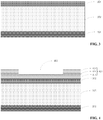
FIG. 2 , ametal interconnect layer 201 is provided. Adielectric layer 202 is formed on the metal interconnect layer. In one embodiment,dielectric layer 202 may be a porous low-k or porous ultra-low-k dielectric layer having a k value less than 2.7. In another embodiment,dielectric layer 202 may include a SiCN layer onmetal interconnect layer 201, a buffer layer (e.g., a silicon oxide layer) on the SiCN layer, and a porous low-k or porous ultra-low-k dielectric layer on the buffer layer. The porous low-k or porous ultra-low-k dielectric layer may include SiOCH. - Referring to
FIG. 3 , afluorocarbon layer 301 is formed ondielectric layer 202. For example, a fluorocarbon layer may be deposited by a PECVD or PVD process using organic gases containing carbon, fluorine, and hydrogen (e.g., CxFy and CH4) as a source gas. In one embodiment,fluorocarbon layer 301 may be a hydrogen-containing fluorocarbon layer. In one embodiment,fluorocarbon layer 301 may be a doped fluorocarbon layer, for example, the fluorocarbon layer may be doped with nitrogen or boron. In one embodiment,fluorocarbon layer 301 has a thickness in the range between 5 angstroms and 1000 angstroms, e.g., e.g., 50 angstroms, 100 angstroms, 400 angstroms, 600 angstroms, etc. - Next, referring to
FIG. 4 , a patternedhardmask layer 401 is formed onfluorocarbon layer 301. In one embodiment, patternedhardmask layer 401 has afirst opening 402 extending intohardmask layer 401. - In some embodiments, a
first hardmask layer 411 is formed onfluorocarbon layer 301, asecond hardmask layer 421 is formed onfirst hardmask layer 411, and athird hardmask layer 431 is formed onsecond hardmask layer 421. In one embodiment,first hardmask layer 411 may include non-porous SiOCH;second hardmask layer 421 may include ethyl orthosilicate (TEOS);third hardmask layer 431 may include titanium nitride (TiN). Of course, the present invention is not limited thereto. Then, a patterned mask layer (not shown), e.g., a photoresist, is formed onthird hardmask layer 431. In order to distinguish a subsequently formed first mask layer, the patterned mask layer herein is referred to as a second mask layer. Next, an etch process is performed onthird hardmask layer 431 andsecond hardmask layer 421 using the second mask layer as a mask to formfirst opening 402 extending throughthird hardmask layer 431 into second hardmask layer 421 (as shown inFIG. 4 ) or to a surface offirst hardmask layer 411. In one embodiment,first opening 402 may extend below the middle position relative to the upper surface ofsecond hardmask layer 421, i.e., more than one half of the thickness ofsecond hardmask layer 421 is removed. Thereafter, the second mask layer is removed to formfirst opening 402. - In some other embodiments, after sequentially forming
first hardmask layer 411 onfluorocarbon layer 301,second hardmask layer 421 onfirst hardmask layer 411, andthird hardmask layer 431 onsecond hardmask layer 421, a mask oxide layer (not shown), such as a silicon oxide layer, may be formed onthird hardmask layer 431. Then, the second mask layer is formed on the mask oxide layer. The mask oxide layer,third mask layer 431 andsecond hardmask layer 421 are subsequently etched using the second mask layer as a mask. The second mask layer is then removed. Thereafter, the remaining portion of the mask oxide layer is removed to formfirst opening 402. - Next,
fluorocarbon layer 301 anddielectric layer 202 are etched usinghardmask layer 401 as a mask to form a trench indielectric layer 202 and a through-hole below the trench and extending to a surface ofmetal interconnect layer 201. - It should be noted that, as used herein, the term "opening/through-hole/trench to a layer" means that the opening/through-hole/trench extends to the layer.
- In one embodiment, the trench in
dielectric layer 202 and the through-hole tometal interconnect layer 201 201 may be formed by process steps with reference toFIGS. 5 to 7 . - Referring to
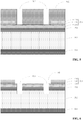
FIG. 5 , a patterned mask layer 501 (also referred to as a first mask layer), e.g., a photoresist, is formed onhardmask layer 401.Mask layer 501 has asecond opening 502 extending to the bottom offirst opening 402. In one embodiment, patterned mask layer 501 (i.e., the first mask layer) may have twoopenings 502 extending to the bottom of first opening 402 (as shown inFIG. 5 ), so that two through-holes can subsequently be formed tometal interconnect layer 201. In another embodiment,first mask layer 501 may have asecond opening 502 extending to the bottom offirst opening 402 such that a through-hole can subsequently be formed tometal interconnect layer 201. - Referring to
FIG. 6 ,hardmask layer 401,fluorocarbon layer 301,dielectric layer 202 are etched usingfirst mask layer 501 as a mask to form athird opening 601 indielectric layer 202. Thereafter,first mask layer 501 is removed. - Referring to
FIG. 7 , a portion ofdielectric layer 202 below a remaining portion ofhardmask layer 401 is removed using the remaining portion ofhardmask layer 401 as a mask, and removing a portion of hardmask layer 401 (e.g., the remainingsecond hardmask layer 421 and first hardmask layer 411), a portion offluorocarbon layer 301, and a portion ofdielectric layer 301 belowfirst opening 402 to form atrench 702 indielectric layer 202 and a through-hole 701 belowtrench 702 and extending tometal interconnect layer 201. - It is understood that the number of through-
holes 701 can be any integer number. In the example shown inFIG. 7 , two through-holes 701 are used belowtrench 702 and extending through the remaining portion ofdielectric layer 202 tometal interconnect layer 201. But it is understood that the number is arbitrary chosen for describing the example embodiment and should not be limiting. In some other embodiments, the number of through-holes 701 may be one. - After forming
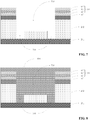
trench 702 and through-hole 701, ametal layer 801 is formed by deposition to filltrench 702 and through-hole 701, as shown inFIG. 8 .Metal layer 801 also covers a remaining portion ofhardmask layer 401. In one embodiment,metal layer 801 may include copper. - In one embodiment, prior to forming
metal layer 801, a heat treatment may be performed to remove moisture fromdielectric layer 202. In one embodiment, a heat treatment may be performed at a temperature in the range between 100 °C and 400 °C (e.g., 200 °C, 300 °C), and with at least one of nitrogen gas (N2), ammonia gas (NH3), and hydrazine gas (N2H4) as a protective gas. After the heat treatment, the moisture in the dielectric layer substantially disappears, and in the subsequent planarization process, water will not enter the dielectric layer due to the protection offluorocarbon layer 301. - Next, a planarization (e.g., a chemical mechanical polishing) process is performed on
metal layer 801, so that the planarized metal layer (also referred to as metal interconnect) 801 has upper surface that is substantially flush with the upper surface of the remaining portion offluorocarbon layer 301, as shown inFIG. 9 .Metal interconnect 801 includes afirst portion 811 and asecond portion 821 belowfirst portion 811.First portion 811 is formed by the portion of the metal layer filling the trench, andsecond portion 821 is formed by the portion the metal layer filling the through-hole.Fluorocarbon layer 301 on dielectric layer can prevent water from enteringdielectric layer 202 in the planarization process, thereby improving the reliability of the interconnect structure. - Next, in one embodiment, a SiCN barrier layer may be formed on the planarized surface of
metal layer 801 and on the upper surface offluorocarbon layer 301.Fluorocarbon layer 301 may also improves the interface performance between the SiCN barrier layer anddielectric layer 201 and may mitigate or avoid plasma damage to the dielectric layer in the process of forming the SiCN barrier layer, and further improve the reliability of the interconnect structure. - A method for manufacturing an interconnect structure according to some embodiments of the present invention has been described above in connection with
FIGS. 2 to 9 . It should be understood that certain steps inFIGS. 2 to 9 may be performed in different embodiments, and certain steps are not necessarily in one embodiment. - Embodiments of the present invention also provide an interconnect structure. Referring to
FIG. 9 , the interconnect structure may include ametal interconnect layer 201, adielectric layer 202 onmetal interconnect layer 201, afluorocarbon layer 301 ondielectric layer 202, and ametal interconnect 801 onmetal interconnect layer 201 and extending throughfluorocarbon layer 301 anddielectric layer 202.Metal interconnect 801 includes afirst portion 811 and asecond portion 821 adjacent and belowfirst portion 811.First portion 811 extends throughfluorocarbon layer 301 and an upper portion ofdielectric layer 202, andsecond portion 821 extends through a lower portion ofdielectric layer 202 and in contact withmetal interconnect layer 201. In one embodiment,metal interconnect 801 may include afirst portion 811 and twosecond portion 821 disposed belowfirst portion 811. - It is to be understood that the terms "upper portion" and "lower portion" of
dielectric layer 202 are merely conceptual. For example, a predetermined horizontal position ofdielectric layer 202 is defined as a dividing line (a virtual separation line), the portion ofdielectric layer 202 above the dividing line is referred to as the upper portion, and the portion ofdielectric layer 202 below the dividing line is referred to as the lower portion ofdielectric layer 202. - In some other embodiments, the interconnect structure may also include a SiCN layer on
metal interconnect 801 and onfluorocarbon layer 301.
Claims (15)
- A method for manufacturing an interconnect structure, the method comprising:providing a metal interconnect layer;forming a dielectric layer on the metal interconnect layer;forming a fluorocarbon layer on the dielectric layer;forming a patterned hardmask layer on the fluorocarbon layer;etching the fluorocarbon layer and the dielectric layer using the patterned hardmask layer as a mask to form a trench in the dielectric layer and a through-hole through the dielectric layer to the metal interconnect layer;forming a metal layer filling the trench and the through-hole; andplanarizing the metal layer until the planarized metal layer has an upper surface that is flush with an upper surface of the fluorocarbon layer.
- The method of claim 1, wherein the patterned hardmask layer comprises a first opening extending into the hardmask layer, and etching the fluorocarbon layer and the dielectric layer using the hardmask layer as the mask comprises:forming a patterned first mask layer on the hardmask layer, the patterned first mask layer having a second opening extending to a bottom of the first opening;etching the patterned hardmask layer, the fluorocarbon layer, and the dielectric layer using the first mask layer as a mask to form a third opening in the dielectric layer;removing the first mask layer;removing a portion of the dielectric layer below the third opening using the hardmask layer as a mask; andremoving a portion of the hardmask layer, a portion of the fluorocarbon layer, and a portion of the dielectric layer below the first opening to form the trench and the through-hole.
- The method of claim 2, wherein the first mask layer comprises two second openings each extending to the bottom of the first opening to form two through-holes extending to the metal interconnect layer.
- The method of claim 2 or 3, wherein forming the patterned hardmask layer on the fluorocarbon layer comprises:forming a first hardmask layer on the fluorocarbon layer;forming a second hardmask layer on the first hardmask layer;forming a third hardmask layer on the second hardmask layer;forming a second mask layer on the third hardmask layer;etching the third hardmask layer and the second hardmask layer using the second mask layer as a mask to form the first opening extending into the second hardmask layer or extending through the second hardmask layer to the first hardmask layer; andremoving the second mask layer.
- The method of claim 4, wherein forming the second mask layer on the third hardmask layer comprises:forming a mask oxide layer on the third hardmask layer;forming the second mask layer on the mask oxide layer; andwherein etching the third hardmask layer and the second hardmask layer using the second mask layer as a mask comprises:etching the mask oxide layer, the third hardmask layer, and the second hardmask layer using the second mask layer as a mask;the method further comprising, after removing the second mask layer:removing the mask oxide layer.
- The method of claim 4 or 5, wherein:the first hardmask layer comprises non-porous SiOCH;the second hardmask layer comprises TEOS;the third hardmask layer comprises TiN.
- The method of anyone of the claims 1-6, further comprising, prior to forming the metal layer:performing a heat treatment to remove moisture in the dielectric layer; andwherein preferably: the heat treatment is performed at a temperature in a range between 100 oC and 400 oC, and with at least one of nitrogen gas, ammonia gas, and hydrazine gas as a protective gas.
- The method of anyone of the claims 1-7, further comprising:forming a SiCN layer on the planarized metal layer and on the upper surface of the fluorocarbon layer.
- The method of anyone of the claims 1-8, wherein the dielectric layer comprises a porous low-k dielectric layer; and
wherein preferably: the dielectric layer comprises a SiCN layer on the metal interconnect layer, a buffer layer on the SiCN layer, and the porous low-k dielectric layer on the buffer layer. - The method of anyone of the claims 1-9, wherein
the fluorocarbon layer is a hydrogen-containing fluorocarbon layer; and/or
the fluorocarbon layer has a thickness in a range between 5 angstroms and 1000 angstroms. - An interconnect structure, comprising:a metal interconnect layer;a dielectric layer on the metal interconnect layer;a fluorocarbon layer on the dielectric layer;a metal interconnect extending through the fluorocarbon layer and the dielectric layer to the metal interconnect layer, the metal interconnect comprising a first portion extending through the fluorocarbon layer and into an upper portion of the dielectric layer and a second portion below the first portion and extending through a lower portion of the dielectric layer to the metal interconnect layer.
- The interconnect structure of claim 11, wherein the second portion of the dielectric layer comprises two portions.
- The interconnect structure of claim 11 or 12, wherein the metal interconnect has an upper surface flush with an upper surface of the fluorocarbon layer, the interconnect structure further comprising:a SiCN layer on the upper surface of the metal interconnect and on the upper surface of the fluorocarbon layer.
- The interconnect structure of anyone of the claims 11-13, wherein the dielectric layer comprises a porous low-k dielectric layer; and
wherein preferably: the dielectric layer comprises a SiCN layer on the metal interconnect layer, a buffer layer on the SiCN layer, and the porous low-k dielectric layer on the buffer layer. - The interconnect structure of anyone of the claims 11-14, wherein
the fluorocarbon layer is a hydrogen-containing fluorocarbon layer; and/or
the fluorocarbon layer has a thickness in a range between 5 angstroms and 1000 angstroms.
Applications Claiming Priority (1)
| Application Number | Priority Date | Filing Date | Title |
|---|---|---|---|
| CN201611156276.4A CN108231659B (en) | 2016-12-15 | 2016-12-15 | Interconnect structure and method of making the same |
Publications (2)
| Publication Number | Publication Date |
|---|---|
| EP3336895A2 true EP3336895A2 (en) | 2018-06-20 |
| EP3336895A3 EP3336895A3 (en) | 2018-07-04 |
Family
ID=60673670
Family Applications (1)
| Application Number | Title | Priority Date | Filing Date |
|---|---|---|---|
| EP17207632.5A Withdrawn EP3336895A3 (en) | 2016-12-15 | 2017-12-15 | Method for fabricating damascene structure using fluorocarbon film |
Country Status (3)
| Country | Link |
|---|---|
| US (2) | US10504883B2 (en) |
| EP (1) | EP3336895A3 (en) |
| CN (1) | CN108231659B (en) |
Families Citing this family (1)
| Publication number | Priority date | Publication date | Assignee | Title |
|---|---|---|---|---|
| CN115547979A (en) * | 2022-10-31 | 2022-12-30 | 上海积塔半导体有限公司 | Metal interconnection structure and preparation method thereof |
Family Cites Families (20)
| Publication number | Priority date | Publication date | Assignee | Title |
|---|---|---|---|---|
| JPH1154504A (en) * | 1997-08-04 | 1999-02-26 | Sony Corp | Method for forming laminated insulator film and semiconductor device using the same |
| US6291334B1 (en) * | 1997-12-19 | 2001-09-18 | Applied Materials, Inc. | Etch stop layer for dual damascene process |
| US6420261B2 (en) * | 1998-08-31 | 2002-07-16 | Fujitsu Limited | Semiconductor device manufacturing method |
| US6949203B2 (en) | 1999-12-28 | 2005-09-27 | Applied Materials, Inc. | System level in-situ integrated dielectric etch process particularly useful for copper dual damascene |
| US6541397B1 (en) * | 2002-03-29 | 2003-04-01 | Applied Materials, Inc. | Removable amorphous carbon CMP stop |
| US20030190829A1 (en) | 2002-04-05 | 2003-10-09 | Brennan Kenneth D. | Dual damascene barrier structures and preferential etching method |
| US6599838B1 (en) | 2002-07-02 | 2003-07-29 | Taiwan Semiconductor Manufacturing Co., Ltd | Method for forming metal filled semiconductor features to improve a subsequent metal CMP process |
| US7091612B2 (en) * | 2003-10-14 | 2006-08-15 | Infineon Technologies Ag | Dual damascene structure and method |
| US7129159B2 (en) * | 2004-08-17 | 2006-10-31 | International Business Machines Corporation | Integrated dual damascene RIE process with organic patterning layer |
| JP4525534B2 (en) * | 2005-09-02 | 2010-08-18 | ソニー株式会社 | Manufacturing method of semiconductor device |
| US7749894B2 (en) * | 2006-11-09 | 2010-07-06 | Chartered Semiconductor Manufacturing Ltd. | Integrated circuit processing system |
| JP2009111251A (en) * | 2007-10-31 | 2009-05-21 | Tohoku Univ | Semiconductor device and manufacturing method thereof |
| JP5143769B2 (en) * | 2008-03-12 | 2013-02-13 | 東京エレクトロン株式会社 | Semiconductor device and manufacturing method thereof |
| JP2010103329A (en) * | 2008-10-24 | 2010-05-06 | Toshiba Corp | Method of manufacturing semiconductor device, and semiconductor device |
| US8889544B2 (en) * | 2011-02-16 | 2014-11-18 | Taiwan Semiconductor Manufacturing Company, Ltd. | Dielectric protection layer as a chemical-mechanical polishing stop layer |
| CN103165514B (en) * | 2011-12-08 | 2015-07-08 | 中芯国际集成电路制造(上海)有限公司 | Semiconductor structure and forming method thereof |
| JP5930416B2 (en) * | 2011-12-28 | 2016-06-08 | 国立大学法人東北大学 | Wiring structure, semiconductor device provided with wiring structure, and method of manufacturing the semiconductor device |
| KR20140135709A (en) * | 2012-02-22 | 2014-11-26 | 도쿄엘렉트론가부시키가이샤 | Semiconductor-device manufacturing method, storage medium, and semiconductor device |
| US8551877B2 (en) * | 2012-03-07 | 2013-10-08 | Tokyo Electron Limited | Sidewall and chamfer protection during hard mask removal for interconnect patterning |
| US20150325525A1 (en) * | 2014-05-08 | 2015-11-12 | Globalfoundries Inc. | Forming interconnect structure with polymeric layer and resulting device |
-
2016
- 2016-12-15 CN CN201611156276.4A patent/CN108231659B/en active Active
-
2017
- 2017-09-29 US US15/720,734 patent/US10504883B2/en active Active
- 2017-12-15 EP EP17207632.5A patent/EP3336895A3/en not_active Withdrawn
-
2019
- 2019-11-12 US US16/681,535 patent/US11081478B2/en active Active
Non-Patent Citations (1)
| Title |
|---|
| None |
Also Published As
| Publication number | Publication date |
|---|---|
| CN108231659B (en) | 2020-07-07 |
| US20200083209A1 (en) | 2020-03-12 |
| CN108231659A (en) | 2018-06-29 |
| EP3336895A3 (en) | 2018-07-04 |
| US10504883B2 (en) | 2019-12-10 |
| US20180175015A1 (en) | 2018-06-21 |
| US11081478B2 (en) | 2021-08-03 |
Similar Documents
| Publication | Publication Date | Title |
|---|---|---|
| US7943480B2 (en) | Sub-lithographic dimensioned air gap formation and related structure | |
| US10777449B2 (en) | Methods of manufacturing semiconductor devices | |
| US9929096B2 (en) | Method for capping Cu layer using graphene in semiconductor | |
| US10181421B1 (en) | Liner recess for fully aligned via | |
| US9330964B2 (en) | Semiconductor structures and fabrication methods for improving undercut between porous film and hardmask film | |
| US11876050B2 (en) | Method for fabricating interconnection using graphene | |
| JP5263482B2 (en) | Multilayer wiring structure and method for manufacturing multilayer wiring | |
| US20190237356A1 (en) | Air gap formation in back-end-of-line structures | |
| US20160181149A1 (en) | Semiconductor structure and fabrication method thereof | |
| US20050233572A1 (en) | Dual damascene structure formed of low-k dielectric materials | |
| US10832946B1 (en) | Recessed interconnet line having a low-oxygen cap for facilitating a robust planarization process and protecting the interconnect line from downstream etch operations | |
| US20200227272A1 (en) | Interconnect Structure with Porous Low K Film | |
| CN101026122B (en) | Semiconductor device assembly and methods of manufacturing the same | |
| CN104851835A (en) | Metal interconnection structure and forming method thereof | |
| US11081478B2 (en) | Interconnect structure having a fluorocarbon layer | |
| CN103227145B (en) | Integrated circuit and for the treatment of the method with the integrated circuit imbedding feature | |
| JP5823359B2 (en) | Manufacturing method of semiconductor device | |
| JP2005005697A (en) | Manufacturing method of semiconductor device | |
| US20080057727A1 (en) | Method of manufacturing a semiconductor device | |
| JP4338748B2 (en) | Manufacturing method of semiconductor device | |
| US7541277B1 (en) | Stress relaxation, selective nitride phase removal | |
| CN103531531A (en) | Method used for manufacturing semiconductor device | |
| US20090045518A1 (en) | Semiconductor device and method for fabricating the same | |
| JP2011216828A (en) | Semiconductor device, and method of manufacturing the same |
Legal Events
| Date | Code | Title | Description |
|---|---|---|---|
| PUAI | Public reference made under article 153(3) epc to a published international application that has entered the european phase |
Free format text: ORIGINAL CODE: 0009012 |
|
| STAA | Information on the status of an ep patent application or granted ep patent |
Free format text: STATUS: THE APPLICATION HAS BEEN PUBLISHED |
|
| PUAL | Search report despatched |
Free format text: ORIGINAL CODE: 0009013 |
|
| AK | Designated contracting states |
Kind code of ref document: A2 Designated state(s): AL AT BE BG CH CY CZ DE DK EE ES FI FR GB GR HR HU IE IS IT LI LT LU LV MC MK MT NL NO PL PT RO RS SE SI SK SM TR |
|
| AX | Request for extension of the european patent |
Extension state: BA ME |
|
| AK | Designated contracting states |
Kind code of ref document: A3 Designated state(s): AL AT BE BG CH CY CZ DE DK EE ES FI FR GB GR HR HU IE IS IT LI LT LU LV MC MK MT NL NO PL PT RO RS SE SI SK SM TR |
|
| AX | Request for extension of the european patent |
Extension state: BA ME |
|
| RIC1 | Information provided on ipc code assigned before grant |
Ipc: H01L 23/532 20060101AFI20180525BHEP Ipc: H01L 21/768 20060101ALI20180525BHEP |
|
| RAP1 | Party data changed (applicant data changed or rights of an application transferred) |
Owner name: SEMICONDUCTOR MANUFACTURING INTERNATIONAL (BEIJING Owner name: SEMICONDUCTOR MANUFACTURING INTERNATIONAL (SHANGHA |
|
| STAA | Information on the status of an ep patent application or granted ep patent |
Free format text: STATUS: REQUEST FOR EXAMINATION WAS MADE |
|
| 17P | Request for examination filed |
Effective date: 20190103 |
|
| RBV | Designated contracting states (corrected) |
Designated state(s): AL AT BE BG CH CY CZ DE DK EE ES FI FR GB GR HR HU IE IS IT LI LT LU LV MC MK MT NL NO PL PT RO RS SE SI SK SM TR |
|
| STAA | Information on the status of an ep patent application or granted ep patent |
Free format text: STATUS: EXAMINATION IS IN PROGRESS |
|
| 17Q | First examination report despatched |
Effective date: 20210701 |
|
| STAA | Information on the status of an ep patent application or granted ep patent |
Free format text: STATUS: THE APPLICATION IS DEEMED TO BE WITHDRAWN |
|
| 18D | Application deemed to be withdrawn |
Effective date: 20211112 |