EP3336863A1 - Electrical device with flexible connectors - Google Patents
Electrical device with flexible connectors Download PDFInfo
- Publication number
- EP3336863A1 EP3336863A1 EP17207726.5A EP17207726A EP3336863A1 EP 3336863 A1 EP3336863 A1 EP 3336863A1 EP 17207726 A EP17207726 A EP 17207726A EP 3336863 A1 EP3336863 A1 EP 3336863A1
- Authority
- EP
- European Patent Office
- Prior art keywords
- flexible
- interconnect
- electrical device
- flexible connector
- connector
- Prior art date
- Legal status (The legal status is an assumption and is not a legal conclusion. Google has not performed a legal analysis and makes no representation as to the accuracy of the status listed.)
- Pending
Links
Images


Classifications
-
- H—ELECTRICITY
- H01—ELECTRIC ELEMENTS
- H01F—MAGNETS; INDUCTANCES; TRANSFORMERS; SELECTION OF MATERIALS FOR THEIR MAGNETIC PROPERTIES
- H01F17/00—Fixed inductances of the signal type
- H01F17/04—Fixed inductances of the signal type with magnetic core
- H01F17/06—Fixed inductances of the signal type with magnetic core with core substantially closed in itself, e.g. toroid
- H01F17/062—Toroidal core with turns of coil around it
-
- H—ELECTRICITY
- H01—ELECTRIC ELEMENTS
- H01F—MAGNETS; INDUCTANCES; TRANSFORMERS; SELECTION OF MATERIALS FOR THEIR MAGNETIC PROPERTIES
- H01F27/00—Details of transformers or inductances, in general
- H01F27/28—Coils; Windings; Conductive connections
- H01F27/2804—Printed windings
-
- H—ELECTRICITY
- H01—ELECTRIC ELEMENTS
- H01F—MAGNETS; INDUCTANCES; TRANSFORMERS; SELECTION OF MATERIALS FOR THEIR MAGNETIC PROPERTIES
- H01F27/00—Details of transformers or inductances, in general
- H01F27/28—Coils; Windings; Conductive connections
- H01F27/2895—Windings disposed upon ring cores
-
- H—ELECTRICITY
- H01—ELECTRIC ELEMENTS
- H01F—MAGNETS; INDUCTANCES; TRANSFORMERS; SELECTION OF MATERIALS FOR THEIR MAGNETIC PROPERTIES
- H01F27/00—Details of transformers or inductances, in general
- H01F27/28—Coils; Windings; Conductive connections
- H01F27/29—Terminals; Tapping arrangements for signal inductances
-
- H—ELECTRICITY
- H01—ELECTRIC ELEMENTS
- H01F—MAGNETS; INDUCTANCES; TRANSFORMERS; SELECTION OF MATERIALS FOR THEIR MAGNETIC PROPERTIES
- H01F27/00—Details of transformers or inductances, in general
- H01F27/28—Coils; Windings; Conductive connections
- H01F27/2804—Printed windings
- H01F2027/2814—Printed windings with only part of the coil or of the winding in the printed circuit board, e.g. the remaining coil or winding sections can be made of wires or sheets
-
- H—ELECTRICITY
- H01—ELECTRIC ELEMENTS
- H01F—MAGNETS; INDUCTANCES; TRANSFORMERS; SELECTION OF MATERIALS FOR THEIR MAGNETIC PROPERTIES
- H01F27/00—Details of transformers or inductances, in general
- H01F27/28—Coils; Windings; Conductive connections
- H01F27/2866—Combination of wires and sheets
-
- H—ELECTRICITY
- H01—ELECTRIC ELEMENTS
- H01F—MAGNETS; INDUCTANCES; TRANSFORMERS; SELECTION OF MATERIALS FOR THEIR MAGNETIC PROPERTIES
- H01F27/00—Details of transformers or inductances, in general
- H01F27/28—Coils; Windings; Conductive connections
- H01F27/29—Terminals; Tapping arrangements for signal inductances
- H01F27/292—Surface mounted devices
Definitions
- the subject matter disclosed herein relates to electrical devices, and more particularly, to electrical devices that utilize flexible connectors.
- Transformers and inductors are utilized in many applications to convert power and filter input and output signals.
- Transformers and inductors require numerous electrical conductors in a desired arrangement to provide the desired functionality. Often, creating and arranging the numerous electrical conductors is expensive and difficult.
- an electrical device includes a first flexible connector, including a first flexible conductor and a second flexible conductor, and a flexible insulator disposed between the first flexible conductor and the second flexible conductor, a second flexible connector spaced apart from the first flexible connector, the second flexible connector including a third flexible conductor, a first interconnect to electrically connect the first flexible conductor and the third flexible conductor, a second interconnect to electrically connect the third flexible conductor and the second flexible conductor, wherein the second interconnect is opposite the first interconnect.
- an electrical device includes a first printed wiring board including a first interconnect, a second printed wiring board including a second interconnect, a first flexible connector disposed between the first printed wiring board and the second printed wiring board, the first flexible connector including a first flexible conductor and a second flexible conductor, and a flexible insulator disposed between the first flexible conductor and the second flexible conductor, a second flexible connector spaced apart from the first flexible connector and disposed between the first printed wiring board and the second printed wiring board, the second flexible connector including a third flexible conductor, wherein the first interconnect electrically connects the first flexible conductor and the third flexible conductor, and the second interconnect electrically connects the third flexible conductor and the second flexible conductor, wherein the second interconnect is opposite the first interconnect.
- FIGS. 1A-1C show an electrical device assembly 100.
- the electrical device assembly 100 includes a lower printed wiring board 102, an upper printed wiring board 104, and a connector assembly 110.
- the electrical device assembly 100 can be configured to operate as an inductor, transformer, etc.
- the electrical device assembly 100 is shown as an inductor to filter input and output signals.
- the use of the connector assembly 110 allows for electrical connections needed for operation to be simplified.
- the electrical device assembly 100 allows for electrical connections to be formed in a desired arrangement.
- the electrical device assembly 100 includes insulation barriers 114, an outer flexible connector 116a, a device core 112, and an inner flexible connector 116b.
- the electrical device assembly 100 can be any suitable shape, including, but not limited to toroid shaped, etc.
- the outer flexible connector 116a and the inner flexible connector 116b are spaced apart with a device core 112 disposed therebetween.
- the device core 112 is a solid core formed from any suitable material, including, but not limited to ferromagnetic materials.
- the device core 112 is an air core.
- insulation barriers 114 can be disposed around the outer flexible connector 116a and the inner flexible connector 116b to prevent unintended electrical connections within the electrical device assembly 100 and provide structural support.
- each of the flexible connectors includes alternating flexible conductors 117a and flexible insulators 117b.
- the flexible connector 116 provides a unitary body containing a plurality of flexible conductors 117a, allowing for conductive paths to be selectively created as desired quickly and inexpensively. Further, by utilizing flexible conductors 117a and flexible insulators 117b, the flexible connector 116 can withstand vibrations.
- the electrical device assembly 100 is disposed between the lower printed wiring board 102 and the upper wiring board 104.
- the printed wiring boards 102,104 support and facilitate electrical connections through the electrical device assembly 100 to allow functionality as an inductor, transformer, etc.
- the lower printed wiring board 102 is shown.
- the lower printed wiring board 102 includes contact pads 105, interconnects 106, and input/output traces 108.
- the lower printed wiring board 102 is formed from any suitable printed wiring board material 103, including, but not limited to copper sheets laminated onto a non-conductive substrate.
- conductive interconnects 106 can be formed within the lower printed wiring board 102.
- the conductive interconnects 106 can be copper conductive pathways.
- the interconnects 106 are embedded within the lower printed wiring board 102 and are otherwise insulated.
- ends of the interconnect 106 include contact pads 105 that are formed on the surface of the lower printed wiring board 102.
- the interconnect 106 allows electrical contact between one contact pad 105 and the opposite contact pad 105 on the opposite end of the interconnect 106.
- the contact pads 105 and the interconnects 106 allow for electrical contact between conductors of the outer flexible connector 116a and the inner flexible connector 116b.
- the contact pads 105 are aligned with the conductors within the flexible connectors 116a, 116b to allow electrical contact between the conductors within the outer flexible connector 116a and the inner flexible connector 116b.
- input/output traces 108 can provide electricity into and out of the electrical device assembly 100.
- the input/output traces 108 are electrically connected to select interconnects 106 to allow for electricity to flow through a desired path through the connector assembly 110.
- the upper printed wiring board 104 is shown.
- the upper printed wiring board 104 includes contact pads 105 and interconnects 106.
- the upper printed wiring board 104 is formed from any suitable printed wiring board material 103, including, but not limited to copper sheets laminated onto a non-conductive substrate.
- conductive interconnects 106 can be formed within the upper printed wiring board 104.
- the conductive interconnects 106 can be copper conductive pathways.
- the interconnects 106 are embedded within the upper printed wiring board 104 and are otherwise insulated.
- ends of the interconnect 106 include contact pads 105 that are formed on the surface of the upper printed wiring board 104.
- the contact pads 105 allow electrical contact between one contact pad 105 and the opposite contact pad 105 on the opposite end of the interconnect 106.
- the contact pads 105 and the interconnects 106 allow for electrical contact between conductors within the outer flexible connector 116a and the inner flexible connector 116b.
- the contact pads 105 are aligned with the conductors within the flexible connectors 116a, 116b to allow electrical contact between the conductors within the outer flexible connector 116a and the inner flexible connector 116b.
- the lower printed wiring board 102 and the upper printed wiring board 104 facilitate desired electrical connections through the flexible connectors 116a,116b to allow the electrical device assembly 100 to function as desired.
- the configuration of the lower printed wiring board 102, the upper printed wiring board 104, and the flexible connectors 116a, 116b allows for a coiled electrical path to allow for functionality as an inductor.
- electrical current can flow into the electrical device assembly 100 via the input/output trace 108, wherein the input/output trace 108 is connected to an interconnect 106 (I Lower ) disposed within the lower printed wiring board 102.
- the contact pad 105 and the interconnect 106 (I Lower ) are aligned within the lower printed wiring board 102 with the outer flexible connector 116a to allow a flexible conductor 117a ( FIG. 4 ) (C Outer1 ) of the outer flexible conductor 116a to be electrically connected to the interconnect 106 (I Lower ) within the lower printed wiring board 102.
- the interconnect 106 (I Lower ) is further electrically connected to the opposite contact pad 105, wherein the opposite contact pad 105 is aligned with a flexible conductor 117a (C Inner1 ) of the inner flexible connector 116b.
- the contact pad 105 and the interconnect 106 (I Upper ) within the upper printed wiring board 104 are aligned with the inner flexible connector 116b to allow the flexible conductor 117a ( FIG. 4 ) (C Inner1 ) to be electrically connected to the interconnect 106 (I Upper ) within the upper printed wiring board 104.
- the interconnect 106 (I Upper ) is electrically connected with the opposite contact pad 105, wherein the opposite contact pad 105 is aligned with the next or adjacent flexible conductor 117a (C Outer2 ) of the outer flexible connector 116a.
- this allows for a coil type power flow path without expensive and complex wiring configurations. In other embodiments, any suitable power flow path configuration can be utilized.
- an electrical device assembly 200 is shown.
- the electrical device assembly 200 is similar to the electrical device assembly 100 described herein, but further includes additional flexible connectors 116c, 116d.
- the additional flexible connectors 116c, 116d can be utilized to provide additional current flow paths or to provide additional current capability.
- the flexible connector 116c can be wired in parallel with the outer flexible connector 116a to provide additional current capability.
- the flexible connector 116d can be wired in parallel with the inner flexible connector 116b.
- the flexible connector 116c can be wired in series with the outer flexible connector 116a to provide additional looping current paths.
- the flexible connector 116d can be wired in series with the inner flexible connector 116b.
- the flexible connectors 116c, 116d can be wired in any suitable configuration.
Landscapes
- Engineering & Computer Science (AREA)
- Power Engineering (AREA)
- Microelectronics & Electronic Packaging (AREA)
- Coils Of Transformers For General Uses (AREA)
- Details Of Connecting Devices For Male And Female Coupling (AREA)
- Coupling Device And Connection With Printed Circuit (AREA)
Abstract
Description
- The subject matter disclosed herein relates to electrical devices, and more particularly, to electrical devices that utilize flexible connectors.
- Electrical devices such as transformers and inductors are utilized in many applications to convert power and filter input and output signals. Transformers and inductors require numerous electrical conductors in a desired arrangement to provide the desired functionality. Often, creating and arranging the numerous electrical conductors is expensive and difficult.
- According to an embodiment, an electrical device includes a first flexible connector, including a first flexible conductor and a second flexible conductor, and a flexible insulator disposed between the first flexible conductor and the second flexible conductor, a second flexible connector spaced apart from the first flexible connector, the second flexible connector including a third flexible conductor, a first interconnect to electrically connect the first flexible conductor and the third flexible conductor, a second interconnect to electrically connect the third flexible conductor and the second flexible conductor, wherein the second interconnect is opposite the first interconnect.
- According to an embodiment an electrical device includes a first printed wiring board including a first interconnect, a second printed wiring board including a second interconnect, a first flexible connector disposed between the first printed wiring board and the second printed wiring board, the first flexible connector including a first flexible conductor and a second flexible conductor, and a flexible insulator disposed between the first flexible conductor and the second flexible conductor, a second flexible connector spaced apart from the first flexible connector and disposed between the first printed wiring board and the second printed wiring board, the second flexible connector including a third flexible conductor, wherein the first interconnect electrically connects the first flexible conductor and the third flexible conductor, and the second interconnect electrically connects the third flexible conductor and the second flexible conductor, wherein the second interconnect is opposite the first interconnect.
- Technical function of the embodiments described above includes a first interconnect to electrically connect the first flexible conductor and the third flexible conductor, a second interconnect to electrically connect the third flexible conductor and the second flexible conductor, wherein the second interconnect is opposite the first interconnect.
- Other aspects, features, and techniques of the embodiments will become more apparent from the following description taken in conjunction with the drawings.
- The subject matter is particularly pointed out and distinctly claimed in the claims at the conclusion of the specification. The foregoing and other features, and advantages of the embodiments are apparent from the following detailed description taken in conjunction with the accompanying drawings in which like elements are numbered alike in the FIGURES:
-
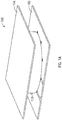
FIG. 1A is an isometric view of an embodiment of an electrical device assembly; - FIG. IB is an isometric view of the electrical device assembly of
FIG. 1A with the upper printed wiring board removed; -
FIG. 1C is a cross sectional view of the electrical device assembly ofFIG. 1A ; -
FIG. 2 is an isometric view of a lower printed wiring board for use with the electrical device assembly ofFIG. 1A ; -
FIG. 3 is an isometric view of an upper printed wiring board for use with the electrical device assembly ofFIG. 1A ; -
FIG. 4 is an isometric view of a flexible connector for use with the electrical device assembly ofFIG. 1A ; and -
FIG. 5 is a cross sectional view of an embodiment of an electrical device assembly. - Referring to the drawings,
FIGS. 1A-1C show anelectrical device assembly 100. In the illustrated embodiment, theelectrical device assembly 100 includes a lower printedwiring board 102, an upper printedwiring board 104, and aconnector assembly 110. In the illustrated embodiment, theelectrical device assembly 100 can be configured to operate as an inductor, transformer, etc. In the illustrated embodiment, theelectrical device assembly 100 is shown as an inductor to filter input and output signals. Advantageously, the use of theconnector assembly 110 allows for electrical connections needed for operation to be simplified. - In the illustrated embodiment, the
electrical device assembly 100 allows for electrical connections to be formed in a desired arrangement. In the illustrated embodiment, theelectrical device assembly 100 includesinsulation barriers 114, an outerflexible connector 116a, adevice core 112, and an innerflexible connector 116b. In the illustrated embodiment, theelectrical device assembly 100 can be any suitable shape, including, but not limited to toroid shaped, etc. - In the illustrated embodiment, the outer
flexible connector 116a and the innerflexible connector 116b are spaced apart with adevice core 112 disposed therebetween. In the illustrated embodiment, thedevice core 112 is a solid core formed from any suitable material, including, but not limited to ferromagnetic materials. In certain embodiments, thedevice core 112 is an air core. Further, in the illustrated embodiment,insulation barriers 114 can be disposed around the outerflexible connector 116a and the innerflexible connector 116b to prevent unintended electrical connections within theelectrical device assembly 100 and provide structural support. - In the illustrated embodiment, electricity can flow within the
flexible connectors FIG. 4 , each of the flexible connectors, generally referred to asflexible connector 116, includes alternatingflexible conductors 117a andflexible insulators 117b. Advantageously, theflexible connector 116 provides a unitary body containing a plurality offlexible conductors 117a, allowing for conductive paths to be selectively created as desired quickly and inexpensively. Further, by utilizingflexible conductors 117a andflexible insulators 117b, theflexible connector 116 can withstand vibrations. - Referring back to
FIGS. 1A-1C , theelectrical device assembly 100 is disposed between the lower printedwiring board 102 and theupper wiring board 104. In the illustrated embodiment, the printed wiring boards 102,104 support and facilitate electrical connections through theelectrical device assembly 100 to allow functionality as an inductor, transformer, etc. - Referring to
FIGS. 1A-2 , the lower printedwiring board 102 is shown. In the illustrated embodiment, the lower printedwiring board 102 includescontact pads 105,interconnects 106, and input/output traces 108. In the illustrated embodiment, the lower printedwiring board 102 is formed from any suitable printedwiring board material 103, including, but not limited to copper sheets laminated onto a non-conductive substrate. - In the illustrated embodiment,
conductive interconnects 106 can be formed within the lower printedwiring board 102. Theconductive interconnects 106 can be copper conductive pathways. In the illustrated embodiment, theinterconnects 106 are embedded within the lower printedwiring board 102 and are otherwise insulated. In the illustrated embodiment, ends of theinterconnect 106 includecontact pads 105 that are formed on the surface of the lower printedwiring board 102. In the illustrated embodiment, theinterconnect 106 allows electrical contact between onecontact pad 105 and theopposite contact pad 105 on the opposite end of theinterconnect 106. In the illustrated embodiment, thecontact pads 105 and theinterconnects 106 allow for electrical contact between conductors of the outerflexible connector 116a and the innerflexible connector 116b. - In the illustrated embodiment, the
contact pads 105 are aligned with the conductors within theflexible connectors flexible connector 116a and the innerflexible connector 116b. - In the illustrated embodiment, input/
output traces 108 can provide electricity into and out of theelectrical device assembly 100. In the illustrated embodiment, the input/output traces 108 are electrically connected toselect interconnects 106 to allow for electricity to flow through a desired path through theconnector assembly 110. - Referring to
FIGS 1A-C andFIG. 3 , the upper printedwiring board 104 is shown. In the illustrated embodiment, the upper printedwiring board 104 includescontact pads 105 andinterconnects 106. In the illustrated embodiment, the upper printedwiring board 104 is formed from any suitable printedwiring board material 103, including, but not limited to copper sheets laminated onto a non-conductive substrate. - In the illustrated embodiment,
conductive interconnects 106 can be formed within the upper printedwiring board 104. Theconductive interconnects 106 can be copper conductive pathways. In the illustrated embodiment, theinterconnects 106 are embedded within the upper printedwiring board 104 and are otherwise insulated. In the illustrated embodiment, ends of theinterconnect 106 includecontact pads 105 that are formed on the surface of the upper printedwiring board 104. In the illustrated embodiment, thecontact pads 105 allow electrical contact between onecontact pad 105 and theopposite contact pad 105 on the opposite end of theinterconnect 106. In the illustrated embodiment, thecontact pads 105 and theinterconnects 106 allow for electrical contact between conductors within the outerflexible connector 116a and the innerflexible connector 116b. - In the illustrated embodiment, the
contact pads 105 are aligned with the conductors within theflexible connectors flexible connector 116a and the innerflexible connector 116b. - Referring to
FIG. 1C , in the illustrated embodiment, the lower printedwiring board 102 and the upper printedwiring board 104 facilitate desired electrical connections through theflexible connectors electrical device assembly 100 to function as desired. In the illustrated embodiment, the configuration of the lower printedwiring board 102, the upper printedwiring board 104, and theflexible connectors - For example, in the illustrated embodiment, electrical current can flow into the
electrical device assembly 100 via the input/output trace 108, wherein the input/output trace 108 is connected to an interconnect 106 (ILower) disposed within the lower printedwiring board 102. In the illustrated embodiment, thecontact pad 105 and the interconnect 106 (ILower) are aligned within the lower printedwiring board 102 with the outerflexible connector 116a to allow aflexible conductor 117a (FIG. 4 ) (COuter1) of the outerflexible conductor 116a to be electrically connected to the interconnect 106 (ILower) within the lower printedwiring board 102. In the illustrated embodiment, the interconnect 106 (ILower) is further electrically connected to theopposite contact pad 105, wherein theopposite contact pad 105 is aligned with aflexible conductor 117a (CInner1) of the innerflexible connector 116b. - Similarly, in the illustrated embodiment, the
contact pad 105 and the interconnect 106 (IUpper) within the upper printedwiring board 104 are aligned with the innerflexible connector 116b to allow theflexible conductor 117a (FIG. 4 ) (CInner1) to be electrically connected to the interconnect 106 (IUpper) within the upper printedwiring board 104. In the illustrated embodiment, the interconnect 106 (IUpper) is electrically connected with theopposite contact pad 105, wherein theopposite contact pad 105 is aligned with the next or adjacentflexible conductor 117a (COuter2) of the outerflexible connector 116a. Advantageously, this allows for a coil type power flow path without expensive and complex wiring configurations. In other embodiments, any suitable power flow path configuration can be utilized. - Referring to
FIG. 5 , in the illustrated embodiment, anelectrical device assembly 200 is shown. In the illustrated embodiment, theelectrical device assembly 200 is similar to theelectrical device assembly 100 described herein, but further includes additionalflexible connectors flexible connectors flexible connector 116c can be wired in parallel with the outerflexible connector 116a to provide additional current capability. Similarly, theflexible connector 116d can be wired in parallel with the innerflexible connector 116b. In certain embodiments, theflexible connector 116c can be wired in series with the outerflexible connector 116a to provide additional looping current paths. Similarly, theflexible connector 116d can be wired in series with the innerflexible connector 116b. In other embodiments, theflexible connectors - The terminology used herein is for the purpose of describing particular embodiments only and is not intended to be limiting of the embodiments. While the description of the present embodiments has been presented for purposes of illustration and description, it is not intended to be exhaustive or limited to the embodiments in the form disclosed. Many modifications, variations, alterations, substitutions or equivalent arrangement not hereto described will be apparent to those of ordinary skill in the art without departing from the scope of the invention as defined by the claims. Additionally, while various embodiments have been described, it is to be understood that aspects may include only some of the described embodiments. Accordingly, the embodiments are not to be seen as limited by the foregoing description, but are only limited by the scope of the appended claims.
Claims (15)
- An electrical device, comprising:a first flexible connector (116a), including:a first flexible conductor (117a) and a second flexible conductor (117a); anda flexible insulator (117b) disposed between the first flexible conductor and the second flexible conductor;a second flexible connector (116b) spaced apart from the first flexible connector, the second flexible connector including a third flexible conductor;a first interconnect (106) to electrically connect the first flexible conductor and the third flexible conductor; anda second interconnect (106) to electrically connect the third flexible conductor and the second flexible conductor, wherein the second interconnect is disposed opposite the first interconnect.
- The electrical device of claim 1, wherein the first interconnect includes a contact pad (105).
- The electrical device of claim 2, wherein the contact pad is aligned with the first flexible conductor to electrically connect the first flexible conductor with the first interconnect.
- The electrical device of any preceding claim, wherein the first interconnect is electrically connected to an input/output trace.
- The electrical device of any preceding claim, wherein the first interconnect is disposed within a first printed wiring board (102).
- The electrical device of any preceding claim, wherein the second interconnect is disposed within a second printed wiring board (104).
- The electrical device of any preceding claim, wherein the first flexible connector is a unitary connector.
- The electrical device of any preceding claim, wherein the first flexible connector and the second flexible connector form a toroid.
- The electrical device of any preceding claim, wherein a core (112) is disposed between the first flexible connector and the second flexible connector.
- The electrical device of any preceding claim, further comprising an insulation barrier disposed adjacent to the first flexible connector.
- The electrical device of any preceding claim, further comprising:a third flexible connector disposed adjacent to the first flexible connector, wherein the third flexible connector is electrically connected to the first flexible connector.
- The electrical device of claim 11, further comprising:a fourth flexible connector disposed adjacent to the second flexible connector, wherein the fourth flexible connector is electrically connected to the second flexible connector.
- The electrical device of any preceding claim, wherein the electrical device is an inductor.
- The electrical device of any of claims 1 to 12, wherein the electrical device is a transformer.
- An electrical device, comprising:a first printed wiring board (102) including a first interconnect;a second printed wiring board (104) including a second interconnect;a first flexible connector (116a) disposed between the first printed wiring board and the second printed wiring board, the first flexible connector including:a first flexible conductor (117a) and a second flexible conductor;a flexible insulator (117b) disposed between the first flexible conductor and the second flexible conductor; anda second flexible connector spaced apart from the first flexible connector and disposed between the first printed wiring board and the second printed wiring board, the second flexible connector including a third flexible conductor;wherein the first interconnect electrically connects the first flexible conductor and the third flexible conductor, and the second interconnect electrically connects the third flexible conductor and the second flexible conductor, wherein the second interconnect is disposed opposite the first interconnect.
Applications Claiming Priority (1)
| Application Number | Priority Date | Filing Date | Title |
|---|---|---|---|
| US15/379,631 US10504643B2 (en) | 2016-12-15 | 2016-12-15 | Electrical device with flexible connectors |
Publications (1)
| Publication Number | Publication Date |
|---|---|
| EP3336863A1 true EP3336863A1 (en) | 2018-06-20 |
Family
ID=60673702
Family Applications (1)
| Application Number | Title | Priority Date | Filing Date |
|---|---|---|---|
| EP17207726.5A Pending EP3336863A1 (en) | 2016-12-15 | 2017-12-15 | Electrical device with flexible connectors |
Country Status (2)
| Country | Link |
|---|---|
| US (1) | US10504643B2 (en) |
| EP (1) | EP3336863A1 (en) |
Citations (5)
| Publication number | Priority date | Publication date | Assignee | Title |
|---|---|---|---|---|
| GB1218681A (en) * | 1968-03-14 | 1971-01-06 | Siemens Ag | Improvements in or relating to printed circuit elements |
| JPS61237407A (en) * | 1985-04-13 | 1986-10-22 | Matsushita Electric Works Ltd | Toroidal coil |
| DE4100963A1 (en) * | 1991-01-15 | 1992-07-16 | Siemens Ag | RINGED COIL ARRANGEMENT |
| GB2308924A (en) * | 1995-12-31 | 1997-07-09 | Daewoo Electronics Co Ltd | Method and means of forming a transformer winding |
| WO1997024739A1 (en) * | 1995-12-28 | 1997-07-10 | Daewoo Electronics Co., Ltd. | Secondary winding structure of flexible transformer |
Family Cites Families (11)
| Publication number | Priority date | Publication date | Assignee | Title |
|---|---|---|---|---|
| US5392020A (en) * | 1992-12-14 | 1995-02-21 | Chang; Kern K. N. | Flexible transformer apparatus particularly adapted for high voltage operation |
| ES2315003T3 (en) * | 1999-07-23 | 2009-03-16 | Power One Italy S.P.A. | METHOD FOR THE MANUFACTURE OF WINDINGS FOR INDUCED COMPONENTS, AND THE CORRESPONDING COMPONENTS SO OBTAINED. |
| US7109838B2 (en) * | 2000-09-08 | 2006-09-19 | Texas Instruments Incorporated | System for integrating a toroidal inductor in a semiconductor device |
| US20060109071A1 (en) * | 2004-11-19 | 2006-05-25 | Thongsouk Christopher H | Circuit board inductor |
| US7973635B2 (en) | 2007-09-28 | 2011-07-05 | Access Business Group International Llc | Printed circuit board coil |
| US8538553B2 (en) | 2009-10-06 | 2013-09-17 | Pacesetter, Inc. | MRI compatible implantable lead |
| TWI435438B (en) * | 2011-01-28 | 2014-04-21 | Ajoho Entpr Co Ltd | Structure and manufacturing method of inductance element |
| US9123461B2 (en) | 2012-04-03 | 2015-09-01 | Peregrine Power, Llc | Reconfiguring tape wound cores for inductors |
| US9338895B2 (en) | 2012-10-17 | 2016-05-10 | Microelectronics Assembly Technologies | Method for making an electrical circuit |
| KR20150025859A (en) * | 2013-08-30 | 2015-03-11 | 삼성전기주식회사 | Coil component and electronic module using the same |
| CN105084291B (en) * | 2014-04-22 | 2017-09-01 | 中芯国际集成电路制造(上海)有限公司 | A kind of vertical plane spiral inductance and preparation method thereof, electronic installation |
-
2016
- 2016-12-15 US US15/379,631 patent/US10504643B2/en active Active
-
2017
- 2017-12-15 EP EP17207726.5A patent/EP3336863A1/en active Pending
Patent Citations (5)
| Publication number | Priority date | Publication date | Assignee | Title |
|---|---|---|---|---|
| GB1218681A (en) * | 1968-03-14 | 1971-01-06 | Siemens Ag | Improvements in or relating to printed circuit elements |
| JPS61237407A (en) * | 1985-04-13 | 1986-10-22 | Matsushita Electric Works Ltd | Toroidal coil |
| DE4100963A1 (en) * | 1991-01-15 | 1992-07-16 | Siemens Ag | RINGED COIL ARRANGEMENT |
| WO1997024739A1 (en) * | 1995-12-28 | 1997-07-10 | Daewoo Electronics Co., Ltd. | Secondary winding structure of flexible transformer |
| GB2308924A (en) * | 1995-12-31 | 1997-07-09 | Daewoo Electronics Co Ltd | Method and means of forming a transformer winding |
Also Published As
| Publication number | Publication date |
|---|---|
| US20180174728A1 (en) | 2018-06-21 |
| US10504643B2 (en) | 2019-12-10 |
Similar Documents
| Publication | Publication Date | Title |
|---|---|---|
| WO2011149520A1 (en) | Planar inductor devices | |
| WO2011149523A1 (en) | Planar inductor devices | |
| EP2577689A1 (en) | Planar inductor devices | |
| EP2535931A3 (en) | Integrated circuit inductors with intertwined conductors | |
| CN204031589U (en) | For connecting the device of two or more circuit boards | |
| ATE550767T1 (en) | ELECTRICAL CONNECTION AND ELECTRICAL COMPONENT | |
| CN108235572B (en) | Circuit board assembly with magnetic parts | |
| JP6493841B2 (en) | Manufacturing and assembly process for electronic devices used in automotive battery chargers | |
| CN101740554B (en) | Power semiconductor module with control function and integrated converter | |
| JP2017112794A5 (en) | ||
| US10504643B2 (en) | Electrical device with flexible connectors | |
| CN102856753A (en) | Connecting element for data lines | |
| JP2015079977A (en) | Circuit device | |
| RU2018146238A (en) | ELECTRICAL SYSTEM OF RAIL VEHICLE, RAIL VEHICLE AND METHOD OF OPERATION OF ELECTRICAL SYSTEM | |
| US20150221429A1 (en) | Planar Coil Module and Planar Transformer Using the Same | |
| JP2012156281A (en) | Air-core coil | |
| CN109872869B (en) | Isolation coupling structure | |
| CN220323423U (en) | Current monitoring module, electrical connection and controller | |
| EP3662496B1 (en) | Integrated electromechanical device | |
| CN105706194A (en) | Current transformers for low voltage leakage circuit breakers | |
| JP6584849B2 (en) | Electrical component | |
| CN104682450B (en) | Energy supply device for multiple explosion-proof electronic functional units | |
| JP5544180B2 (en) | Transformer module and electronic device | |
| TWI653814B (en) | Isolated coupled structure, device, element, a chip including the same, and a printed circuit board | |
| CN115715448B (en) | connector |
Legal Events
| Date | Code | Title | Description |
|---|---|---|---|
| PUAI | Public reference made under article 153(3) epc to a published international application that has entered the european phase |
Free format text: ORIGINAL CODE: 0009012 |
|
| STAA | Information on the status of an ep patent application or granted ep patent |
Free format text: STATUS: THE APPLICATION HAS BEEN PUBLISHED |
|
| AK | Designated contracting states |
Kind code of ref document: A1 Designated state(s): AL AT BE BG CH CY CZ DE DK EE ES FI FR GB GR HR HU IE IS IT LI LT LU LV MC MK MT NL NO PL PT RO RS SE SI SK SM TR |
|
| AX | Request for extension of the european patent |
Extension state: BA ME |
|
| STAA | Information on the status of an ep patent application or granted ep patent |
Free format text: STATUS: REQUEST FOR EXAMINATION WAS MADE |
|
| 17P | Request for examination filed |
Effective date: 20181220 |
|
| RBV | Designated contracting states (corrected) |
Designated state(s): AL AT BE BG CH CY CZ DE DK EE ES FI FR GB GR HR HU IE IS IT LI LT LU LV MC MK MT NL NO PL PT RO RS SE SI SK SM TR |
|
| STAA | Information on the status of an ep patent application or granted ep patent |
Free format text: STATUS: EXAMINATION IS IN PROGRESS |
|
| 17Q | First examination report despatched |
Effective date: 20210226 |