EP3334152B1 - Festkörperbildgebungsvorrichtung - Google Patents
Festkörperbildgebungsvorrichtung Download PDFInfo
- Publication number
- EP3334152B1 EP3334152B1 EP16832501.7A EP16832501A EP3334152B1 EP 3334152 B1 EP3334152 B1 EP 3334152B1 EP 16832501 A EP16832501 A EP 16832501A EP 3334152 B1 EP3334152 B1 EP 3334152B1
- Authority
- EP
- European Patent Office
- Prior art keywords
- pixel
- charge
- imaging device
- exposure
- pixels
- Prior art date
- Legal status (The legal status is an assumption and is not a legal conclusion. Google has not performed a legal analysis and makes no representation as to the accuracy of the status listed.)
- Active
Links
- 238000003384 imaging method Methods 0.000 title claims description 126
- 238000005259 measurement Methods 0.000 claims description 80
- 238000012546 transfer Methods 0.000 claims description 34
- 238000004364 calculation method Methods 0.000 claims description 30
- 102100027627 Follicle-stimulating hormone receptor Human genes 0.000 claims description 19
- 101000862396 Homo sapiens Follicle-stimulating hormone receptor Proteins 0.000 claims description 19
- 201000007882 ovarian dysgenesis 1 Diseases 0.000 claims description 19
- 239000004065 semiconductor Substances 0.000 claims description 11
- 239000000758 substrate Substances 0.000 claims description 9
- 238000009825 accumulation Methods 0.000 claims description 7
- 238000009792 diffusion process Methods 0.000 claims description 7
- 239000011159 matrix material Substances 0.000 claims 1
- 238000000034 method Methods 0.000 description 34
- 238000009826 distribution Methods 0.000 description 18
- 230000001678 irradiating effect Effects 0.000 description 14
- 230000000694 effects Effects 0.000 description 8
- 238000010586 diagram Methods 0.000 description 6
- 230000005484 gravity Effects 0.000 description 6
- 230000003287 optical effect Effects 0.000 description 6
- 230000035945 sensitivity Effects 0.000 description 6
- 230000007704 transition Effects 0.000 description 6
- 230000003321 amplification Effects 0.000 description 5
- 239000012535 impurity Substances 0.000 description 5
- 238000003199 nucleic acid amplification method Methods 0.000 description 4
- 230000008859 change Effects 0.000 description 3
- 230000003111 delayed effect Effects 0.000 description 3
- 230000008569 process Effects 0.000 description 3
- 230000009467 reduction Effects 0.000 description 3
- 238000002366 time-of-flight method Methods 0.000 description 3
- 230000015572 biosynthetic process Effects 0.000 description 2
- 238000006243 chemical reaction Methods 0.000 description 2
- 238000012937 correction Methods 0.000 description 2
- 230000003247 decreasing effect Effects 0.000 description 2
- 230000006870 function Effects 0.000 description 2
- 238000004519 manufacturing process Methods 0.000 description 2
- 230000000630 rising effect Effects 0.000 description 2
- 229920006395 saturated elastomer Polymers 0.000 description 2
- 238000003860 storage Methods 0.000 description 2
- 238000013459 approach Methods 0.000 description 1
- 230000004888 barrier function Effects 0.000 description 1
- 230000008901 benefit Effects 0.000 description 1
- 230000000295 complement effect Effects 0.000 description 1
- 230000008878 coupling Effects 0.000 description 1
- 238000010168 coupling process Methods 0.000 description 1
- 238000005859 coupling reaction Methods 0.000 description 1
- 230000001934 delay Effects 0.000 description 1
- 230000001419 dependent effect Effects 0.000 description 1
- 238000013461 design Methods 0.000 description 1
- 239000000463 material Substances 0.000 description 1
- 238000000691 measurement method Methods 0.000 description 1
- 239000002184 metal Substances 0.000 description 1
- 230000003071 parasitic effect Effects 0.000 description 1
- 238000005036 potential barrier Methods 0.000 description 1
- 238000005070 sampling Methods 0.000 description 1
- 230000001360 synchronised effect Effects 0.000 description 1
Images


Classifications
-
- H—ELECTRICITY
- H04—ELECTRIC COMMUNICATION TECHNIQUE
- H04N—PICTORIAL COMMUNICATION, e.g. TELEVISION
- H04N23/00—Cameras or camera modules comprising electronic image sensors; Control thereof
- H04N23/70—Circuitry for compensating brightness variation in the scene
- H04N23/76—Circuitry for compensating brightness variation in the scene by influencing the image signals
-
- G—PHYSICS
- G01—MEASURING; TESTING
- G01S—RADIO DIRECTION-FINDING; RADIO NAVIGATION; DETERMINING DISTANCE OR VELOCITY BY USE OF RADIO WAVES; LOCATING OR PRESENCE-DETECTING BY USE OF THE REFLECTION OR RERADIATION OF RADIO WAVES; ANALOGOUS ARRANGEMENTS USING OTHER WAVES
- G01S7/00—Details of systems according to groups G01S13/00, G01S15/00, G01S17/00
- G01S7/48—Details of systems according to groups G01S13/00, G01S15/00, G01S17/00 of systems according to group G01S17/00
- G01S7/483—Details of pulse systems
- G01S7/486—Receivers
- G01S7/4861—Circuits for detection, sampling, integration or read-out
- G01S7/4863—Detector arrays, e.g. charge-transfer gates
-
- G—PHYSICS
- G01—MEASURING; TESTING
- G01S—RADIO DIRECTION-FINDING; RADIO NAVIGATION; DETERMINING DISTANCE OR VELOCITY BY USE OF RADIO WAVES; LOCATING OR PRESENCE-DETECTING BY USE OF THE REFLECTION OR RERADIATION OF RADIO WAVES; ANALOGOUS ARRANGEMENTS USING OTHER WAVES
- G01S17/00—Systems using the reflection or reradiation of electromagnetic waves other than radio waves, e.g. lidar systems
- G01S17/88—Lidar systems specially adapted for specific applications
- G01S17/89—Lidar systems specially adapted for specific applications for mapping or imaging
- G01S17/894—3D imaging with simultaneous measurement of time-of-flight at a 2D array of receiver pixels, e.g. time-of-flight cameras or flash lidar
-
- H—ELECTRICITY
- H01—ELECTRIC ELEMENTS
- H01L—SEMICONDUCTOR DEVICES NOT COVERED BY CLASS H10
- H01L27/00—Devices consisting of a plurality of semiconductor or other solid-state components formed in or on a common substrate
- H01L27/14—Devices consisting of a plurality of semiconductor or other solid-state components formed in or on a common substrate including semiconductor components sensitive to infrared radiation, light, electromagnetic radiation of shorter wavelength or corpuscular radiation and specially adapted either for the conversion of the energy of such radiation into electrical energy or for the control of electrical energy by such radiation
- H01L27/144—Devices controlled by radiation
- H01L27/146—Imager structures
- H01L27/14601—Structural or functional details thereof
- H01L27/14603—Special geometry or disposition of pixel-elements, address-lines or gate-electrodes
- H01L27/14607—Geometry of the photosensitive area
-
- H—ELECTRICITY
- H01—ELECTRIC ELEMENTS
- H01L—SEMICONDUCTOR DEVICES NOT COVERED BY CLASS H10
- H01L27/00—Devices consisting of a plurality of semiconductor or other solid-state components formed in or on a common substrate
- H01L27/14—Devices consisting of a plurality of semiconductor or other solid-state components formed in or on a common substrate including semiconductor components sensitive to infrared radiation, light, electromagnetic radiation of shorter wavelength or corpuscular radiation and specially adapted either for the conversion of the energy of such radiation into electrical energy or for the control of electrical energy by such radiation
- H01L27/144—Devices controlled by radiation
- H01L27/146—Imager structures
- H01L27/14601—Structural or functional details thereof
- H01L27/1462—Coatings
- H01L27/14623—Optical shielding
-
- H—ELECTRICITY
- H01—ELECTRIC ELEMENTS
- H01L—SEMICONDUCTOR DEVICES NOT COVERED BY CLASS H10
- H01L27/00—Devices consisting of a plurality of semiconductor or other solid-state components formed in or on a common substrate
- H01L27/14—Devices consisting of a plurality of semiconductor or other solid-state components formed in or on a common substrate including semiconductor components sensitive to infrared radiation, light, electromagnetic radiation of shorter wavelength or corpuscular radiation and specially adapted either for the conversion of the energy of such radiation into electrical energy or for the control of electrical energy by such radiation
- H01L27/144—Devices controlled by radiation
- H01L27/146—Imager structures
- H01L27/14601—Structural or functional details thereof
- H01L27/14636—Interconnect structures
-
- H—ELECTRICITY
- H01—ELECTRIC ELEMENTS
- H01L—SEMICONDUCTOR DEVICES NOT COVERED BY CLASS H10
- H01L27/00—Devices consisting of a plurality of semiconductor or other solid-state components formed in or on a common substrate
- H01L27/14—Devices consisting of a plurality of semiconductor or other solid-state components formed in or on a common substrate including semiconductor components sensitive to infrared radiation, light, electromagnetic radiation of shorter wavelength or corpuscular radiation and specially adapted either for the conversion of the energy of such radiation into electrical energy or for the control of electrical energy by such radiation
- H01L27/144—Devices controlled by radiation
- H01L27/146—Imager structures
- H01L27/14643—Photodiode arrays; MOS imagers
- H01L27/14645—Colour imagers
-
- H—ELECTRICITY
- H01—ELECTRIC ELEMENTS
- H01L—SEMICONDUCTOR DEVICES NOT COVERED BY CLASS H10
- H01L27/00—Devices consisting of a plurality of semiconductor or other solid-state components formed in or on a common substrate
- H01L27/14—Devices consisting of a plurality of semiconductor or other solid-state components formed in or on a common substrate including semiconductor components sensitive to infrared radiation, light, electromagnetic radiation of shorter wavelength or corpuscular radiation and specially adapted either for the conversion of the energy of such radiation into electrical energy or for the control of electrical energy by such radiation
- H01L27/144—Devices controlled by radiation
- H01L27/146—Imager structures
- H01L27/14643—Photodiode arrays; MOS imagers
- H01L27/14649—Infrared imagers
-
- H—ELECTRICITY
- H04—ELECTRIC COMMUNICATION TECHNIQUE
- H04N—PICTORIAL COMMUNICATION, e.g. TELEVISION
- H04N25/00—Circuitry of solid-state image sensors [SSIS]; Control thereof
- H04N25/70—SSIS architectures; Circuits associated therewith
- H04N25/71—Charge-coupled device [CCD] sensors; Charge-transfer registers specially adapted for CCD sensors
- H04N25/75—Circuitry for providing, modifying or processing image signals from the pixel array
-
- G—PHYSICS
- G01—MEASURING; TESTING
- G01S—RADIO DIRECTION-FINDING; RADIO NAVIGATION; DETERMINING DISTANCE OR VELOCITY BY USE OF RADIO WAVES; LOCATING OR PRESENCE-DETECTING BY USE OF THE REFLECTION OR RERADIATION OF RADIO WAVES; ANALOGOUS ARRANGEMENTS USING OTHER WAVES
- G01S7/00—Details of systems according to groups G01S13/00, G01S15/00, G01S17/00
- G01S7/48—Details of systems according to groups G01S13/00, G01S15/00, G01S17/00 of systems according to group G01S17/00
- G01S7/481—Constructional features, e.g. arrangements of optical elements
- G01S7/4816—Constructional features, e.g. arrangements of optical elements of receivers alone
-
- H—ELECTRICITY
- H04—ELECTRIC COMMUNICATION TECHNIQUE
- H04N—PICTORIAL COMMUNICATION, e.g. TELEVISION
- H04N23/00—Cameras or camera modules comprising electronic image sensors; Control thereof
- H04N23/10—Cameras or camera modules comprising electronic image sensors; Control thereof for generating image signals from different wavelengths
- H04N23/11—Cameras or camera modules comprising electronic image sensors; Control thereof for generating image signals from different wavelengths for generating image signals from visible and infrared light wavelengths
Landscapes
- Engineering & Computer Science (AREA)
- Physics & Mathematics (AREA)
- Power Engineering (AREA)
- General Physics & Mathematics (AREA)
- Electromagnetism (AREA)
- Condensed Matter Physics & Semiconductors (AREA)
- Computer Hardware Design (AREA)
- Microelectronics & Electronic Packaging (AREA)
- Computer Networks & Wireless Communication (AREA)
- Radar, Positioning & Navigation (AREA)
- Remote Sensing (AREA)
- Multimedia (AREA)
- Signal Processing (AREA)
- Solid State Image Pick-Up Elements (AREA)
- Optical Radar Systems And Details Thereof (AREA)
- Transforming Light Signals Into Electric Signals (AREA)
- Studio Devices (AREA)
Claims (17)
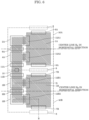
- Festkörperbildgebungsvorrichtung, umfassend eine Vielzahl von Pixeln, die in einer Matrix auf einem Halbleitersubstrat angeordnet sind,
wobei jedes der Vielzahl von Pixeln (50A) umfasst:einen photoelektrischen Wandler (1A), der dazu konfiguriert ist, Licht von einem Objekt zu empfangen und das Licht in eine Ladung umzuwandeln;einen Überlauf (8) der dazu konfiguriert ist, die Ladung des photoelektrischen Wandlers (1A) zu entladen;zwei Belichtungscontroller (6A), die dazu konfiguriert sind, zwischen der Akkumulation der Ladung in den photoelektrischen Wandler (1A) und der Entladung der Ladung aus dem photoelektrischen Wandler (1A) umzuschalten, wobei jeder der Belichtungscontroller (6A) ein Gate aufweist, an das ein Treiberimpulssignal (ODG1) angelegt wird, um zu steuern, dass eine Signalladung, die in dem photoelektrischen Wandler (1A) generiert wird, entweder an den Überlauf (8) über die Belichtungscontroller (6A) entladen wird und nicht in dem photoelektrischen Wandler (1A) akkumuliert wird, oder nicht an den Überlauf (8) entladen und in dem photoelektrischen Wandler (1A) akkumuliert wird;zwei Ladungsakkumulatoren (2A, 4A), die jeweils dazu konfiguriert sind, die Signalladung, die in dem photoelektrischen Wandler (1A) akkumuliert ist, zu halten;zwei Lesevorrichtungen (12A1, 12A2), die dazu konfiguriert sind, jeweils die Signalladung aus dem photoelektrischen Wandler (1A) in die beiden Ladungsakkumulatoren (2A, 4A) zu lesen und zwei Signale mit unterschiedlichen Belichtungsperioden zu erzielen;einen Übertragungscontroller (9A), der eine Übertragungssteuerung vornimmt, die das Steuern umfasst, ob die Ladung, die in einem der beiden Ladungsakkumulatoren (2A, 4A) akkumuliert ist, übertragen wird oder daran gehindert wird, auf einen anderen der beiden Ladungsakkumulatoren übertragen zu werden, undwobeider Übertragungscontroller (9A) zwischen den beiden Ladungsakkumulatoren (2a, 4A) angeordnet ist,jeder der beiden Belichtungscontroller (6A) und der beiden Lesevorrichtungen (12A1, 12A2) eine Gate-Elektrode aufweist, die auf dem Halbleitersubstrat gebildet ist, undin einer Draufsicht des Halbleitersubstrats eine Gate-Elektrode einer der beiden Lesevorrichtungen (12A1, 12A2) und eine Gate-Elektrode der anderen der beiden Lesevorrichtungen (12A1, 12A2) im Verhältnis zu einer Mittellinie (HA), die durch die Mitte einer Lichtempfangsregion des photoelektrischen Wandlers (1A) geht, axialsymmetrisch angeordnet sind und auf einer gleichen Seite einer äußeren Kante einer Lichtempfangsregion der photoelektrischen Wandler (1A) angeordnet sind, und die beiden Gate-Elektroden der Belichtungscontroller (6A) im Verhältnis zu der Mittellinie (HA) axialsymmetrisch angeordnet sind und auf zwei Seiten der äußern Kante der Lichtempfangsregion des photoelektrischen Wandlers (1A), die zu der gleichen Seite der äußeren Kante der Lichtempfangsregion des photoelektrischen Wandlers (1A) orthogonal sind, angeordnet sind. - Festkörperbildgebungsvorrichtung nach Anspruch 1,wobei der Übertragungscontroller (9A) zwischen den beiden Ladungsakkumulatoren (2A, 4A) in einer senkrechten Richtung angeordnet ist, unddie beiden Lesevorrichtungen (12A1, 12A2) jeweils zwischen dem photoelektrischen Wandler (1A) und den beiden Ladungsakkumulatoren (2A, 4A) in einer horizontalen Richtung angeordnet sind.
- Festkörperbildgebungsvorrichtung nach Anspruch 1 oder 2, wobei der Übertragungscontroller (9A) eine Gate-Elektrode aufweist, die auf ein gemeinsames Referenzpotential eingestellt ist.
- Festkörperbildgebungsvorrichtung nach Anspruch 1, wobei jedes der Vielzahl von Pixeln (50A, 50B) ferner umfasst
eine Lichtschutzfolie (20A, 20B), die mindestens einen Abschnitt einer Gate-Elektrode jedes der beiden Ladungsakkumulatoren (2A, 4A, 3B, 5B) vor Licht schützt und vermeidet, dass eine Gate-Elektrode des Belichtungscontrollers (6A, 7B) vor Licht geschützt wird. - Festkörperbildgebungsvorrichtung nach Anspruch 4, ferner umfassend
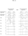
einen Treibercontroller, der das Ansteuern eines Treiberimpulssignals steuert, das an eine Gate-Elektrode jedes der Belichtungscontroller (6A, 7B) und an eine Gate-Elektrode jeder der beiden Lesevorrichtungen (12A1, 12A2, 12B1, 12B2) angelegt wird. - Festkörperbildgebungsvorrichtung nach Anspruch 5, ferner umfassendeine Vielzahl von Belichtungssteuerungs-Gate-Leitungen, die für jede Pixelreihe oder jede Pixelspalte bereitgestellt werden und über die das Treiberimpulssignal an die Gate-Elektrode des Belichtungscontrollers (6A, 7B) übertragen wird,wobei die Vielzahl von Belichtungssteuerungs-Gate-Leitungen parallel zu einer kurzen Seite einer Bildgebungsregion auf dem Halbleitersubstrat angeordnet ist, wobei die Bildgebungsregion eine Region ist, in der die Vielzahl von Pixeln angeordnet ist.
- Festkörperbildgebungsvorrichtung nach Anspruch 5 oder 6, ferner umfassendeine Lese-Gate-Leitung, über die das Treiberimpulssignal an die Gate-Elektrode jeder der beiden Lesevorrichtungen (12A1, 12A2) übertragen wird,wobei eine Gesamtanzahl des Umschaltens der Lese-Gate-Leitung auf einen hohen Pegel bei einer Vielzahl der Lese-Gate-Leitungen unterschiedlich ist.
- Festkörperbildgebungsvorrichtung nach einem der Ansprüche 5 bis 7, ferner umfassendeine Belichtungssteuerungs-Gate-Leitung, über die das Treiberimpulssignal von dem Treibercontroller an die Gate-Elektrode jedes der Belichtungscontroller (6A, 7B) übertragen wird,wobei eine Gesamtanzahl des Umschaltens der Belichtungssteuerungs-Gate-Leitung auf einen niedrigen Pegel bei einer Vielzahl der Belichtungssteuerungs-Gate-Leitungen unterschiedlich ist.
- Festkörperbildgebungsvorrichtung nach einem der Ansprüche 5 bis 8, wobei dem Treiberimpulssignal eine Gleichstrom- (DC) Vorspannung überlagert wird.
- Festkörperbildgebungsvorrichtung nach einem der Ansprüche 1 bis 9,wobei die Vielzahl von Pixeln mindestens ein erstes Pixel (50A) und ein zweites Pixel (50B) umfasst, die Infrarotlicht empfangen, unddas erste Pixel und das zweite Pixel gemeinsam eine schwebende Diffusion (10) nutzen, welche die Ladung der beiden Ladungsakkumulatoren (2A, 4A, 3B, 5B) in eine Spannung umwandelt.
- Festkörperbildgebungsvorrichtung nach Anspruch 10,wobei ein Treiberimpulssignal (VG1) an einen Ladungsakkumulator (2A) angelegt wird, der von den beiden Ladungsakkumulatoren (2A, 4A), die in dem ersten Pixel (50A) enthalten sind, weiter von der schwebenden Diffusion (10) entfernt angeordnet ist, und ein Treiberimpulssignal (VG4) an einen Ladungsakkumulator (5B) angelegt wird, der von den beiden Ladungsakkumulatoren (3B, 5B), die in dem zweiten Pixel (50B) enthalten sind, weiter von der schwebenden Diffusion (10) entfernt angeordnet ist,und wobei die Treiberimpulssignale (VG1, VG4) das gleiche Verhalten aufweisen.
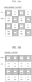
- Festkörperbildgebungsvorrichtung nach Anspruch 10 oder 11,wobei die Vielzahl von Pixeln eine Vielzahl von ersten Pixeln und eine Vielzahl von zweiten Pixeln umfasst, undin einer Draufsicht des Halbleitersubstrats die ersten Pixel und die zweiten Pixel in einem Schachbrettmuster angeordnet sind, unddie schwebende Diffusion in einem Schachbrettmuster in der Draufsicht angeordnet ist.
- Festkörperbildgebungsvorrichtung nach Anspruch 10 oder 11,wobei die Vielzahl von Pixeln eine Vielzahl von ersten Pixeln und eine Vielzahl von zweiten Pixeln umfasst, undin einer Draufsicht des Halbleitersubstrats die ersten Pixel und die zweiten Pixel in einem Streifenmuster angeordnet sind, unddie schwebende Diffusion in einem Streifenmuster in der Draufsicht angeordnet ist.
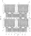
- Festkörperbildgebungsvorrichtung nach Anspruch 10,wobei die Vielzahl von Pixeln ein drittes Pixel, ein viertes Pixel, ein fünftes Pixel und ein sechstes Pixel umfassen, die zweidimensional angeordnet sind,wobei das dritte Pixel umfasst:den photoelektrischen Wandler, dessen Anzahl eins ist;die beiden Belichtungscontroller; undvier Lesevorrichtungen, welche die Ladung aus dem photoelektrischen Wandler lesen, undjedes von dem vierten Pixel, dem fünften Pixel und dem sechsten Pixel umfasst:den photoelektrischen Wandler, dessen Anzahl eins ist;die beiden Belichtungscontroller; unddie beiden Lesevorrichtungen.
- Festkörperbildgebungsvorrichtung nach Anspruch 14, wobei jedes von dem dritten Pixel, dem fünften Pixel und dem sechsten Pixel ferner umfasstdie beiden Ladungsakkumulatoren, unddas vierte Pixel umfasstdie beiden Ladungsakkumulatoren, welche die Ladung, die aus dem photoelektrischen Wandler des dritten Pixels durch zwei Lesevorrichtungen von den vier Lesevorrichtungen des dritten Pixels gelesen werden, und die Ladung, die aus dem photoelektrischen Wandler des vierten Pixels durch die beiden Lesevorrichtungen des vierten Pixels gelesen werden, kumulieren.
- Festkörperbildgebungsvorrichtung nach Anspruch 14, ferner umfassend
einen Treibercontroller, das die Ansteuerung eines Treiberimpulssignals steuert, das an die Gate-Elektrode jedes der beiden Belichtungscontroller, der zwei Lesevorrichtungen und der vier Lesevorrichtungen angelegt wird:
einen Bildansteuerungsmodus, in dem ein Farbbild unter Verwendung der vierten bis sechsten Pixel erzielt wird; und einen Modus zum Ansteuern einer Abstandsmessung, bei dem das Licht von dem Objekt basierend auf einem gepulsten Strahl, der an das Objekt emittiert wird, unter Verwendung des photoelektrischen Wandlers des dritten Pixels in eine Ladung umgewandelt wird, und ein Signal zur Abstandsberechnung unter Verwendung der Ladungsakkumulatoren des dritten Pixels und des vierten Pixels erzielt wird. - Festkörperbildgebungsvorrichtung nach einem der Ansprüche 15 bis 16, wobei die dritten bis sechsten Pixel eine Pixelgruppe bilden, die vier Pixel hoch mal vier Pixel breit ist, und in der Draufsicht das dritte Pixel in einem Schachbrettmuster in der Pixelgruppe angeordnet ist.
Applications Claiming Priority (2)
| Application Number | Priority Date | Filing Date | Title |
|---|---|---|---|
| JP2015154552 | 2015-08-04 | ||
| PCT/JP2016/003493 WO2017022218A1 (ja) | 2015-08-04 | 2016-07-28 | 固体撮像装置 |
Publications (3)
| Publication Number | Publication Date |
|---|---|
| EP3334152A1 EP3334152A1 (de) | 2018-06-13 |
| EP3334152A4 EP3334152A4 (de) | 2018-08-22 |
| EP3334152B1 true EP3334152B1 (de) | 2023-10-11 |
Family
ID=57942686
Family Applications (1)
| Application Number | Title | Priority Date | Filing Date |
|---|---|---|---|
| EP16832501.7A Active EP3334152B1 (de) | 2015-08-04 | 2016-07-28 | Festkörperbildgebungsvorrichtung |
Country Status (5)
| Country | Link |
|---|---|
| US (1) | US10666875B2 (de) |
| EP (1) | EP3334152B1 (de) |
| JP (1) | JP6738334B2 (de) |
| CN (1) | CN107925733B (de) |
| WO (1) | WO2017022218A1 (de) |
Families Citing this family (10)
| Publication number | Priority date | Publication date | Assignee | Title |
|---|---|---|---|---|
| CN108389870A (zh) | 2017-02-03 | 2018-08-10 | 松下知识产权经营株式会社 | 摄像装置 |
| JP6653482B2 (ja) * | 2017-04-06 | 2020-02-26 | パナソニックIpマネジメント株式会社 | 撮像装置、およびそれに用いられる固体撮像装置 |
| DE112018006100T5 (de) * | 2017-12-26 | 2020-10-29 | Robert Bosch Gmbh | Einzelchip-rgb-d-kamera |
| KR102488321B1 (ko) * | 2017-12-29 | 2023-01-13 | 삼성전자주식회사 | 3차원 이미지 센서의 픽셀 어레이 및 3차원 이미지 센서의 구동 방법 |
| US11092678B2 (en) * | 2018-06-21 | 2021-08-17 | Analog Devices, Inc. | Measuring and removing the corruption of time-of-flight depth images due to internal scattering |
| KR102615195B1 (ko) * | 2018-07-19 | 2023-12-18 | 삼성전자주식회사 | ToF 기반의 3D 이미지 센서 및 그 이미지 센서를 구비한 전자 장치 |
| CN112888958A (zh) * | 2018-10-16 | 2021-06-01 | 布鲁克曼科技株式会社 | 测距装置、摄像头以及测距装置的驱动调整方法 |
| WO2020195046A1 (ja) * | 2019-03-27 | 2020-10-01 | パナソニックIpマネジメント株式会社 | 固体撮像装置 |
| CN110346780A (zh) * | 2019-07-31 | 2019-10-18 | 炬佑智能科技(苏州)有限公司 | 飞行时间传感相机及其局部检测精度调整方法 |
| CN110456380B (zh) * | 2019-07-31 | 2021-12-28 | 炬佑智能科技(苏州)有限公司 | 飞行时间传感相机及其深度检测方法 |
Citations (2)
| Publication number | Priority date | Publication date | Assignee | Title |
|---|---|---|---|---|
| WO2007119626A1 (ja) * | 2006-03-31 | 2007-10-25 | National University Corporation Shizuoka University | 半導体測距素子及び固体撮像装置 |
| US20120248290A1 (en) * | 2011-03-31 | 2012-10-04 | Honda Motor Co., Ltd. | Solid-state image sensing device |
Family Cites Families (9)
| Publication number | Priority date | Publication date | Assignee | Title |
|---|---|---|---|---|
| JP4235729B2 (ja) | 2003-02-03 | 2009-03-11 | 国立大学法人静岡大学 | 距離画像センサ |
| JP4524609B2 (ja) * | 2004-10-29 | 2010-08-18 | ソニー株式会社 | 固体撮像素子、固体撮像素子の駆動方法および撮像装置 |
| TWI433307B (zh) * | 2008-10-22 | 2014-04-01 | Sony Corp | 固態影像感測器、其驅動方法、成像裝置及電子器件 |
| JP2010161183A (ja) * | 2009-01-07 | 2010-07-22 | Panasonic Corp | 固体撮像装置 |
| JP5404112B2 (ja) | 2009-03-12 | 2014-01-29 | キヤノン株式会社 | 固体撮像素子、その駆動方法及び撮像システム |
| US8179463B1 (en) * | 2009-05-19 | 2012-05-15 | On Semiconductor Trading Ltd. | Image sensor with shared node |
| WO2014002415A1 (ja) * | 2012-06-28 | 2014-01-03 | パナソニック株式会社 | 撮像装置 |
| WO2015011869A1 (ja) * | 2013-07-23 | 2015-01-29 | パナソニックIpマネジメント株式会社 | 撮像装置及びその駆動方法 |
| WO2015025497A1 (ja) * | 2013-08-23 | 2015-02-26 | パナソニックIpマネジメント株式会社 | 測距システム及び信号発生装置 |
-
2016
- 2016-07-28 WO PCT/JP2016/003493 patent/WO2017022218A1/ja active Application Filing
- 2016-07-28 EP EP16832501.7A patent/EP3334152B1/de active Active
- 2016-07-28 CN CN201680045328.2A patent/CN107925733B/zh active Active
- 2016-07-28 JP JP2017532369A patent/JP6738334B2/ja active Active
-
2018
- 2018-01-29 US US15/882,316 patent/US10666875B2/en active Active
Patent Citations (4)
| Publication number | Priority date | Publication date | Assignee | Title |
|---|---|---|---|---|
| WO2007119626A1 (ja) * | 2006-03-31 | 2007-10-25 | National University Corporation Shizuoka University | 半導体測距素子及び固体撮像装置 |
| US20090114919A1 (en) * | 2006-03-31 | 2009-05-07 | National University Corporation Shizuoka Univ. | Semiconductor range-finding element and solid-state imaging device |
| US20120248290A1 (en) * | 2011-03-31 | 2012-10-04 | Honda Motor Co., Ltd. | Solid-state image sensing device |
| JP2012217060A (ja) * | 2011-03-31 | 2012-11-08 | Honda Motor Co Ltd | 固体撮像装置 |
Also Published As
| Publication number | Publication date |
|---|---|
| US10666875B2 (en) | 2020-05-26 |
| JPWO2017022218A1 (ja) | 2018-05-24 |
| US20180167562A1 (en) | 2018-06-14 |
| JP6738334B2 (ja) | 2020-08-12 |
| EP3334152A4 (de) | 2018-08-22 |
| EP3334152A1 (de) | 2018-06-13 |
| WO2017022218A1 (ja) | 2017-02-09 |
| CN107925733B (zh) | 2020-09-18 |
| CN107925733A (zh) | 2018-04-17 |
Similar Documents
| Publication | Publication Date | Title |
|---|---|---|
| EP3333893B1 (de) | Festkörperbildgebungsvorrichtung | |
| EP3334152B1 (de) | Festkörperbildgebungsvorrichtung | |
| US10838066B2 (en) | Solid-state imaging device, distance measurement device, and distance measurement method | |
| JP6145826B2 (ja) | 撮像装置及びその駆動方法 | |
| EP2803184B1 (de) | Verfahren zum betreiben eines flugzeitpixels | |
| US8686367B2 (en) | Circuit configuration and method for time of flight sensor | |
| CN107852470B (zh) | 固体摄像装置的驱动方法 | |
| US10491842B2 (en) | Imaging device, a solid-state imaging device for use in the imaging device | |
| US11399148B2 (en) | Solid-state imaging device and imaging apparatus including same | |
| JP2011128024A (ja) | 3次元撮像装置 | |
| US10048380B2 (en) | Distance-measuring imaging device and solid state imaging element | |
| JPWO2016133053A1 (ja) | 距離画像計測装置 | |
| US11194025B2 (en) | Solid-state imaging device and imaging apparatus including same | |
| US20220357445A1 (en) | Distance image measuring device |
Legal Events
| Date | Code | Title | Description |
|---|---|---|---|
| STAA | Information on the status of an ep patent application or granted ep patent |
Free format text: STATUS: THE INTERNATIONAL PUBLICATION HAS BEEN MADE |
|
| PUAI | Public reference made under article 153(3) epc to a published international application that has entered the european phase |
Free format text: ORIGINAL CODE: 0009012 |
|
| STAA | Information on the status of an ep patent application or granted ep patent |
Free format text: STATUS: REQUEST FOR EXAMINATION WAS MADE |
|
| 17P | Request for examination filed |
Effective date: 20180125 |
|
| AK | Designated contracting states |
Kind code of ref document: A1 Designated state(s): AL AT BE BG CH CY CZ DE DK EE ES FI FR GB GR HR HU IE IS IT LI LT LU LV MC MK MT NL NO PL PT RO RS SE SI SK SM TR |
|
| AX | Request for extension of the european patent |
Extension state: BA ME |
|
| A4 | Supplementary search report drawn up and despatched |
Effective date: 20180720 |
|
| RIC1 | Information provided on ipc code assigned before grant |
Ipc: G01S 17/89 20060101ALI20180716BHEP Ipc: H04N 5/369 20110101ALI20180716BHEP Ipc: H01L 27/146 20060101ALI20180716BHEP Ipc: G01S 7/486 20060101AFI20180716BHEP |
|
| DAV | Request for validation of the european patent (deleted) | ||
| DAX | Request for extension of the european patent (deleted) | ||
| STAA | Information on the status of an ep patent application or granted ep patent |
Free format text: STATUS: EXAMINATION IS IN PROGRESS |
|
| 17Q | First examination report despatched |
Effective date: 20200511 |
|
| RAP1 | Party data changed (applicant data changed or rights of an application transferred) |
Owner name: PANASONIC SEMICONDUCTOR SOLUTIONS CO., LTD. |
|
| STAA | Information on the status of an ep patent application or granted ep patent |
Free format text: STATUS: EXAMINATION IS IN PROGRESS |
|
| RAP3 | Party data changed (applicant data changed or rights of an application transferred) |
Owner name: NUVOTON TECHNOLOGY CORPORATION JAPAN |
|
| RAP3 | Party data changed (applicant data changed or rights of an application transferred) |
Owner name: NUVOTON TECHNOLOGY CORPORATION JAPAN |
|
| REG | Reference to a national code |
Ref country code: DE Ref legal event code: R079 Ref document number: 602016083415 Country of ref document: DE Free format text: PREVIOUS MAIN CLASS: H04N0005369000 Ipc: H04N0025700000 Ref legal event code: R079 Ipc: H04N0025700000 |
|
| RIC1 | Information provided on ipc code assigned before grant |
Ipc: G01S 17/894 20200101ALI20230427BHEP Ipc: G01S 7/4863 20200101ALI20230427BHEP Ipc: G01S 7/481 20060101ALI20230427BHEP Ipc: H01L 27/146 20060101ALI20230427BHEP Ipc: H04N 25/70 20230101AFI20230427BHEP |
|
| GRAP | Despatch of communication of intention to grant a patent |
Free format text: ORIGINAL CODE: EPIDOSNIGR1 |
|
| STAA | Information on the status of an ep patent application or granted ep patent |
Free format text: STATUS: GRANT OF PATENT IS INTENDED |
|
| INTG | Intention to grant announced |
Effective date: 20230615 |
|
| GRAS | Grant fee paid |
Free format text: ORIGINAL CODE: EPIDOSNIGR3 |
|
| GRAA | (expected) grant |
Free format text: ORIGINAL CODE: 0009210 |
|
| STAA | Information on the status of an ep patent application or granted ep patent |
Free format text: STATUS: THE PATENT HAS BEEN GRANTED |
|
| AK | Designated contracting states |
Kind code of ref document: B1 Designated state(s): AL AT BE BG CH CY CZ DE DK EE ES FI FR GB GR HR HU IE IS IT LI LT LU LV MC MK MT NL NO PL PT RO RS SE SI SK SM TR |
|
| REG | Reference to a national code |
Ref country code: GB Ref legal event code: FG4D |
|
| REG | Reference to a national code |
Ref country code: CH Ref legal event code: EP |
|
| REG | Reference to a national code |
Ref country code: DE Ref legal event code: R096 Ref document number: 602016083415 Country of ref document: DE |
|
| P01 | Opt-out of the competence of the unified patent court (upc) registered |
Effective date: 20231004 |
|
| REG | Reference to a national code |
Ref country code: IE Ref legal event code: FG4D |
|
| REG | Reference to a national code |
Ref country code: LT Ref legal event code: MG9D |
|
| REG | Reference to a national code |
Ref country code: NL Ref legal event code: MP Effective date: 20231011 |
|
| REG | Reference to a national code |
Ref country code: AT Ref legal event code: MK05 Ref document number: 1621417 Country of ref document: AT Kind code of ref document: T Effective date: 20231011 |
|
| P03 | Opt-out of the competence of the unified patent court (upc) deleted | ||
| PG25 | Lapsed in a contracting state [announced via postgrant information from national office to epo] |
Ref country code: NL Free format text: LAPSE BECAUSE OF FAILURE TO SUBMIT A TRANSLATION OF THE DESCRIPTION OR TO PAY THE FEE WITHIN THE PRESCRIBED TIME-LIMIT Effective date: 20231011 |
|
| PG25 | Lapsed in a contracting state [announced via postgrant information from national office to epo] |
Ref country code: GR Free format text: LAPSE BECAUSE OF FAILURE TO SUBMIT A TRANSLATION OF THE DESCRIPTION OR TO PAY THE FEE WITHIN THE PRESCRIBED TIME-LIMIT Effective date: 20240112 |
|
| PG25 | Lapsed in a contracting state [announced via postgrant information from national office to epo] |
Ref country code: IS Free format text: LAPSE BECAUSE OF FAILURE TO SUBMIT A TRANSLATION OF THE DESCRIPTION OR TO PAY THE FEE WITHIN THE PRESCRIBED TIME-LIMIT Effective date: 20240211 |
|
| PG25 | Lapsed in a contracting state [announced via postgrant information from national office to epo] |
Ref country code: LT Free format text: LAPSE BECAUSE OF FAILURE TO SUBMIT A TRANSLATION OF THE DESCRIPTION OR TO PAY THE FEE WITHIN THE PRESCRIBED TIME-LIMIT Effective date: 20231011 |
|
| PG25 | Lapsed in a contracting state [announced via postgrant information from national office to epo] |
Ref country code: AT Free format text: LAPSE BECAUSE OF FAILURE TO SUBMIT A TRANSLATION OF THE DESCRIPTION OR TO PAY THE FEE WITHIN THE PRESCRIBED TIME-LIMIT Effective date: 20231011 |
|
| PG25 | Lapsed in a contracting state [announced via postgrant information from national office to epo] |
Ref country code: ES Free format text: LAPSE BECAUSE OF FAILURE TO SUBMIT A TRANSLATION OF THE DESCRIPTION OR TO PAY THE FEE WITHIN THE PRESCRIBED TIME-LIMIT Effective date: 20231011 |
|
| PG25 | Lapsed in a contracting state [announced via postgrant information from national office to epo] |
Ref country code: LT Free format text: LAPSE BECAUSE OF FAILURE TO SUBMIT A TRANSLATION OF THE DESCRIPTION OR TO PAY THE FEE WITHIN THE PRESCRIBED TIME-LIMIT Effective date: 20231011 Ref country code: IS Free format text: LAPSE BECAUSE OF FAILURE TO SUBMIT A TRANSLATION OF THE DESCRIPTION OR TO PAY THE FEE WITHIN THE PRESCRIBED TIME-LIMIT Effective date: 20240211 Ref country code: GR Free format text: LAPSE BECAUSE OF FAILURE TO SUBMIT A TRANSLATION OF THE DESCRIPTION OR TO PAY THE FEE WITHIN THE PRESCRIBED TIME-LIMIT Effective date: 20240112 Ref country code: ES Free format text: LAPSE BECAUSE OF FAILURE TO SUBMIT A TRANSLATION OF THE DESCRIPTION OR TO PAY THE FEE WITHIN THE PRESCRIBED TIME-LIMIT Effective date: 20231011 Ref country code: BG Free format text: LAPSE BECAUSE OF FAILURE TO SUBMIT A TRANSLATION OF THE DESCRIPTION OR TO PAY THE FEE WITHIN THE PRESCRIBED TIME-LIMIT Effective date: 20240111 Ref country code: AT Free format text: LAPSE BECAUSE OF FAILURE TO SUBMIT A TRANSLATION OF THE DESCRIPTION OR TO PAY THE FEE WITHIN THE PRESCRIBED TIME-LIMIT Effective date: 20231011 Ref country code: PT Free format text: LAPSE BECAUSE OF FAILURE TO SUBMIT A TRANSLATION OF THE DESCRIPTION OR TO PAY THE FEE WITHIN THE PRESCRIBED TIME-LIMIT Effective date: 20240212 |