EP3334151A1 - Solid state image pickup device driving method - Google Patents
Solid state image pickup device driving method Download PDFInfo
- Publication number
- EP3334151A1 EP3334151A1 EP16832502.5A EP16832502A EP3334151A1 EP 3334151 A1 EP3334151 A1 EP 3334151A1 EP 16832502 A EP16832502 A EP 16832502A EP 3334151 A1 EP3334151 A1 EP 3334151A1
- Authority
- EP
- European Patent Office
- Prior art keywords
- exposure
- reader
- charge
- imaging device
- solid
- Prior art date
- Legal status (The legal status is an assumption and is not a legal conclusion. Google has not performed a legal analysis and makes no representation as to the accuracy of the status listed.)
- Granted
Links
- 238000000034 method Methods 0.000 title claims abstract description 49
- 239000007787 solid Substances 0.000 title 1
- 238000003384 imaging method Methods 0.000 claims abstract description 94
- 238000007599 discharging Methods 0.000 claims abstract description 4
- 238000005259 measurement Methods 0.000 claims description 199
- 238000006243 chemical reaction Methods 0.000 claims description 93
- 239000000758 substrate Substances 0.000 claims description 15
- 238000009792 diffusion process Methods 0.000 claims description 11
- 239000004065 semiconductor Substances 0.000 claims description 9
- 230000003321 amplification Effects 0.000 claims description 8
- 238000003199 nucleic acid amplification method Methods 0.000 claims description 8
- 238000007667 floating Methods 0.000 claims description 7
- 230000035508 accumulation Effects 0.000 description 70
- 238000009825 accumulation Methods 0.000 description 70
- 230000007704 transition Effects 0.000 description 32
- 230000001678 irradiating effect Effects 0.000 description 27
- 101100298888 Arabidopsis thaliana PAD2 gene Proteins 0.000 description 14
- 101100030928 Arabidopsis thaliana PAF1 gene Proteins 0.000 description 14
- 101100465385 Arabidopsis thaliana PAF2 gene Proteins 0.000 description 14
- 101100398338 Enterococcus faecalis (strain ATCC 700802 / V583) prs2 gene Proteins 0.000 description 14
- 101100510342 Listeria ivanovii prs gene Proteins 0.000 description 14
- 101100137870 Saccharomyces cerevisiae (strain ATCC 204508 / S288c) PRE10 gene Proteins 0.000 description 14
- 230000003287 optical effect Effects 0.000 description 14
- 101150077839 pac1 gene Proteins 0.000 description 14
- 101150086435 prs1 gene Proteins 0.000 description 14
- 230000035945 sensitivity Effects 0.000 description 13
- 238000012546 transfer Methods 0.000 description 11
- 238000004364 calculation method Methods 0.000 description 10
- 230000000694 effects Effects 0.000 description 8
- 238000009826 distribution Methods 0.000 description 7
- 230000008859 change Effects 0.000 description 6
- 230000014509 gene expression Effects 0.000 description 6
- 230000006872 improvement Effects 0.000 description 6
- 239000012535 impurity Substances 0.000 description 5
- 230000002123 temporal effect Effects 0.000 description 5
- 101100288173 Enterococcus faecalis (strain ATCC 700802 / V583) prs1 gene Proteins 0.000 description 4
- 101100465401 Saccharomyces cerevisiae (strain ATCC 204508 / S288c) SCL1 gene Proteins 0.000 description 4
- 238000013459 approach Methods 0.000 description 4
- 230000003071 parasitic effect Effects 0.000 description 4
- 101150016674 prs2 gene Proteins 0.000 description 4
- 238000010586 diagram Methods 0.000 description 3
- 230000006870 function Effects 0.000 description 3
- 238000004519 manufacturing process Methods 0.000 description 3
- 230000008569 process Effects 0.000 description 3
- 230000000630 rising effect Effects 0.000 description 3
- 238000002366 time-of-flight method Methods 0.000 description 3
- 238000007796 conventional method Methods 0.000 description 2
- 239000010949 copper Substances 0.000 description 2
- 230000003111 delayed effect Effects 0.000 description 2
- 229910052751 metal Inorganic materials 0.000 description 2
- 239000002184 metal Substances 0.000 description 2
- 230000009467 reduction Effects 0.000 description 2
- 238000003860 storage Methods 0.000 description 2
- RYGMFSIKBFXOCR-UHFFFAOYSA-N Copper Chemical compound [Cu] RYGMFSIKBFXOCR-UHFFFAOYSA-N 0.000 description 1
- 229910052782 aluminium Inorganic materials 0.000 description 1
- XAGFODPZIPBFFR-UHFFFAOYSA-N aluminium Chemical compound [Al] XAGFODPZIPBFFR-UHFFFAOYSA-N 0.000 description 1
- 230000015556 catabolic process Effects 0.000 description 1
- 230000000295 complement effect Effects 0.000 description 1
- 229910052802 copper Inorganic materials 0.000 description 1
- 230000008878 coupling Effects 0.000 description 1
- 238000010168 coupling process Methods 0.000 description 1
- 238000005859 coupling reaction Methods 0.000 description 1
- 230000003247 decreasing effect Effects 0.000 description 1
- 238000006731 degradation reaction Methods 0.000 description 1
- 238000001514 detection method Methods 0.000 description 1
- 238000005516 engineering process Methods 0.000 description 1
- 229910000765 intermetallic Inorganic materials 0.000 description 1
- 238000002955 isolation Methods 0.000 description 1
- 239000000463 material Substances 0.000 description 1
- 238000012986 modification Methods 0.000 description 1
- 230000004048 modification Effects 0.000 description 1
- 238000005036 potential barrier Methods 0.000 description 1
- 238000005070 sampling Methods 0.000 description 1
- WFKWXMTUELFFGS-UHFFFAOYSA-N tungsten Chemical compound [W] WFKWXMTUELFFGS-UHFFFAOYSA-N 0.000 description 1
- 229910052721 tungsten Inorganic materials 0.000 description 1
- 239000010937 tungsten Substances 0.000 description 1
Images


Classifications
-
- G—PHYSICS
- G01—MEASURING; TESTING
- G01S—RADIO DIRECTION-FINDING; RADIO NAVIGATION; DETERMINING DISTANCE OR VELOCITY BY USE OF RADIO WAVES; LOCATING OR PRESENCE-DETECTING BY USE OF THE REFLECTION OR RERADIATION OF RADIO WAVES; ANALOGOUS ARRANGEMENTS USING OTHER WAVES
- G01S7/00—Details of systems according to groups G01S13/00, G01S15/00, G01S17/00
- G01S7/48—Details of systems according to groups G01S13/00, G01S15/00, G01S17/00 of systems according to group G01S17/00
- G01S7/483—Details of pulse systems
- G01S7/486—Receivers
- G01S7/4868—Controlling received signal intensity or exposure of sensor
-
- G—PHYSICS
- G01—MEASURING; TESTING
- G01S—RADIO DIRECTION-FINDING; RADIO NAVIGATION; DETERMINING DISTANCE OR VELOCITY BY USE OF RADIO WAVES; LOCATING OR PRESENCE-DETECTING BY USE OF THE REFLECTION OR RERADIATION OF RADIO WAVES; ANALOGOUS ARRANGEMENTS USING OTHER WAVES
- G01S17/00—Systems using the reflection or reradiation of electromagnetic waves other than radio waves, e.g. lidar systems
- G01S17/02—Systems using the reflection of electromagnetic waves other than radio waves
- G01S17/06—Systems determining position data of a target
- G01S17/08—Systems determining position data of a target for measuring distance only
- G01S17/10—Systems determining position data of a target for measuring distance only using transmission of interrupted, pulse-modulated waves
-
- G—PHYSICS
- G01—MEASURING; TESTING
- G01S—RADIO DIRECTION-FINDING; RADIO NAVIGATION; DETERMINING DISTANCE OR VELOCITY BY USE OF RADIO WAVES; LOCATING OR PRESENCE-DETECTING BY USE OF THE REFLECTION OR RERADIATION OF RADIO WAVES; ANALOGOUS ARRANGEMENTS USING OTHER WAVES
- G01S17/00—Systems using the reflection or reradiation of electromagnetic waves other than radio waves, e.g. lidar systems
- G01S17/88—Lidar systems specially adapted for specific applications
- G01S17/89—Lidar systems specially adapted for specific applications for mapping or imaging
- G01S17/894—3D imaging with simultaneous measurement of time-of-flight at a 2D array of receiver pixels, e.g. time-of-flight cameras or flash lidar
-
- G—PHYSICS
- G01—MEASURING; TESTING
- G01S—RADIO DIRECTION-FINDING; RADIO NAVIGATION; DETERMINING DISTANCE OR VELOCITY BY USE OF RADIO WAVES; LOCATING OR PRESENCE-DETECTING BY USE OF THE REFLECTION OR RERADIATION OF RADIO WAVES; ANALOGOUS ARRANGEMENTS USING OTHER WAVES
- G01S7/00—Details of systems according to groups G01S13/00, G01S15/00, G01S17/00
- G01S7/48—Details of systems according to groups G01S13/00, G01S15/00, G01S17/00 of systems according to group G01S17/00
- G01S7/483—Details of pulse systems
- G01S7/486—Receivers
- G01S7/4861—Circuits for detection, sampling, integration or read-out
- G01S7/4863—Detector arrays, e.g. charge-transfer gates
-
- G—PHYSICS
- G01—MEASURING; TESTING
- G01S—RADIO DIRECTION-FINDING; RADIO NAVIGATION; DETERMINING DISTANCE OR VELOCITY BY USE OF RADIO WAVES; LOCATING OR PRESENCE-DETECTING BY USE OF THE REFLECTION OR RERADIATION OF RADIO WAVES; ANALOGOUS ARRANGEMENTS USING OTHER WAVES
- G01S7/00—Details of systems according to groups G01S13/00, G01S15/00, G01S17/00
- G01S7/48—Details of systems according to groups G01S13/00, G01S15/00, G01S17/00 of systems according to group G01S17/00
- G01S7/483—Details of pulse systems
- G01S7/486—Receivers
- G01S7/4865—Time delay measurement, e.g. time-of-flight measurement, time of arrival measurement or determining the exact position of a peak
-
- H—ELECTRICITY
- H01—ELECTRIC ELEMENTS
- H01L—SEMICONDUCTOR DEVICES NOT COVERED BY CLASS H10
- H01L27/00—Devices consisting of a plurality of semiconductor or other solid-state components formed in or on a common substrate
- H01L27/14—Devices consisting of a plurality of semiconductor or other solid-state components formed in or on a common substrate including semiconductor components sensitive to infrared radiation, light, electromagnetic radiation of shorter wavelength or corpuscular radiation and specially adapted either for the conversion of the energy of such radiation into electrical energy or for the control of electrical energy by such radiation
- H01L27/144—Devices controlled by radiation
- H01L27/146—Imager structures
- H01L27/148—Charge coupled imagers
- H01L27/14806—Structural or functional details thereof
- H01L27/14812—Special geometry or disposition of pixel-elements, address lines or gate-electrodes
- H01L27/14818—Optical shielding
-
- H—ELECTRICITY
- H01—ELECTRIC ELEMENTS
- H01L—SEMICONDUCTOR DEVICES NOT COVERED BY CLASS H10
- H01L27/00—Devices consisting of a plurality of semiconductor or other solid-state components formed in or on a common substrate
- H01L27/14—Devices consisting of a plurality of semiconductor or other solid-state components formed in or on a common substrate including semiconductor components sensitive to infrared radiation, light, electromagnetic radiation of shorter wavelength or corpuscular radiation and specially adapted either for the conversion of the energy of such radiation into electrical energy or for the control of electrical energy by such radiation
- H01L27/144—Devices controlled by radiation
- H01L27/146—Imager structures
- H01L27/148—Charge coupled imagers
- H01L27/14831—Area CCD imagers
- H01L27/14856—Time-delay and integration
-
- H—ELECTRICITY
- H04—ELECTRIC COMMUNICATION TECHNIQUE
- H04N—PICTORIAL COMMUNICATION, e.g. TELEVISION
- H04N23/00—Cameras or camera modules comprising electronic image sensors; Control thereof
- H04N23/70—Circuitry for compensating brightness variation in the scene
- H04N23/71—Circuitry for evaluating the brightness variation
-
- H—ELECTRICITY
- H04—ELECTRIC COMMUNICATION TECHNIQUE
- H04N—PICTORIAL COMMUNICATION, e.g. TELEVISION
- H04N25/00—Circuitry of solid-state image sensors [SSIS]; Control thereof
- H04N25/50—Control of the SSIS exposure
- H04N25/53—Control of the integration time
-
- H—ELECTRICITY
- H04—ELECTRIC COMMUNICATION TECHNIQUE
- H04N—PICTORIAL COMMUNICATION, e.g. TELEVISION
- H04N25/00—Circuitry of solid-state image sensors [SSIS]; Control thereof
- H04N25/70—SSIS architectures; Circuits associated therewith
- H04N25/76—Addressed sensors, e.g. MOS or CMOS sensors
Definitions
- the present invention relates to methods for driving solid-state imaging devices to be used in imaging for distance measurement.
- TOF time of flight
- Patent Literature (PTL) 1 discloses a distance image sensor in which two different signal storage units store signals obtained by transfer of charge with different phases in synchronization with intermittent behavior of light from a light source, the distance to an object is determined using the distribution ratio of the stored signals, and furthermore, a third signal storage unit stores signals of background light only, and thus background light removal is performed to eliminate the impact of the background light.
- exposure periods T1 to T3 are set to have the same length as pulse width Tp where T1 is a first exposure period starting from time of a rising edge of irradiating light having pulse width Tp, T2 is a second exposure period starting from time of a falling edge of the irradiating light, and T3 is a third exposure period in which exposure is performed in a state where the irradiating light is OFF.
- the present invention has an object to provide a method for driving a solid-state imaging device which is small, has high distance measurement accuracy, and obtains a distance measurement signal that covers a wide distance measurement range.
- a method for driving a solid-state imaging device is a method for driving a solid-state imaging device which captures a distance measurement image for measuring a distance to an object irradiated with a pulsed beam having a predetermined pulse width and includes, on a semiconductor substrate, a unit pixel including: a photoelectric converter which receives reflected light from the object and converts the reflected light into charge; a charge discharger which discharges the charge of the photoelectric converter; an exposure resetter which switches timing for accumulating the charge in the photoelectric converter and timing for discharging the charge from the photoelectric converter to the charge discharger; n charge accumulators which accumulate the charge of the photoelectric converter where n is a natural number; and n readers which are provided between the photoelectric converter and the n charge accumulators and read the charge from the photoelectric converter to the n charge accumulators where n is a natural number.
- the method for driving the solid-state imaging device includes performing an exposure sequence including: an exposure start step of starting exposure of the photoelectric converter by placing the exposure resetter in a non-conducting state after a lapse of a predetermined period of time starting when the n readers are placed in a conducting state; and an exposure stop step of stopping the exposure of the photoelectric converter by placing the exposure resetter in the conducting state a predetermined period of time before placing the n readers in the non-conducting state after the exposure is started.
- a small solid-state imaging device can obtain a distance measurement signal that covers a wide distance measurement range with high distance measurement accuracy.
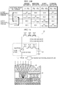
- FIG. 15A is a schematic configuration view of a conventional distance measurement pixel which obtains distance measurement information using three unit pixels.
- FIG. 15B is a timing chart for describing distance measurement driving of a conventional distance measurement device.
- FIG. 16 illustrates transitions of a pixel potential distribution at the time of distance measurement driving of the conventional distance measurement device.
- FIG. 15A structural elements of three unit pixels 70A, 70B, and 70C are illustrated, and three unit pixels 70A, 70B, and 70C form one distance measurement pixel 70.
- Unit pixel 70A includes one photoelectric conversion element 50A, read gate TG0, charge accumulation gate SG0, output gate OG0, and exposure reset gate PRS0.
- Unit pixel 70B includes one photoelectric conversion element 50B, a read gate TG1, charge accumulation gate SG1, output gate OG1, and exposure reset gate PRS1.
- Unit pixel 70C includes one photoelectric conversion element 50C, read gate TG2, charge accumulation gate SG2, output gate OG2, and exposure reset gate PRS2.
- distance measurement pixel 70 includes: floating diffusion (FD) 61 which is shared by three unit pixels 70A, 70B, and 70C; amplification transistor 63; reset transistor 64; and selection transistor 65.
- FD floating diffusion
- distance measurement pixel 70 having the abovementioned configuration, as illustrated in FIG. 15B , at the time of exposure of each photoelectric conversion element, the operation of starting the signal reading from the photoelectric conversion element to the charge accumulation gate and the operation of stopping the signal discharge from the photoelectric conversion element to drain VPRD are performed at the same time. Furthermore, the operation of stopping the signal reading from the photoelectric conversion element to the charge accumulation gate and the operation of starting the signal discharge from the photoelectric conversion element to drain VPRD are performed at the same time. Next, distance measurement driving of the conventional distance measurement device will be described.
- read gate TG0 of unit pixel 70A (S0 exposure pixel) is OFF, exposure reset gate PRS0 is ON, and signal charge of photoelectric conversion element 50A is discharged to drain VPRD (P1 in FIG. 16 : discharge).
- read gate TG0 is switched OFF again (VH to VL), and exposure reset gate PRS0 is switched ON (VL to VH); thus, the charge of photoelectric conversion element 50A is discharged to drain VPRD, resulting in completion of S0 exposure sequence at unit pixel 70A.
- read gate TG1 is switched ON (VL to VH), and exposure reset gate PRS1 is switched OFF (VH to VL); thus, the signal charge of photoelectric conversion element 50B is transferred to charge accumulation gate SG1 and accumulated therein.
- read gate TG1 is switched OFF again (VH to VL), and exposure reset gate PRS1 is switched ON (VL to VH); thus, the charge of photoelectric conversion element 50B is discharged to drain VPRD, resulting in completion of S1 exposure sequence at unit pixel 70B.
- unit pixel 70C (BG exposure pixel)
- read gate TG2 is OFF
- exposure reset gate PRS2 is ON
- signal charge of photoelectric conversion element 50C is discharged to drain VPRD.
- read gate TG2 is switched ON (VL to VH), and exposure reset gate PRS2 is switched OFF (VH to VL); thus, the signal charge of photoelectric conversion element 50C is transferred to charge accumulation gate SG2 and accumulated therein.
- read gate TG2 is switched OFF again (VH to VL), and exposure reset gate PRS2 is switched ON (VL to VH); thus, the charge of photoelectric conversion element 50C is discharged to drain VPRD, resulting in completion of BG exposure sequence at unit pixel 70C.
- S0 exposure sequence, S1 exposure sequence, and BG exposure sequence are repeated several hundred to several hundred thousand times, the amount of accumulated signals in a charge accumulation transistor having charge accumulation gate SG is increased, and thereafter output gate OG is switched ON so that the charge accumulated in the charge accumulation transistor is transferred, and charge accumulation gate SG is switched OFF and output gate OG is switched OFF in sequence so that all of the accumulated charge is transferred and output to FD 61.
- three unit pixels form one distance measurement pixel, and distance measurement calculation is performed through one light emission and three exposure processes using three unit pixels.
- Equation 1 to Equation 4 distance L to a subject can be calculated on a per-distance-measurement-pixel basis according to Equation 1 to Equation 4 below.
- S0' represents the signal charge accumulated in charge accumulation gate SG0 in the S0 exposure sequence at unit pixel 70A
- S1' represents the signal charge accumulated in charge accumulation gate SG1 in the S1 exposure sequence at unit pixel 70B
- BG2 represents the signal charge accumulated in charge accumulation gate SG2 in the BG exposure sequence at unit pixel 70C.
- the conventional distance measurement device described above has the following problems.
- FIG. 17 illustrates the arrangement of a conventional distance measurement pixel which obtains distance measurement information using three unit pixels.
- Recent years have seen a sharp rise in the demand for small, high-resolution (at least QVGA) TOF sensors for a machine vision application, a gesture input application, etc., in the field of mobile, robot, and vehicle-mounted devices, for example. Accordingly, the realization of small, high-resolution TOF sensors capable of measuring a distance using miniaturized distance measurement pixels is awaited.
- each unit pixel performs one accumulation, and therefore three unit pixels are needed to obtain three signals (S0', S1', BG) required for distance measurement, causing an increase in the size of the distance measurement pixel.
- the optical size of the TOF sensor needs to be increased, as illustrated in FIG. 17 .
- Equation 4 As illustrated in the circuit diagram of the distance measurement pixel in FIG. 15A and the distance measurement drive timing in FIG. 15B , when S0 and S1 to be used in Equation 4 for calculating distance L are derived from Equation 1, the BG component is subtracted using BG2 accumulated in the charge accumulation transistor of unit pixel 70C.
- respective background light components actually contained in S0' and S1' are signals BG0 and BG1 obtained by the exposure of unit pixel 70A and 70B, which are different from unit pixel 70C.
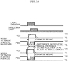
- FIG. 18 is a timing chart for describing misaligned drive timing in distance measurement driving of a conventional distance measurement device.
- the timing at which read gate TG is switched ON and the timing at which exposure reset gate PRS is switched OFF are the same, and the timing at which the read gate is switched OFF and the timing at which exposure reset gate PRS is switched ON are the same. Since these pulses are applied from the periphery of a pixel region into the pixel region, the roundness of the pulse waveform, delayed timing, etc., cause a temporal misalignment of the ON/OFF timing for read gate TG with that of exposure reset gate PRS, as illustrated in FIG.
- the present invention has been conceived in order to such problems, and aims to provide a solid-state imaging device which is small, has high distance measurement accuracy, and obtains a distance measurement signal that covers a wide distance measurement range, and provide a method for driving the solid-state imaging device.
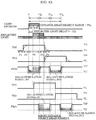
- FIG. 1 is a function block diagram illustrating an example of an outline configuration of solid-state imaging device 1000 according to Embodiment 1. As illustrated in this figure, solid-state imaging device 1000 includes imager 100, light source driver 200, drive controller 300, optical lens 400, and light source unit 500.
- Solid-state imaging device 1000 functions as a distance measurement imaging device which measures the distance to object 600, by emitting infrared light or the like from light source unit 500 toward object 600 and receiving, by imager 100, light reflected from object 600.
- Light source driver 200 generates a light emission signal instructing light irradiation to object 600.
- light source unit 500 irradiates object 600 with light using a light emission current generated by light source driver 200.
- Imager 100 includes an imaging region in which unit pixels including photoelectric conversion elements are two-dimensionally arranged, and performs exposure on a region including object 600 plural times according to timing indicated by the exposure signal generated by drive controller 300, and generates a distance measurement signal corresponding to the total amount of exposure performed plural times.
- the drive controller generates an exposure signal instructing exposure to light reflected from object 600, and calculates the distance to object 600 on the basis of the distance measurement signal received from imager 100.
- light source unit 500 emits near infrared light toward object 600 under background light, for example.
- the light reflected from object 600 enters imager 100 through optical lens 400.
- the reflected light incident on imager 100 forms an image, and the formed image is converted into an electrical signal.
- the operations of light source unit 500 and imager 100 are controlled by drive controller 300.
- the output of imager 100 is converted into a distance image, and also into a visible image depending on the usage, by drive controller 300.
- imager 100 is a solid-state imaging element such as what is called a complementary metal-oxide-semiconductor (CMOS) image sensor.
- CMOS complementary metal-oxide-semiconductor
- the solid-state imaging device according to the present invention is not required to include light source unit 500 and light source driver 200 which actively emit light toward object 600 unlike solid-state imaging device 1000 according to the present embodiment.
- the solid-state imaging device according to the present invention may obtain luminance information, etc., of object 600 by receiving external irradiating light (including natural light) reflected from object 600.
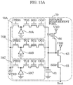
- FIG. 2 illustrates a circuit configuration of a distance measurement pixel of the solid-state imaging device according to Embodiment 1. This figure illustrates a circuit configuration of a distance measurement pixel two-dimensionally arranged in the imaging region of imager 100 according to the present embodiment. As illustrated in FIG.
- distance measurement pixel 10 includes: two unit pixels 10A and 10B which receive reflected light, photoelectrically convert the reflected light into signal charge, and accumulate and output the signal charge; one floating diffusion layer (FD) 21 which converts the signal charge into a voltage; reset (RST) transistor 24 which discharges the signal charge of FD 21 to a reset drain (VRD); amplification transistor 23 which is connected to a VDD power supply and amplifies a signal from FD 21; and selection (SEL) transistor 25 which outputs and controls a signal from amplification transistor 23 in accordance with an exteriorly obtained selection signal.
- FD floating diffusion layer
- RST reset
- VRD reset drain
- amplification transistor 23 which is connected to a VDD power supply and amplifies a signal from FD 21
- selection (SEL) transistor 25 which outputs and controls a signal from amplification transistor 23 in accordance with an exteriorly obtained selection signal.
- Each of two unit pixels 10A and 10B includes: one light receiver which receives the reflected light and photoelectrically converts the received light; one charge reset transistor which discharges, to a charge discharger, a signal obtained from the light receiver; two read transistors which read the signal from the light receiver; two charge accumulation transistors which accumulate the signal read by the two read transistors; and one or two output transistors which output the signal accumulated in the charge accumulation transistors.
- Each of the above-mentioned transistors has a structure in which a gate insulating film and a gate electrode are formed in this order above a semiconductor substrate, and can switch between a conducting state and a non-conducting state between a source and a drain using a drive pulse signal supplied from the gate electrode.
- each of the transistors or the gate electrode thereof may be referred to simply as a gate.
- unit pixel 10A includes one photoelectric conversion element 1A, read gates TG0 and TG2, charge accumulation gates SG0 and SG2, output gates OG0 and OG2, and charge reset gates PRS0.
- Unit pixel 10B includes one photoelectric conversion element 1B, read gates TG1 and TG3, charge accumulation gates SG1 and SG3, output gates OG1 and OG3, and charge reset gates PRS1.
- the number of read transistors, charge accumulation transistors, and output transistors included in one unit pixel is twice as large as that in the related art.
- These transistors can be formed within an element isolation region between the photoelectric conversion elements with the recent, finer CMOS process technology as long as the pixel size is in the range of 2 pm to 50 pm, which is typical for the TOF sensors, and thus it is possible to provide a sufficient area for the photoelectric conversion elements.
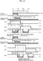
- FIG. 3 illustrates a cross-sectional structure of the unit pixel according to Embodiment 1. Specifically, the cross-sectional structure of a charge transfer path to which read gate TG2 of unit pixel 10A belongs is depicted in FIG. 3 .
- photoelectric conversion element 1A (PD0) is formed in an n-type region on a p-type substrate or a p-well, and the read transistor (RG2) and the charge reset transistor (PRS0) adjacent to photoelectric conversion element 1A (PD0) are formed in a p-type region.
- the drain (VPRD) adjacent to the charge reset transistor (PRS0) is formed in a n+-type region.
- the drain (VPRD) discharges the signal charge from photoelectric conversion element 1A (PD0) via the charge reset transistor (PRS0), and thus is connected to a VH power supply.
- the signal charge accumulated in the charge accumulation transistor (SG2) is transferred to FD 21 via the output transistor (OG2) on the same principle as a charge-coupled device, and thus the charge accumulation transistor (SG2) and the output transistor (OG2) adjacent to the read transistor (TG2) are formed with an n-type buried channel.
- Light-shielding film 30 made from a metal or a metallic compound including tungsten (W), aluminum (Al), and copper (Cu) is formed at least on the charge accumulation transistor (SG2) so as not to allow the direct entry of the reflected light, the background light, and the like at the time of signal accumulation.
- Microlens 40 is formed above light-shielding film 30 via waveguide path LP, allowing the reflected light directed to unit pixel 10A to be efficiently condensed onto photoelectric conversion element 1A (PD0).
- light-shielding film 30 may be formed above the charge reset transistor (PRS0). In the present embodiment, however, since the charge reset transistor needs to be turned ON and OFF at very high speed, light-shielding film 30 is preferably unformed, with priority placed on the property of reducing parasitic capacitance.
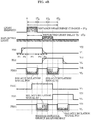
- FIG. 4A is a distance measurement drive timing chart for short-distance object measurement of the solid-state imaging device according to Embodiment 1.
- FIG. 4B is a distance measurement drive timing chart for medium-distance object measurement of the solid-state imaging device according to Embodiment 1.
- FIG. 4C is a distance measurement drive timing chart for long-distance object measurement of the solid-state imaging device according to Embodiment 1.
- FIG. 4D illustrates combinations of signals obtained by the short-distance object measurement, the medium-distance object measurement, and the long-distance object measurement.
- FIG. 5 illustrates transitions of a pixel potential distribution at the time of distance measurement driving of the unit pixel according to Embodiment 1.
- the short-distance object measurement is measurement for an object in which the delay amount of the reflected light with respect to the irradiating light is 0 to 1 Tp (short distance)
- the medium-distance object measurement is measurement for an object in which the delay amount of the reflected light with respect to the irradiating light is 1 Tp to 2 Tp (medium distance)
- the long-distance object measurement is measurement for an object in which the delay amount of the reflected light with respect to the irradiating light is 2 Tp to 3 Tp (long distance).
- drive controller 300 switches OFF read gate TG0 of unit pixel 10A and switches ON exposure reset gate PRS0 of unit pixel 10A.
- the signal charge of photoelectric conversion element 1A is discharged to drain VPRD (P1 in FIG. 5 ).
- drive controller 300 switches ON read gate TG0 (VL to VH) (P3 in FIG. 5 ).
- drive controller 300 causes exposure reset gate PRS0 to transition to ON (VL to VH) in synchronization with the end of the emission of the irradiating pulsed beam. With this, the first exposure of photoelectric conversion element 1A is completed (P4 in FIG. 5 ).
- drive controller 300 causes read gate TG0 to transition to OFF (VH to VL) (P5 in FIG. 5 ).
- the first exposure sequence is completed.
- the first exposure sequence corresponds to the first exposure operation of photoelectric conversion element 1A of unit pixel 10A in periods P1 to P5.
- drive controller 300 causes exposure reset gate PRS1 to transition to OFF (VH to VL) in synchronization with the end of the emission of the irradiating pulsed beam in period P3 mentioned above. With this, the first exposure of photoelectric conversion element 1B is started.
- drive controller 300 causes exposure reset gate PRS1 to transition to ON (VL to VH) at a point in time when period Tp (a first predetermined period of time) has elapsed since exposure reset gate PRS1 is switched OFF. With this, the first exposure of photoelectric conversion element 1B is completed.
- drive controller 300 causes read gate TG1 to transition to OFF (VH to VL).
- the second exposure sequence is completed.
- the second exposure sequence corresponds to the first exposure operation of photoelectric conversion element 1B of unit pixel 10B.
- drive controller 300 causes exposure reset gate PRS0 to transition to OFF (VH to VL). With this, the second exposure of photoelectric conversion element 1A is started.
- drive controller 300 causes exposure reset gate PRS0 to transition to ON (VL to VH) at a point in time when period Tp (the first predetermined period of time) has elapsed since exposure reset gate PRS0 is switched OFF. With this, the second exposure of photoelectric conversion element 1A is completed.
- drive controller 300 causes read gate TG2 to transition to OFF (VH to VL).
- the third exposure sequence is completed.
- the third exposure sequence corresponds to the second exposure operation of photoelectric conversion element 1A of unit pixel 10A.
- drive controller 300 causes exposure reset gate PRS1 to transition to OFF (VH to VL). With this, the second exposure of photoelectric conversion element 1B is started.
- drive controller 300 causes exposure reset gate PRS1 to transition to ON (VL to VH) at a point in time when period Tp (the first predetermined period of time) has elapsed since exposure reset gate PRS1 is switched OFF. With this, the second exposure of photoelectric conversion element 1B is completed.
- drive controller 300 causes read gate TG3 to transition to OFF (VH to VL).
- the fourth exposure sequence is completed.
- the fourth exposure sequence corresponds to the second exposure operation of photoelectric conversion element 1B of unit pixel 10B.
- drive controller 300 obtains a signal necessary for distance measurement by performing the first exposure sequence to the fourth exposure sequence.
- FIG. 4D illustrates the correlation between the signals accumulated in the charge accumulation transistors (SG0, SG1, SG2, and SG3) and the distance measurement ranges.
- reflected-light signal S0' is accumulated in the charge accumulation transistor (SG0)
- reflected-light signal S1' is accumulated in the charge accumulation transistor (SG1)
- background-light signal BG0 is accumulated in the charge accumulation transistor (SG2)
- background-light signal BG1 is accumulated in the charge accumulation transistor (SG3).
- the signal amount of S0' and S1' (the reflected-light signals) is greater than that of BG0 and BG1 (the background-light signals), and thus, by determining a combination of two charge accumulation transistors (SG) having a great amount of signals, it is possible to use different distance measurement calculation expressions for short, medium, and long distances with reference to the table illustrated in FIG. 4D , which enables seamless distance measurement covering a wide range from a short distance to a long distance.
- Distance measurement calculation expressions for obtaining distance L to object 600 at short, medium, and long distances are shown below.
- read gate TG0 and exposure reset gate PRS0 are set to VH, and all the signal charge resulting from photoelectrical conversion by photoelectric conversion element 1A is discharged to the drain (VPRD) via exposure reset gate PRS0.
- read gate TG0 is switched ON (VH) first, and after a lapse of a certain period P2, exposure reset gate PRS0 is switched OFF (VL).
- both read gate TG0 and exposure reset gate PRS0 are ON (VH), but the potential of exposure reset gate PRS0 is set higher than the potential of read gate TG0.
- the threshold voltage of exposure reset gate PRS0 is set lower than the threshold voltage of read gate TG0. Examples of this approach include setting the p-type impurity concentration of exposure reset gate PRS0 lower than the p-type impurity concentration of read gate TG0.
- a direct-current (DC) voltage of approximately 0 to (VH-VL)/2 may be superimposed on exposure reset gate PRS0.
- DC direct-current
- Examples of this approach include setting high-level potential VH' of exposure reset gate PRS0 higher than potential VH of read gate TG0.
- read gate TG0 is ON and exposure reset gate PRS0 is OFF, and all the signal charge resulting from photoelectrical conversion by photoelectric conversion element 1A is transferred, via read gate TG0, to the charge accumulation transistor (SG0), and accumulated therein; thus, the exposure in the 0 to 1 Tp period is performed.
- exposure reset gate PRS0 is switched ON, and after a lapse of a certain period P4, read gate TG0 is switched OFF; thus, the first exposure sequence is completed.
- the state of potential in period P4 is the same as the state of potential in period P2
- the state of potential in period P5 is the same as the state of potential in period P1; the same or similar operations are performed.
- Embodiment 1 the case is assumed in which light is repeatedly emitted in such a manner that the interval between the start of emission of an irradiating pulsed beam and the next start of the light emission is longer than 4 Tp.
- the present variation describes a drive method in which the interval between the start of emission of an irradiating pulsed beam and the next start of the light emission is set to 4 Tp, and the light emission and the exposure are repeatedly performed on a 4-Tp cycle.
- FIG. 7A is a distance measurement drive timing chart for longer-distance object measurement of a solid-state imaging device according to a variation of Embodiment 1.
- FIG. 7B additionally illustrates a combination of signals obtained by the longer-distance object measurement.
- FIG. 7A illustrates the case of an object in which delay time of the reflected light is 3 Tp to 4 Tp (longer distance), and the distance measurement calculation table applied at this time is as illustrated in the table in FIG. 7B .
- the charge accumulation transistor (SG3) and the charge accumulation transistor (SG0) can obtain S0' and S1' even if the delay amount of the reflected light is between 3 Tp and 4 Tp.
- FIG. 8 illustrates a circuit configuration of a distance measurement pixel of a solid-state imaging device according to Embodiment 2.
- distance measurement pixel 11 includes: one unit pixel 11A which receives reflected light, photoelectrically converts the reflected light into signal charge, and accumulates and outputs the signal charge; one FD 21 which converts the signal charge into a voltage; reset (RST) transistor 24 which discharges the signal charge of FD 21 to a reset drain (VRD); amplification transistor 23 which is connected to a VDD power supply and amplifies a signal from FD 21; and selection (SEL) transistor 25 which outputs and controls a signal from amplification transistor 23 in accordance with an exteriorly obtained selection signal.
- RST reset
- VRD reset drain
- amplification transistor 23 which is connected to a VDD power supply and amplifies a signal from FD 21
- selection (SEL) transistor 25 which outputs and controls a signal from amplification transistor 23 in accordance with an exteriorly obtained selection signal.
- One unit pixel 11A includes: one light receiver which receives the reflected light and photoelectrically converts the received light; one charge reset transistor which discharges, to a charge discharger, a signal obtained from the light receiver; four read transistors which read the signal from the light receiver; four charge accumulation transistors which accumulate the signal read by the four read transistors; and one, two, or four output transistors which output the signal accumulated in the charge accumulation transistors ( FIG. 8 illustrates the case where four output transistors are provided).
- unit pixel 11A includes one photoelectric conversion element 1, read gates TG0, TG2, TG1, and TG3, charge accumulation gates SG0, SG2, SG1, and SG3, output gates OG0, OG2, OG1, and OG3, and charge reset gate PRS.
- the number of read gates TG and the number of charge accumulation gates SG are unchanged, but the number of photoelectric conversion elements and the number of charge reset gates PRS are each reduced from two to one. Therefore, the area of the photoelectric conversion element can be approximately doubled, and the sensitivity per photoelectric conversion element is increased about twofold.
- charge reset gate PRS In order to determine the distance measurement exposure time, charge reset gate PRS needs to be switched ON and OFF at a pulse width of several ns to several hundred ns. Especially, when a short pulse width is required to improve the distance measurement accuracy, the rising edge time and the falling edge time need be no greater than several ns.
- a typical solution to this issue is to increase the width of a metal wire or provide multiple wires so that the resistance is reduced, but this causes problems such as a smaller aperture of the photoelectric conversion element and a reduction in sensitivity.
- the photoelectric conversion element can be formed with a wide aperture, compared to that in Embodiment 1.
- the sensitivity per photoelectric conversion element can be increased twofold or more.
- FIG. 9A is a distance measurement drive timing chart for short-distance object measurement of the solid-state imaging device according to Embodiment 2.
- FIG. 9B is a distance measurement drive timing chart for medium-distance object measurement of the solid-state imaging device according to Embodiment 2.
- FIG. 9C is a distance measurement drive timing chart for long-distance object measurement of the solid-state imaging device according to Embodiment 2.
- FIG. 9D illustrates combinations of signals obtained by the short-distance object measurement, the medium-distance object measurement, and the long-distance object measurement.
- FIG. 10 illustrates comparison between sequences of light emission, exposure, and reading in distance measurement driving.
- drive controller 300 switches OFF read gate TG0 of unit pixel 11A and switches ON exposure reset gate PRS0 of unit pixel 11A.
- the signal charge of photoelectric conversion element 1 is discharged to drain VPRD.
- drive controller 300 switches ON read gate TG0 (VL to VH).
- drive controller 300 causes exposure reset gate PRS to transition to OFF (VH to VL) in synchronization with the start of emission of the first irradiating pulsed beam (light emission 1). With this, the first exposure of photoelectric conversion element 1 is started.
- drive controller 300 causes read gate TG0 to transition to OFF (VH to VL).
- the first exposure sequence is completed.
- the first exposure sequence corresponds to the first exposure operation of photoelectric conversion element 1 of unit pixel 11A in periods P1 to P5.
- drive controller 300 causes exposure reset gate PRS to transition to OFF (VH to VL) at a point in time when period Tp has elapsed since exposure reset gate PRS is switched ON in the first exposure sequence. With this, the second exposure of photoelectric conversion element 1 is started.
- drive controller 300 causes exposure reset gate PRS to transition to ON (VL to VH) at a point in time when period Tp (the second predetermined period of time) has elapsed since exposure reset gate PRS is switched OFF. With this, the second exposure of photoelectric conversion element 1 is completed.
- drive controller 300 causes read gate TG2 to transition to OFF (VH to VL).
- the third exposure sequence is completed.
- the third exposure sequence corresponds to the second exposure operation of photoelectric conversion element 1 of unit pixel 11A.
- drive controller 300 causes exposure reset gate PRS to transition to OFF (VH to VL) in synchronization with the end of emission of the second irradiating pulsed beam (light emission 2). With this, the third exposure of photoelectric conversion element 1 is started.
- drive controller 300 causes exposure reset gate PRS to transition to ON (VL to VH) at a point in time when period Tp (the third predetermined period of time) has elapsed since exposure reset gate PRS is switched OFF. With this, the third exposure of photoelectric conversion element 1 is completed.
- drive controller 300 causes read gate TG1 to transition to OFF (VH to VL).
- the second exposure sequence is completed.
- the second exposure sequence corresponds to the third exposure operation of photoelectric conversion element 1 of unit pixel 11A.
- drive controller 300 causes exposure reset gate PRS to transition to OFF (VH to VL) at a point in time when period Tp has elapsed since exposure reset gate PRS is switched ON in the second exposure sequence. With this, the fourth exposure of photoelectric conversion element 1 is started.
- drive controller 300 causes exposure reset gate PRS to transition to ON (VL to VH) at a point in time when period Tp (the third predetermined period of time) has elapsed since exposure reset gate PRS is switched OFF. With this, the fourth exposure of photoelectric conversion element 1 is completed.
- drive controller 300 causes read gate TG3 to transition to OFF (VH to VL).
- the fourth exposure sequence is completed.
- the fourth exposure sequence corresponds to the fourth exposure operation of photoelectric conversion element 1 of unit pixel 11A.
- the first exposure sequence, the third exposure sequence, the second exposure sequence, and the fourth exposure sequence are sequentially performed, and thus drive controller 300 obtains a signal necessary for distance measurement.
- the sensitivity per photoelectric conversion element is increased to a value greater than or equal to twice that in Embodiment 1, and therefore the length of emission of the first irradiating pulsed beam (light emission 1) and the length of emission of the second irradiating pulsed beam (light emission 2) can each be reduced to half or less.
- the total length of light emission can be kept to less than or equal to the total length of light emission in the related art and Embodiment 1.
- the second irradiating pulsed beam (light emission 2) preferably has the same pulse width as the first irradiating pulsed beam (light emission 2).
- the first irradiating pulsed beam (light emission 1) is repeated several hundred to several million times, and then the second irradiating pulsed beam (light emission 2) is repeated the same number of times before the transition to reading.
- light emission 1 and light emission 2 which are repeated a small number of times may be alternately performed plural times before the transition to reading (Variation of Embodiment 2).
- the temporal difference between the exposure in light emission 1 and the exposure in light emission 2 can be smaller than that in Embodiment 2.
- distance measurement error on an edge portion of the object due to this temporal difference can be inhibited.
- the distance measurement calculation expressions for determining distance L to object 600 at short, medium, and long distances according to the present embodiment and the variation thereof are the same as those in Equations 5 to 10 indicated in Embodiment 1.
- reflected-light signal S0' is accumulated in the charge accumulation transistor (SG0)
- reflected-light signal S1' is accumulated in the charge accumulation transistor (SG1)
- background-light signal BG0 is accumulated in the charge accumulation transistor (SG2)
- background-light signal BG1 is accumulated in the charge accumulation transistor (SG3).
- the signal amount of S0' and S1' (the reflected-light signals) is greater than that of BG0 and BG1 (the background-light signals), and thus, by determining a combination of two charge accumulation transistors (SG) having a great amount of signals, it is possible to use different distance measurement calculation expressions for short, medium, and long distances with reference to the table illustrated in FIG. 9D , which enables seamless distance measurement covering a wide range from a short distance to a long distance.
- FIG. 11 illustrates transitions of a pixel potential distribution at the time of distance measurement driving of a unit pixel according to Embodiment 2.
- the potential change of the unit pixel at the time of exposure according to Embodiment 2 is basically the same as that according to Embodiment 1.
- read gate TG0 is set to VL
- exposure reset gate PRS is set to VH
- all the signal charge resulting from photoelectrical conversion by photoelectric conversion element 1 is discharged to the drain (VPRD) via exposure reset gate PRS.
- read gate TG0 is switched ON (VH) first, and after a lapse of a certain period P2, exposure reset gate PRS is switched OFF (VL).
- the threshold voltage of exposure reset gate PRS is set lower than the threshold voltage of read gate TG0.
- this approach include setting the p-type impurity concentration of exposure reset gate PRS lower than the p-type impurity concentration of read gate TG0.
- a DC voltage of approximately 0 to (VH-VL)/2 may be superimposed on exposure reset gate PRS0. Examples of this approach include setting high-level potential VH' of exposure reset gate PRS0 higher than potential VH of read gate TG0.
- read gate TG0 is ON and exposure reset gate PRS is OFF, and all the signal charge resulting from photoelectrical conversion by photoelectric conversion element 1 is transferred, via read gate TG0, to the charge accumulation transistor (SG0), and accumulated therein; thus, the exposure in the 0 to 1 Tp period is performed.
- exposure reset gate PRS is switched ON, and after a lapse of a certain period P4, read gate TG0 is switched OFF; thus, the first exposure sequence is completed.
- the state of potential in period P4 is the same as the state of potential in period P2
- the state of potential in period P5 is the same as the state of potential in period P1; the same or similar operations are performed.
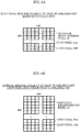
- FIG. 12A illustrates that the solid-state imaging device according to Embodiment 2 can reduce the optical size
- FIG. 12B illustrates that the solid-state imaging device according to Embodiment 2 can enlarge the unit pixel size twice that in the related art
- FIG. 12C illustrates that the solid-state imaging device according to Embodiment 2 can enlarge the unit pixel size to three times that in the related art.
- FIG. 12A compared to the related art, when the unit pixel size is made the same, the distance measurement pixel size can be reduced, and thus the optical size can be reduced.
- the unit pixel size can be set to twice that in the related art.
- FIG. 12C when the optical size is set equivalent to that in the related art, the unit pixel size can be set to three times that in the related art, allowing significant improvements to pixel properties such as sensitivity and saturation.
- the number of read gates TG and the number of charge accumulation gates SG are unchanged, but the number of photoelectric conversion elements and the number of charge reset gates PRS are each reduced from two to one. Therefore, the area of the photoelectric conversion element can be approximately doubled, and the sensitivity per photoelectric conversion element is increased about twofold.
- charge reset gate PRS needs to be switched ON and OFF at a pulse width of several ns to several hundred ns. Especially, when a short pulse width is required to improve the distance measurement accuracy, the rising edge time and the falling edge time need be no greater than several ns.
- the photoelectric conversion element can be formed with a wide aperture, compared to that in Embodiment 1.
- the sensitivity per photoelectric conversion element can be increased twofold or more.
- FIG. 13A is a distance measurement drive timing chart for longer-distance object measurement of a solid-state imaging device according to a variation of Embodiment 2.
- FIG. 12B additionally illustrates a combination of signals obtained by the longer-distance object measurement.
- FIG. 13A illustrates the case of an object in which delay time of the reflected light is 3 Tp to 4 Tp (longer distance), and the distance measurement calculation table applied at this time is as illustrated in the table in FIG. 13B .
- Embodiment 2 describes the case where light is repeatedly emitted in such a manner that the interval between the start of light emission and the next start of the light emission is longer than 4 Tp
- the present variation describes the case where the interval between the start of light emission and the next start of the light emission is set to 4 Tp, and the light emission and the exposure are repeatedly performed on a 4-Tp cycle.
- the charge accumulation transistor (SG3) and the charge accumulation transistor (SG0) can obtain S0' and S1' even if the delay amount of the reflected light is between 3 Tp and 4 Tp.
- the solid-state imaging device and the method for driving the same according to the present disclosure have been described thus far based on the above embodiments, the solid-state imaging device and the method for driving the same according to the present disclosure are not limited to the embodiments described above.
- the present invention includes other embodiments implemented through a combination of arbitrary structural elements of the above embodiments, or variations obtained through the application of various modifications to the above embodiments that may be conceived by a person having ordinary skill in the art, without departing from the essence of the present invention, and various devices such as a distance measurement imaging device in which the solid-state imaging device according to the present disclosure is built-in.
- the charge reset transistor which discharges, to the charge discharger, the signal obtained from the light receiver in the unit pixel according to Embodiment 2 is formed of a metal-oxide-semiconductor (MOS) transistor including an insulating film and a gate electrode film formed above the semiconductor substrate, but this charge reset transistor may be formed of an npn bipolar transistor, which is often used in an interline-transfer capacitive coupling element, as illustrated in FIG. 14 .
- MOS metal-oxide-semiconductor
- FIG. 14 illustrates a cross-sectional structure of a unit pixel according to another embodiment.
- n-type photoelectric conversion element 1A (PD0) serves as an emitter portion
- p-well serves as a base portion
- an n-type substrate electrode (VSUB) serves as a collector portion.
- the p-well of the base portion is grounded, and when high-level voltage VH' is applied to the n-type substrate electrode (VSUB) of the collector portion, the signal charge resulting from photoelectric conversion by photoelectric conversion element 1A is discharged to n-type substrate electrode VSUB via the p-well.
- the parasitic capacitance between the p-well and substrate electrode VSUB is significantly reduced, compared to the parasitic capacitance between exposure reset gate PRS0 and the drain (VPRD) according to Embodiment 2, and furthermore, when the n-type substrate electrode has a high n-type impurity concentration, the substrate resistance of the n-type substrate electrode is significantly reduced; thus, it is possible to make significant improvements to the roundness of the waveform of exposure reset pulse, the delayed timing, etc., that are caused by such parasitic capacitance and substrate resistance.
- the solid-state imaging device according to the present invention is not required to include light source unit 500 and light source driver 200 which actively emit light toward object 600 unlike solid-state imaging device 1000 according to the present embodiment.
- the solid-state imaging device according to the present invention may obtain luminance information, etc., of object 600 by receiving external irradiating light (including natural light) reflected from object 600.
- a method for driving a solid-state imaging device including a plurality of unit pixels arranged on a semiconductor substrate and each including: a photoelectric converter; a charge discharger; an exposure resetter which switches timing for accumulating charge in photoelectric converter and timing for discharging the charge from the photoelectric converter to the charge discharger; n charge accumulators which accumulate the charge of the photoelectric converter where n is a natural number; n readers which are provided between the photoelectric converter and the n charge accumulators and read the charge from the photoelectric converter to the charge accumulators; and an outputter which outputs the charge accumulated in the n charge accumulators.
- the method for driving a solid-state imaging device includes repeating an exposure sequence n times, including: a first reading conduction step of placing the n-th reader in a conducting state in the n-th exposure sequence; a first exposure start step of placing the exposure resetter in a non-conducting state after a lapse of a predetermined period of time starting from the first reading conduction step, and starting exposure of the photoelectric converter; a first exposure stop step of placing the exposure resetter in a conducting state after the first exposure start step, and stopping the exposure of the photoelectric converter; and a first reading non-conduction step of placing the n-th reader in a non-conducting state after a lapse of a predetermined period of time starting from the first exposure stop step.
- the abovementioned plurality of unit pixels may include m unit pixels each of which performs the exposure sequence n times to obtain a maximum of m ⁇ n signals having different exposure periods.
- the present invention is useful, for example, for a gesture user interface which detects movement of a person, an intrusion detection sensor which detects an object, a person, or the like entering the distance measurement range, and a three-dimensional input device which collects accurate data on the shape of an object in real-time.
Landscapes
- Engineering & Computer Science (AREA)
- Physics & Mathematics (AREA)
- General Physics & Mathematics (AREA)
- Power Engineering (AREA)
- Electromagnetism (AREA)
- Remote Sensing (AREA)
- Computer Networks & Wireless Communication (AREA)
- Radar, Positioning & Navigation (AREA)
- Condensed Matter Physics & Semiconductors (AREA)
- Computer Hardware Design (AREA)
- Microelectronics & Electronic Packaging (AREA)
- Signal Processing (AREA)
- Multimedia (AREA)
- Optical Radar Systems And Details Thereof (AREA)
- Transforming Light Signals Into Electric Signals (AREA)
- Solid State Image Pick-Up Elements (AREA)
- Measurement Of Optical Distance (AREA)
Abstract
Description
- The present invention relates to methods for driving solid-state imaging devices to be used in imaging for distance measurement.
- Among methods for sensing an object, the time of flight (TOF) method is known in which a distance is measured using flight time that light takes to travel to and return from a measurement object.
- Patent Literature (PTL) 1 discloses a distance image sensor in which two different signal storage units store signals obtained by transfer of charge with different phases in synchronization with intermittent behavior of light from a light source, the distance to an object is determined using the distribution ratio of the stored signals, and furthermore, a third signal storage unit stores signals of background light only, and thus background light removal is performed to eliminate the impact of the background light.
- PTL 1: Japanese Unexamined Patent Application Publication No.
2004-294420 - In a general pulse TOF method, exposure periods T1 to T3 are set to have the same length as pulse width Tp where T1 is a first exposure period starting from time of a rising edge of irradiating light having pulse width Tp, T2 is a second exposure period starting from time of a falling edge of the irradiating light, and T3 is a third exposure period in which exposure is performed in a state where the irradiating light is OFF. Suppose that the amount of signals obtained by an imager during first exposure period T1 is denoted as A0, the amount of signals obtained by the imager during second exposure period T2 is denoted as A1, the amount of signals obtained by the imager during third exposure period T3 is denoted as A2, and the speed of light (299,792,458 m/s) is denoted as c, distance L is given by the following equation.

- The solid-state imaging device used in the distance measurement imaging device using this TOF method repeats, more than one time, sampling that is performed for one period of the irradiating light. In the abovementioned TOF method, distance measurement range D is represented as follows.

- Meanwhile, in
PTL 1, when a pixel that obtains background light is taken into account, a distance is calculated using three pixels as one distance measurement unit, and thus one distance measurement unit for calculating a distance is large, meaning that downsizing is difficult to achieve. Furthermore, since each pixel includes only one charge accumulator, an increase in the pulse width (To) of the light source leads to an increase in distance measurement range D, but causes a decrease in distance resolution. In other words, the distance measurement accuracy is inversely proportional to the pulse width (To) of the light source; when the pulse width (To) of the light source is increased in order to widen the distance measurement range (limit) D, conversely, the distance measurement accuracy is decreased. Furthermore, distance measurement variation becomes large as a result of variation in signals of background light due to the production tolerance of each pixel. - In view of the abovementioned problems, the present invention has an object to provide a method for driving a solid-state imaging device which is small, has high distance measurement accuracy, and obtains a distance measurement signal that covers a wide distance measurement range.
- In order to solve the abovementioned problems, a method for driving a solid-state imaging device according to an aspect of the present invention is a method for driving a solid-state imaging device which captures a distance measurement image for measuring a distance to an object irradiated with a pulsed beam having a predetermined pulse width and includes, on a semiconductor substrate, a unit pixel including: a photoelectric converter which receives reflected light from the object and converts the reflected light into charge; a charge discharger which discharges the charge of the photoelectric converter; an exposure resetter which switches timing for accumulating the charge in the photoelectric converter and timing for discharging the charge from the photoelectric converter to the charge discharger; n charge accumulators which accumulate the charge of the photoelectric converter where n is a natural number; and n readers which are provided between the photoelectric converter and the n charge accumulators and read the charge from the photoelectric converter to the n charge accumulators where n is a natural number. The method for driving the solid-state imaging device includes performing an exposure sequence including: an exposure start step of starting exposure of the photoelectric converter by placing the exposure resetter in a non-conducting state after a lapse of a predetermined period of time starting when the n readers are placed in a conducting state; and an exposure stop step of stopping the exposure of the photoelectric converter by placing the exposure resetter in the conducting state a predetermined period of time before placing the n readers in the non-conducting state after the exposure is started.
- With the method for driving a solid-state imaging device according to the present invention, a small solid-state imaging device can obtain a distance measurement signal that covers a wide distance measurement range with high distance measurement accuracy.
-
-
FIG. 1 is a function block diagram illustrating an example of an outline configuration of a solid-state imaging device according toEmbodiment 1. -
FIG. 2 illustrates a circuit configuration of a distance measurement pixel of a solid-state imaging device according toEmbodiment 1. -
FIG. 3 illustrates a cross-sectional structure of a unit pixel according toEmbodiment 1. -
FIG. 4A is a distance measurement drive timing chart for short-distance measurement of a solid-state imaging device according toEmbodiment 1. -
FIG. 4B is a distance measurement drive timing chart for medium-distance measurement of a solid-state imaging device according toEmbodiment 1. -
FIG. 4C is a distance measurement drive timing chart for long-distance measurement of a solid-state imaging device according toEmbodiment 1. -
FIG. 4D illustrates combinations of signals obtained by short-distance measurement, medium-distance measurement, and long-distance measurement. -
FIG. 5 illustrates transitions of a pixel potential distribution at the time of distance measurement driving of a unit pixel according toEmbodiment 1. -
FIG. 6A illustrates that a solid-state imaging device according toEmbodiment 1 can reduce an optical size. -
FIG. 6B illustrates that a solid-state imaging device according toEmbodiment 1 can enlarge a unit pixel size. -
FIG. 7A is a distance measurement drive timing chart for longer-distance measurement of a solid-state imaging device according to a variation ofEmbodiment 1. -
FIG. 7B additionally illustrates a combination of signals obtained by longer-distance measurement. -
FIG. 8 illustrates a circuit configuration of a distance measurement pixel of a solid-state imaging device according toEmbodiment 2. -
FIG. 9A is a distance measurement drive timing chart for short-distance measurement of a solid-state imaging device according toEmbodiment 2. -
FIG. 9B is a distance measurement drive timing chart for medium-distance measurement of a solid-state imaging device according toEmbodiment 2. -
FIG. 9C is a distance measurement drive timing chart for long-distance measurement of a solid-state imaging device according toEmbodiment 2. -
FIG. 9D illustrates combinations of signals obtained by short-distance measurement, medium-distance measurement, and long-distance measurement. -
FIG. 10 illustrates comparison between sequences of light emission, exposure, and reading in distance measurement driving. -
FIG. 11 illustrates transitions of a pixel potential distribution at the time of distance measurement driving of a unit pixel according toEmbodiment 2. -
FIG. 12A illustrates that a solid-state imaging device according toEmbodiment 2 can reduce an optical size. -
FIG. 12B illustrates that a solid-state imaging device according toEmbodiment 2 can enlarge a unit pixel size by a factor of 2. -
FIG. 12C illustrates that a solid-state imaging device according toEmbodiment 2 can enlarge a unit pixel size by a factor of 3. -
FIG. 13A is a distance measurement drive timing chart for longer-distance measurement of a solid-state imaging device according to a variation ofEmbodiment 2. -
FIG. 13B additionally illustrates a combination of signals obtained by longer-distance measurement. -
FIG. 14 illustrates a cross-sectional structure of a unit pixel according to another embodiment. -
FIG. 15A is a schematic configuration view of a conventional distance measurement pixel which obtains distance measurement information using three unit pixels. -
FIG. 15B is a timing chart for describing distance measurement driving of a conventional distance measurement device. -
FIG. 16 illustrates transitions of a pixel potential distribution at the time of distance measurement driving of a conventional distance measurement device. -
FIG. 17 illustrates the arrangement of a conventional distance measurement pixel which obtains distance measurement information using three unit pixels. -
FIG. 18 is a timing chart for describing misaligned drive timing in distance measurement driving of a conventional distance measurement device. - The inventors have found the following problems with the distance image sensor disclosed in the Background Art section. Hereinafter, the problems will be described with reference to the drawings.
- In the distance image sensor disclosed in
PTL 1, three unit pixel groups are used in such a way that three exposure processes are performed at different timings for one light emission and reflected light thereof, and thus distance information is obtained from such three exposure signals for each set of three unit pixels (= distance measurement pixels). -
FIG. 15A is a schematic configuration view of a conventional distance measurement pixel which obtains distance measurement information using three unit pixels.FIG. 15B is a timing chart for describing distance measurement driving of a conventional distance measurement device.FIG. 16 illustrates transitions of a pixel potential distribution at the time of distance measurement driving of the conventional distance measurement device. InFIG. 15A , structural elements of threeunit pixels unit pixels distance measurement pixel 70.Unit pixel 70A includes onephotoelectric conversion element 50A, read gate TG0, charge accumulation gate SG0, output gate OG0, and exposure reset gate PRS0.Unit pixel 70B includes onephotoelectric conversion element 50B, a read gate TG1, charge accumulation gate SG1, output gate OG1, and exposure reset gate PRS1.Unit pixel 70C includes onephotoelectric conversion element 50C, read gate TG2, charge accumulation gate SG2, output gate OG2, and exposure reset gate PRS2. Furthermore,distance measurement pixel 70 includes: floating diffusion (FD) 61 which is shared by threeunit pixels amplification transistor 63; resettransistor 64; andselection transistor 65. - In
distance measurement pixel 70 having the abovementioned configuration, as illustrated inFIG. 15B , at the time of exposure of each photoelectric conversion element, the operation of starting the signal reading from the photoelectric conversion element to the charge accumulation gate and the operation of stopping the signal discharge from the photoelectric conversion element to drain VPRD are performed at the same time. Furthermore, the operation of stopping the signal reading from the photoelectric conversion element to the charge accumulation gate and the operation of starting the signal discharge from the photoelectric conversion element to drain VPRD are performed at the same time. Next, distance measurement driving of the conventional distance measurement device will be described. - As illustrated in
FIG. 15B , first, in period P1, read gate TG0 ofunit pixel 70A (S0 exposure pixel) is OFF, exposure reset gate PRS0 is ON, and signal charge ofphotoelectric conversion element 50A is discharged to drain VPRD (P1 inFIG. 16 : discharge). - Next, in period P2, in synchronization with switching ON of a light emission pulse, read gate TG0 is switched ON (VL to VH), and exposure reset gate PRS0 is switched OFF (VH to VL); thus, the signal charge of
photoelectric conversion element 50A is transferred to charge accumulation gate SG0 and accumulated therein (P2 inFIG. 16 : accumulation). - Next, in synchronization with switching OFF of the light emission pulse, read gate TG0 is switched OFF again (VH to VL), and exposure reset gate PRS0 is switched ON (VL to VH); thus, the charge of
photoelectric conversion element 50A is discharged to drain VPRD, resulting in completion of S0 exposure sequence atunit pixel 70A. - Next, in period P3, at
unit pixel 70B (S1 exposure pixel), in the same manner as withunit pixel 70A, read gate TG1 is OFF, exposure reset gate PRS1 is ON, and signal charge ofphotoelectric conversion element 50B is discharged to drain VPRD (P3 inFIG. 16 : discharge). - Next, in period P3, in synchronization with switching OFF of a light emission pulse, read gate TG1 is switched ON (VL to VH), and exposure reset gate PRS1 is switched OFF (VH to VL); thus, the signal charge of
photoelectric conversion element 50B is transferred to charge accumulation gate SG1 and accumulated therein. - Next, after the lapse of the same exposure period as that of the S0 exposure at
unit pixel 70A, read gate TG1 is switched OFF again (VH to VL), and exposure reset gate PRS1 is switched ON (VL to VH); thus, the charge ofphotoelectric conversion element 50B is discharged to drain VPRD, resulting in completion of S1 exposure sequence atunit pixel 70B. - Next, at
unit pixel 70C (BG exposure pixel), in the same manner as withunit pixel 70A, read gate TG2 is OFF, exposure reset gate PRS2 is ON, and signal charge ofphotoelectric conversion element 50C is discharged to drain VPRD. - Next, in a period in which no reflected light pulse is present (only background (BG) light is present), read gate TG2 is switched ON (VL to VH), and exposure reset gate PRS2 is switched OFF (VH to VL); thus, the signal charge of
photoelectric conversion element 50C is transferred to charge accumulation gate SG2 and accumulated therein. - Next, after the lapse of the same period as the S0 exposure period at
unit pixel 70A and the same period as the S1 exposure period atunit pixel 70B, read gate TG2 is switched OFF again (VH to VL), and exposure reset gate PRS2 is switched ON (VL to VH); thus, the charge ofphotoelectric conversion element 50C is discharged to drain VPRD, resulting in completion of BG exposure sequence atunit pixel 70C. - The abovementioned S0 exposure sequence, S1 exposure sequence, and BG exposure sequence are repeated several hundred to several hundred thousand times, the amount of accumulated signals in a charge accumulation transistor having charge accumulation gate SG is increased, and thereafter output gate OG is switched ON so that the charge accumulated in the charge accumulation transistor is transferred, and charge accumulation gate SG is switched OFF and output gate OG is switched OFF in sequence so that all of the accumulated charge is transferred and output to
FD 61. - In other words, in the above-described conventional distance measurement driving, three unit pixels form one distance measurement pixel, and distance measurement calculation is performed through one light emission and three exposure processes using three unit pixels.
- Using the signals obtained by the above-described distance measurement driving, distance L to a subject can be calculated on a per-distance-measurement-pixel basis according to
Equation 1 to Equation 4 below. In the equations, S0' represents the signal charge accumulated in charge accumulation gate SG0 in the S0 exposure sequence atunit pixel 70A, S1' represents the signal charge accumulated in charge accumulation gate SG1 in the S1 exposure sequence atunit pixel 70B, and BG2 represents the signal charge accumulated in charge accumulation gate SG2 in the BG exposure sequence atunit pixel 70C.
[Math. 1]


- Since S0 + S1 obtained by removing background light (BG2) components corresponds to light emission pulse width Tp and S1 is proportional to time of flight (TOF) of the reflected light, distance L to the subject can be calculated on a per-distance-measurement-pixel basis according to
Equation 1 to Equation 4. - The conventional distance measurement device described above, however, has the following problems.
-
FIG. 17 illustrates the arrangement of a conventional distance measurement pixel which obtains distance measurement information using three unit pixels. Recent years have seen a sharp rise in the demand for small, high-resolution (at least QVGA) TOF sensors for a machine vision application, a gesture input application, etc., in the field of mobile, robot, and vehicle-mounted devices, for example. Accordingly, the realization of small, high-resolution TOF sensors capable of measuring a distance using miniaturized distance measurement pixels is awaited. - In the related art, however, as illustrated in
FIG. 17 , each unit pixel performs one accumulation, and therefore three unit pixels are needed to obtain three signals (S0', S1', BG) required for distance measurement, causing an increase in the size of the distance measurement pixel. Thus, in order to obtain high resolutions that have been demanded in recent years, such as VGA and SXGA, the optical size of the TOF sensor needs to be increased, as illustrated inFIG. 17 . - As illustrated in the circuit diagram of the distance measurement pixel in
FIG. 15A and the distance measurement drive timing inFIG. 15B , when S0 and S1 to be used in Equation 4 for calculating distance L are derived fromEquation 1, the BG component is subtracted using BG2 accumulated in the charge accumulation transistor ofunit pixel 70C. In this regard, respective background light components actually contained in S0' and S1' are signals BG0 and BG1 obtained by the exposure ofunit pixel unit pixel 70C. - Therefore, when S0 and S1 are calculated using
Equation 1, variations in the sensitivity of photoelectric conversion elements, the dark current, and the exposure reset pulses (exposure variations) that are caused by the production tolerance of respective unit pixels affect BG0, BG1, and BG2, resulting in increased distance measurement variations. - When the distance to the subject is great, the delay amount of the reflected light is large, and at a point in time later than the end of the exposure period for exposure reset gate PRS1, BG is mixed with the reflected light, causing a change in the values of S0 and S1 after the subtraction of BG in
Equation 1; thus, the distance measurement calculation becomes inaccurate. - Therefore, in the related art, only a short distance (c•Tp/2) corresponding to 1 Tp can be measured. For example, when Tp = 11 ns, maximum distance measurement range Zmax is limited to 1.65 m.
-
FIG. 18 is a timing chart for describing misaligned drive timing in distance measurement driving of a conventional distance measurement device. As illustrated inFIG. 15B , in the related art, the timing at which read gate TG is switched ON and the timing at which exposure reset gate PRS is switched OFF are the same, and the timing at which the read gate is switched OFF and the timing at which exposure reset gate PRS is switched ON are the same. Since these pulses are applied from the periphery of a pixel region into the pixel region, the roundness of the pulse waveform, delayed timing, etc., cause a temporal misalignment of the ON/OFF timing for read gate TG with that of exposure reset gate PRS, as illustrated inFIG. 17 , and thus there may be a large difference in exposure time, exposure timing, and the like (1 ns misalignment causes a 15 cm difference in measured distance). As a result, in the imaging plane, the amount of signals S0, S1, and BG varies, and distance measurement variations, offset, and shading occur. - The present invention has been conceived in order to such problems, and aims to provide a solid-state imaging device which is small, has high distance measurement accuracy, and obtains a distance measurement signal that covers a wide distance measurement range, and provide a method for driving the solid-state imaging device.
- Hereinafter, solid-state imaging devices and methods for driving the same according to the embodiments of the present disclosure will be described with reference to the drawings. Note that each of the following embodiments shows one specific example of the present invention; the numerical values, shapes, materials, structural elements, the arrangement and connection of the structural elements, etc., shown in the following embodiments are mere examples, and are not intended to limit the present invention.
-
FIG. 1 is a function block diagram illustrating an example of an outline configuration of solid-state imaging device 1000 according toEmbodiment 1. As illustrated in this figure, solid-state imaging device 1000 includesimager 100,light source driver 200,drive controller 300,optical lens 400, andlight source unit 500. - Solid-
state imaging device 1000 according to the present embodiment functions as a distance measurement imaging device which measures the distance to object 600, by emitting infrared light or the like fromlight source unit 500 towardobject 600 and receiving, byimager 100, light reflected fromobject 600. -
Light source driver 200 generates a light emission signal instructing light irradiation to object 600. - In accordance with the light emission signal generated by
drive controller 300,light source unit 500 irradiatesobject 600 with light using a light emission current generated bylight source driver 200. -
Imager 100 includes an imaging region in which unit pixels including photoelectric conversion elements are two-dimensionally arranged, and performs exposure on aregion including object 600 plural times according to timing indicated by the exposure signal generated bydrive controller 300, and generates a distance measurement signal corresponding to the total amount of exposure performed plural times. - The drive controller generates an exposure signal instructing exposure to light reflected from
object 600, and calculates the distance to object 600 on the basis of the distance measurement signal received fromimager 100. - As illustrated in
FIG. 1 ,light source unit 500 emits near infrared light towardobject 600 under background light, for example. The light reflected fromobject 600 entersimager 100 throughoptical lens 400. The reflected light incident onimager 100 forms an image, and the formed image is converted into an electrical signal. The operations oflight source unit 500 andimager 100 are controlled bydrive controller 300. The output ofimager 100 is converted into a distance image, and also into a visible image depending on the usage, bydrive controller 300. One example ofimager 100 is a solid-state imaging element such as what is called a complementary metal-oxide-semiconductor (CMOS) image sensor. - Note that the solid-state imaging device according to the present invention is not required to include
light source unit 500 andlight source driver 200 which actively emit light towardobject 600 unlike solid-state imaging device 1000 according to the present embodiment. The solid-state imaging device according to the present invention may obtain luminance information, etc., ofobject 600 by receiving external irradiating light (including natural light) reflected fromobject 600. -
FIG. 2 illustrates a circuit configuration of a distance measurement pixel of the solid-state imaging device according toEmbodiment 1. This figure illustrates a circuit configuration of a distance measurement pixel two-dimensionally arranged in the imaging region ofimager 100 according to the present embodiment. As illustrated inFIG. 2 ,distance measurement pixel 10 includes: twounit pixels transistor 24 which discharges the signal charge ofFD 21 to a reset drain (VRD);amplification transistor 23 which is connected to a VDD power supply and amplifies a signal fromFD 21; and selection (SEL)transistor 25 which outputs and controls a signal fromamplification transistor 23 in accordance with an exteriorly obtained selection signal. - Each of two
unit pixels - More specifically,
unit pixel 10A includes onephotoelectric conversion element 1A, read gates TG0 and TG2, charge accumulation gates SG0 and SG2, output gates OG0 and OG2, and charge reset gates PRS0.Unit pixel 10B includes onephotoelectric conversion element 1B, read gates TG1 and TG3, charge accumulation gates SG1 and SG3, output gates OG1 and OG3, and charge reset gates PRS1. - Note that in the configuration of the distance measurement pixel according to the present embodiment, the number of read transistors, charge accumulation transistors, and output transistors included in one unit pixel is twice as large as that in the related art. These transistors, however, can be formed within an element isolation region between the photoelectric conversion elements with the recent, finer CMOS process technology as long as the pixel size is in the range of 2 pm to 50 pm, which is typical for the TOF sensors, and thus it is possible to provide a sufficient area for the photoelectric conversion elements.
- Furthermore, as a result of an increase in the number of such transistors, even if the area of the photoelectric conversion element is slightly reduced, introduction of an on-chip microlens and a waveguide path on the pixel allows the reflected light directed to the receiver to be efficiently guided to the photoelectric conversion element, as illustrated in the cross-sectional structure of the unit pixel (
FIG. 3 ) to be described later. With this, it is possible to inhibit a reduction in pixel properties such as sensitivity degradation and saturation. -
FIG. 3 illustrates a cross-sectional structure of the unit pixel according toEmbodiment 1. Specifically, the cross-sectional structure of a charge transfer path to which read gate TG2 ofunit pixel 10A belongs is depicted inFIG. 3 . As illustrated inFIG. 3 ,photoelectric conversion element 1A (PD0) is formed in an n-type region on a p-type substrate or a p-well, and the read transistor (RG2) and the charge reset transistor (PRS0) adjacent tophotoelectric conversion element 1A (PD0) are formed in a p-type region. The drain (VPRD) adjacent to the charge reset transistor (PRS0) is formed in a n+-type region. The drain (VPRD) discharges the signal charge fromphotoelectric conversion element 1A (PD0) via the charge reset transistor (PRS0), and thus is connected to a VH power supply. - The signal charge accumulated in the charge accumulation transistor (SG2) is transferred to
FD 21 via the output transistor (OG2) on the same principle as a charge-coupled device, and thus the charge accumulation transistor (SG2) and the output transistor (OG2) adjacent to the read transistor (TG2) are formed with an n-type buried channel. Light-shieldingfilm 30 made from a metal or a metallic compound including tungsten (W), aluminum (Al), and copper (Cu) is formed at least on the charge accumulation transistor (SG2) so as not to allow the direct entry of the reflected light, the background light, and the like at the time of signal accumulation. -
Microlens 40 is formed above light-shieldingfilm 30 via waveguide path LP, allowing the reflected light directed tounit pixel 10A to be efficiently condensed ontophotoelectric conversion element 1A (PD0). Note that light-shieldingfilm 30 may be formed above the charge reset transistor (PRS0). In the present embodiment, however, since the charge reset transistor needs to be turned ON and OFF at very high speed, light-shieldingfilm 30 is preferably unformed, with priority placed on the property of reducing parasitic capacitance. - The drive timing for distance measurement pixels according to the present embodiment will be described with reference to
FIG. 4A to FIG. 4D andFIG. 5 . -
FIG. 4A is a distance measurement drive timing chart for short-distance object measurement of the solid-state imaging device according toEmbodiment 1.FIG. 4B is a distance measurement drive timing chart for medium-distance object measurement of the solid-state imaging device according toEmbodiment 1.FIG. 4C is a distance measurement drive timing chart for long-distance object measurement of the solid-state imaging device according toEmbodiment 1.FIG. 4D illustrates combinations of signals obtained by the short-distance object measurement, the medium-distance object measurement, and the long-distance object measurement.FIG. 5 illustrates transitions of a pixel potential distribution at the time of distance measurement driving of the unit pixel according toEmbodiment 1. - Assuming that Tp represents the pulse width of the irradiating light, the short-distance object measurement is measurement for an object in which the delay amount of the reflected light with respect to the irradiating light is 0 to 1 Tp (short distance), the medium-distance object measurement is measurement for an object in which the delay amount of the reflected light with respect to the irradiating light is 1 Tp to 2 Tp (medium distance), and the long-distance object measurement is measurement for an object in which the delay amount of the reflected light with respect to the irradiating light is 2 Tp to 3 Tp (long distance).
- As illustrated in
FIG. 4A to FIG. 4C , first, in period P1,drive controller 300 switches OFF read gate TG0 ofunit pixel 10A and switches ON exposure reset gate PRS0 ofunit pixel 10A. Thus, the signal charge ofphotoelectric conversion element 1A is discharged to drain VPRD (P1 inFIG. 5 ). - Next, in period P2,
drive controller 300 switches ON read gate TG0 (VL to VH) (P3 inFIG. 5 ). - Next, in period P3,
drive controller 300 causes exposure reset gate PRS0 to transition to OFF (VH to VL) in synchronization with the start of emission of an irradiating pulsed beam. With this, the first exposure ofphotoelectric conversion element 1A is started (P3 inFIG. 5 ). - Next, in period P4,
drive controller 300 causes exposure reset gate PRS0 to transition to ON (VL to VH) in synchronization with the end of the emission of the irradiating pulsed beam. With this, the first exposure ofphotoelectric conversion element 1A is completed (P4 inFIG. 5 ). - Next, in period P5,
drive controller 300 causes read gate TG0 to transition to OFF (VH to VL) (P5 inFIG. 5 ). - Thus, the first exposure sequence is completed. In other words, the first exposure sequence corresponds to the first exposure operation of
photoelectric conversion element 1A ofunit pixel 10A in periods P1 to P5. - Next, in the state where read gate TG1 of
unit pixel 10B is ON (VL to VH) and a new irradiating pulsed beams is not emitted,drive controller 300 causes exposure reset gate PRS1 to transition to OFF (VH to VL) in synchronization with the end of the emission of the irradiating pulsed beam in period P3 mentioned above. With this, the first exposure ofphotoelectric conversion element 1B is started. - Next,
drive controller 300 causes exposure reset gate PRS1 to transition to ON (VL to VH) at a point in time when period Tp (a first predetermined period of time) has elapsed since exposure reset gate PRS1 is switched OFF. With this, the first exposure ofphotoelectric conversion element 1B is completed. - Next,
drive controller 300 causes read gate TG1 to transition to OFF (VH to VL). - Thus, the second exposure sequence is completed. In other words, the second exposure sequence corresponds to the first exposure operation of
photoelectric conversion element 1B ofunit pixel 10B. - Next, in the state where read gate TG2 of
unit pixel 10A is ON (VL to VH),drive controller 300 causes exposure reset gate PRS0 to transition to OFF (VH to VL). With this, the second exposure ofphotoelectric conversion element 1A is started. - Next,
drive controller 300 causes exposure reset gate PRS0 to transition to ON (VL to VH) at a point in time when period Tp (the first predetermined period of time) has elapsed since exposure reset gate PRS0 is switched OFF. With this, the second exposure ofphotoelectric conversion element 1A is completed. - Next,
drive controller 300 causes read gate TG2 to transition to OFF (VH to VL). - Thus, the third exposure sequence is completed. In other words, the third exposure sequence corresponds to the second exposure operation of
photoelectric conversion element 1A ofunit pixel 10A. - Next, in the state where read gate TG3 of
unit pixel 10B is ON (VL to VH),drive controller 300 causes exposure reset gate PRS1 to transition to OFF (VH to VL). With this, the second exposure ofphotoelectric conversion element 1B is started. - Next,
drive controller 300 causes exposure reset gate PRS1 to transition to ON (VL to VH) at a point in time when period Tp (the first predetermined period of time) has elapsed since exposure reset gate PRS1 is switched OFF. With this, the second exposure ofphotoelectric conversion element 1B is completed. - Next,
drive controller 300 causes read gate TG3 to transition to OFF (VH to VL). - Thus, the fourth exposure sequence is completed. In other words, the fourth exposure sequence corresponds to the second exposure operation of
photoelectric conversion element 1B ofunit pixel 10B. - In this way,
drive controller 300 obtains a signal necessary for distance measurement by performing the first exposure sequence to the fourth exposure sequence. -
FIG. 4D illustrates the correlation between the signals accumulated in the charge accumulation transistors (SG0, SG1, SG2, and SG3) and the distance measurement ranges. For example, in the short-distance (0 to 1 Tp) measurement, reflected-light signal S0' is accumulated in the charge accumulation transistor (SG0), reflected-light signal S1' is accumulated in the charge accumulation transistor (SG1), background-light signal BG0 is accumulated in the charge accumulation transistor (SG2), and background-light signal BG1 is accumulated in the charge accumulation transistor (SG3). - The signal amount of S0' and S1' (the reflected-light signals) is greater than that of BG0 and BG1 (the background-light signals), and thus, by determining a combination of two charge accumulation transistors (SG) having a great amount of signals, it is possible to use different distance measurement calculation expressions for short, medium, and long distances with reference to the table illustrated in
FIG. 4D , which enables seamless distance measurement covering a wide range from a short distance to a long distance. - Distance measurement calculation expressions for obtaining distance L to object 600 at short, medium, and long distances are shown below.
-
- (1) When the reflected-light delay is 0 to 1 Tp, distance L is given by Equation 5 and Equation 6 below.
[Math. 2]

- (2) When the reflected-light delay is 1 Tp to 2 Tp, distance L is given by Equation 7 and Equation 8 below.
[Math. 3]

- (3) When the reflected-light delay is 2 Tp to 3 Tp, distance L is given by Equation 9 and
Equation 10 below.
[Math. 4]

- Here, the potential change of the unit pixel at the time of exposure will be described with reference to
FIG. 5 . - In period P1, read gate TG0 and exposure reset gate PRS0 are set to VH, and all the signal charge resulting from photoelectrical conversion by
photoelectric conversion element 1A is discharged to the drain (VPRD) via exposure reset gate PRS0. Next, read gate TG0 is switched ON (VH) first, and after a lapse of a certain period P2, exposure reset gate PRS0 is switched OFF (VL). - In period P2, both read gate TG0 and exposure reset gate PRS0 are ON (VH), but the potential of exposure reset gate PRS0 is set higher than the potential of read gate TG0. Thus, most of the signal charge resulting from photoelectrical conversion by
photoelectric conversion element 1A flows toward exposure reset gate PRS0 in the fringing field and is discharged to the drain (VPRD). Note that in order to set the potential of exposure reset gate PRS0 higher than the potential of read gate TG0, for example, the threshold voltage of exposure reset gate PRS0 is set lower than the threshold voltage of read gate TG0. Examples of this approach include setting the p-type impurity concentration of exposure reset gate PRS0 lower than the p-type impurity concentration of read gate TG0. Alternatively, a direct-current (DC) voltage of approximately 0 to (VH-VL)/2 may be superimposed on exposure reset gate PRS0. Examples of this approach include setting high-level potential VH' of exposure reset gate PRS0 higher than potential VH of read gate TG0. - In period P3, read gate TG0 is ON and exposure reset gate PRS0 is OFF, and all the signal charge resulting from photoelectrical conversion by
photoelectric conversion element 1A is transferred, via read gate TG0, to the charge accumulation transistor (SG0), and accumulated therein; thus, the exposure in the 0 to 1 Tp period is performed. - Next, exposure reset gate PRS0 is switched ON, and after a lapse of a certain period P4, read gate TG0 is switched OFF; thus, the first exposure sequence is completed. Note that the state of potential in period P4 is the same as the state of potential in period P2, and the state of potential in period P5 is the same as the state of potential in period P1; the same or similar operations are performed.
- Although the charge transfer path through read gate TG0 and exposure reset gate PRS0 of
unit pixel 10A mentioned above has been described, the same or similar potential change occurs in the charge transfer path through read gate TG1 and exposure reset gate PRS1, the charge transfer path through read gate TG2 and exposure reset gate PRS0, and the charge transfer path through read gate TG3 and exposure reset gate PRS1. -
- (1) Unlike the conventional technique adopting three accumulations with three pixels, the drive method according to the present embodiment adopts two accumulations with one unit pixel, allowing four signals necessary for distance measurement to be obtained by two unit pixels.
FIG. 6A illustrates that the solid-state imaging device according toEmbodiment 1 can reduce the optical size, andFIG. 6B illustrates that the solid-state imaging device according toEmbodiment 1 can enlarge a unit pixel size. As illustrated inFIG. 6A , compared to the related art, when the unit pixel size is made the same, the distance measurement pixel size can be reduced, and thus the optical size can be reduced. Alternatively, as illustrated inFIG. 6B , compared to the related art, when the optical size is set equivalent, the number of unit pixels included in one distance measurement pixel can be reduced, and thus the unit pixel size can be doubled, allowing significant improvements to pixel properties such as sensitivity and saturation. - (2) When S0 and S1 are respectively derived by subtracting the BG component from S0' and S1', S0 is obtained by subtracting BG0 from S0' (= S0 + BG0) of the
same unit pixel 10A, and S1 is obtained by subtracting BG1 from S1' (= S1 + BG1) of thesame unit pixel 10B. Therefore, variations in the sensitivity of the photoelectric conversion elements, the dark current that flows through the photoelectric conversion elements, and the exposure that are caused by the physical difference between the unit pixels (the physical difference due to the production tolerance ofunit pixel 10A andunit pixel 10B) are cancelled out, and thus distance measurement variations are reduced. - (3) The drive method according to the present embodiment allows four signals to be obtained by four accumulations with two unit pixels, and allows distinction between short, medium, and long distances by determining the magnitude relationship between S0', S1', BG0, and BG1 signals. Thus, the distance measurement range can be widened up to 3 Tp (when Tp = 11 ns, distance measurement range Zmax is 4.95 m).
- (4) The exposure period is determined by switching ON and OFF exposure reset gate PRS in such a manner that exposure reset gate PRS is switched OFF after a lapse of a certain period since read gate TG is switched ON, and read gate TG is switched OFF after a lapse of a certain period since exposure reset gate PRS is switched ON. With this, the exposure time is not affected by variations in the timing for switching ON and OFF read gate TG, and thus improvement can be made to the distance measurement variations, offset, and shading.
- In
Embodiment 1, the case is assumed in which light is repeatedly emitted in such a manner that the interval between the start of emission of an irradiating pulsed beam and the next start of the light emission is longer than 4 Tp. In contrast, the present variation describes a drive method in which the interval between the start of emission of an irradiating pulsed beam and the next start of the light emission is set to 4 Tp, and the light emission and the exposure are repeatedly performed on a 4-Tp cycle. -
FIG. 7A is a distance measurement drive timing chart for longer-distance object measurement of a solid-state imaging device according to a variation ofEmbodiment 1.FIG. 7B additionally illustrates a combination of signals obtained by the longer-distance object measurement.FIG. 7A illustrates the case of an object in which delay time of the reflected light is 3 Tp to 4 Tp (longer distance), and the distance measurement calculation table applied at this time is as illustrated in the table inFIG. 7B . - As illustrated in
FIG. 7A , when signals in the charge accumulation transistor (SG0) and the charge accumulation transistor (SG3) are greater than signals in the charge accumulation transistor (SG1) and the charge accumulation transistor (SG2), it can be determined that the delay amount of the reflected light is between 3 Tp and 4 Tp. Furthermore, at this time, distance L to object 600 can be calculated according toEquations 11 and 12 below. Note that the determination of short, medium, and long distances according to the magnitude of signals in the charge accumulation transistors (SG0 to SG3) and the distance measurement calculation expressions are the same as or similar to those indicated in Equation 5 toEquation 10. -
- (1) When the delay of the reflected light is between 3 Tp and 4 Tp:
[Math. 5]

- Since the exposure of the charge accumulation transistor (SG0) is started in synchronization with the end of the exposure of the charge accumulation transistor (SG3), the charge accumulation transistor (SG3) and the charge accumulation transistor (SG0) can obtain S0' and S1' even if the delay amount of the reflected light is between 3 Tp and 4 Tp. As a result, the distance measurement range can be widened up to 4 Tp (when Tp = 11 ns, distance measurement range Zmax is 6.6 m).
-
FIG. 8 illustrates a circuit configuration of a distance measurement pixel of a solid-state imaging device according toEmbodiment 2. As illustrated inFIG. 8 ,distance measurement pixel 11 includes: oneunit pixel 11A which receives reflected light, photoelectrically converts the reflected light into signal charge, and accumulates and outputs the signal charge; oneFD 21 which converts the signal charge into a voltage; reset (RST)transistor 24 which discharges the signal charge ofFD 21 to a reset drain (VRD);amplification transistor 23 which is connected to a VDD power supply and amplifies a signal fromFD 21; and selection (SEL)transistor 25 which outputs and controls a signal fromamplification transistor 23 in accordance with an exteriorly obtained selection signal. - One
unit pixel 11A includes: one light receiver which receives the reflected light and photoelectrically converts the received light; one charge reset transistor which discharges, to a charge discharger, a signal obtained from the light receiver; four read transistors which read the signal from the light receiver; four charge accumulation transistors which accumulate the signal read by the four read transistors; and one, two, or four output transistors which output the signal accumulated in the charge accumulation transistors (FIG. 8 illustrates the case where four output transistors are provided). - More specifically,
unit pixel 11A includes onephotoelectric conversion element 1, read gates TG0, TG2, TG1, and TG3, charge accumulation gates SG0, SG2, SG1, and SG3, output gates OG0, OG2, OG1, and OG3, and charge reset gate PRS. - Compared to distance
measurement pixel 10 according toEmbodiment 1, indistance measurement pixel 11 according toEmbodiment 2, the number of read gates TG and the number of charge accumulation gates SG are unchanged, but the number of photoelectric conversion elements and the number of charge reset gates PRS are each reduced from two to one. Therefore, the area of the photoelectric conversion element can be approximately doubled, and the sensitivity per photoelectric conversion element is increased about twofold. - In order to determine the distance measurement exposure time, charge reset gate PRS needs to be switched ON and OFF at a pulse width of several ns to several hundred ns. Especially, when a short pulse width is required to improve the distance measurement accuracy, the rising edge time and the falling edge time need be no greater than several ns.
- A typical solution to this issue is to increase the width of a metal wire or provide multiple wires so that the resistance is reduced, but this causes problems such as a smaller aperture of the photoelectric conversion element and a reduction in sensitivity.
- In contrast, with the configuration of
distance measurement pixel 11 according to the present embodiment, it is sufficient that one charge reset gate PRS be formed, and thus the photoelectric conversion element can be formed with a wide aperture, compared to that inEmbodiment 1. Thus, the sensitivity per photoelectric conversion element can be increased twofold or more. - The drive timing for distance measurement pixels according to the present embodiment will be described with reference to
FIG. 9A to FIG. 9D andFIG. 10 . -
FIG. 9A is a distance measurement drive timing chart for short-distance object measurement of the solid-state imaging device according toEmbodiment 2.FIG. 9B is a distance measurement drive timing chart for medium-distance object measurement of the solid-state imaging device according toEmbodiment 2.FIG. 9C is a distance measurement drive timing chart for long-distance object measurement of the solid-state imaging device according toEmbodiment 2.FIG. 9D illustrates combinations of signals obtained by the short-distance object measurement, the medium-distance object measurement, and the long-distance object measurement.FIG. 10 illustrates comparison between sequences of light emission, exposure, and reading in distance measurement driving. - As illustrated in
FIG. 9A to FIG. 9C , first, in period P1,drive controller 300 switches OFF read gate TG0 ofunit pixel 11A and switches ON exposure reset gate PRS0 ofunit pixel 11A. Thus, the signal charge ofphotoelectric conversion element 1 is discharged to drain VPRD. - Next, in period P2,
drive controller 300 switches ON read gate TG0 (VL to VH). - Next, in period P3,
drive controller 300 causes exposure reset gate PRS to transition to OFF (VH to VL) in synchronization with the start of emission of the first irradiating pulsed beam (light emission 1). With this, the first exposure ofphotoelectric conversion element 1 is started. - Next, in period P4,
drive controller 300 causes exposure reset gate PRS to transition to ON (VL to VH) in synchronization with the end of the emission of the first irradiating pulsed beam (light emission 1). With this, the first exposure ofphotoelectric conversion element 1 is completed. - Next, in period P5,
drive controller 300 causes read gate TG0 to transition to OFF (VH to VL). - Thus, the first exposure sequence is completed. In other words, the first exposure sequence corresponds to the first exposure operation of
photoelectric conversion element 1 ofunit pixel 11A in periods P1 to P5. - Next, in the state where read gate TG2 of
unit pixel 11A is ON (VL to VH) and a new irradiating pulsed beam is not emitted,drive controller 300 causes exposure reset gate PRS to transition to OFF (VH to VL) at a point in time when period Tp has elapsed since exposure reset gate PRS is switched ON in the first exposure sequence. With this, the second exposure ofphotoelectric conversion element 1 is started. - Next,
drive controller 300 causes exposure reset gate PRS to transition to ON (VL to VH) at a point in time when period Tp (the second predetermined period of time) has elapsed since exposure reset gate PRS is switched OFF. With this, the second exposure ofphotoelectric conversion element 1 is completed. - Next,
drive controller 300 causes read gate TG2 to transition to OFF (VH to VL). - Thus, the third exposure sequence is completed. In other words, the third exposure sequence corresponds to the second exposure operation of
photoelectric conversion element 1 ofunit pixel 11A. - Next, in the state where read gate TG1 of
unit pixel 11A is ON (VL to VH),drive controller 300 causes exposure reset gate PRS to transition to OFF (VH to VL) in synchronization with the end of emission of the second irradiating pulsed beam (light emission 2). With this, the third exposure ofphotoelectric conversion element 1 is started. - Next,
drive controller 300 causes exposure reset gate PRS to transition to ON (VL to VH) at a point in time when period Tp (the third predetermined period of time) has elapsed since exposure reset gate PRS is switched OFF. With this, the third exposure ofphotoelectric conversion element 1 is completed. - Next,
drive controller 300 causes read gate TG1 to transition to OFF (VH to VL). - Thus, the second exposure sequence is completed. In other words, the second exposure sequence corresponds to the third exposure operation of
photoelectric conversion element 1 ofunit pixel 11A. - Next, in the state where read gate TG3 of
unit pixel 11A is ON (VL to VH) and a new irradiating pulsed beam is not emitted,drive controller 300 causes exposure reset gate PRS to transition to OFF (VH to VL) at a point in time when period Tp has elapsed since exposure reset gate PRS is switched ON in the second exposure sequence. With this, the fourth exposure ofphotoelectric conversion element 1 is started. - Next,
drive controller 300 causes exposure reset gate PRS to transition to ON (VL to VH) at a point in time when period Tp (the third predetermined period of time) has elapsed since exposure reset gate PRS is switched OFF. With this, the fourth exposure ofphotoelectric conversion element 1 is completed. - Next,
drive controller 300 causes read gate TG3 to transition to OFF (VH to VL). - Thus, the fourth exposure sequence is completed. In other words, the fourth exposure sequence corresponds to the fourth exposure operation of
photoelectric conversion element 1 ofunit pixel 11A. - As described above, the first exposure sequence, the third exposure sequence, the second exposure sequence, and the fourth exposure sequence are sequentially performed, and thus drive
controller 300 obtains a signal necessary for distance measurement. - As illustrated in the comparison between sequences of light emission, exposure, and reading in
FIG. 10 , in the distance measurement drive method according toEmbodiment 2, it is necessary to emit light at least twice, compared to the related art and the distance measurement drive methods according toEmbodiment 1. - However, as described in the advantageous effects based on the configuration of the distance measurement pixel (2-2), the sensitivity per photoelectric conversion element is increased to a value greater than or equal to twice that in
Embodiment 1, and therefore the length of emission of the first irradiating pulsed beam (light emission 1) and the length of emission of the second irradiating pulsed beam (light emission 2) can each be reduced to half or less. Thus, the total length of light emission can be kept to less than or equal to the total length of light emission in the related art andEmbodiment 1. - Note that the second irradiating pulsed beam (light emission 2) preferably has the same pulse width as the first irradiating pulsed beam (light emission 2).
- Note that regarding the light emission sequence in
Embodiment 2, first, the first irradiating pulsed beam (light emission 1) is repeated several hundred to several million times, and then the second irradiating pulsed beam (light emission 2) is repeated the same number of times before the transition to reading. - Alternatively, as illustrated at the bottom of
FIG. 10 ,light emission 1 andlight emission 2 which are repeated a small number of times may be alternately performed plural times before the transition to reading (Variation of Embodiment 2). In this case, upon the measurement of the distance to a swiftly moving object, the temporal difference between the exposure inlight emission 1 and the exposure inlight emission 2 can be smaller than that inEmbodiment 2. As a result, distance measurement error on an edge portion of the object due to this temporal difference can be inhibited. - Note that the combinations of signals illustrated in
FIG. 9D are the same as the combinations of signals illustrated inFIG. 4D according toEmbodiment 1. - The distance measurement calculation expressions for determining distance L to object 600 at short, medium, and long distances according to the present embodiment and the variation thereof are the same as those in Equations 5 to 10 indicated in
Embodiment 1. - Specifically, for example, in the short-distance (0 to 1 Tp) measurement, reflected-light signal S0' is accumulated in the charge accumulation transistor (SG0), reflected-light signal S1' is accumulated in the charge accumulation transistor (SG1), background-light signal BG0 is accumulated in the charge accumulation transistor (SG2), and background-light signal BG1 is accumulated in the charge accumulation transistor (SG3).
- The signal amount of S0' and S1' (the reflected-light signals) is greater than that of BG0 and BG1 (the background-light signals), and thus, by determining a combination of two charge accumulation transistors (SG) having a great amount of signals, it is possible to use different distance measurement calculation expressions for short, medium, and long distances with reference to the table illustrated in
FIG. 9D , which enables seamless distance measurement covering a wide range from a short distance to a long distance. - Here, the potential change of the unit pixel at the time of exposure will be described with reference to
FIG. 11 . -
FIG. 11 illustrates transitions of a pixel potential distribution at the time of distance measurement driving of a unit pixel according toEmbodiment 2. The potential change of the unit pixel at the time of exposure according toEmbodiment 2 is basically the same as that according toEmbodiment 1. - Specifically, in period P1, read gate TG0 is set to VL, exposure reset gate PRS is set to VH, and all the signal charge resulting from photoelectrical conversion by
photoelectric conversion element 1 is discharged to the drain (VPRD) via exposure reset gate PRS. Next, read gate TG0 is switched ON (VH) first, and after a lapse of a certain period P2, exposure reset gate PRS is switched OFF (VL). - In period P2, both read gate TG0 and exposure reset gate PRS are ON (VH), but the potential of exposure reset gate PRS is set higher than the potential of read gate TG0. Thus, most of the signal charge resulting from photoelectrical conversion by
photoelectric conversion element 1 flows toward exposure reset gate PRS in the fringing field and is discharged to the drain (VPRD). - Note that in order to set the potential of exposure reset gate PRS higher than the potential of read gate TG0, for example, the threshold voltage of exposure reset gate PRS is set lower than the threshold voltage of read gate TG0. Examples of this approach include setting the p-type impurity concentration of exposure reset gate PRS lower than the p-type impurity concentration of read gate TG0. Alternatively, a DC voltage of approximately 0 to (VH-VL)/2 may be superimposed on exposure reset gate PRS0. Examples of this approach include setting high-level potential VH' of exposure reset gate PRS0 higher than potential VH of read gate TG0.
- In period P3, read gate TG0 is ON and exposure reset gate PRS is OFF, and all the signal charge resulting from photoelectrical conversion by
photoelectric conversion element 1 is transferred, via read gate TG0, to the charge accumulation transistor (SG0), and accumulated therein; thus, the exposure in the 0 to 1 Tp period is performed. - Next, exposure reset gate PRS is switched ON, and after a lapse of a certain period P4, read gate TG0 is switched OFF; thus, the first exposure sequence is completed. Note that the state of potential in period P4 is the same as the state of potential in period P2, and the state of potential in period P5 is the same as the state of potential in period P1; the same or similar operations are performed.
- Although the charge transfer path through read gate TG0 and exposure reset gate PRS0 of
unit pixel 11A mentioned above has been described, the same or similar potential change occurs in the charge transfer path through read gate TG1 and exposure reset gate PRS, the charge transfer path through read gate TG2 and exposure reset gate PRS, and the charge transfer path through read gate TG3 and exposure reset gate PRS. -
- (1) Unlike the conventional technique adopting three accumulations with three unit pixels, the drive method according to the present embodiment adopts four accumulations with one unit pixel, allowing four signals necessary for distance measurement to be obtained by one unit pixel.
-
FIG. 12A illustrates that the solid-state imaging device according toEmbodiment 2 can reduce the optical size,FIG. 12B illustrates that the solid-state imaging device according toEmbodiment 2 can enlarge the unit pixel size twice that in the related art, andFIG. 12C illustrates that the solid-state imaging device according toEmbodiment 2 can enlarge the unit pixel size to three times that in the related art. As illustrated inFIG. 12A , compared to the related art, when the unit pixel size is made the same, the distance measurement pixel size can be reduced, and thus the optical size can be reduced. Alternatively, as illustrated inFIG. 12B , when the optical size is set equivalent to that inEmbodiment 1, the unit pixel size can be set to twice that in the related art. Alternatively, as illustrated inFIG. 12C , when the optical size is set equivalent to that in the related art, the unit pixel size can be set to three times that in the related art, allowing significant improvements to pixel properties such as sensitivity and saturation. - Here, the differences occurring in
FIG. 12B when the optical size is set equivalent to that inEmbodiment 1 are as described in the advantageous effects based on the configuration of the distance measurement pixel (2-2). - Specifically, compared to distance
measurement pixel 10 according toEmbodiment 1, indistance measurement pixel 11 according toEmbodiment 2, the number of read gates TG and the number of charge accumulation gates SG are unchanged, but the number of photoelectric conversion elements and the number of charge reset gates PRS are each reduced from two to one. Therefore, the area of the photoelectric conversion element can be approximately doubled, and the sensitivity per photoelectric conversion element is increased about twofold. In order to determine the distance measurement exposure time, charge reset gate PRS needs to be switched ON and OFF at a pulse width of several ns to several hundred ns. Especially, when a short pulse width is required to improve the distance measurement accuracy, the rising edge time and the falling edge time need be no greater than several ns. - In contrast, with the configuration of
distance measurement pixel 11 according to the present embodiment, it is sufficient that one charge reset gate PRS be formed, and thus the photoelectric conversion element can be formed with a wide aperture, compared to that inEmbodiment 1. Thus, the sensitivity per photoelectric conversion element can be increased twofold or more. -
- (2) When S0 and S1 are respectively derived by subtracting the BG component from S0' and S1', S0 is obtained by subtracting BG0 from S0' (= S0 + BG0) in the same period of
light emission 1, and S1 is obtained by subtracting BG1 from S1' (= S1 + BG1) in the same period oflight emission 2. Therefore, variations in the sensitivity of the photoelectric conversion elements, the dark current that flows through the photoelectric conversion elements, and the exposure that are caused by the temporal difference in BG light exposure timing (the temporal difference of being the period oflight emission 1 or the period of light emission 2) are almost cancelled out, and thus distance measurement variations are reduced. - (3) The drive method according to the present embodiment allows four signals to be obtained by four accumulations with one unit pixel, and allows distinction between short, medium, and long distances by determining the magnitude relationship between S0', S1', BG0, and BG1 signals. Thus, as in
Embodiment 1, the distance measurement range can be widened up to 3 Tp (when Tp = 11 ns, distance measurement range Zmax is 4.95 m). - (4) The exposure period is determined by switching ON and OFF exposure reset gate PRS in such a manner that exposure reset gate PRS is switched OFF after a lapse of a certain period since read gate TG is switched ON, and read gate TG is switched OFF after a lapse of a certain period since exposure reset gate PRS is switched ON. With this, the exposure time is not affected by variations in the timing for switching ON and OFF read gate TG, and thus improvement can be made to the distance measurement variations, offset, and shading, as in
Embodiment 1. -
FIG. 13A is a distance measurement drive timing chart for longer-distance object measurement of a solid-state imaging device according to a variation ofEmbodiment 2.FIG. 12B additionally illustrates a combination of signals obtained by the longer-distance object measurement.FIG. 13A illustrates the case of an object in which delay time of the reflected light is 3 Tp to 4 Tp (longer distance), and the distance measurement calculation table applied at this time is as illustrated in the table inFIG. 13B . - Although
Embodiment 2 describes the case where light is repeatedly emitted in such a manner that the interval between the start of light emission and the next start of the light emission is longer than 4 Tp, the present variation describes the case where the interval between the start of light emission and the next start of the light emission is set to 4 Tp, and the light emission and the exposure are repeatedly performed on a 4-Tp cycle. - As illustrated in
FIG. 13A , when signals in the charge accumulation transistor (SG0) and the charge accumulation transistor (SG3) are greater than signals in the charge accumulation transistor (SG1) and the charge accumulation transistor (SG2), it can be determined that the delay amount of the reflected light is between 3 Tp and 4 Tp. Furthermore, at this time, distance L to object 600 can be calculated according toEquations 11 and 12 indicated inEmbodiment 1. Note that the determination of short, medium, and long distances according to the magnitude of signals in the charge accumulation transistors (SG0 to SG3) and the distance measurement calculation expressions are the same as or similar to those indicated in Equation 5 toEquation 10. - Since the exposure of the charge accumulation transistor (SG0) is started in synchronization with the end of the exposure of the charge accumulation transistor (SG3), the charge accumulation transistor (SG3) and the charge accumulation transistor (SG0) can obtain S0' and S1' even if the delay amount of the reflected light is between 3 Tp and 4 Tp. As a result, the distance measurement range can be widened up to 4 Tp (when Tp = 11 ns, distance measurement range Zmax is 6.6 m).
- Although the solid-state imaging device and the method for driving the same according to the present disclosure have been described thus far based on the above embodiments, the solid-state imaging device and the method for driving the same according to the present disclosure are not limited to the embodiments described above. The present invention includes other embodiments implemented through a combination of arbitrary structural elements of the above embodiments, or variations obtained through the application of various modifications to the above embodiments that may be conceived by a person having ordinary skill in the art, without departing from the essence of the present invention, and various devices such as a distance measurement imaging device in which the solid-state imaging device according to the present disclosure is built-in.
- For example, as illustrated in
FIG. 3 , the charge reset transistor which discharges, to the charge discharger, the signal obtained from the light receiver in the unit pixel according toEmbodiment 2 is formed of a metal-oxide-semiconductor (MOS) transistor including an insulating film and a gate electrode film formed above the semiconductor substrate, but this charge reset transistor may be formed of an npn bipolar transistor, which is often used in an interline-transfer capacitive coupling element, as illustrated inFIG. 14 . -
FIG. 14 illustrates a cross-sectional structure of a unit pixel according to another embodiment. As illustrated in this figure, n-typephotoelectric conversion element 1A (PD0) serves as an emitter portion, p-well serves as a base portion, and an n-type substrate electrode (VSUB) serves as a collector portion. The p-well of the base portion is grounded, and when high-level voltage VH' is applied to the n-type substrate electrode (VSUB) of the collector portion, the signal charge resulting from photoelectric conversion byphotoelectric conversion element 1A is discharged to n-type substrate electrode VSUB via the p-well. When low-level voltage VL' is applied to VSUB, a potential barrier is formed in the p-well, and the signal charge resulting from photoelectric conversion byphotoelectric conversion element 1B is transferred to the charge accumulation transistor (SG0) via read gate TG0, and exposure is performed. Thus, when the charge reset transistor is formed of the bipolar transistor, the parasitic capacitance between the p-well and substrate electrode VSUB is significantly reduced, compared to the parasitic capacitance between exposure reset gate PRS0 and the drain (VPRD) according toEmbodiment 2, and furthermore, when the n-type substrate electrode has a high n-type impurity concentration, the substrate resistance of the n-type substrate electrode is significantly reduced; thus, it is possible to make significant improvements to the roundness of the waveform of exposure reset pulse, the delayed timing, etc., that are caused by such parasitic capacitance and substrate resistance. Furthermore, unlikeEmbodiment 2, there is no need to form exposure reset gate PRS0 and the drain (VPRD) adjacent tophotoelectric conversion element 1A, the area, aperture, etc., ofphotoelectric conversion element 1A can be widened, and thus more improvements to the sensitivity and the saturation are possible than inEmbodiment 2. - Note that the solid-state imaging device according to the present invention is not required to include
light source unit 500 andlight source driver 200 which actively emit light towardobject 600 unlike solid-state imaging device 1000 according to the present embodiment. The solid-state imaging device according to the present invention may obtain luminance information, etc., ofobject 600 by receiving external irradiating light (including natural light) reflected fromobject 600. - Specifically, provided is a method for driving a solid-state imaging device including a plurality of unit pixels arranged on a semiconductor substrate and each including: a photoelectric converter; a charge discharger; an exposure resetter which switches timing for accumulating charge in photoelectric converter and timing for discharging the charge from the photoelectric converter to the charge discharger; n charge accumulators which accumulate the charge of the photoelectric converter where n is a natural number; n readers which are provided between the photoelectric converter and the n charge accumulators and read the charge from the photoelectric converter to the charge accumulators; and an outputter which outputs the charge accumulated in the n charge accumulators. The method for driving a solid-state imaging device includes repeating an exposure sequence n times, including: a first reading conduction step of placing the n-th reader in a conducting state in the n-th exposure sequence; a first exposure start step of placing the exposure resetter in a non-conducting state after a lapse of a predetermined period of time starting from the first reading conduction step, and starting exposure of the photoelectric converter; a first exposure stop step of placing the exposure resetter in a conducting state after the first exposure start step, and stopping the exposure of the photoelectric converter; and a first reading non-conduction step of placing the n-th reader in a non-conducting state after a lapse of a predetermined period of time starting from the first exposure stop step.
- Furthermore, the abovementioned plurality of unit pixels may include m unit pixels each of which performs the exposure sequence n times to obtain a maximum of m×n signals having different exposure periods.
- With this, it is possible to obtain distance measurement signals covering a wide distance measurement range by a small solid-state imaging device with high distance measurement accuracy.
- With a method for driving a solid-state imaging device according to the present invention, three-dimensional measurement can be realized by a small solid-state imaging device with high distance measurement accuracy and a wide distance measurement range; therefore, the present invention is useful, for example, for a gesture user interface which detects movement of a person, an intrusion detection sensor which detects an object, a person, or the like entering the distance measurement range, and a three-dimensional input device which collects accurate data on the shape of an object in real-time.
-
- 1, 1A, 1B, 50A, 50B, 50C
- photoelectric conversion element
- 10, 11, 70
- distance measurement pixel
- 10A, 10B, 11A, 70A, 70B, 70C
- unit pixel
- 21, 61
- floating diffusion (FD)
- 23, 63
- amplification transistor
- 24, 64
- reset transistor
- 25, 65
- selection transistor
- 30
- light-shielding film
- 40
- microlens
- 100
- imager
- 200
- light source driver
- 300
- drive controller
- 400
- optical lens
- 500
- light source unit
- 600
- object
- 1000
- solid-state imaging device
Claims (20)
- A method for driving a solid-state imaging device which captures a distance measurement image for measuring a distance to an object irradiated with a pulsed beam having a predetermined pulse width and includes, on a semiconductor substrate, a unit pixel including:a photoelectric converter which receives reflected light from the object and converts the reflected light into charge;a charge discharger which discharges the charge of the photoelectric converter;an exposure resetter which switches timing for accumulating the charge in the photoelectric converter and timing for discharging the charge from the photoelectric converter to the charge discharger;n charge accumulators which accumulate the charge of the photoelectric converter where n is a natural number; andn readers which are provided between the photoelectric converter and the n charge accumulators and read the charge from the photoelectric converter to the n charge accumulators where n is a natural number, the method for driving the solid-state imaging device comprising performing an exposure sequence including:an exposure start step of starting exposure of the photoelectric converter by placing the exposure resetter in a non-conducting state after a lapse of a predetermined period of time starting when the n readers are placed in a conducting state; andan exposure stop step of stopping the exposure of the photoelectric converter by placing the exposure resetter in the conducting state a predetermined period of time before placing the n readers in the non-conducting state after the exposure is started.
- The method for driving the solid-state imaging device according to claim 1,
wherein in the solid-state imaging device,
the unit pixel includes a first unit pixel and a second unit pixel,
the n charge accumulators include a first charge accumulator and a second charge accumulator, and the n readers include a first reader and a second reader, and
the exposure sequence includes:a first exposure sequence which is performed by the first reader of the first unit pixel and includes a first exposure start step performed in synchronization with a start of emission of the pulsed beam, as the exposure start step, and a first exposure stop step performed in synchronization with an end of the emission of the pulsed beam, as the exposure stop step;a second exposure sequence which is performed by the first reader of the second unit pixel and includes a second exposure start step performed in synchronization with the end of the emission of the pulsed beam, as the exposure start step, and a second exposure stop step performed after a lapse of a first predetermined period of time starting from the second exposure start step, as the exposure stop step;a third exposure sequence which is performed by the second reader of the first unit pixel and includes a third exposure start step performed after the lapse of the first predetermined period of time starting from the second exposure start step, as the exposure start step, and a third exposure stop step performed after a lapse of the first predetermined period of time starting from the third exposure start step, as the exposure stop step; anda fourth exposure sequence which is performed by the second reader of the second unit pixel and includes a fourth exposure start step performed after the lapse of the first predetermined period of time starting from the third exposure start step, as the exposure start step, and a fourth exposure stop step performed after a lapse of the first predetermined period of time starting from the fourth exposure start step, as the exposure stop step. - The method for driving the solid-state imaging device according to claim 1 or 2,
wherein the first predetermined period of time has a length equal to a light emission pulse width of the pulsed beam or longer than the light emission pulse width. - The method for driving the solid-state imaging device according to claim 1,
wherein the unit pixel includes:a first charge accumulator, a second charge accumulator, a third charge accumulator, and a fourth charge accumulator, as the n charge accumulators; and a first reader, a second reader, a third reader, and a fourth reader, as the n readers, andthe exposure sequence includes:a first exposure sequence which is performed by the first reader of the unit pixel and includes a first exposure start step performed in synchronization with a start of a first emission of the pulsed beam, as the exposure start step, and a first exposure stop step performed in synchronization with an end of the first emission of the pulsed beam, as the exposure stop step;a third exposure sequence which is performed by the third reader of the unit pixel and includes a second exposure start step performed after a lapse of a second predetermined period of time starting from the first exposure start step, as the exposure start step, and a second exposure stop step performed after a lapse of the second predetermined period of time starting from the second exposure start step, as the exposure stop step;a second exposure sequence which is performed by the second reader of the unit pixel and includes a third exposure start step performed in synchronization with the end of a second emission of the pulsed beam, as the exposure start step, and a third exposure stop step performed after a lapse of a third predetermined period of time starting from the third exposure start step, as the exposure stop step; anda fourth exposure sequence which is performed by the fourth reader of the unit pixel and includes a fourth exposure start step performed after the lapse of the third predetermined period of time starting from the third exposure start step, as the exposure start step, and a fourth exposure stop step performed after a lapse of the third predetermined period of time starting from the fourth exposure stop step, as the exposure stop step. - The method for driving the solid-state imaging device according to claim 4,
wherein the second predetermined period of time has a length equal to a light emission pulse width in the first light emission or longer than the light emission pulse width, and
the third predetermined period of time has a length equal to a light emission pulse width in the second light emission or longer than the light emission pulse width. - The method for driving the solid-state imaging device according to claim 4 or 5,
wherein the second light emission has a light emission pulse width equal to the light emission pulse width in the first light emission. - The method for driving the solid-state imaging device according to claim 2 or 3,
wherein the solid-state imaging device further includes:an outputter which outputs the charge accumulated in the n charge accumulators;a floating diffusion which is shared by the first unit pixel and the second unit pixel and converts a charge signal output from the outputter, into a voltage signal; anda drive controller which controls conduction and non-conduction of each of the exposure resetter, the first reader, and the second reader. - The method for driving the solid-state imaging device according to claim 7,
wherein the exposure resetter, the first reader, and the second reader include a metal-oxide-semiconductor (MOS) transistor, and
a threshold value of the MOS transistor of the exposure resetter is set lower than a threshold value of the MOS transistor of each of the first reader and the second reader. - The method for driving the solid-state imaging device according to claim 8,
wherein the exposure resetter has a p-type diffusion layer concentration lower than a p-type diffusion layer concentration of each of the first reader and the second reader. - The method for driving the solid-state imaging device according to any one of claims 7 to 9,
wherein a direct-current (DC) bias voltage is superimposed on a drive pulse signal that is supplied from the drive controller to the exposure resetter. - The method for driving the solid-state imaging device according to any one of claims 7 to 10,
wherein the unit pixel includes
a light-shielding film which shields the first charge accumulator and the second charge accumulator from light. - The method for driving the solid-state imaging device according to any one of claims 4 to 6,
wherein the solid-state imaging device further includes:an outputter which outputs the charge accumulated in the n charge accumulators;a floating diffusion which is provided for each unit pixel and converts a charge signal output from the outputter, into a voltage signal; anda drive controller which controls conduction and non-conduction of each of the exposure resitter, the first reader, the second reader, the third reader, and the fourth reader. - The method for driving the solid-state imaging device according to claim 12,
wherein the exposure resetter, the first reader, the second reader, the third reader, and the fourth reader include a MOS transistor, and
a threshold value of the MOS transistor of the exposure resetter is set lower than a threshold value of the MOS transistor of each of the first reader, the second reader, the third reader, and the fourth reader. - The method for driving the solid-state imaging device according to claim 13,
wherein the exposure resetter has a p-type diffusion layer concentration lower than a p-type diffusion layer concentration of each of the first reader, the second reader, the third reader, and the fourth reader. - The method for driving the solid-state imaging device according to any one of claims 12 to 14,
wherein a DC bias voltage is superimposed on a drive pulse signal that is supplied from the drive controller to the exposure resetter. - The method for driving the solid-state imaging device according to claim 12,
wherein the exposure resetter includes an npn bipolar transistor formed in a semiconductor substrate depth direction for the photoelectric converter, and
the first reader, the second reader, the third reader, and the fourth reader include a MOS transistor. - The method for driving the solid-state imaging device according to any one of claims 12 to 16,
wherein the unit pixel further includes
a light-shielding film which shields the first charge accumulator, the second charge accumulator, the third charge accumulator, and the fourth charge accumulator from light. - The method for driving the solid-state imaging device according to any one of claims 7 to 17,
wherein the unit pixel further includes:an amplification transistor which amplifies the voltage signal resulting from the conversion by the floating diffusion;a reset transistor which resets the voltage signal of the floating diffusion; anda selection transistor which outputs, to outside of the unit pixel, a signal amplified by the amplification transistor, according to a selection signal from an external source. - The method for driving the solid-state imaging device according to any one of claims 1 to 6, further comprising
repeating the exposure sequence including the exposure start step and the exposure stop step n times. - The method for driving the solid-state imaging device according to any one of claims 1 to 6,
wherein the unit pixel includes m unit pixels, and
each of the m unit pixels performs the exposure sequence n times to obtain a maximum of m×n signals having different exposure periods.
Applications Claiming Priority (2)
| Application Number | Priority Date | Filing Date | Title |
|---|---|---|---|
| JP2015154512 | 2015-08-04 | ||
| PCT/JP2016/003494 WO2017022219A1 (en) | 2015-08-04 | 2016-07-28 | Solid state image pickup device driving method |
Publications (3)
| Publication Number | Publication Date |
|---|---|
| EP3334151A1 true EP3334151A1 (en) | 2018-06-13 |
| EP3334151A4 EP3334151A4 (en) | 2018-08-22 |
| EP3334151B1 EP3334151B1 (en) | 2021-04-07 |
Family
ID=57942796
Family Applications (1)
| Application Number | Title | Priority Date | Filing Date |
|---|---|---|---|
| EP16832502.5A Active EP3334151B1 (en) | 2015-08-04 | 2016-07-28 | Method for driving solid-state imaging device |
Country Status (5)
| Country | Link |
|---|---|
| US (1) | US10928493B2 (en) |
| EP (1) | EP3334151B1 (en) |
| JP (1) | JP6799538B2 (en) |
| CN (1) | CN107852470B (en) |
| WO (1) | WO2017022219A1 (en) |
Families Citing this family (14)
| Publication number | Priority date | Publication date | Assignee | Title |
|---|---|---|---|---|
| DE102016208347B4 (en) * | 2016-05-13 | 2017-12-21 | Infineon Technologies Ag | An optical sensor device and method for operating a runtime sensor |
| JP2018185179A (en) * | 2017-04-25 | 2018-11-22 | 株式会社リコー | Distance measuring device, monitoring device, three-dimensional measuring device, mobile body, robot, and method for measuring distance |
| IL274955B2 (en) | 2017-12-13 | 2024-05-01 | Magic Leap Inc | Global shutter pixel circuit and method for computer vision applications |
| JP7362198B2 (en) | 2018-07-18 | 2023-10-17 | ソニーセミコンダクタソリューションズ株式会社 | Photodetector, ranging module, and electronic equipment |
| WO2020027221A1 (en) * | 2018-08-02 | 2020-02-06 | パナソニックIpマネジメント株式会社 | Image capturing device, and solid-state image capturing element used therein |
| CN108957470B (en) * | 2018-08-22 | 2021-02-26 | 上海炬佑智能科技有限公司 | Time-of-flight ranging sensor and ranging method thereof |
| WO2020080065A1 (en) * | 2018-10-16 | 2020-04-23 | 株式会社ブルックマンテクノロジ | Distance measuring device, camera, and method for adjusting drive of distance measuring device |
| WO2020178920A1 (en) * | 2019-03-01 | 2020-09-10 | 株式会社ブルックマンテクノロジ | Distance image capturing device and distance image capturing method using distance image capturing device |
| JP2020153799A (en) * | 2019-03-20 | 2020-09-24 | ソニーセミコンダクタソリューションズ株式会社 | Distance measuring device and distance measuring method |
| JP7463671B2 (en) * | 2019-08-01 | 2024-04-09 | Toppanホールディングス株式会社 | Distance image capturing device and distance image capturing method |
| JP6824363B1 (en) | 2019-10-30 | 2021-02-03 | 浜松ホトニクス株式会社 | Image sensor and control method of image sensor |
| KR20210055821A (en) | 2019-11-07 | 2021-05-18 | 삼성전자주식회사 | Sensor operating based on measuring range of depth and sensing system including the same |
| JPWO2021107036A1 (en) * | 2019-11-27 | 2021-06-03 | ||
| EP4020006A1 (en) * | 2020-12-23 | 2022-06-29 | STMicroelectronics (Research & Development) Limited | Indirect time of flight sensor |
Family Cites Families (13)
| Publication number | Priority date | Publication date | Assignee | Title |
|---|---|---|---|---|
| JP4235729B2 (en) | 2003-02-03 | 2009-03-11 | 国立大学法人静岡大学 | Distance image sensor |
| WO2007119626A1 (en) * | 2006-03-31 | 2007-10-25 | National University Corporation Shizuoka University | Semiconductor distance-measuring element and solid-state imaging element |
| EP2109306B1 (en) * | 2008-04-07 | 2015-03-11 | CMOSIS nv | Pixel array with global shutter |
| DE102008018718B4 (en) * | 2008-04-14 | 2010-02-25 | Fraunhofer-Gesellschaft zur Förderung der angewandten Forschung e.V. | Optical distance meter and method for optical distance measurement |
| JP5404112B2 (en) | 2009-03-12 | 2014-01-29 | キヤノン株式会社 | Solid-state imaging device, driving method thereof, and imaging system |
| DE102009037596B4 (en) * | 2009-08-14 | 2014-07-24 | Fraunhofer-Gesellschaft zur Förderung der angewandten Forschung e.V. | Pixel structure, system and method for optical distance measurement and control circuit for the pixel structure |
| JP5476190B2 (en) * | 2010-03-31 | 2014-04-23 | 本田技研工業株式会社 | Solid-state imaging device |
| EP2437484B1 (en) * | 2010-10-01 | 2017-02-15 | Sony Semiconductor Solutions Corporation | Imaging device and camera system |
| JP5576851B2 (en) * | 2011-12-27 | 2014-08-20 | 本田技研工業株式会社 | Ranging system and ranging method |
| JP5876289B2 (en) * | 2011-12-28 | 2016-03-02 | 浜松ホトニクス株式会社 | Distance measuring device |
| JP2013195344A (en) * | 2012-03-22 | 2013-09-30 | Toshiba Corp | Time-of-flight distance sensor |
| JP6160971B2 (en) | 2013-06-27 | 2017-07-12 | パナソニックIpマネジメント株式会社 | Solid-state imaging device and range-finding imaging apparatus |
| CN105899966B (en) * | 2014-01-14 | 2019-05-07 | 松下知识产权经营株式会社 | Range image generating means and range image generation method |
-
2016
- 2016-07-28 EP EP16832502.5A patent/EP3334151B1/en active Active
- 2016-07-28 WO PCT/JP2016/003494 patent/WO2017022219A1/en active Application Filing
- 2016-07-28 JP JP2017532370A patent/JP6799538B2/en active Active
- 2016-07-28 CN CN201680045243.4A patent/CN107852470B/en active Active
-
2018
- 2018-01-31 US US15/885,436 patent/US10928493B2/en active Active
Also Published As
| Publication number | Publication date |
|---|---|
| JP6799538B2 (en) | 2020-12-16 |
| JPWO2017022219A1 (en) | 2018-05-31 |
| US10928493B2 (en) | 2021-02-23 |
| EP3334151B1 (en) | 2021-04-07 |
| EP3334151A4 (en) | 2018-08-22 |
| CN107852470B (en) | 2020-11-03 |
| CN107852470A (en) | 2018-03-27 |
| WO2017022219A1 (en) | 2017-02-09 |
| US20180156899A1 (en) | 2018-06-07 |
Similar Documents
| Publication | Publication Date | Title |
|---|---|---|
| EP3334151B1 (en) | Method for driving solid-state imaging device | |
| US11769775B2 (en) | Distance-measuring imaging device, distance measuring method of distance-measuring imaging device, and solid-state imaging device | |
| US10690755B2 (en) | Solid-state imaging device having increased distance measurement accuracy and increased distance measurement range | |
| US10687002B2 (en) | Image-capturing device and drive method therefor | |
| KR101508410B1 (en) | Distance image sensor and method for generating image signal by time-of-flight method | |
| US9787912B2 (en) | Image capture device | |
| US7683954B2 (en) | Solid-state image sensor | |
| US8792087B2 (en) | Concept for optical distance measurement | |
| US20180246214A1 (en) | Solid-state imaging device, distance measurement device, and distance measurement method | |
| US10666875B2 (en) | Solid-state imaging device | |
| EP3474038A1 (en) | Image sensor for determining a three-dimensional image and method for determining a three-dimensional image | |
| JP2004294420A (en) | Distance image sensor | |
| US8947646B2 (en) | Photoelectric conversion element, light receiving device, light receiving system, and distance measuring device | |
| US20120200842A1 (en) | Photoelectric conversion element, light receiving device, light receiving system, and distance measuring device | |
| CN109073734B (en) | Distance sensor and method for driving distance sensor | |
| US20220003876A1 (en) | Distance image obtaining method and distance detection device | |
| US11169270B2 (en) | Solid-state imaging device | |
| US11194025B2 (en) | Solid-state imaging device and imaging apparatus including same | |
| CN113841243A (en) | Imaging device with multi-phase gated time-of-flight pixels | |
| CN115244918A (en) | Image forming apparatus and image forming method |
Legal Events
| Date | Code | Title | Description |
|---|---|---|---|
| STAA | Information on the status of an ep patent application or granted ep patent |
Free format text: STATUS: THE INTERNATIONAL PUBLICATION HAS BEEN MADE |
|
| PUAI | Public reference made under article 153(3) epc to a published international application that has entered the european phase |
Free format text: ORIGINAL CODE: 0009012 |
|
| STAA | Information on the status of an ep patent application or granted ep patent |
Free format text: STATUS: REQUEST FOR EXAMINATION WAS MADE |
|
| 17P | Request for examination filed |
Effective date: 20180125 |
|
| AK | Designated contracting states |
Kind code of ref document: A1 Designated state(s): AL AT BE BG CH CY CZ DE DK EE ES FI FR GB GR HR HU IE IS IT LI LT LU LV MC MK MT NL NO PL PT RO RS SE SI SK SM TR |
|
| AX | Request for extension of the european patent |
Extension state: BA ME |
|
| A4 | Supplementary search report drawn up and despatched |
Effective date: 20180720 |
|
| RIC1 | Information provided on ipc code assigned before grant |
Ipc: G01S 17/89 20060101ALI20180716BHEP Ipc: H01L 27/146 20060101ALI20180716BHEP Ipc: H04N 5/374 20110101ALI20180716BHEP Ipc: G01S 17/10 20060101ALI20180716BHEP Ipc: G01S 7/486 20060101ALI20180716BHEP Ipc: H04N 5/353 20110101AFI20180716BHEP |
|
| DAV | Request for validation of the european patent (deleted) | ||
| DAX | Request for extension of the european patent (deleted) | ||
| STAA | Information on the status of an ep patent application or granted ep patent |
Free format text: STATUS: EXAMINATION IS IN PROGRESS |
|
| 17Q | First examination report despatched |
Effective date: 20200513 |
|
| RAP1 | Party data changed (applicant data changed or rights of an application transferred) |
Owner name: PANASONIC SEMICONDUCTOR SOLUTIONS CO., LTD. |
|
| REG | Reference to a national code |
Ref country code: DE Ref legal event code: R079 Ref document number: 602016055792 Country of ref document: DE Free format text: PREVIOUS MAIN CLASS: H04N0005353000 Ipc: G01S0007486500 |
|
| GRAP | Despatch of communication of intention to grant a patent |
Free format text: ORIGINAL CODE: EPIDOSNIGR1 |
|
| STAA | Information on the status of an ep patent application or granted ep patent |
Free format text: STATUS: GRANT OF PATENT IS INTENDED |
|
| RIC1 | Information provided on ipc code assigned before grant |
Ipc: G01S 7/4865 20200101AFI20201119BHEP Ipc: G01S 7/4863 20200101ALI20201119BHEP Ipc: H01L 27/148 20060101ALI20201119BHEP Ipc: G01S 17/894 20200101ALI20201119BHEP |
|
| INTG | Intention to grant announced |
Effective date: 20201217 |
|
| RIN1 | Information on inventor provided before grant (corrected) |
Inventor name: SUZUKI, SEI Inventor name: YAMADA, TOHRU Inventor name: SHIMIZU, YASUYUKI |
|
| GRAS | Grant fee paid |
Free format text: ORIGINAL CODE: EPIDOSNIGR3 |
|
| GRAA | (expected) grant |
Free format text: ORIGINAL CODE: 0009210 |
|
| STAA | Information on the status of an ep patent application or granted ep patent |
Free format text: STATUS: THE PATENT HAS BEEN GRANTED |
|
| AK | Designated contracting states |
Kind code of ref document: B1 Designated state(s): AL AT BE BG CH CY CZ DE DK EE ES FI FR GB GR HR HU IE IS IT LI LT LU LV MC MK MT NL NO PL PT RO RS SE SI SK SM TR |
|
| REG | Reference to a national code |
Ref country code: GB Ref legal event code: FG4D |
|
| REG | Reference to a national code |
Ref country code: AT Ref legal event code: REF Ref document number: 1380386 Country of ref document: AT Kind code of ref document: T Effective date: 20210415 Ref country code: CH Ref legal event code: EP |
|
| REG | Reference to a national code |
Ref country code: DE Ref legal event code: R096 Ref document number: 602016055792 Country of ref document: DE |
|
| REG | Reference to a national code |
Ref country code: IE Ref legal event code: FG4D |
|
| REG | Reference to a national code |
Ref country code: DE Ref legal event code: R082 Ref document number: 602016055792 Country of ref document: DE Representative=s name: NOVAGRAAF BREVETS, FR Ref country code: DE Ref legal event code: R081 Ref document number: 602016055792 Country of ref document: DE Owner name: NUVOTON TECHNOLOGY CORPORATION JAPAN, NAGAOKAK, JP Free format text: FORMER OWNER: PANASONIC SEMICONDUCTOR SOLUTIONS CO., LTD., NAGAOKAKYO-SHI, KYOTO, JP Ref country code: DE Ref legal event code: R081 Ref document number: 602016055792 Country of ref document: DE Owner name: NUVOTON TECHNOLOGY CORPARATION JAPAN, NAGAOKAK, JP Free format text: FORMER OWNER: PANASONIC SEMICONDUCTOR SOLUTIONS CO., LTD., NAGAOKAKYO-SHI, KYOTO, JP |
|
| RAP4 | Party data changed (patent owner data changed or rights of a patent transferred) |
Owner name: NUVOTON TECHNOLOGY CORPORATION JAPAN |
|
| REG | Reference to a national code |
Ref country code: DE Ref legal event code: R082 Ref document number: 602016055792 Country of ref document: DE Representative=s name: NOVAGRAAF BREVETS, FR Ref country code: DE Ref legal event code: R081 Ref document number: 602016055792 Country of ref document: DE Owner name: NUVOTON TECHNOLOGY CORPORATION JAPAN, NAGAOKAK, JP Free format text: FORMER OWNER: NUVOTON TECHNOLOGY CORPARATION JAPAN, NAGAOKAKYO-SHI, KYOTO, JP |
|
| REG | Reference to a national code |
Ref country code: LT Ref legal event code: MG9D |
|
| RAP4 | Party data changed (patent owner data changed or rights of a patent transferred) |
Owner name: NUVOTON TECHNOLOGY CORPORATION JAPAN |
|
| REG | Reference to a national code |
Ref country code: NL Ref legal event code: MP Effective date: 20210407 Ref country code: AT Ref legal event code: MK05 Ref document number: 1380386 Country of ref document: AT Kind code of ref document: T Effective date: 20210407 |
|
| PG25 | Lapsed in a contracting state [announced via postgrant information from national office to epo] |
Ref country code: FI Free format text: LAPSE BECAUSE OF FAILURE TO SUBMIT A TRANSLATION OF THE DESCRIPTION OR TO PAY THE FEE WITHIN THE PRESCRIBED TIME-LIMIT Effective date: 20210407 Ref country code: LT Free format text: LAPSE BECAUSE OF FAILURE TO SUBMIT A TRANSLATION OF THE DESCRIPTION OR TO PAY THE FEE WITHIN THE PRESCRIBED TIME-LIMIT Effective date: 20210407 Ref country code: HR Free format text: LAPSE BECAUSE OF FAILURE TO SUBMIT A TRANSLATION OF THE DESCRIPTION OR TO PAY THE FEE WITHIN THE PRESCRIBED TIME-LIMIT Effective date: 20210407 Ref country code: AT Free format text: LAPSE BECAUSE OF FAILURE TO SUBMIT A TRANSLATION OF THE DESCRIPTION OR TO PAY THE FEE WITHIN THE PRESCRIBED TIME-LIMIT Effective date: 20210407 Ref country code: BG Free format text: LAPSE BECAUSE OF FAILURE TO SUBMIT A TRANSLATION OF THE DESCRIPTION OR TO PAY THE FEE WITHIN THE PRESCRIBED TIME-LIMIT Effective date: 20210707 Ref country code: NL Free format text: LAPSE BECAUSE OF FAILURE TO SUBMIT A TRANSLATION OF THE DESCRIPTION OR TO PAY THE FEE WITHIN THE PRESCRIBED TIME-LIMIT Effective date: 20210407 |
|
| PG25 | Lapsed in a contracting state [announced via postgrant information from national office to epo] |
Ref country code: PT Free format text: LAPSE BECAUSE OF FAILURE TO SUBMIT A TRANSLATION OF THE DESCRIPTION OR TO PAY THE FEE WITHIN THE PRESCRIBED TIME-LIMIT Effective date: 20210809 Ref country code: PL Free format text: LAPSE BECAUSE OF FAILURE TO SUBMIT A TRANSLATION OF THE DESCRIPTION OR TO PAY THE FEE WITHIN THE PRESCRIBED TIME-LIMIT Effective date: 20210407 Ref country code: NO Free format text: LAPSE BECAUSE OF FAILURE TO SUBMIT A TRANSLATION OF THE DESCRIPTION OR TO PAY THE FEE WITHIN THE PRESCRIBED TIME-LIMIT Effective date: 20210707 Ref country code: SE Free format text: LAPSE BECAUSE OF FAILURE TO SUBMIT A TRANSLATION OF THE DESCRIPTION OR TO PAY THE FEE WITHIN THE PRESCRIBED TIME-LIMIT Effective date: 20210407 Ref country code: RS Free format text: LAPSE BECAUSE OF FAILURE TO SUBMIT A TRANSLATION OF THE DESCRIPTION OR TO PAY THE FEE WITHIN THE PRESCRIBED TIME-LIMIT Effective date: 20210407 Ref country code: LV Free format text: LAPSE BECAUSE OF FAILURE TO SUBMIT A TRANSLATION OF THE DESCRIPTION OR TO PAY THE FEE WITHIN THE PRESCRIBED TIME-LIMIT Effective date: 20210407 Ref country code: GR Free format text: LAPSE BECAUSE OF FAILURE TO SUBMIT A TRANSLATION OF THE DESCRIPTION OR TO PAY THE FEE WITHIN THE PRESCRIBED TIME-LIMIT Effective date: 20210708 Ref country code: IS Free format text: LAPSE BECAUSE OF FAILURE TO SUBMIT A TRANSLATION OF THE DESCRIPTION OR TO PAY THE FEE WITHIN THE PRESCRIBED TIME-LIMIT Effective date: 20210807 |
|
| REG | Reference to a national code |
Ref country code: DE Ref legal event code: R097 Ref document number: 602016055792 Country of ref document: DE |
|
| PG25 | Lapsed in a contracting state [announced via postgrant information from national office to epo] |
Ref country code: SM Free format text: LAPSE BECAUSE OF FAILURE TO SUBMIT A TRANSLATION OF THE DESCRIPTION OR TO PAY THE FEE WITHIN THE PRESCRIBED TIME-LIMIT Effective date: 20210407 Ref country code: SK Free format text: LAPSE BECAUSE OF FAILURE TO SUBMIT A TRANSLATION OF THE DESCRIPTION OR TO PAY THE FEE WITHIN THE PRESCRIBED TIME-LIMIT Effective date: 20210407 Ref country code: RO Free format text: LAPSE BECAUSE OF FAILURE TO SUBMIT A TRANSLATION OF THE DESCRIPTION OR TO PAY THE FEE WITHIN THE PRESCRIBED TIME-LIMIT Effective date: 20210407 Ref country code: ES Free format text: LAPSE BECAUSE OF FAILURE TO SUBMIT A TRANSLATION OF THE DESCRIPTION OR TO PAY THE FEE WITHIN THE PRESCRIBED TIME-LIMIT Effective date: 20210407 Ref country code: CZ Free format text: LAPSE BECAUSE OF FAILURE TO SUBMIT A TRANSLATION OF THE DESCRIPTION OR TO PAY THE FEE WITHIN THE PRESCRIBED TIME-LIMIT Effective date: 20210407 Ref country code: EE Free format text: LAPSE BECAUSE OF FAILURE TO SUBMIT A TRANSLATION OF THE DESCRIPTION OR TO PAY THE FEE WITHIN THE PRESCRIBED TIME-LIMIT Effective date: 20210407 Ref country code: DK Free format text: LAPSE BECAUSE OF FAILURE TO SUBMIT A TRANSLATION OF THE DESCRIPTION OR TO PAY THE FEE WITHIN THE PRESCRIBED TIME-LIMIT Effective date: 20210407 |
|
| PLBE | No opposition filed within time limit |
Free format text: ORIGINAL CODE: 0009261 |
|
| STAA | Information on the status of an ep patent application or granted ep patent |
Free format text: STATUS: NO OPPOSITION FILED WITHIN TIME LIMIT |
|
| REG | Reference to a national code |
Ref country code: CH Ref legal event code: PL |
|
| 26N | No opposition filed |
Effective date: 20220110 |
|
| GBPC | Gb: european patent ceased through non-payment of renewal fee |
Effective date: 20210728 |
|
| PG25 | Lapsed in a contracting state [announced via postgrant information from national office to epo] |
Ref country code: MC Free format text: LAPSE BECAUSE OF FAILURE TO SUBMIT A TRANSLATION OF THE DESCRIPTION OR TO PAY THE FEE WITHIN THE PRESCRIBED TIME-LIMIT Effective date: 20210407 |
|
| REG | Reference to a national code |
Ref country code: BE Ref legal event code: MM Effective date: 20210731 |
|
| PG25 | Lapsed in a contracting state [announced via postgrant information from national office to epo] |
Ref country code: LI Free format text: LAPSE BECAUSE OF NON-PAYMENT OF DUE FEES Effective date: 20210731 Ref country code: GB Free format text: LAPSE BECAUSE OF NON-PAYMENT OF DUE FEES Effective date: 20210728 Ref country code: CH Free format text: LAPSE BECAUSE OF NON-PAYMENT OF DUE FEES Effective date: 20210731 |
|
| PG25 | Lapsed in a contracting state [announced via postgrant information from national office to epo] |
Ref country code: IS Free format text: LAPSE BECAUSE OF FAILURE TO SUBMIT A TRANSLATION OF THE DESCRIPTION OR TO PAY THE FEE WITHIN THE PRESCRIBED TIME-LIMIT Effective date: 20210807 Ref country code: LU Free format text: LAPSE BECAUSE OF NON-PAYMENT OF DUE FEES Effective date: 20210728 Ref country code: FR Free format text: LAPSE BECAUSE OF NON-PAYMENT OF DUE FEES Effective date: 20210731 Ref country code: AL Free format text: LAPSE BECAUSE OF FAILURE TO SUBMIT A TRANSLATION OF THE DESCRIPTION OR TO PAY THE FEE WITHIN THE PRESCRIBED TIME-LIMIT Effective date: 20210407 |
|
| PG25 | Lapsed in a contracting state [announced via postgrant information from national office to epo] |
Ref country code: IT Free format text: LAPSE BECAUSE OF FAILURE TO SUBMIT A TRANSLATION OF THE DESCRIPTION OR TO PAY THE FEE WITHIN THE PRESCRIBED TIME-LIMIT Effective date: 20210407 Ref country code: IE Free format text: LAPSE BECAUSE OF NON-PAYMENT OF DUE FEES Effective date: 20210728 Ref country code: BE Free format text: LAPSE BECAUSE OF NON-PAYMENT OF DUE FEES Effective date: 20210731 |
|
| PG25 | Lapsed in a contracting state [announced via postgrant information from national office to epo] |
Ref country code: HU Free format text: LAPSE BECAUSE OF FAILURE TO SUBMIT A TRANSLATION OF THE DESCRIPTION OR TO PAY THE FEE WITHIN THE PRESCRIBED TIME-LIMIT; INVALID AB INITIO Effective date: 20160728 |
|
| PG25 | Lapsed in a contracting state [announced via postgrant information from national office to epo] |
Ref country code: CY Free format text: LAPSE BECAUSE OF FAILURE TO SUBMIT A TRANSLATION OF THE DESCRIPTION OR TO PAY THE FEE WITHIN THE PRESCRIBED TIME-LIMIT Effective date: 20210407 |
|
| PGFP | Annual fee paid to national office [announced via postgrant information from national office to epo] |
Ref country code: DE Payment date: 20230531 Year of fee payment: 8 |
|
| PG25 | Lapsed in a contracting state [announced via postgrant information from national office to epo] |
Ref country code: MK Free format text: LAPSE BECAUSE OF FAILURE TO SUBMIT A TRANSLATION OF THE DESCRIPTION OR TO PAY THE FEE WITHIN THE PRESCRIBED TIME-LIMIT Effective date: 20210407 |