EP3334106B1 - A recursive concentrator circuit and its application as building block of an interconnection network - Google Patents
A recursive concentrator circuit and its application as building block of an interconnection network Download PDFInfo
- Publication number
- EP3334106B1 EP3334106B1 EP16202555.5A EP16202555A EP3334106B1 EP 3334106 B1 EP3334106 B1 EP 3334106B1 EP 16202555 A EP16202555 A EP 16202555A EP 3334106 B1 EP3334106 B1 EP 3334106B1
- Authority
- EP
- European Patent Office
- Prior art keywords
- inputs
- module
- concentrator
- active
- valid
- Prior art date
- Legal status (The legal status is an assumption and is not a legal conclusion. Google has not performed a legal analysis and makes no representation as to the accuracy of the status listed.)
- Active
Links
Images



Classifications
-
- H—ELECTRICITY
- H04—ELECTRIC COMMUNICATION TECHNIQUE
- H04L—TRANSMISSION OF DIGITAL INFORMATION, e.g. TELEGRAPHIC COMMUNICATION
- H04L49/00—Packet switching elements
- H04L49/15—Interconnection of switching modules
-
- H—ELECTRICITY
- H04—ELECTRIC COMMUNICATION TECHNIQUE
- H04L—TRANSMISSION OF DIGITAL INFORMATION, e.g. TELEGRAPHIC COMMUNICATION
- H04L49/00—Packet switching elements
- H04L49/10—Packet switching elements characterised by the switching fabric construction
Definitions
- the present invention relates to a recursive concentrator circuit and its application as building block of an interconnection network.
- Interconnection networks were initially introduced in telephone switching networks and supercomputer clusters, and are now more and more often also used as on-chip networks. In general, one distinguishes thereby between static and dynamic networks.
- Static networks provide fixed connections between nodes and can therefore not be reconfigured in case some connections should be broken or other connections would be needed.
- Dynamic networks provide reconfigurable connections between nodes and can therefore usually offer more connections with less hardware resources.
- Most dynamic networks are constructed by arranging k ⁇ k crossbar switches (for some small number k like 2) in a certain topology. The connections between input and output nodes of the network are established by setting up these switches which is for some networks however quite challenging.
- Some dynamic networks offer a path diversity in that for one and the same pair of components, there is more than one connection which allows a rearranging of existing connections in case conflicts with new connections should occur.
- Networks that can establish anyone of the n! mappings of n inputs to n outputs are called nonblocking networks.
- nonblocking and rearranging networks can be built by so-called concentrator circuits:
- a (n,m)-concentrator is a circuit with n inputs and m ⁇ n outputs that can route any given number k ⁇ m of valid inputs to some k of its m outputs.
- the validity of the inputs may be indicated by an explicit valid bit that indicates that the data of the corresponding input should be sent to one of the m output ports. While it is known that concentrators of linear size exist, the practical implementation of concentrator circuits has to accept less efficient circuits.
- this concentrator For n inputs, this concentrator consists of a column of n/2 crossbar switches receiving the n inputs. The two outputs of each one of these crossbar switches are connected to two (n/2)-concentrators.
- the Narasimha concentrator circuit has therefore n input and n output ports that route the valid inputs to the outputs with the highest indices.
- the two input signals of any crossbar switch in the first column are forwarded to the two (n/2)-concentrators; one to the upper (n/2)-concentrator, the other one to the lower (n/2)-concentrator.
- the key idea of the concentrator is that the two (n/2)-concentrators receive essentially the same number of active input signals (the first (n/2)-concentrator receives one active input signal more than the second (n/2)-concentrator in case of an odd number of active input signals).
- the respective (n/2)-concentrators concentrate and output the valid inputs, and the two concentrated valid input vectors are alternatively transmitted to the respective output ports.
- the Narasimha concentrator consists of log 2 (n) columns and n/2 rows of 2 ⁇ 2 crossbar switches.
- the configuration of a switch depends on the configurations of other switches in the same column which results in a linear dependency of the switches of the columns.
- Depth(n) is the length of the longest path through combinational gates in a circuit implementation of the network. It can be seen as a measure for the parallel computation time. Size(n) is the number of gates needed for a circuit implementation of the network where only constant fan-in/fan-out gates are allowed.
- Narasimha's concentrator is therefore O(n•log 2 (n)) and the depth is O(n).
- this concentrator is relatively slow due to its depth of O(n), but its size of O(n•log 2 (n)) is comparably good.
- the object of the present invention is therefore to improve the depth (runtime) of this concentrator and to provide an improved rearrangeable nonblocking interconnection network based on that concentrator.
- the concentrator according to the invention is an n x n network. Its function is to route all the active inputs to the bottom end of the network's outputs.
- Each input x[i] includes data bits data(x[i]) and a single valid bit valid(x[i]) such that the valid bit indicates whether the input is active. Since the concentrator according to the invention is designed as a building block of an interconnection network, the data bits comprise of a message msg(x[i]) and a target address tgt(x[i]).
- the configuration module comprises a column of n/2 2 ⁇ 2 crossbar switches, each input of these crossbar switches is connected to one of the n global inputs and the outputs of these crossbar switches are connected by the flip shuffle permutation to the inputs of two (n/2)-concentrators that are constructed recursively the same way. Finally, the n global outputs are connected by the butterfly permutation.
- the n/2 2 ⁇ 2 crossbar switches are configured such that one half of the valid n inputs are routed to one of the two (n/2)-concentrators, while the other half is routed to the other (n/2)-concentrator.
- the lower concentrator gets one more active input than the other one.
- the configuration module comprises three modules arranged in a sequence, wherein a first and a second module comprises the control logic for the crossbar switches that are comprised by the third module.
- the control logic has to configure the switches such that half of the valid inputs is routed to one of the two (n/2)-concentrators and the other half is routed to the other (n/2)-concentrator.
- the data bits comprise a message msg(x[i]) and a target address tgt(x[i]), wherein the most significant bit (msb) of the target address determines the activity for the concentrator.
- the concentrator may be either positive or negative which differs in the definition of active inputs: In case of a positive concentrator an input x[i] is considered to be active if valid(x[i]) & msb(tgt(x[i])) and in case of a negative concentrator an input x[i] is considered to be active if valid(x[i]) & not(msb(tgt(x[i]))).
- the first module comprises n elements arranged in a row, each of said elements being connected to a global input, wherein each of this elements is configured and adapted to determine whether an input x[i] is considered to be active.
- the purpose of the first module is to determine which inputs are active ones. As explained above, the activity bit is computed as valid(x[i]) & xnor(msb(tgt(x[i])),p) where p is true/false for positive/negative concentrators, respectively.
- the first module For each one of the n inputs, the first module comprises of a circuit to compute the above formula. These modules are arranged in a column of n of these circuits.
- the second module is configured and adapted to form a parallel prefix tree in 2 log 2 (n) - 1 time steps using 2n - log 2 (n) - 1 XOR gates to compute said parity bits.
- the prefixes of all activity bits with the XOR operation which can be done for all n inputs with O( log 2 (n)) time steps and O(n) gates may be computed.
- the second module comprises of two modules, wherein the first module comprises n/2 XOR gates and is configured and adapted to compute the parity of inputs x[2i-1] and x[2i] providing y[i] outputs as inputs for the second module.
- this specialized parity tree computation optimizes the needed computations of the prefixes and requires only 1.5 n - log 2 (n) - 1 XOR gates and 2 log 2 (n) - 4 time steps.
- the prefixes of the parallel prefix sum of the parity bits are used to configure the crossbar switches of the third module in parallel.
- the present inventions provide a selector-tree interconnection network capable of routing any permutation of its n inputs to its n outputs, wherein the selector-tree network has a fat tree structure.
- Each node of this fat tree comprises a first and a second selector module in form of a negative and positive (n,n/2)-concentrator, respectively.
- Each input x[i] includes data bits data(x[i]) and a single valid bit valid(x[i]), the data bits comprise a message msg(x[i]) and a target address tgt(x[i]), wherein all n inputs are connected with both the first and the second selector modules.
- the negative concentrator is configured and adapted to route the inputs with a negative msb and the positive concentrator is configured and adapted to route the inputs with a positive msb.
- a selector module is a special (n,n/2)-concentrator and can serve as a building block in constructing a selector-tree interconnection network.
- the interconnection network according to the present invention is capable of routing any permutation of its n inputs to its n outputs and is therefore nonblocking. It is also rearranging since the path through the switches for one input/output pair depends on the other connections made at that time.
- the topology of the selector-tree network follows a fat tree structure, where each node of the fat tree with n inputs has 2 children.
- the task of the root node is to split the given n inputs into 2 partitions according to their most significant bit of the target addresses so that these can be recursively routed by 2 subnetworks each one having n/2 inputs/outputs.
- the selector-tree network is capable of implementing every permutation without any difficult setup algorithm as required for other networks.
- the nodes of the selector-tree network according the invention with n inputs consist of two selector modules both having n inputs and n/2 outputs.
- the upper module is a negative concentrator and the lower module is a positive concentrator.
- Upper and lower shall herby define that there are two different modules, which have a unique identification, and the same could as well be named first and second module instead of upper and lower modul. All inputs are forwarded to both the positive and the negative concentrator modules that consider then the inputs with positive or negative most significant bit of the target address as being active, and will select them for routing to one of its n/2 outputs.
- the selector-tree network comprises log 2 (n) subsequently arranged columns, wherein in each column positive and negative concentrators are arranged alternately, and wherein column i comprises 2 i+1 selectors.
- the selectors in the first column are connected with all n inputs and having n/2 outputs.
- the selectors in the i-th column have n/2 i inputs and n/2 i+1 outputs.
- Outputs of the selector in the i th column in row j are connected as inputs of the selectors of the next column in rows 2j and 2j+1.
- the present invention provides a use of a concentrator according to the invention as a building block of an interconnection network.
- the concentrator is an n ⁇ n network. Its function is to route all the active inputs to the bottom end of the network's outputs.
- Each input x[i] comprises data bits data(x[i]) and a single valid bit valid(x[i]) such that the valid bit indicates whether the input is valid.
- the data bits comprise a message msg(x[i]) and a target address tgt(x[i]).
- the concentrator can be either positive or negative which differs in the definition of active inputs: To this end, the most significant bit (msb) of the target address is considered.
- Input x[i] is considered active by the positive concentrator if valid(x[i]) & msb(tgt(x[i])) holds, while a negative concentrator considers x[i] active if valid(x[i]) & not(msb(tgt(x[i]))) holds.
- the concentrator consists of a butterfly permutation (module 108) and a module 101 which is the main part of the concentrator that routes the active inputs to known outputs (and model 108 permutes these to the bottom end of the network's outputs).
- a module 101 for n inputs/outputs can be constructed by two modules 101 with n/2 inputs/outputs and one module numbered as 102 as shown in FIG. 2 .
- the outputs of the module 102 and the inputs of the two modules 101 are interleaved by the flip shuffle permutation (module 107).
- Module 102 comprises a column of n/2 2 ⁇ 2 crossbar switches and the control logic for configuring these crossbar switches.
- the control logic has to configure the switches such that half of the active inputs is routed to one of the two modules 101 and the other half is routed to the other module 101. If there is an odd number of active inputs, the lower module 101 gets one more active input than the other one.
- a configuration module of type 102 shown exemplarily in FIG. 2 comprises crossbar switches and the control logic to configure these switches as shown in FIG. 3 .
- a configuration module 102 is decomposed into three modules, a first module 104, a second module 105 and a third module 106 that are arranged in a sequence to build one module of type 102.
- the first and the second module 104,105 implement thereby the control logic for the switches that are comprised by the third module 106.
- the purpose of this first module 104 is to determine which inputs are active ones. As explained above, the activity bit is computed as valid(x[i]) & XNOR(msb(tgt(x[i])),p) where p is true/false for positive/negative concentrators, respectively. For n inputs, therefore n of the circuits shown in FIG. 4 in n column are arranged to implement the first module 104.
- the next task is to configure the switches contained in the third module 106 of FIG. 3 .
- To compute these bits in parallel we compute the prefixes of all activity bits with the XOR operation, which can be done for all n inputs with O(log 2 (n)) time steps and O(n) gates. These prefixes are then used to configure the switches of module 106 in parallel.
- the computation of all even indexed prefixes p[i] can be done according to one embodiment by two stages as shown in FIG. 5 :
- the first stage, denoted as module 109 contains n/2 XOR gates to compute the parity of inputs 2i-1 and 2i as shown in FIG. 6 .
- the output of the parallel prefix sum configures the 2 ⁇ 2 crossbar switches in module 106.
- FIG. 8 The complete embodiment of a concentrator according to the invention for eight inputs is shown in FIG. 8 without the butterfly permutation (module 108). It has O(log 2 (n)) switching stages and O(log 2 (n)) control logic stages and requires O(n ⁇ log 2 (n)) gates in total.
- FIG. 9 shows one embodiment of a selector module which is a (n,n/2)-concentrator.
- a selector module can serve as a building block in constructing a selector-tree interconnection network. This interconnection network is capable of routing any permutation of its n inputs to its n outputs and is therefore non-blocking.
- the topology of the selector-tree network follows a fat tree structure as shown in FIG. 10 , where each node of the fat tree with n inputs has 2 children.
- the task of the root node is to split the given n inputs into 2 partitions according to their most significant bit of the target addresses so that these can be recursively routed by 2 subnetworks (shown as modules 112 in FIG. 10 ) each one having n/2 inputs/outputs.
- the selector-tree network is capable of implementing every permutation without any difficult setup algorithm as required for other networks.
- the nodes of the selector-tree network with n inputs consist of two selector modules 114 both having n inputs and n/2 outputs.
- the upper module is a negative (n,n/2)-concentrator and the lower module is a positive (n,n/2)-concentrator. All inputs are forwarded to both the positive and the negative concentrator modules that consider then the inputs with positive or negative most significant bit of the target address as being active, and will select them for routing to one of its outputs.
Landscapes
- Engineering & Computer Science (AREA)
- Computer Networks & Wireless Communication (AREA)
- Signal Processing (AREA)
- Data Exchanges In Wide-Area Networks (AREA)
Description
- The present invention relates to a recursive concentrator circuit and its application as building block of an interconnection network.
- Interconnection networks were initially introduced in telephone switching networks and supercomputer clusters, and are now more and more often also used as on-chip networks. In general, one distinguishes thereby between static and dynamic networks.
- Static networks provide fixed connections between nodes and can therefore not be reconfigured in case some connections should be broken or other connections would be needed.
- Dynamic networks provide reconfigurable connections between nodes and can therefore usually offer more connections with less hardware resources. Most dynamic networks are constructed by arranging k × k crossbar switches (for some small number k like 2) in a certain topology. The connections between input and output nodes of the network are established by setting up these switches which is for some networks however quite challenging.
- Some dynamic networks offer a path diversity in that for one and the same pair of components, there is more than one connection which allows a rearranging of existing connections in case conflicts with new connections should occur. Networks that can establish anyone of the n! mappings of n inputs to n outputs are called nonblocking networks.
- In general, nonblocking and rearranging networks can be built by so-called concentrator circuits: A (n,m)-concentrator is a circuit with n inputs and m ≤ n outputs that can route any given number k ≤ m of valid inputs to some k of its m outputs. The validity of the inputs may be indicated by an explicit valid bit that indicates that the data of the corresponding input should be sent to one of the m output ports. While it is known that concentrators of linear size exist, the practical implementation of concentrator circuits has to accept less efficient circuits.
- A recursive implementation of a concentrator circuit has been proposed by Narasimha in "A recursive concentrator structure with applications to self-routing switching networks", IEEE Transactions on Communications, vol. 42, no. 2-4, pp. 896-898, February/March/April 1994.
- For n inputs, this concentrator consists of a column of n/2 crossbar switches receiving the n inputs. The two outputs of each one of these crossbar switches are connected to two (n/2)-concentrators. The Narasimha concentrator circuit has therefore n input and n output ports that route the valid inputs to the outputs with the highest indices.
- The two input signals of any crossbar switch in the first column are forwarded to the two (n/2)-concentrators; one to the upper (n/2)-concentrator, the other one to the lower (n/2)-concentrator. The key idea of the concentrator is that the two (n/2)-concentrators receive essentially the same number of active input signals (the first (n/2)-concentrator receives one active input signal more than the second (n/2)-concentrator in case of an odd number of active input signals).
- The respective (n/2)-concentrators concentrate and output the valid inputs, and the two concentrated valid input vectors are alternatively transmitted to the respective output ports.
- The Narasimha concentrator consists of log2(n) columns and n/2 rows of 2×2 crossbar switches. The configuration of a switch depends on the configurations of other switches in the same column which results in a linear dependency of the switches of the columns.
- To analyze the complexity of a network for growing numbers of inputs n, the following measures are considered: Depth(n) is the length of the longest path through combinational gates in a circuit implementation of the network. It can be seen as a measure for the parallel computation time. Size(n) is the number of gates needed for a circuit implementation of the network where only constant fan-in/fan-out gates are allowed.
- The size of Narasimha's concentrator is therefore O(n•log2(n)) and the depth is O(n). As a result, this concentrator is relatively slow due to its depth of O(n), but its size of O(n•log2(n)) is comparably good.
- Examples of a selector tree network as disclosed by Jain Tripti et al. "The selector-tree network: A new self-routing and non-blocking interconnection network", 2016, 11th International Symposium on Reconfigurable Communication-Centric Systems-on-Chip, IEEE, .
- Examples of self-routing networks are disclosed by Koppelman et al. "A Self-Routing Permutation Network", Journal of Parallel and Distributed Computing", ELSEVIER; Amsterdam, Vol. 10, No. 2, 1. October 1990, pages 140 to 151.
- The object of the present invention is therefore to improve the depth (runtime) of this concentrator and to provide an improved rearrangeable nonblocking interconnection network based on that concentrator.
- This object is solved by a concentrator according to
claim 1. - The concentrator according to the invention is an n x n network. Its function is to route all the active inputs to the bottom end of the network's outputs. Each input x[i] includes data bits data(x[i]) and a single valid bit valid(x[i]) such that the valid bit indicates whether the input is active. Since the concentrator according to the invention is designed as a building block of an interconnection network, the data bits comprise of a message msg(x[i]) and a target address tgt(x[i]).
- The parities of the number of valid inputs may be computed for each column in parallel using well-known circuits for parallel prefix sums that can compute all parities p[0...n-1] with p[i] := x[0] ⊕ ... ⊕ x[i] with 2 log2(n)-1 time steps using 2n - log2(n) - 1 gates (where ⊕ denotes the exclusive-or operation). Having size O(n) and depth O(log2(n)), this concentrator is significantly faster than the Narasimha concentrator.
- According to one embodiment of the present invention, the configuration module comprises a column of n/2 2×2 crossbar switches, each input of these crossbar switches is connected to one of the n global inputs and the outputs of these crossbar switches are connected by the flip shuffle permutation to the inputs of two (n/2)-concentrators that are constructed recursively the same way. Finally, the n global outputs are connected by the butterfly permutation.
- Thereby, the n/2 2×2 crossbar switches are configured such that one half of the valid n inputs are routed to one of the two (n/2)-concentrators, while the other half is routed to the other (n/2)-concentrator. In case of an odd number of active inputs, the lower concentrator gets one more active input than the other one.
- According to one embodiment of the present invention, the configuration module comprises three modules arranged in a sequence, wherein a first and a second module comprises the control logic for the crossbar switches that are comprised by the third module.
- The control logic has to configure the switches such that half of the valid inputs is routed to one of the two (n/2)-concentrators and the other half is routed to the other (n/2)-concentrator.
- According to one embodiment of the present invention, the data bits comprise a message msg(x[i]) and a target address tgt(x[i]), wherein the most significant bit (msb) of the target address determines the activity for the concentrator.
- The concentrator may be either positive or negative which differs in the definition of active inputs: In case of a positive concentrator an input x[i] is considered to be active if valid(x[i]) & msb(tgt(x[i])) and in case of a negative concentrator an input x[i] is considered to be active if valid(x[i]) & not(msb(tgt(x[i]))).
- According to one embodiment of the present disclosure, the first module comprises n elements arranged in a row, each of said elements being connected to a global input, wherein each of this elements is configured and adapted to determine whether an input x[i] is considered to be active.
- The purpose of the first module is to determine which inputs are active ones. As explained above, the activity bit is computed as valid(x[i]) & xnor(msb(tgt(x[i])),p) where p is true/false for positive/negative concentrators, respectively. For each one of the n inputs, the first module comprises of a circuit to compute the above formula. These modules are arranged in a column of n of these circuits.
- In accordance with one embodiment of the present disclosure, the second module is configured and adapted to compute for all even numbers i the parity bits as p[i] := x[0] ⊕ ... ⊕ x[i] for the activity bits x[i], where ⊕ denotes the exclusive-or operation.
- It may thereby be preferred according to one embodiment that the second module is configured and adapted to form a parallel prefix tree in 2 log2 (n)-1 time steps using 2n - log2 (n) - 1 XOR gates to compute said parity bits.
- Having computed the activity bits of every input in the first module, the next task is to configure the switches contained in the third. To this end, it has to be computed for all even numbers i, the parity bits as p[i] := x[0] ⊕ ... ⊕ x[i] for the activity bits x[i].
- To compute these bits in parallel, the prefixes of all activity bits with the XOR operation, which can be done for all n inputs with O(log2 (n)) time steps and O(n) gates may be computed.
- According to a further embodiment in form of a specialized parity tree computation this may be optimized. The computed prefixes are then used to configure the switches of the leftmost column or cell in parallel.
- According to an alternative embodiment, the second module comprises of two modules, wherein the first module comprises n/2 XOR gates and is configured and adapted to compute the parity of inputs x[2i-1] and x[2i] providing y[i] outputs as inputs for the second module. The second module being configured and adapted to compute the parities of the prefixes p[i] := y[0] ⊕ ... ⊕ y[i] = x[0] ⊕ ... ⊕ x[2i] for the activity bits x[i], where ⊕ denotes the exclusive-or operation with a parallel prefix sum network.
- As outlined before, this specialized parity tree computation optimizes the needed computations of the prefixes and requires only 1.5n - log2 (n) - 1 XOR gates and 2log2 (n)-4 time steps.
- Finally, according to one embodiment of the present invention, the prefixes of the parallel prefix sum of the parity bits are used to configure the crossbar switches of the third module in parallel.
- Moreover, the present inventions provide a selector-tree interconnection network capable of routing any permutation of its n inputs to its n outputs, wherein the selector-tree network has a fat tree structure. Each node of this fat tree comprises a first and a second selector module in form of a negative and positive (n,n/2)-concentrator, respectively. Each input x[i] includes data bits data(x[i]) and a single valid bit valid(x[i]), the data bits comprise a message msg(x[i]) and a target address tgt(x[i]), wherein all n inputs are connected with both the first and the second selector modules. The negative concentrator is configured and adapted to route the inputs with a negative msb and the positive concentrator is configured and adapted to route the inputs with a positive msb.
- A selector module is a special (n,n/2)-concentrator and can serve as a building block in constructing a selector-tree interconnection network. The interconnection network according to the present invention is capable of routing any permutation of its n inputs to its n outputs and is therefore nonblocking. It is also rearranging since the path through the switches for one input/output pair depends on the other connections made at that time.
- The topology of the selector-tree network according to the invention follows a fat tree structure, where each node of the fat tree with n inputs has 2 children. The task of the root node is to split the given n inputs into 2 partitions according to their most significant bit of the target addresses so that these can be recursively routed by 2 subnetworks each one having n/2 inputs/outputs.
- Assuming that there is no routing conflict in the sense that no input messages i and j should be routed at the same time to the same target address, i.e., it is assumed for all i≠j that tgt(x[i]) ≠ tgt(x[j]) holds, there is a permutation π on {0,...,n-1} such that tgt(x[i]) = π(i) holds. The selector-tree network according to the present invention is capable of implementing every permutation without any difficult setup algorithm as required for other networks.
- The nodes of the selector-tree network according the invention with n inputs consist of two selector modules both having n inputs and n/2 outputs. The upper module is a negative concentrator and the lower module is a positive concentrator. Upper and lower shall herby define that there are two different modules, which have a unique identification, and the same could as well be named first and second module instead of upper and lower modul. All inputs are forwarded to both the positive and the negative concentrator modules that consider then the inputs with positive or negative most significant bit of the target address as being active, and will select them for routing to one of its n/2 outputs.
- Thereby, according to one embodiment of the present invention, the selector-tree network comprises log2(n) subsequently arranged columns, wherein in each column positive and negative concentrators are arranged alternately, and wherein column i comprises 2i+1 selectors. The selectors in the first column are connected with all n inputs and having n/2 outputs. In general, the selectors in the i-th column have n/2i inputs and n/2i+1 outputs. Outputs of the selector in the ith column in row j are connected as inputs of the selectors of the next column in rows 2j and 2j+1.
- By further decomposing each one of the (n/2)-input selector-trees recursively for the inputs, a network comprising of log2(n) stages is obtained. For n inputs, this network requires O(log2(n)3) time and O(n•log2(n)2) gates and can moreover work in a pipelined mode.
- Finally, the present invention provides a use of a concentrator according to the invention as a building block of an interconnection network.
- The foregoing aspects and many of the attendant advantages of this invention will become more readily appreciated as the same become better understood by reference to the following detailed description, when taken in conjunction with the accompanying drawing, wherein:
-
FIG. 1 is a schematic block diagram of an interface of a concentrator circuit according to one embodiment of the present invention; -
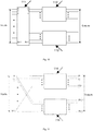
FIG. 2 is a schematic block diagram showing a recursive construction of the concentrator circuit ofFIG. 1 ; -
FIG. 3 is a schematic block diagram of a concentrator according toFIG. 2 with its two configuration modules and a column of switches; -
FIG. 4 shows an electrical circuit for computing the activity bits in the leftmost module ofFIG. 3 according to one embodiment of the invention; -
FIG. 5 is a schematic block diagram showing one embodiment of a second module ofFIG. 3 according to the invention for computing parity bits; -
FIG. 6 is a schematic block diagram showing a first stage of parity bits computation done in the second module according toFIG. 5 ; -
FIG. 7 is a gate level diagram for computing the parallel prefix sum for n=16 inputs; -
FIG. 8 is a circuit diagram of a complete concentrator for eight inputs according to one embodiment of the invention; -
FIG. 9 is a schematic block diagram of a selector module according to one embodiment of the present invention; -
FIG. 10 shows one embodiment of a recursive construction of the selector-tree interconnection network according to the present invention; -
FIG. 11 is a schematic block diagram of a node of the selector-tree ofFIG. 10 ; and -
FIG. 12 is a schematic block diagram of a 8 inputs selector-tree network constructed from the selector module according toFIG. 10 . - The various embodiments will be described in detail with reference to the accompanying drawings. Wherever possible, the same reference numbers will be used throughout the drawings to refer to the same or like parts. References made to particular examples and implementations are for illustrative purposes, and are not intended to limit the scope of the invention or the claims.
- As shown in
FIG. 1 , the concentrator according to this exemplarily embodiment of the present invention is an n×n network. Its function is to route all the active inputs to the bottom end of the network's outputs. Each input x[i] comprises data bits data(x[i]) and a single valid bit valid(x[i]) such that the valid bit indicates whether the input is valid. The data bits comprise a message msg(x[i]) and a target address tgt(x[i]). Moreover, the concentrator can be either positive or negative which differs in the definition of active inputs: To this end, the most significant bit (msb) of the target address is considered. Input x[i] is considered active by the positive concentrator if valid(x[i]) & msb(tgt(x[i])) holds, while a negative concentrator considers x[i] active if valid(x[i]) & not(msb(tgt(x[i]))) holds. As shown inFIG. 1 , the concentrator consists of a butterfly permutation (module 108) and amodule 101 which is the main part of the concentrator that routes the active inputs to known outputs (andmodel 108 permutes these to the bottom end of the network's outputs). - A
module 101 for n inputs/outputs can be constructed by twomodules 101 with n/2 inputs/outputs and one module numbered as 102 as shown inFIG. 2 . The outputs of themodule 102 and the inputs of the twomodules 101 are interleaved by the flip shuffle permutation (module 107).Module 102 comprises a column of n/2 2×2 crossbar switches and the control logic for configuring these crossbar switches. The control logic has to configure the switches such that half of the active inputs is routed to one of the twomodules 101 and the other half is routed to theother module 101. If there is an odd number of active inputs, thelower module 101 gets one more active input than the other one. By decomposing each one of themodules 101 recursively, a network consisting of log2(n) stages of 2×2 crossbar switches and their control logic for configuring the crossbar switches is obtained. - A configuration module of
type 102 shown exemplarily inFIG. 2 comprises crossbar switches and the control logic to configure these switches as shown inFIG. 3 . As can be seen inFIG. 3 , aconfiguration module 102 is decomposed into three modules, afirst module 104, asecond module 105 and athird module 106 that are arranged in a sequence to build one module oftype 102. The first and the second module 104,105 implement thereby the control logic for the switches that are comprised by thethird module 106. - One possible implementation of the
first module 104 is given by a column of n circuits as shown inFIG. 4 . The purpose of thisfirst module 104 is to determine which inputs are active ones. As explained above, the activity bit is computed as valid(x[i]) & XNOR(msb(tgt(x[i])),p) where p is true/false for positive/negative concentrators, respectively. For n inputs, therefore n of the circuits shown inFIG. 4 in n column are arranged to implement thefirst module 104. - Having computed the activity bits of every input, the next task is to configure the switches contained in the
third module 106 ofFIG. 3 . To this end, we have to compute for all even numbers i, the parity bits as p[i] := x[0] ⊕ ... ⊕ x[i] for the activity bits x[i]. To compute these bits in parallel, we compute the prefixes of all activity bits with the XOR operation, which can be done for all n inputs with O(log2(n)) time steps and O(n) gates. These prefixes are then used to configure the switches ofmodule 106 in parallel. - The computation of all even indexed prefixes p[i] can be done according to one embodiment by two stages as shown in
FIG. 5 : The first stage, denoted asmodule 109 contains n/2 XOR gates to compute the parity of inputs 2i-1 and 2i as shown inFIG. 6 . In this diagram, x[2i-1] and x[2i] denote the activity bits that are the inputs of the i-th row while y[i] denotes the output of the i-th row for i=1,...,n/2-1. Note that for i = 0, the output is same as the input, i.e., y[0] := x[0]. -
Module 110 therefore receives the n/2 outputs y[i] as computed bymodule 109 and computes the parities of their prefixes, i.e. p[i] := y[0] ⊕ ... ⊕ y[i] = x[0] ⊕ ... ⊕ x[2i] for the activity bits x[i]. This is done by a work-efficient parallel prefix sum as described in G.E. Blelloch, "Prefix Sums and Their Applications", a chapter of "Synthesis of Parallel Algorithms" edited by J.H. Reif, pp. 35-60, Morgan Kaufmann, 1990 which is shown for n=16 inputs inFIG. 7 . The output of the parallel prefix sum configures the 2×2 crossbar switches inmodule 106. - The complete embodiment of a concentrator according to the invention for eight inputs is shown in
FIG. 8 without the butterfly permutation (module 108). It has O(log2(n)) switching stages and O(log2(n)) control logic stages and requires O(n·log2(n)) gates in total. -
FIG. 9 shows one embodiment of a selector module which is a (n,n/2)-concentrator. A selector module can serve as a building block in constructing a selector-tree interconnection network. This interconnection network is capable of routing any permutation of its n inputs to its n outputs and is therefore non-blocking. - The topology of the selector-tree network according to this embodiment follows a fat tree structure as shown in
FIG. 10 , where each node of the fat tree with n inputs has 2 children. The task of the root node is to split the given n inputs into 2 partitions according to their most significant bit of the target addresses so that these can be recursively routed by 2 subnetworks (shown asmodules 112 inFIG. 10 ) each one having n/2 inputs/outputs. - While assuming that there is no routing conflict in the sense that no input messages i and j should be routed at the same time to the same target address, i.e., denoting the target address of input i as tgt(x[i]), it is assumed that for all i≠j that tgt(x[i])≠ tgt(x[j]) holds. The selector-tree network is capable of implementing every permutation without any difficult setup algorithm as required for other networks.
- As can be seen in
FIG. 11 , the nodes of the selector-tree network with n inputs consist of twoselector modules 114 both having n inputs and n/2 outputs. The upper module is a negative (n,n/2)-concentrator and the lower module is a positive (n,n/2)-concentrator. All inputs are forwarded to both the positive and the negative concentrator modules that consider then the inputs with positive or negative most significant bit of the target address as being active, and will select them for routing to one of its outputs. - By further decomposing each one of the (n/2)-input selector-tree networks shown as
modules 112 inFIG. 10 recursively for eight inputs, we obtain a network consisting of 3 stages as shown inFIG. 12 . We can prove that for n inputs, this network requires O(log2(n)3) time and O(n•log2(n)2) gates and can moreover work in a pipelined mode.
Claims (8)
- A concentrator for a nonblocking interconnection network comprising a plurality of n global inputs and a plurality of n global outputs for processing m active inputs to m outputs, wherein m ≤ n, and wherein each input x[i] includes data bits data(x[i]) and a single valid bit valid(x[i]), wherein the concentrator comprises log2(n) columns with n/2 rows of 2×2 crossbar switches, wherein the crossbar switches of each of the log2(n) columns are connected with corresponding crossbar switches of the next column starting from the n global inputs to the n global outputs, wherein a configuration module for configuring the crossbar switches is comprised, wherein the configuration module comprises the first column of n/2 rows of the 2×2 crossbar switches of the concentrator, each input of said crossbar switches is connected to one of the n global inputs and the outputs of said crossbar switches are interleavingly connected by a flip shuffle permutation to the inputs of two internal concentrators with n/2 internal inputs and n/2 internal outputs, wherein said n/2 internal outputs are interleavingly connected to the n global outputs by a butterfly permutation, wherein the configuration of the crossbar switches belonging to a given column is based on the parity of the number of valid inputs of the respective column and wherein the parity of the number of valid inputs of all the columns are computed in parallel, and wherein the parity of the number of valid inputs of a column defines whether the number of valid inputs x[0..i] of said column is even or odd at position i, characterized in that
the configuration module yields a binary tree of base modules and the base modules comprise three modules arranged in a sequence, wherein the first and the second module of said three modules comprises the control logic for the crossbar switches of the configuration module and the third module of said three modules comprises said crossbar switches , and wherein the first module comprises n elements arranged in a row, each of said elements being connected to a global input, wherein each of these elements is configured and adapted to determine whether an input x[i] is considered to be active and wherein the second module is configured and adapted to compute for all even numbers i parity bits as p[i] := x[0] ⊕ ... ⊕ x[i] for activity bits x[i], where ⊕ denotes the exclusive-or operation. - A concentrator according to claim 1, wherein
the n/2 2×2 crossbar switches are configured such that half of the active n global inputs is routed to each one of the two internal concentrators, wherein in case of an odd number of active inputs, the lower concentrator gets one more active inputs than the other one. - A concentrator according to the preceding claims, wherein
the data bits comprises a message msg(x[i]) and a target address tgt(x[i]), wherein the most significant bit, msb, of the target address is considered by the concentratorwhen determining whether an input x[i] is considered to be active. - A concentrator according to claim 1, wherein
in case of a positive concentrator an input x[i] is considered to be active if valid(x[i]) & msb(tgt(x[i])) or in case of a negative concentrator an input x[i] is considered to be active if valid(x[i]) & not(msb(tgt(x[i]))), wherein msb indentifies the most significant bit and valid identifies whether the input is active. - A concentrator according to any of the preceding claims, wherein
the second module is configured and adapted to execute a parallel prefix tree computation in 2 log2(n)-1 time steps using 2n - log2(n) - 1 XOR gates to compute said parity bits. - A concentrator according any of the preceding claims, wherein
the second module comprises two sub-modules wherein the first sub-module comprises n/2 XOR gates and is configured and adapted to compute the parity of inputs x[2i-1] and x[2i] providing y[i] outputs as inputs for the second sub-module, the second sub-module being configured and adapted to compute the parities of their prefixes p[i] := y[0] ⊕ ... ⊕ y[i] = x[0] ⊕ ... ⊕ x[2i] for the activity bits x[i], where ⊕ denotes the exclusive-or operation with a parallel prefix sum network. - A concentrator according to claim 6, wherein
the prefixes of the parallel prefix sum of the parity bits is used to configure the crossbar switches of the third module in parallel. - Use of a concentrator according to any one of the preceding claims as a building block of an interconnection network.
Priority Applications (1)
| Application Number | Priority Date | Filing Date | Title |
|---|---|---|---|
| EP16202555.5A EP3334106B1 (en) | 2016-12-06 | 2016-12-06 | A recursive concentrator circuit and its application as building block of an interconnection network |
Applications Claiming Priority (1)
| Application Number | Priority Date | Filing Date | Title |
|---|---|---|---|
| EP16202555.5A EP3334106B1 (en) | 2016-12-06 | 2016-12-06 | A recursive concentrator circuit and its application as building block of an interconnection network |
Publications (2)
| Publication Number | Publication Date |
|---|---|
| EP3334106A1 EP3334106A1 (en) | 2018-06-13 |
| EP3334106B1 true EP3334106B1 (en) | 2021-07-28 |
Family
ID=57544233
Family Applications (1)
| Application Number | Title | Priority Date | Filing Date |
|---|---|---|---|
| EP16202555.5A Active EP3334106B1 (en) | 2016-12-06 | 2016-12-06 | A recursive concentrator circuit and its application as building block of an interconnection network |
Country Status (1)
| Country | Link |
|---|---|
| EP (1) | EP3334106B1 (en) |
Families Citing this family (1)
| Publication number | Priority date | Publication date | Assignee | Title |
|---|---|---|---|---|
| CN115102914A (en) * | 2021-03-05 | 2022-09-23 | 中兴通讯股份有限公司 | Data exchange system, method and storage medium |
-
2016
- 2016-12-06 EP EP16202555.5A patent/EP3334106B1/en active Active
Non-Patent Citations (1)
| Title |
|---|
| None * |
Also Published As
| Publication number | Publication date |
|---|---|
| EP3334106A1 (en) | 2018-06-13 |
Similar Documents
| Publication | Publication Date | Title |
|---|---|---|
| Narasimha | The Batcher-Banyan self-routing network: universality and simplification | |
| Finkel | Processor interconnection strategies | |
| US7457303B2 (en) | One-bounce network | |
| Jan et al. | Fast self-routing permutation switching on an asymptotically minimum cost network | |
| EP3334106A1 (en) | A recursive concentrator circuit and its application as building block of an interconnection network | |
| Yuan | On nonblocking folded-clos networks in computer communication environments | |
| Quinton et al. | Concentrator access networks for programmable logic cores on SoCs | |
| Brahme et al. | SymSig: A low latency interconnection topology for HPC clusters | |
| Narasimha | A recursive concentrator structure with applications to self-routing switching networks | |
| Jain et al. | An efficient self-routing and non-blocking interconnection network on chip | |
| Jain et al. | Routing partial permutations in interconnection networks based on radix sorting | |
| Jain et al. | Verifying the concentration property of permutation networks by BDDs | |
| Koloko et al. | Design and implementation of fast and hardware‐efficient parallel processing elements to set full and partial permutations in Beneš networks | |
| Jain et al. | Deriving concentrators from binary sorters using half cleaners | |
| US5034946A (en) | Broadband concentrator for packet switch | |
| Jain et al. | Routing Partial Permutations in General Interconnection Networks based on Radix Sorting. | |
| Jain et al. | The half cleaner lemma: Constructing efficient interconnection networks from sorting networks | |
| Sharma et al. | Performance analysis of high speed low-latency torus optical network | |
| Lysaght et al. | Of gates and wires | |
| Koloko | A study on improving the performance of three-stage Clos networks | |
| Jain et al. | The selector-tree network: A new self-routing and non-blocking interconnection network | |
| Oruç | One-sided binary tree-crossbar switching for on-chip networks | |
| Hung et al. | Embedding two edge-disjoint Hamiltonian cycles and two equal node-disjoint cycles into twisted cubes | |
| Jain et al. | Optimal self-routing split modules for radix-based interconnection networks | |
| Lil et al. | Fault Tolerance and Packet Latency |
Legal Events
| Date | Code | Title | Description |
|---|---|---|---|
| PUAI | Public reference made under article 153(3) epc to a published international application that has entered the european phase |
Free format text: ORIGINAL CODE: 0009012 |
|
| STAA | Information on the status of an ep patent application or granted ep patent |
Free format text: STATUS: THE APPLICATION HAS BEEN PUBLISHED |
|
| AK | Designated contracting states |
Kind code of ref document: A1 Designated state(s): AL AT BE BG CH CY CZ DE DK EE ES FI FR GB GR HR HU IE IS IT LI LT LU LV MC MK MT NL NO PL PT RO RS SE SI SK SM TR |
|
| AX | Request for extension of the european patent |
Extension state: BA ME |
|
| STAA | Information on the status of an ep patent application or granted ep patent |
Free format text: STATUS: REQUEST FOR EXAMINATION WAS MADE |
|
| 17P | Request for examination filed |
Effective date: 20181213 |
|
| RBV | Designated contracting states (corrected) |
Designated state(s): AL AT BE BG CH CY CZ DE DK EE ES FI FR GB GR HR HU IE IS IT LI LT LU LV MC MK MT NL NO PL PT RO RS SE SI SK SM TR |
|
| STAA | Information on the status of an ep patent application or granted ep patent |
Free format text: STATUS: EXAMINATION IS IN PROGRESS |
|
| 17Q | First examination report despatched |
Effective date: 20190401 |
|
| GRAP | Despatch of communication of intention to grant a patent |
Free format text: ORIGINAL CODE: EPIDOSNIGR1 |
|
| STAA | Information on the status of an ep patent application or granted ep patent |
Free format text: STATUS: GRANT OF PATENT IS INTENDED |
|
| INTG | Intention to grant announced |
Effective date: 20210222 |
|
| GRAS | Grant fee paid |
Free format text: ORIGINAL CODE: EPIDOSNIGR3 |
|
| GRAA | (expected) grant |
Free format text: ORIGINAL CODE: 0009210 |
|
| STAA | Information on the status of an ep patent application or granted ep patent |
Free format text: STATUS: THE PATENT HAS BEEN GRANTED |
|
| AK | Designated contracting states |
Kind code of ref document: B1 Designated state(s): AL AT BE BG CH CY CZ DE DK EE ES FI FR GB GR HR HU IE IS IT LI LT LU LV MC MK MT NL NO PL PT RO RS SE SI SK SM TR |
|
| REG | Reference to a national code |
Ref country code: GB Ref legal event code: FG4D |
|
| REG | Reference to a national code |
Ref country code: CH Ref legal event code: EP |
|
| REG | Reference to a national code |
Ref country code: DE Ref legal event code: R096 Ref document number: 602016061205 Country of ref document: DE |
|
| REG | Reference to a national code |
Ref country code: AT Ref legal event code: REF Ref document number: 1415747 Country of ref document: AT Kind code of ref document: T Effective date: 20210815 |
|
| REG | Reference to a national code |
Ref country code: IE Ref legal event code: FG4D |
|
| REG | Reference to a national code |
Ref country code: LT Ref legal event code: MG9D |
|
| REG | Reference to a national code |
Ref country code: DE Ref legal event code: R079 Ref document number: 602016061205 Country of ref document: DE Free format text: PREVIOUS MAIN CLASS: H04L0012933000 Ipc: H04L0049100000 |
|
| REG | Reference to a national code |
Ref country code: NL Ref legal event code: MP Effective date: 20210728 |
|
| REG | Reference to a national code |
Ref country code: AT Ref legal event code: MK05 Ref document number: 1415747 Country of ref document: AT Kind code of ref document: T Effective date: 20210728 |
|
| PG25 | Lapsed in a contracting state [announced via postgrant information from national office to epo] |
Ref country code: HR Free format text: LAPSE BECAUSE OF FAILURE TO SUBMIT A TRANSLATION OF THE DESCRIPTION OR TO PAY THE FEE WITHIN THE PRESCRIBED TIME-LIMIT Effective date: 20210728 Ref country code: SE Free format text: LAPSE BECAUSE OF FAILURE TO SUBMIT A TRANSLATION OF THE DESCRIPTION OR TO PAY THE FEE WITHIN THE PRESCRIBED TIME-LIMIT Effective date: 20210728 Ref country code: RS Free format text: LAPSE BECAUSE OF FAILURE TO SUBMIT A TRANSLATION OF THE DESCRIPTION OR TO PAY THE FEE WITHIN THE PRESCRIBED TIME-LIMIT Effective date: 20210728 Ref country code: LT Free format text: LAPSE BECAUSE OF FAILURE TO SUBMIT A TRANSLATION OF THE DESCRIPTION OR TO PAY THE FEE WITHIN THE PRESCRIBED TIME-LIMIT Effective date: 20210728 Ref country code: AT Free format text: LAPSE BECAUSE OF FAILURE TO SUBMIT A TRANSLATION OF THE DESCRIPTION OR TO PAY THE FEE WITHIN THE PRESCRIBED TIME-LIMIT Effective date: 20210728 Ref country code: BG Free format text: LAPSE BECAUSE OF FAILURE TO SUBMIT A TRANSLATION OF THE DESCRIPTION OR TO PAY THE FEE WITHIN THE PRESCRIBED TIME-LIMIT Effective date: 20211028 Ref country code: FI Free format text: LAPSE BECAUSE OF FAILURE TO SUBMIT A TRANSLATION OF THE DESCRIPTION OR TO PAY THE FEE WITHIN THE PRESCRIBED TIME-LIMIT Effective date: 20210728 Ref country code: ES Free format text: LAPSE BECAUSE OF FAILURE TO SUBMIT A TRANSLATION OF THE DESCRIPTION OR TO PAY THE FEE WITHIN THE PRESCRIBED TIME-LIMIT Effective date: 20210728 Ref country code: NL Free format text: LAPSE BECAUSE OF FAILURE TO SUBMIT A TRANSLATION OF THE DESCRIPTION OR TO PAY THE FEE WITHIN THE PRESCRIBED TIME-LIMIT Effective date: 20210728 Ref country code: NO Free format text: LAPSE BECAUSE OF FAILURE TO SUBMIT A TRANSLATION OF THE DESCRIPTION OR TO PAY THE FEE WITHIN THE PRESCRIBED TIME-LIMIT Effective date: 20211028 Ref country code: PT Free format text: LAPSE BECAUSE OF FAILURE TO SUBMIT A TRANSLATION OF THE DESCRIPTION OR TO PAY THE FEE WITHIN THE PRESCRIBED TIME-LIMIT Effective date: 20211129 |
|
| PG25 | Lapsed in a contracting state [announced via postgrant information from national office to epo] |
Ref country code: PL Free format text: LAPSE BECAUSE OF FAILURE TO SUBMIT A TRANSLATION OF THE DESCRIPTION OR TO PAY THE FEE WITHIN THE PRESCRIBED TIME-LIMIT Effective date: 20210728 Ref country code: LV Free format text: LAPSE BECAUSE OF FAILURE TO SUBMIT A TRANSLATION OF THE DESCRIPTION OR TO PAY THE FEE WITHIN THE PRESCRIBED TIME-LIMIT Effective date: 20210728 Ref country code: GR Free format text: LAPSE BECAUSE OF FAILURE TO SUBMIT A TRANSLATION OF THE DESCRIPTION OR TO PAY THE FEE WITHIN THE PRESCRIBED TIME-LIMIT Effective date: 20211029 |
|
| PG25 | Lapsed in a contracting state [announced via postgrant information from national office to epo] |
Ref country code: DK Free format text: LAPSE BECAUSE OF FAILURE TO SUBMIT A TRANSLATION OF THE DESCRIPTION OR TO PAY THE FEE WITHIN THE PRESCRIBED TIME-LIMIT Effective date: 20210728 |
|
| REG | Reference to a national code |
Ref country code: DE Ref legal event code: R097 Ref document number: 602016061205 Country of ref document: DE |
|
| PG25 | Lapsed in a contracting state [announced via postgrant information from national office to epo] |
Ref country code: SM Free format text: LAPSE BECAUSE OF FAILURE TO SUBMIT A TRANSLATION OF THE DESCRIPTION OR TO PAY THE FEE WITHIN THE PRESCRIBED TIME-LIMIT Effective date: 20210728 Ref country code: SK Free format text: LAPSE BECAUSE OF FAILURE TO SUBMIT A TRANSLATION OF THE DESCRIPTION OR TO PAY THE FEE WITHIN THE PRESCRIBED TIME-LIMIT Effective date: 20210728 Ref country code: RO Free format text: LAPSE BECAUSE OF FAILURE TO SUBMIT A TRANSLATION OF THE DESCRIPTION OR TO PAY THE FEE WITHIN THE PRESCRIBED TIME-LIMIT Effective date: 20210728 Ref country code: EE Free format text: LAPSE BECAUSE OF FAILURE TO SUBMIT A TRANSLATION OF THE DESCRIPTION OR TO PAY THE FEE WITHIN THE PRESCRIBED TIME-LIMIT Effective date: 20210728 Ref country code: CZ Free format text: LAPSE BECAUSE OF FAILURE TO SUBMIT A TRANSLATION OF THE DESCRIPTION OR TO PAY THE FEE WITHIN THE PRESCRIBED TIME-LIMIT Effective date: 20210728 Ref country code: AL Free format text: LAPSE BECAUSE OF FAILURE TO SUBMIT A TRANSLATION OF THE DESCRIPTION OR TO PAY THE FEE WITHIN THE PRESCRIBED TIME-LIMIT Effective date: 20210728 |
|
| PLBE | No opposition filed within time limit |
Free format text: ORIGINAL CODE: 0009261 |
|
| STAA | Information on the status of an ep patent application or granted ep patent |
Free format text: STATUS: NO OPPOSITION FILED WITHIN TIME LIMIT |
|
| 26N | No opposition filed |
Effective date: 20220429 |
|
| PG25 | Lapsed in a contracting state [announced via postgrant information from national office to epo] |
Ref country code: MC Free format text: LAPSE BECAUSE OF FAILURE TO SUBMIT A TRANSLATION OF THE DESCRIPTION OR TO PAY THE FEE WITHIN THE PRESCRIBED TIME-LIMIT Effective date: 20210728 Ref country code: IT Free format text: LAPSE BECAUSE OF FAILURE TO SUBMIT A TRANSLATION OF THE DESCRIPTION OR TO PAY THE FEE WITHIN THE PRESCRIBED TIME-LIMIT Effective date: 20210728 |
|
| REG | Reference to a national code |
Ref country code: CH Ref legal event code: PL |
|
| REG | Reference to a national code |
Ref country code: BE Ref legal event code: MM Effective date: 20211231 |
|
| PG25 | Lapsed in a contracting state [announced via postgrant information from national office to epo] |
Ref country code: LU Free format text: LAPSE BECAUSE OF NON-PAYMENT OF DUE FEES Effective date: 20211206 Ref country code: IE Free format text: LAPSE BECAUSE OF NON-PAYMENT OF DUE FEES Effective date: 20211206 |
|
| PG25 | Lapsed in a contracting state [announced via postgrant information from national office to epo] |
Ref country code: BE Free format text: LAPSE BECAUSE OF NON-PAYMENT OF DUE FEES Effective date: 20211231 |
|
| PG25 | Lapsed in a contracting state [announced via postgrant information from national office to epo] |
Ref country code: LI Free format text: LAPSE BECAUSE OF NON-PAYMENT OF DUE FEES Effective date: 20211231 Ref country code: CH Free format text: LAPSE BECAUSE OF NON-PAYMENT OF DUE FEES Effective date: 20211231 |
|
| PG25 | Lapsed in a contracting state [announced via postgrant information from national office to epo] |
Ref country code: HU Free format text: LAPSE BECAUSE OF FAILURE TO SUBMIT A TRANSLATION OF THE DESCRIPTION OR TO PAY THE FEE WITHIN THE PRESCRIBED TIME-LIMIT; INVALID AB INITIO Effective date: 20161206 |
|
| PG25 | Lapsed in a contracting state [announced via postgrant information from national office to epo] |
Ref country code: CY Free format text: LAPSE BECAUSE OF FAILURE TO SUBMIT A TRANSLATION OF THE DESCRIPTION OR TO PAY THE FEE WITHIN THE PRESCRIBED TIME-LIMIT Effective date: 20210728 |
|
| PGFP | Annual fee paid to national office [announced via postgrant information from national office to epo] |
Ref country code: GB Payment date: 20231220 Year of fee payment: 8 |
|
| PGFP | Annual fee paid to national office [announced via postgrant information from national office to epo] |
Ref country code: FR Payment date: 20231220 Year of fee payment: 8 |
|
| PG25 | Lapsed in a contracting state [announced via postgrant information from national office to epo] |
Ref country code: MK Free format text: LAPSE BECAUSE OF FAILURE TO SUBMIT A TRANSLATION OF THE DESCRIPTION OR TO PAY THE FEE WITHIN THE PRESCRIBED TIME-LIMIT Effective date: 20210728 |
|
| PGFP | Annual fee paid to national office [announced via postgrant information from national office to epo] |
Ref country code: DE Payment date: 20231219 Year of fee payment: 8 |
|
| PG25 | Lapsed in a contracting state [announced via postgrant information from national office to epo] |
Ref country code: MT Free format text: LAPSE BECAUSE OF FAILURE TO SUBMIT A TRANSLATION OF THE DESCRIPTION OR TO PAY THE FEE WITHIN THE PRESCRIBED TIME-LIMIT Effective date: 20210728 |
|
| REG | Reference to a national code |
Ref country code: DE Ref legal event code: R119 Ref document number: 602016061205 Country of ref document: DE |
|
| GBPC | Gb: european patent ceased through non-payment of renewal fee |
Effective date: 20241206 |
|
| PG25 | Lapsed in a contracting state [announced via postgrant information from national office to epo] |
Ref country code: DE Free format text: LAPSE BECAUSE OF NON-PAYMENT OF DUE FEES Effective date: 20250701 |
|
| PG25 | Lapsed in a contracting state [announced via postgrant information from national office to epo] |
Ref country code: GB Free format text: LAPSE BECAUSE OF NON-PAYMENT OF DUE FEES Effective date: 20241206 |
|
| PG25 | Lapsed in a contracting state [announced via postgrant information from national office to epo] |
Ref country code: FR Free format text: LAPSE BECAUSE OF NON-PAYMENT OF DUE FEES Effective date: 20241231 |
|
| PG25 | Lapsed in a contracting state [announced via postgrant information from national office to epo] |
Ref country code: TR Free format text: LAPSE BECAUSE OF FAILURE TO SUBMIT A TRANSLATION OF THE DESCRIPTION OR TO PAY THE FEE WITHIN THE PRESCRIBED TIME-LIMIT Effective date: 20210728 |