EP3334039A1 - Source follower - Google Patents
Source follower Download PDFInfo
- Publication number
- EP3334039A1 EP3334039A1 EP17205766.3A EP17205766A EP3334039A1 EP 3334039 A1 EP3334039 A1 EP 3334039A1 EP 17205766 A EP17205766 A EP 17205766A EP 3334039 A1 EP3334039 A1 EP 3334039A1
- Authority
- EP
- European Patent Office
- Prior art keywords
- transistor
- source follower
- voltage
- node
- coupled
- Prior art date
- Legal status (The legal status is an assumption and is not a legal conclusion. Google has not performed a legal analysis and makes no representation as to the accuracy of the status listed.)
- Granted
Links
Images




Classifications
-
- H—ELECTRICITY
- H03—ELECTRONIC CIRCUITRY
- H03K—PULSE TECHNIQUE
- H03K19/00—Logic circuits, i.e. having at least two inputs acting on one output; Inverting circuits
- H03K19/003—Modifications for increasing the reliability for protection
- H03K19/00315—Modifications for increasing the reliability for protection in field-effect transistor circuits
-
- H—ELECTRICITY
- H03—ELECTRONIC CIRCUITRY
- H03F—AMPLIFIERS
- H03F1/00—Details of amplifiers with only discharge tubes, only semiconductor devices or only unspecified devices as amplifying elements
- H03F1/32—Modifications of amplifiers to reduce non-linear distortion
- H03F1/3205—Modifications of amplifiers to reduce non-linear distortion in field-effect transistor amplifiers
-
- H—ELECTRICITY
- H03—ELECTRONIC CIRCUITRY
- H03F—AMPLIFIERS
- H03F1/00—Details of amplifiers with only discharge tubes, only semiconductor devices or only unspecified devices as amplifying elements
- H03F1/02—Modifications of amplifiers to raise the efficiency, e.g. gliding Class A stages, use of an auxiliary oscillation
- H03F1/0205—Modifications of amplifiers to raise the efficiency, e.g. gliding Class A stages, use of an auxiliary oscillation in transistor amplifiers
- H03F1/0211—Modifications of amplifiers to raise the efficiency, e.g. gliding Class A stages, use of an auxiliary oscillation in transistor amplifiers with control of the supply voltage or current
- H03F1/0216—Continuous control
- H03F1/0233—Continuous control by using a signal derived from the output signal, e.g. bootstrapping the voltage supply
-
- H—ELECTRICITY
- H03—ELECTRONIC CIRCUITRY
- H03F—AMPLIFIERS
- H03F1/00—Details of amplifiers with only discharge tubes, only semiconductor devices or only unspecified devices as amplifying elements
- H03F1/02—Modifications of amplifiers to raise the efficiency, e.g. gliding Class A stages, use of an auxiliary oscillation
- H03F1/0205—Modifications of amplifiers to raise the efficiency, e.g. gliding Class A stages, use of an auxiliary oscillation in transistor amplifiers
- H03F1/0211—Modifications of amplifiers to raise the efficiency, e.g. gliding Class A stages, use of an auxiliary oscillation in transistor amplifiers with control of the supply voltage or current
- H03F1/0244—Stepped control
- H03F1/0255—Stepped control by using a signal derived from the output signal
-
- H—ELECTRICITY
- H03—ELECTRONIC CIRCUITRY
- H03F—AMPLIFIERS
- H03F3/00—Amplifiers with only discharge tubes or only semiconductor devices as amplifying elements
- H03F3/189—High-frequency amplifiers, e.g. radio frequency amplifiers
- H03F3/19—High-frequency amplifiers, e.g. radio frequency amplifiers with semiconductor devices only
- H03F3/193—High-frequency amplifiers, e.g. radio frequency amplifiers with semiconductor devices only with field-effect devices
-
- H—ELECTRICITY
- H03—ELECTRONIC CIRCUITRY
- H03F—AMPLIFIERS
- H03F3/00—Amplifiers with only discharge tubes or only semiconductor devices as amplifying elements
- H03F3/34—DC amplifiers in which all stages are DC-coupled
- H03F3/343—DC amplifiers in which all stages are DC-coupled with semiconductor devices only
- H03F3/345—DC amplifiers in which all stages are DC-coupled with semiconductor devices only with field-effect devices
-
- H—ELECTRICITY
- H03—ELECTRONIC CIRCUITRY
- H03K—PULSE TECHNIQUE
- H03K19/00—Logic circuits, i.e. having at least two inputs acting on one output; Inverting circuits
- H03K19/0175—Coupling arrangements; Interface arrangements
- H03K19/0185—Coupling arrangements; Interface arrangements using field effect transistors only
- H03K19/018507—Interface arrangements
-
- H—ELECTRICITY
- H03—ELECTRONIC CIRCUITRY
- H03F—AMPLIFIERS
- H03F2200/00—Indexing scheme relating to amplifiers
- H03F2200/102—A non-specified detector of a signal envelope being used in an amplifying circuit
-
- H—ELECTRICITY
- H03—ELECTRONIC CIRCUITRY
- H03F—AMPLIFIERS
- H03F2200/00—Indexing scheme relating to amplifiers
- H03F2200/66—Clipping circuitry being present in an amplifier, i.e. the shape of the signal being modified
-
- H—ELECTRICITY
- H03—ELECTRONIC CIRCUITRY
- H03F—AMPLIFIERS
- H03F2200/00—Indexing scheme relating to amplifiers
- H03F2200/69—Indexing scheme relating to amplifiers the amplifier stage being a common drain coupled MOSFET, i.e. source follower
Definitions
- the disclosure generally relates to a source follower, and more specifically, to a source follower for suppressing second harmonic distortion.
- a single-input-ended source follower is very sensitive to PVT (Process, Voltage, and Temperature) variations, which are the result of second harmonic distortion relative to the source follower.
- PVT Process, Voltage, and Temperature
- the second harmonic distortion becomes worse when the variations of drain-to-source voltage of the input transistor and the current source are not symmetry to output-common mode voltage. Serious second harmonic distortion may degrade the linearity of the source follower, thereby negatively affecting its performance. Accordingly, there is a need to propose a novel solution to the problems with the prior art.
- the disclosure is directed to a source follower with an input node and an output node
- the source follower includes a first transistor, a second transistor, and a DC (Direct Current) tracking circuit.
- the first transistor has a control terminal, a first terminal coupled to a first node, and a second terminal coupled to a second node.
- the second transistor has a control terminal, a first terminal coupled to a ground voltage, and a second terminal coupled to the first node.
- the DC tracking circuit sets a second DC voltage at the second node to a specific level. The specific level is determined according to a first DC voltage at the first node.
- the output node of the source follower is coupled to the first node.
- the second DC voltage is substantially equal to two times the first DC voltage.
- the DC tracking circuit is implemented with an open-loop operational amplifier, a closed-loop operational amplifier, or a linear regulator.
- the input node of the source follower is coupled to the control terminal of the first transistor, and a bias voltage is coupled to the control terminal of the second transistor.
- the first transistor and the second transistor are NMOS transistors (N-type Metal-Oxide-Semiconductor Field-Effect Transistors).
- the DC tracking circuit includes a first operational amplifier, a third transistor, a fourth transistor, a first resistor, a second resistor, and a second operational amplifier.
- the first operational amplifier has a positive input terminal for receiving a first DC reference voltage, a negative input terminal coupled to a third node, and an output terminal coupled to a fourth node.
- the third transistor has a control terminal coupled to the fourth node, a first terminal coupled to a fifth node, and a second terminal coupled to a supply voltage.
- the fourth transistor has a control terminal coupled to the fourth node, a first terminal coupled to the second node, and a second terminal coupled to the supply voltage.
- the first resistor is coupled between the fifth node and the third node.
- the second resistor is coupled between the third node and the ground voltage.
- the second operational amplifier has a positive input terminal for receiving the first DC reference voltage, a negative input terminal for receiving a second DC reference voltage, and an output terminal coupled to the input node of the source follower.
- both the first DC voltage and the second DC reference voltage are equal to the first DC reference voltage.
- the third transistor and the fourth transistor are NMOS transistors (N-type Metal-Oxide-Semiconductor Field-Effect Transistors).
- a DC component of an output voltage at the output node of the source follower is fed back to the second DC reference voltage.
- the input node of the source follower is coupled to the control terminal of the second transistor, and a bias voltage is coupled to the control terminal of the first transistor.
- the first transistor and the second transistor are PMOS transistors (P-type Metal-Oxide-Semiconductor Field-Effect Transistors).
- the invention is directed to a source follower with an input node and an output node
- the source follower includes a first transistor, a second transistor, and a DC (Direct Current) tracking circuit.
- the first transistor has a control terminal, a first terminal coupled to a first node, and a second terminal coupled to a supply voltage.
- the second transistor has a control terminal, a first terminal coupled to a second node, and a second terminal coupled to the first node.
- the DC tracking circuit sets the second DC voltage at the second node to a specific level. The specific level is determined according to the first DC voltage at the first node.
- the output node of the source follower is coupled to the first node.
- the second DC voltage is substantially equal to two times the first DC voltage minus the supply voltage.
- FIG. 1 is a diagram of a source follower 100 according to an embodiment of the invention.
- the source follower 100 with an input node NIN and an output node NOUT includes a first transistor M1, a second transistor M2, and a DC (Direct Current) tracking circuit 110.
- the input node NIN of the source follower 100 is arranged for receiving an input voltage VIN
- the output node NOUT of the source follower 100 is arranged for outputting an output voltage VOUT.
- the waveform of the output voltage VOUT substantially follows the waveform of the input voltage VIN.
- the first transistor M1 and the second transistor M2 are NMOS transistors (N-type Metal-Oxide-Semiconductor Field-Effect Transistors).
- the first transistor M1 and the second transistor M2 may have the same transistor sizes.
- the first transistor M1 has a control terminal, a first terminal coupled to a first node N1, and a second terminal coupled to a second node N2.
- the input node NIN of the source follower 100 is coupled to the control terminal of the first transistor M1, and the output node NOUT of the source follower 100 is coupled to the first node N1, such that the first transistor M1 is used as an input transistor.
- the second transistor M2 has a control terminal, a first terminal coupled to a ground voltage VSS, and a second terminal coupled to the first node N1.
- a bias voltage VB is coupled to the control terminal of the second transistor M2, such that the second transistor M2 is used as a current source.
- the DC tracking circuit 110 sets a second DC voltage VD2 at the second node N2 to a specific level.
- the specific level may be constant or dynamic.
- the specific level is determined by the DC tracking circuit 110 according to a first DC voltage VD1 at the first node N1.
- the second DC voltage VD2 is substantially equal to two times the first DC voltage VD1, and their relationship is expressed as the equation (1).
- VD 2 2 ⁇ VD 1 where the symbol "VD1" represents the voltage level of the first DC voltage VD1, and the symbol “VD2" represents the voltage level of the second DC voltage VD2.
- the DC tracking circuit 110 may have a plurality different configurations.
- FIG. 2A is a diagram of an open-loop operational amplifier 210 according to an embodiment of the invention.
- FIG. 2B is a diagram of a closed-loop operational amplifier 220 according to an embodiment of the invention.
- FIG. 2C is a diagram of a linear regulator 230 according to an embodiment of the invention.
- the aforementioned amplifiers and regulator can clamp the second DC voltage VD2 to a specific level.
- the DC tracking circuit 110 may be implemented with the open-loop operational amplifier 210, the closed-loop operational amplifier 220, or the linear regulator 230, as shown in FIG. 2A, FIG, 2B, and FIG, 2C , but it is not limited thereto. Accordingly, the second DC voltage VD2 is determined in response to the first DC voltage VD1.
- FIG. 3 is a diagram of a source follower 300 according to an embodiment of the invention.
- the source follower 300 includes a first transistor M1, a second transistor M2, and a DC tracking circuit 310, which is implemented with a regulator including two operational amplifiers.
- the arrangements and functions of the first transistor M1 and the second transistor M2 have been described in the embodiment of FIG. 1 .
- the DC tracking circuit 310 can determine the second DC voltage VD2 according to the first DC voltage VD1, as mentioned above.
- the DC tracking circuit 310 includes a first operational amplifier 320, a second operational amplifier 330, a third transistor M3, a fourth transistor M4, a first resistor R1, and a second resistor R2.
- the third transistor M3 and the fourth transistor M4 may be NMOS transistors (N-type Metal-Oxide-Semiconductor Field-Effect Transistors).
- the first operational amplifier 320 has a positive input terminal for receiving a first DC reference voltage VDR1, a negative input terminal coupled to a third node N3, and an output terminal coupled to a fourth node N4.
- the third transistor M3 has a control terminal coupled to the fourth node N4, a first terminal coupled to a fifth node N5, and a second terminal coupled to a supply voltage VDD.
- the fourth transistor M4 has a control terminal coupled to the fourth node N4, a first terminal coupled to the second node N2, and a second terminal coupled to the supply voltage VDD.
- the first resistor R1 and the second resistor R2 may have the same resistance.
- the first resistor R1 is coupled between the fifth node N5 and the third node N3.
- the second resistor R2 is coupled between the third node N3 and the ground voltage VSS.
- the second operational amplifier 330 has a positive input terminal for receiving the first DC reference voltage VDR1, a negative input terminal for receiving a second DC reference voltage VDR2, and an output terminal coupled to the input node NIN of the source follower 300. Both the first DC voltage VD1 at the first node N1 and the second DC reference voltage VDR2 may be equal to the first DC reference voltage VDR1 due to close-loop.
- the DC tracking circuit 310 further includes an AC (Alternating Current) filter 340 (optional element), and the output node NOUT of the source follower 300 is fed back through the AC filter 340 to the second DC reference voltage VDR2.
- the second DC reference voltage VDR2 may include only a DC component of the output voltage VOUT, and an AC component of the output voltage VOUT is completely removed by the AC filter 340.
- FIG. 4 is a diagram of the relationship between the drain-to-source voltages of transistors and the first DC voltage VD1 according to an embodiment of the invention.
- the first curve 401 represents the drain-to-source voltage of the first transistor M1
- the second curve 402 represents the drain-to-source voltage of the second transistor M2.
- the first DC voltage VD1 becomes higher, the drain-to-source voltage of the first transistor M1 will decrease, but the drain-to-source voltage of the second transistor M2 will increase; conversely, if the first DC voltage VD1 becomes lower, the drain-to-source voltage of the first transistor M1 will increase, but the drain-to-source voltage of the second transistor M2 will decrease.
- the total drain-to-source voltage of the first transistor M1 and the second transistor M2 are substantially maintained at a relatively constant level.
- the first transistor M1 and the second transistor M2 can have the same drain-to-source resistances.
- the second harmonic distortion relative to the source follower 100 can almost be eliminated.
- FIG. 5A is a diagram of power spectral mass of a source follower without any DC tracking circuit.
- FIG. 5B is a diagram of power spectral mass of the source follower 100 with the DC tracking circuit 110 according to an embodiment of the invention.
- the horizontal axis represents the operation frequency (MHz), and the vertical axis represents the power spectral mass (dB) relative to the source follower.
- the strength of a second harmonic component 520 is significantly suppressed.
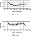
- FIG. 5C is a diagram of INL (Integral Non-Linearity) of a source follower without any DC tracking circuit.
- INL Integral Non-Linearity
- 5D is a diagram of INL of the source follower 100 with the DC tracking circuit 110 according to an embodiment of the invention.
- THD Total Harmonic Distortion
- 61.96dB without the DC tracking circuit 110
- 66.96dB with the DC tracking circuit 110
- INL improves from 0.76LSB (Least Significant Bit) (without the DC tracking circuit 110, as shown in FIG. 5C ) to 0.5LSB (with the DC tracking circuit 110, as shown in FIG. 5D ). Therefore, the proposed source follower 100 with the DC tracking circuit 110 can effectively suppress its second harmonic distortion and enhance its device linearity.
- FIG. 6 is a diagram of a source follower 600 according to another embodiment of the invention.
- the source follower 600 includes a first transistor M1' and a second transistor M2' which are PMOS transistors (P-type Metal-Oxide-Semiconductor Field-Effect Transistors).
- the input node NIN of the source follower 600 is coupled to the control terminal of the second transistor M2', such that the second transistor M2' is used as an input transistor.
- the bias voltage VB is coupled to the control terminal of the first transistor M1', such that the first transistor M1 is used as a current source.
- the second harmonic distortion relative to the source follower 600 can be almost eliminated.
- Other features of the source follower 600 of FIG. 6 are similar to those of the source follower 100 of FIG. 1 . Accordingly, the two embodiments can achieve similar levels of performance.
- FIG. 7 is a diagram of a source follower 700 according to an embodiment of the invention.
- the source follower 700 with an input node NIN and an output node NOUT includes a first transistor M1, a second transistor M2, and a DC (Direct Current) tracking circuit 710.
- the first transistor M1 and the second transistor M2 are NMOS transistors (N-type Metal-Oxide-Semiconductor Field-Effect Transistors).
- the first transistor M1 has a control terminal, a first terminal coupled to a first node N1, and a second terminal coupled to a supply voltage VDD.
- the input node NIN of the source follower 700 is coupled to the control terminal of the first transistor M1, and the output node NOUT of the source follower 700 is coupled to the first node N1, such that the first transistor M1 is used as an input transistor.
- the second transistor M2 has a control terminal, a first terminal coupled to a second node N2, and a second terminal coupled to the first node N1.
- a bias voltage VB is coupled to the control terminal of the second transistor M2, such that the second transistor M2 is used as a current source.
- the DC tracking circuit 710 sets a second DC voltage VD2 at the second node N2 to a specific level. The specific level is determined by the DC tracking circuit 710 according to a first DC voltage VD1 at the first node N1.
- the second DC voltage VD2 is substantially equal to two times the first DC voltage VD1 minus the supply voltage VDD, and their relationship is expressed as the equation (2).
- VD 2 2 ⁇ VD 1 ⁇ VDD wherein the symbol "VD1" represents the voltage level of the first DC voltage VD1, the symbol “VD2” represents the voltage level of the second DC voltage VD2, and the symbol “VDD” represents the voltage level of the supply voltage VDD.
- Other features of the source follower 700 of FIG. 7 are similar to those of the source follower 100 of FIG. 1 . Accordingly, the two embodiments can achieve similar levels of performance.
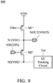
- FIG. 8 is a diagram of a source follower 800 according to another embodiment of the invention.
- the source follower 800 includes a first transistor M1' and a second transistor M2' which are PMOS transistors (P-type Metal-Oxide-Semiconductor Field-Effect Transistors).
- the input node NIN of the source follower 800 is coupled to the control terminal of the second transistor M2', such that the second transistor M2' is used as an input transistor.
- the bias voltage VB is coupled to the control terminal of the first transistor M1' such that the first transistor M1' is used as a current source.
- VDD - VD1 VDD - VD1
- the invention proposes a novel source follower for suppressing its relative second harmonic distortion.
- a DC tracking circuit is added and used to equalize the variation of drain-to-source voltage of an input transistor and a current source of the source follower.
- Such a design keeps the second harmonic distortion at a relatively low level.
- the proposed source follower of the invention is insensitive to the PVT (Process, Voltage, and Temperature) variations.
- the source follower of the invention is not limited to the configurations of FIGS. 1-8 .
- the invention may merely include any one or more features of any one or more embodiments of FIGS. 1-8 . In other words, not all of the features displayed in the figures should be implemented in the source follower.
Landscapes
- Engineering & Computer Science (AREA)
- Power Engineering (AREA)
- Physics & Mathematics (AREA)
- Computer Hardware Design (AREA)
- Computing Systems (AREA)
- General Engineering & Computer Science (AREA)
- Mathematical Physics (AREA)
- Nonlinear Science (AREA)
- Amplifiers (AREA)
Abstract
Description
- The disclosure generally relates to a source follower, and more specifically, to a source follower for suppressing second harmonic distortion.
- Conventionally, a single-input-ended source follower is very sensitive to PVT (Process, Voltage, and Temperature) variations, which are the result of second harmonic distortion relative to the source follower. The second harmonic distortion becomes worse when the variations of drain-to-source voltage of the input transistor and the current source are not symmetry to output-common mode voltage. Serious second harmonic distortion may degrade the linearity of the source follower, thereby negatively affecting its performance. Accordingly, there is a need to propose a novel solution to the problems with the prior art.
- In an embodiment, the disclosure is directed to a source follower with an input node and an output node, and the source follower includes a first transistor, a second transistor, and a DC (Direct Current) tracking circuit. The first transistor has a control terminal, a first terminal coupled to a first node, and a second terminal coupled to a second node. The second transistor has a control terminal, a first terminal coupled to a ground voltage, and a second terminal coupled to the first node. The DC tracking circuit sets a second DC voltage at the second node to a specific level. The specific level is determined according to a first DC voltage at the first node. The output node of the source follower is coupled to the first node.
- In some embodiments, the second DC voltage is substantially equal to two times the first DC voltage.
- In some embodiments, the DC tracking circuit is implemented with an open-loop operational amplifier, a closed-loop operational amplifier, or a linear regulator.
- In some embodiments, the input node of the source follower is coupled to the control terminal of the first transistor, and a bias voltage is coupled to the control terminal of the second transistor.
- In some embodiments, the first transistor and the second transistor are NMOS transistors (N-type Metal-Oxide-Semiconductor Field-Effect Transistors).
- In some embodiments, the DC tracking circuit includes a first operational amplifier, a third transistor, a fourth transistor, a first resistor, a second resistor, and a second operational amplifier. The first operational amplifier has a positive input terminal for receiving a first DC reference voltage, a negative input terminal coupled to a third node, and an output terminal coupled to a fourth node. The third transistor has a control terminal coupled to the fourth node, a first terminal coupled to a fifth node, and a second terminal coupled to a supply voltage. The fourth transistor has a control terminal coupled to the fourth node, a first terminal coupled to the second node, and a second terminal coupled to the supply voltage. The first resistor is coupled between the fifth node and the third node. The second resistor is coupled between the third node and the ground voltage. The second operational amplifier has a positive input terminal for receiving the first DC reference voltage, a negative input terminal for receiving a second DC reference voltage, and an output terminal coupled to the input node of the source follower.
- In some embodiments, both the first DC voltage and the second DC reference voltage are equal to the first DC reference voltage.
- In some embodiments, the third transistor and the fourth transistor are NMOS transistors (N-type Metal-Oxide-Semiconductor Field-Effect Transistors).
- In some embodiments, a DC component of an output voltage at the output node of the source follower is fed back to the second DC reference voltage.
- In some embodiments, the input node of the source follower is coupled to the control terminal of the second transistor, and a bias voltage is coupled to the control terminal of the first transistor.
- In some embodiments, the first transistor and the second transistor are PMOS transistors (P-type Metal-Oxide-Semiconductor Field-Effect Transistors).
- In another preferred embodiment, the invention is directed to a source follower with an input node and an output node, and the source follower includes a first transistor, a second transistor, and a DC (Direct Current) tracking circuit. The first transistor has a control terminal, a first terminal coupled to a first node, and a second terminal coupled to a supply voltage. The second transistor has a control terminal, a first terminal coupled to a second node, and a second terminal coupled to the first node. The DC tracking circuit sets the second DC voltage at the second node to a specific level. The specific level is determined according to the first DC voltage at the first node. The output node of the source follower is coupled to the first node.
- In some embodiments, the second DC voltage is substantially equal to two times the first DC voltage minus the supply voltage.
- The invention can be more fully understood by reading the subsequent detailed description and examples with references made to the accompanying drawings, wherein:
-
FIG. 1 is a diagram of a source follower according to an embodiment of the invention; -
FIG. 2A is a diagram of an open-loop operational amplifier according to an embodiment of the invention; -
FIG. 2B is a diagram of a closed-loop operational amplifier according to an embodiment of the invention; -
FIG. 2C is a diagram of a linear regulator according to an embodiment of the invention; -
FIG. 3 is a diagram of a source follower according to an embodiment of the invention; -
FIG. 4 is a diagram of the relationship between drain-to-source voltages of transistors and a first DC (Direct Current) voltage according to an embodiment of the invention; -
FIG. 5A is a diagram of power spectral mass of a source follower without any DC tracking circuit -
FIG. 5B is a diagram of power spectral mass of a source follower with a DC tracking circuit according to an embodiment of the invention; -
FIG. 5C is a diagram of INL (Integral Non-Linearity) of a source follower without any DC tracking circuit; -
FIG. 5D is a diagram of INL of a source follower with a DC tracking circuit according to an embodiment of the invention -
FIG. 6 is a diagram of a source follower according to another embodiment of the invention; -
FIG. 7 is a diagram of a source follower according to an embodiment of the invention; and -
FIG. 8 is a diagram of a source follower according to another embodiment of the invention. - In order to illustrate the purposes, features and advantages of the invention, the embodiments and figures of the invention will be described in detail as follows.
- Certain terms are used throughout the description and following claims to refer to particular components. As one skilled in the art will appreciate, manufacturers may refer to a component by different names. This document does not intend to distinguish between components that differ in name but not function. In the following description and in the claims, the terms "include" and "comprise" are used in an openended fashion, and thus should be interpreted to mean "include, but not limited to...". The term "substantially" means the value is within an acceptable error range. One skilled in the art can solve the technical problem within a predetermined error range and achieve the proposed technical performance. Also, the term "couple" is intended to mean either an indirect or direct electrical connection. Accordingly, if one device is coupled to another device, that connection may be through a direct electrical connection, or through an indirect electrical connection via other devices and connections.
-
FIG. 1 is a diagram of asource follower 100 according to an embodiment of the invention. As shown inFIG. 1 , thesource follower 100 with an input node NIN and an output node NOUT includes a first transistor M1, a second transistor M2, and a DC (Direct Current) trackingcircuit 110. The input node NIN of thesource follower 100 is arranged for receiving an input voltage VIN, and the output node NOUT of thesource follower 100 is arranged for outputting an output voltage VOUT. Generally, the waveform of the output voltage VOUT substantially follows the waveform of the input voltage VIN. - In the embodiment of
FIG. 1 , the first transistor M1 and the second transistor M2 are NMOS transistors (N-type Metal-Oxide-Semiconductor Field-Effect Transistors). The first transistor M1 and the second transistor M2 may have the same transistor sizes. The first transistor M1 has a control terminal, a first terminal coupled to a first node N1, and a second terminal coupled to a second node N2. The input node NIN of thesource follower 100 is coupled to the control terminal of the first transistor M1, and the output node NOUT of thesource follower 100 is coupled to the first node N1, such that the first transistor M1 is used as an input transistor. The second transistor M2 has a control terminal, a first terminal coupled to a ground voltage VSS, and a second terminal coupled to the first node N1. A bias voltage VB is coupled to the control terminal of the second transistor M2, such that the second transistor M2 is used as a current source. TheDC tracking circuit 110 sets a second DC voltage VD2 at the second node N2 to a specific level. For example, the specific level may be constant or dynamic. The specific level is determined by theDC tracking circuit 110 according to a first DC voltage VD1 at the first node N1. - In some embodiments, the second DC voltage VD2 is substantially equal to two times the first DC voltage VD1, and their relationship is expressed as the equation (1).

- The
DC tracking circuit 110 may have a plurality different configurations.FIG. 2A is a diagram of an open-loopoperational amplifier 210 according to an embodiment of the invention.FIG. 2B is a diagram of a closed-loopoperational amplifier 220 according to an embodiment of the invention.FIG. 2C is a diagram of alinear regulator 230 according to an embodiment of the invention. The aforementioned amplifiers and regulator can clamp the second DC voltage VD2 to a specific level. For example, theDC tracking circuit 110 may be implemented with the open-loopoperational amplifier 210, the closed-loopoperational amplifier 220, or thelinear regulator 230, as shown inFIG. 2A, FIG, 2B, and FIG, 2C , but it is not limited thereto. Accordingly, the second DC voltage VD2 is determined in response to the first DC voltage VD1. -
FIG. 3 is a diagram of asource follower 300 according to an embodiment of the invention. In the embodiment ofFIG. 3 , thesource follower 300 includes a first transistor M1, a second transistor M2, and aDC tracking circuit 310, which is implemented with a regulator including two operational amplifiers. The arrangements and functions of the first transistor M1 and the second transistor M2 have been described in the embodiment ofFIG. 1 . TheDC tracking circuit 310 can determine the second DC voltage VD2 according to the first DC voltage VD1, as mentioned above. Specifically, theDC tracking circuit 310 includes a firstoperational amplifier 320, a secondoperational amplifier 330, a third transistor M3, a fourth transistor M4, a first resistor R1, and a second resistor R2. The third transistor M3 and the fourth transistor M4 may be NMOS transistors (N-type Metal-Oxide-Semiconductor Field-Effect Transistors). The firstoperational amplifier 320 has a positive input terminal for receiving a first DC reference voltage VDR1, a negative input terminal coupled to a third node N3, and an output terminal coupled to a fourth node N4. The third transistor M3 has a control terminal coupled to the fourth node N4, a first terminal coupled to a fifth node N5, and a second terminal coupled to a supply voltage VDD. The fourth transistor M4 has a control terminal coupled to the fourth node N4, a first terminal coupled to the second node N2, and a second terminal coupled to the supply voltage VDD. The first resistor R1 and the second resistor R2 may have the same resistance. The first resistor R1 is coupled between the fifth node N5 and the third node N3. The second resistor R2 is coupled between the third node N3 and the ground voltage VSS. The secondoperational amplifier 330 has a positive input terminal for receiving the first DC reference voltage VDR1, a negative input terminal for receiving a second DC reference voltage VDR2, and an output terminal coupled to the input node NIN of thesource follower 300. Both the first DC voltage VD1 at the first node N1 and the second DC reference voltage VDR2 may be equal to the first DC reference voltage VDR1 due to close-loop. In some embodiments, theDC tracking circuit 310 further includes an AC (Alternating Current) filter 340 (optional element), and the output node NOUT of thesource follower 300 is fed back through theAC filter 340 to the second DC reference voltage VDR2. As a result, the second DC reference voltage VDR2 may include only a DC component of the output voltage VOUT, and an AC component of the output voltage VOUT is completely removed by theAC filter 340. -
FIG. 4 is a diagram of the relationship between the drain-to-source voltages of transistors and the first DC voltage VD1 according to an embodiment of the invention. As shown inFIG. 4 , thefirst curve 401 represents the drain-to-source voltage of the first transistor M1, and thesecond curve 402 represents the drain-to-source voltage of the second transistor M2. According to the measurement ofFIG. 4 , if the first DC voltage VD1 becomes higher, the drain-to-source voltage of the first transistor M1 will decrease, but the drain-to-source voltage of the second transistor M2 will increase; conversely, if the first DC voltage VD1 becomes lower, the drain-to-source voltage of the first transistor M1 will increase, but the drain-to-source voltage of the second transistor M2 will decrease. That is, the total drain-to-source voltage of the first transistor M1 and the second transistor M2 are substantially maintained at a relatively constant level. At theintersection point 450 of thefirst curve 401 and thesecond curve 402, the first transistor M1 and the second transistor M2 can have the same drain-to-source resistances. Please refer to the embodiment ofFIG. 1 again. By using theDC tracking circuit 110 to clamp the second DC voltage VD2, a first DC voltage difference (i.e., VD2 - VD1 = VD1) across the first transistor M1 can be substantially equal to a second DC voltage difference (i.e., VD1 - VSS = VD1) across the second transistor M2. Since the variations in the drain-to-source voltages of the first transistor M1 and the second transistor M2 are nearly symmetry to the output-common mode voltage (i.e., the first DC voltage VD1 at the first node), the second harmonic distortion relative to thesource follower 100 can almost be eliminated. -
FIG. 5A is a diagram of power spectral mass of a source follower without any DC tracking circuit.FIG. 5B is a diagram of power spectral mass of thesource follower 100 with theDC tracking circuit 110 according to an embodiment of the invention. The horizontal axis represents the operation frequency (MHz), and the vertical axis represents the power spectral mass (dB) relative to the source follower. According to the measurement ofFIG. 5A andFIG. 5B , when theDC tracking circuit 110 is applied to thesource follower 100, the strength of a second harmonic component 520 (with respect to a fundamental component 510) is significantly suppressed.FIG. 5C is a diagram of INL (Integral Non-Linearity) of a source follower without any DC tracking circuit.FIG. 5D is a diagram of INL of thesource follower 100 with theDC tracking circuit 110 according to an embodiment of the invention. Detailed measurement data show further that the THD (Total Harmonic Distortion) improves from 61.96dB (without the DC tracking circuit 110) to 66.96dB (with the DC tracking circuit 110), and the INL improves from 0.76LSB (Least Significant Bit) (without theDC tracking circuit 110, as shown inFIG. 5C ) to 0.5LSB (with theDC tracking circuit 110, as shown inFIG. 5D ). Therefore, the proposedsource follower 100 with theDC tracking circuit 110 can effectively suppress its second harmonic distortion and enhance its device linearity. -
FIG. 6 is a diagram of asource follower 600 according to another embodiment of the invention.FIG. 6 is similar toFIG. 1 . In the embodiments ofFIG. 6 , thesource follower 600 includes a first transistor M1' and a second transistor M2' which are PMOS transistors (P-type Metal-Oxide-Semiconductor Field-Effect Transistors). The input node NIN of thesource follower 600 is coupled to the control terminal of the second transistor M2', such that the second transistor M2' is used as an input transistor. The bias voltage VB is coupled to the control terminal of the first transistor M1', such that the first transistor M1 is used as a current source. Similarly, theDC tracking circuit 110 can clamp the second DC voltage VD2, and therefore the first DC voltage difference (i.e., VD2 - VD1 = VD1) across the first transistor M1' can be substantially equal to the second DC voltage difference (i.e., VD1 - VSS = VD1) across the second transistor M2'. As a result, the second harmonic distortion relative to thesource follower 600 can be almost eliminated. Other features of thesource follower 600 ofFIG. 6 are similar to those of thesource follower 100 ofFIG. 1 . Accordingly, the two embodiments can achieve similar levels of performance. -
FIG. 7 is a diagram of asource follower 700 according to an embodiment of the invention. As shown inFIG. 7 , thesource follower 700 with an input node NIN and an output node NOUT includes a first transistor M1, a second transistor M2, and a DC (Direct Current) trackingcircuit 710. In the embodiment ofFIG. 7 , the first transistor M1 and the second transistor M2 are NMOS transistors (N-type Metal-Oxide-Semiconductor Field-Effect Transistors). The first transistor M1 has a control terminal, a first terminal coupled to a first node N1, and a second terminal coupled to a supply voltage VDD. The input node NIN of thesource follower 700 is coupled to the control terminal of the first transistor M1, and the output node NOUT of thesource follower 700 is coupled to the first node N1, such that the first transistor M1 is used as an input transistor. The second transistor M2 has a control terminal, a first terminal coupled to a second node N2, and a second terminal coupled to the first node N1. A bias voltage VB is coupled to the control terminal of the second transistor M2, such that the second transistor M2 is used as a current source. TheDC tracking circuit 710 sets a second DC voltage VD2 at the second node N2 to a specific level. The specific level is determined by theDC tracking circuit 710 according to a first DC voltage VD1 at the first node N1. - In some embodiments, the second DC voltage VD2 is substantially equal to two times the first DC voltage VD1 minus the supply voltage VDD, and their relationship is expressed as the equation (2).

- For the
source follower 700, by using theDC tracking circuit 710 to clamp the second DC voltage VD2, a third DC voltage difference (i.e., VDD - VD1) across the first transistor M1 can be substantially equal to a fourth DC voltage difference (i.e., VD1 - VD2 = VDD - VD1) across the second transistor M2. Since the variation of drain-to-source voltage of first transistor M1 and the second transistor M2 are nearly symmetry to output-common mode voltage,, the second harmonic distortion relative to thesource follower 700 can almost be eliminated. Other features of thesource follower 700 ofFIG. 7 are similar to those of thesource follower 100 ofFIG. 1 . Accordingly, the two embodiments can achieve similar levels of performance. -
FIG. 8 is a diagram of asource follower 800 according to another embodiment of the invention.FIG. 8 is similar toFIG. 7 . In the embodiments ofFIG. 8 , thesource follower 800 includes a first transistor M1' and a second transistor M2' which are PMOS transistors (P-type Metal-Oxide-Semiconductor Field-Effect Transistors). The input node NIN of thesource follower 800 is coupled to the control terminal of the second transistor M2', such that the second transistor M2' is used as an input transistor. The bias voltage VB is coupled to the control terminal of the first transistor M1' such that the first transistor M1' is used as a current source. Similarly, theDC tracking circuit 110 can clamp the second DC voltage VD2, and therefore the third DC voltage difference (i.e., VDD - VD1) across the first transistor M1' can be substantially equal to the fourth DC voltage difference (i.e., VD1 - VD2 = VDD - VD1) across the second transistor M2'. As a result, the second harmonic distortion relative to thesource follower 800 can almost be eliminated. Other features of thesource follower 800 ofFIG. 8 are similar to those of thesource follower 700 ofFIG. 7 . Accordingly, the two embodiments can achieve similar levels of performance. - The invention proposes a novel source follower for suppressing its relative second harmonic distortion. A DC tracking circuit is added and used to equalize the variation of drain-to-source voltage of an input transistor and a current source of the source follower. Such a design keeps the second harmonic distortion at a relatively low level. Accordingly, the proposed source follower of the invention is insensitive to the PVT (Process, Voltage, and Temperature) variations.
- Note that the above voltages, currents, resistances, inductances, capacitances and other element parameters are not limitations of the invention. A designer can adjust these parameters according to different requirements. The source follower of the invention is not limited to the configurations of
FIGS. 1-8 . The invention may merely include any one or more features of any one or more embodiments ofFIGS. 1-8 . In other words, not all of the features displayed in the figures should be implemented in the source follower. - Use of ordinal terms such as "first", "second", "third", etc., in the claims to modify a claim element does not by itself connote any priority, precedence, or order of one claim element over another or the temporal order in which acts of a method are performed, but are used merely as labels to distinguish one claim element having a certain name from another element having the same name (but for use of the ordinal term) to distinguish the claim elements.
- While the invention has been described by way of example and in terms of the preferred embodiments, it is to be understood that the invention is not limited to the disclosed embodiments. On the contrary, it is intended to cover various modifications and similar arrangements (as would be apparent to those skilled in the art). Therefore, the scope of the appended claims should be accorded the broadest interpretation so as to encompass all such modifications and similar arrangements.
Claims (13)
- A source follower (100, 300, 600, 700, 800), comprising:a first transistor (M1), comprising a control terminal, a first terminal coupled to an output node (N1) of the source follower (100, 300, 600, 700, 800), and a second terminal coupled to a DC (Direct Current) tracking circuit (110, 310, 710); anda second transistor (M2), comprising a control terminal, a first terminal coupled to ground, and a second terminal coupled to the output node (N1);wherein the DC tracking circuit (110, 310, 710) is arranged for providing a second voltage, and wherein a level of the second voltage is determined according to a first voltage at the output node (N1).
- The source follower (100, 300, 600, 700, 800) as claimed in claim 1, wherein the second voltage is substantially equal to two times the first voltage.
- The source follower (100, 300, 600, 700, 800) as claimed in claim 1 or 2, wherein the DC tracking circuit (110, 310, 710) comprises an open-loop operational amplifier (210), a closed-loop operational amplifier (220), or a linear regulator (230).
- The source follower (100, 300, 600, 700, 800) as claimed in anyone of claims 1 to 3, wherein an input node (N2) of the source follower (100, 300, 600, 700, 800) is coupled to the control terminal of the first transistor (M1), and a bias voltage is coupled to the control terminal of the second transistor (M2).
- The source follower (100, 300, 600, 700, 800) as claimed in claim 4, wherein the first transistor (M1) and the second transistor (M2) are NMOS transistors (N-type Metal-Oxide-Semiconductor Field-Effect Transistors).
- The source follower (100, 300, 600, 700, 800) as claimed in claim 1, wherein the DC tracking circuit (110, 310, 710) comprises:a first operational amplifier (320), comprising a first input terminal for receiving a first reference voltage, a second input terminal, and an output terminal;a fourth transistor (M4), comprising a control terminal coupled to the output terminal of the first operational amplifier (320), and a second terminal coupled to a supply voltage; anda second operational amplifier (330), comprising a first input terminal for receiving the first reference voltage, a second input terminal for receiving a second reference voltage, and an output terminal coupled to an input node (N2) of the source follower (100, 300, 600, 700, 800).
- The source follower (100, 300, 600, 700, 800) as claimed in claim 6, wherein the DC tracking circuit (110, 310, 710) further comprises:a third transistor (M3), comprising a control terminal coupled to the output terminal of the first operational amplifier (320), a first terminal, and a second terminal coupled to the supply voltage;wherein the fourth transistor further comprises a first terminal coupled to the first transistor (M1).
- The source follower (100, 300, 600, 700, 800) as claimed in claim 7, wherein the DC tracking circuit (110, 310, 710) further comprises:a first resistor (R1), coupled between the fifth node (N5) and the third node (N3); anda second resistor (R2), coupled between the third node (N3) and the ground voltage.
- The source follower (100, 300, 600, 700, 800) as claimed in claim 7, wherein both the first voltage and the second reference voltage are equal to the first reference voltage.
- The source follower (100, 300, 600, 700, 800) as claimed in claim 7 or 8, wherein the third transistor (M3) and the fourth transistor (M4) are NMOS transistors (N-type Metal-Oxide-Semiconductor Field-Effect Transistors).
- The source follower (100, 300, 600, 700, 800) as claimed in any one of claims 7 to 10, wherein a DC component of an output voltage at the output node (N1) of the source follower is fed back to the second reference voltage.
- The source follower (100, 300, 600, 700, 800) as claimed in any one of the preceding claims, wherein an input node (N2) of the source follower (100, 300, 600, 700, 800) is coupled to the control terminal of the second transistor (M2), and a bias voltage is coupled to the control terminal of the first transistor (M1).
- The source follower (100, 300, 600, 700, 800) as claimed in claim 12, wherein the first transistor (M1) and the second transistor (M2) are PMOS transistors (P-type Metal-Oxide-Semiconductor Field-Effect Transistors).
Applications Claiming Priority (2)
| Application Number | Priority Date | Filing Date | Title |
|---|---|---|---|
| US201662431459P | 2016-12-08 | 2016-12-08 | |
| US15/810,942 US10476447B2 (en) | 2016-12-08 | 2017-11-13 | Source follower |
Publications (2)
| Publication Number | Publication Date |
|---|---|
| EP3334039A1 true EP3334039A1 (en) | 2018-06-13 |
| EP3334039B1 EP3334039B1 (en) | 2021-11-03 |
Family
ID=60627506
Family Applications (1)
| Application Number | Title | Priority Date | Filing Date |
|---|---|---|---|
| EP17205766.3A Active EP3334039B1 (en) | 2016-12-08 | 2017-12-06 | Source follower |
Country Status (4)
| Country | Link |
|---|---|
| US (2) | US10476447B2 (en) |
| EP (1) | EP3334039B1 (en) |
| CN (1) | CN108183704B (en) |
| TW (1) | TWI644509B (en) |
Families Citing this family (1)
| Publication number | Priority date | Publication date | Assignee | Title |
|---|---|---|---|---|
| TWI722900B (en) * | 2020-05-14 | 2021-03-21 | 絡達科技股份有限公司 | Power switch control circuit |
Citations (6)
| Publication number | Priority date | Publication date | Assignee | Title |
|---|---|---|---|---|
| US4646002A (en) * | 1984-05-10 | 1987-02-24 | Regents Of The University Of Minnesota | Circuit for high impedance broad band probe |
| EP0561336A1 (en) * | 1992-03-18 | 1993-09-22 | Eastman Kodak Company | High-sensitivity, low-noise transistor amplifier |
| US5254956A (en) * | 1991-05-29 | 1993-10-19 | Nec Corporation | Composite differential amplifier |
| EP0618673A2 (en) * | 1993-03-29 | 1994-10-05 | SANYO ELECTRIC Co., Ltd. | A differential amplification circuit wherein a DC level at an output terminal is automatically adjusted and a power amplifier wherein a BTL drive circuit is driven by a half wave |
| JP2002353743A (en) * | 2001-05-30 | 2002-12-06 | Matsushita Electric Ind Co Ltd | Audio output control circuit |
| US7088393B1 (en) * | 1998-09-21 | 2006-08-08 | Samsung Electronics Co., Ltd. | Output-compensated buffers with source-follower input structure, methods of operating same, and image capture devices using same |
Family Cites Families (9)
| Publication number | Priority date | Publication date | Assignee | Title |
|---|---|---|---|---|
| GB1546191A (en) * | 1975-08-25 | 1979-05-16 | Hewlett Packard Co | Peak detector |
| US4459553A (en) * | 1982-02-11 | 1984-07-10 | Tektronix, Inc. | D.C. Stabilization circuit for a follower-type amplifier |
| JPS63199507A (en) * | 1987-02-13 | 1988-08-18 | Nec Corp | Output stage circuit |
| US5055797A (en) * | 1989-04-03 | 1991-10-08 | Chater William T | Bias control for power amplifiers |
| US5874840A (en) | 1996-04-26 | 1999-02-23 | International Business Machines Corporation | Differential source follower with body effect compensation |
| US7221194B2 (en) * | 2005-02-18 | 2007-05-22 | Tpo Displays Corp. | Analog buffers composed of thin film transistors |
| US8390335B2 (en) | 2009-06-24 | 2013-03-05 | Futurewei Technologies, Inc. | Signal buffer amplifier |
| US9013226B2 (en) * | 2012-09-26 | 2015-04-21 | Texas Instruments Incorporated | Circuits for improving linearity of metal oxide semiconductor (MOS) transistors |
| JP6306343B2 (en) * | 2013-12-25 | 2018-04-04 | 株式会社半導体エネルギー研究所 | Source follower |
-
2017
- 2017-11-13 US US15/810,942 patent/US10476447B2/en active Active
- 2017-11-21 CN CN201711167282.4A patent/CN108183704B/en active Active
- 2017-11-22 TW TW106140529A patent/TWI644509B/en not_active IP Right Cessation
- 2017-12-06 EP EP17205766.3A patent/EP3334039B1/en active Active
-
2019
- 2019-09-30 US US16/589,085 patent/US10700647B2/en active Active
Patent Citations (6)
| Publication number | Priority date | Publication date | Assignee | Title |
|---|---|---|---|---|
| US4646002A (en) * | 1984-05-10 | 1987-02-24 | Regents Of The University Of Minnesota | Circuit for high impedance broad band probe |
| US5254956A (en) * | 1991-05-29 | 1993-10-19 | Nec Corporation | Composite differential amplifier |
| EP0561336A1 (en) * | 1992-03-18 | 1993-09-22 | Eastman Kodak Company | High-sensitivity, low-noise transistor amplifier |
| EP0618673A2 (en) * | 1993-03-29 | 1994-10-05 | SANYO ELECTRIC Co., Ltd. | A differential amplification circuit wherein a DC level at an output terminal is automatically adjusted and a power amplifier wherein a BTL drive circuit is driven by a half wave |
| US7088393B1 (en) * | 1998-09-21 | 2006-08-08 | Samsung Electronics Co., Ltd. | Output-compensated buffers with source-follower input structure, methods of operating same, and image capture devices using same |
| JP2002353743A (en) * | 2001-05-30 | 2002-12-06 | Matsushita Electric Ind Co Ltd | Audio output control circuit |
Non-Patent Citations (1)
| Title |
|---|
| CHAN P K ET AL: "Analysis and Design of Low-Distortion CMOS Source Followers", IEEE TRANSACTIONS ON CIRCUITS AND SYSTEMS PART I: REGULAR PAPERS, IEEE SERVICE CENTER, NEW YORK, NY, US, vol. 52, no. 8, 1 August 2005 (2005-08-01), pages 1489 - 1501, XP011137958, ISSN: 1057-7122, DOI: 10.1109/TCSI.2005.851711 * |
Also Published As
| Publication number | Publication date |
|---|---|
| US10700647B2 (en) | 2020-06-30 |
| US20180167036A1 (en) | 2018-06-14 |
| TWI644509B (en) | 2018-12-11 |
| TW201822459A (en) | 2018-06-16 |
| US10476447B2 (en) | 2019-11-12 |
| US20200036347A1 (en) | 2020-01-30 |
| CN108183704B (en) | 2022-04-26 |
| EP3334039B1 (en) | 2021-11-03 |
| CN108183704A (en) | 2018-06-19 |
Similar Documents
| Publication | Publication Date | Title |
|---|---|---|
| US7755339B2 (en) | Regulator with error amplifier having low voltage and high voltage transistors | |
| US20120044021A1 (en) | Differential amplifier circuit | |
| JP6211887B2 (en) | Voltage regulator | |
| US10551864B2 (en) | Bandgap voltage reference circuit | |
| US10474173B2 (en) | Voltage regulator having a phase compensation circuit | |
| US10558232B2 (en) | Regulator circuit and control method | |
| US9246479B2 (en) | Low-offset bandgap circuit and offset-cancelling circuit therein | |
| US20140028274A1 (en) | Regulator | |
| US20130300393A1 (en) | Circuit of outputting temperature compensation power voltage from variable power and method thereof | |
| US10284144B2 (en) | Amplifier circuit of high response speed and related clamping method | |
| US20070252647A1 (en) | Operational amplifier | |
| US20150097543A1 (en) | Voltage regulator | |
| US9369098B2 (en) | Inverting amplifier | |
| EP3282581B1 (en) | Buffer stage and control circuit | |
| US9106189B2 (en) | Operational amplifier circuit and method for enhancing driving capacity thereof | |
| US10700647B2 (en) | Source follower | |
| US20080297254A1 (en) | Class ab amplifier | |
| US20130181777A1 (en) | Voltage regulator | |
| US7629846B2 (en) | Source follower circuit and semiconductor apparatus | |
| US8471636B2 (en) | Differential pair with constant offset | |
| US11171612B2 (en) | Gain modulation circuit | |
| US9654074B2 (en) | Variable gain amplifier circuit, controller of main amplifier and associated control method | |
| US10211839B2 (en) | System and method of automatic power control system and bias current control circuit | |
| JP2007257104A (en) | Series regulator | |
| US20170272061A1 (en) | Voltage clamping circuit |
Legal Events
| Date | Code | Title | Description |
|---|---|---|---|
| PUAI | Public reference made under article 153(3) epc to a published international application that has entered the european phase |
Free format text: ORIGINAL CODE: 0009012 |
|
| STAA | Information on the status of an ep patent application or granted ep patent |
Free format text: STATUS: THE APPLICATION HAS BEEN PUBLISHED |
|
| AK | Designated contracting states |
Kind code of ref document: A1 Designated state(s): AL AT BE BG CH CY CZ DE DK EE ES FI FR GB GR HR HU IE IS IT LI LT LU LV MC MK MT NL NO PL PT RO RS SE SI SK SM TR |
|
| AX | Request for extension of the european patent |
Extension state: BA ME |
|
| STAA | Information on the status of an ep patent application or granted ep patent |
Free format text: STATUS: REQUEST FOR EXAMINATION WAS MADE |
|
| 17P | Request for examination filed |
Effective date: 20181213 |
|
| RBV | Designated contracting states (corrected) |
Designated state(s): AL AT BE BG CH CY CZ DE DK EE ES FI FR GB GR HR HU IE IS IT LI LT LU LV MC MK MT NL NO PL PT RO RS SE SI SK SM TR |
|
| STAA | Information on the status of an ep patent application or granted ep patent |
Free format text: STATUS: EXAMINATION IS IN PROGRESS |
|
| 17Q | First examination report despatched |
Effective date: 20190423 |
|
| GRAJ | Information related to disapproval of communication of intention to grant by the applicant or resumption of examination proceedings by the epo deleted |
Free format text: ORIGINAL CODE: EPIDOSDIGR1 |
|
| GRAP | Despatch of communication of intention to grant a patent |
Free format text: ORIGINAL CODE: EPIDOSNIGR1 |
|
| INTG | Intention to grant announced |
Effective date: 20210423 |
|
| GRAP | Despatch of communication of intention to grant a patent |
Free format text: ORIGINAL CODE: EPIDOSNIGR1 |
|
| STAA | Information on the status of an ep patent application or granted ep patent |
Free format text: STATUS: GRANT OF PATENT IS INTENDED |
|
| INTC | Intention to grant announced (deleted) | ||
| INTG | Intention to grant announced |
Effective date: 20210525 |
|
| RAP3 | Party data changed (applicant data changed or rights of an application transferred) |
Owner name: MEDIATEK INC. |
|
| GRAS | Grant fee paid |
Free format text: ORIGINAL CODE: EPIDOSNIGR3 |
|
| GRAA | (expected) grant |
Free format text: ORIGINAL CODE: 0009210 |
|
| STAA | Information on the status of an ep patent application or granted ep patent |
Free format text: STATUS: THE PATENT HAS BEEN GRANTED |
|
| AK | Designated contracting states |
Kind code of ref document: B1 Designated state(s): AL AT BE BG CH CY CZ DE DK EE ES FI FR GB GR HR HU IE IS IT LI LT LU LV MC MK MT NL NO PL PT RO RS SE SI SK SM TR |
|
| REG | Reference to a national code |
Ref country code: GB Ref legal event code: FG4D |
|
| REG | Reference to a national code |
Ref country code: AT Ref legal event code: REF Ref document number: 1444900 Country of ref document: AT Kind code of ref document: T Effective date: 20211115 Ref country code: CH Ref legal event code: EP |
|
| REG | Reference to a national code |
Ref country code: IE Ref legal event code: FG4D |
|
| REG | Reference to a national code |
Ref country code: DE Ref legal event code: R096 Ref document number: 602017048638 Country of ref document: DE |
|
| REG | Reference to a national code |
Ref country code: LT Ref legal event code: MG9D |
|
| REG | Reference to a national code |
Ref country code: NL Ref legal event code: MP Effective date: 20211103 |
|
| REG | Reference to a national code |
Ref country code: AT Ref legal event code: MK05 Ref document number: 1444900 Country of ref document: AT Kind code of ref document: T Effective date: 20211103 |
|
| PG25 | Lapsed in a contracting state [announced via postgrant information from national office to epo] |
Ref country code: RS Free format text: LAPSE BECAUSE OF FAILURE TO SUBMIT A TRANSLATION OF THE DESCRIPTION OR TO PAY THE FEE WITHIN THE PRESCRIBED TIME-LIMIT Effective date: 20211103 Ref country code: LT Free format text: LAPSE BECAUSE OF FAILURE TO SUBMIT A TRANSLATION OF THE DESCRIPTION OR TO PAY THE FEE WITHIN THE PRESCRIBED TIME-LIMIT Effective date: 20211103 Ref country code: FI Free format text: LAPSE BECAUSE OF FAILURE TO SUBMIT A TRANSLATION OF THE DESCRIPTION OR TO PAY THE FEE WITHIN THE PRESCRIBED TIME-LIMIT Effective date: 20211103 Ref country code: BG Free format text: LAPSE BECAUSE OF FAILURE TO SUBMIT A TRANSLATION OF THE DESCRIPTION OR TO PAY THE FEE WITHIN THE PRESCRIBED TIME-LIMIT Effective date: 20220203 Ref country code: AT Free format text: LAPSE BECAUSE OF FAILURE TO SUBMIT A TRANSLATION OF THE DESCRIPTION OR TO PAY THE FEE WITHIN THE PRESCRIBED TIME-LIMIT Effective date: 20211103 |
|
| PG25 | Lapsed in a contracting state [announced via postgrant information from national office to epo] |
Ref country code: IS Free format text: LAPSE BECAUSE OF FAILURE TO SUBMIT A TRANSLATION OF THE DESCRIPTION OR TO PAY THE FEE WITHIN THE PRESCRIBED TIME-LIMIT Effective date: 20220303 Ref country code: SE Free format text: LAPSE BECAUSE OF FAILURE TO SUBMIT A TRANSLATION OF THE DESCRIPTION OR TO PAY THE FEE WITHIN THE PRESCRIBED TIME-LIMIT Effective date: 20211103 Ref country code: PT Free format text: LAPSE BECAUSE OF FAILURE TO SUBMIT A TRANSLATION OF THE DESCRIPTION OR TO PAY THE FEE WITHIN THE PRESCRIBED TIME-LIMIT Effective date: 20220303 Ref country code: PL Free format text: LAPSE BECAUSE OF FAILURE TO SUBMIT A TRANSLATION OF THE DESCRIPTION OR TO PAY THE FEE WITHIN THE PRESCRIBED TIME-LIMIT Effective date: 20211103 Ref country code: NO Free format text: LAPSE BECAUSE OF FAILURE TO SUBMIT A TRANSLATION OF THE DESCRIPTION OR TO PAY THE FEE WITHIN THE PRESCRIBED TIME-LIMIT Effective date: 20220203 Ref country code: NL Free format text: LAPSE BECAUSE OF FAILURE TO SUBMIT A TRANSLATION OF THE DESCRIPTION OR TO PAY THE FEE WITHIN THE PRESCRIBED TIME-LIMIT Effective date: 20211103 Ref country code: LV Free format text: LAPSE BECAUSE OF FAILURE TO SUBMIT A TRANSLATION OF THE DESCRIPTION OR TO PAY THE FEE WITHIN THE PRESCRIBED TIME-LIMIT Effective date: 20211103 Ref country code: HR Free format text: LAPSE BECAUSE OF FAILURE TO SUBMIT A TRANSLATION OF THE DESCRIPTION OR TO PAY THE FEE WITHIN THE PRESCRIBED TIME-LIMIT Effective date: 20211103 Ref country code: GR Free format text: LAPSE BECAUSE OF FAILURE TO SUBMIT A TRANSLATION OF THE DESCRIPTION OR TO PAY THE FEE WITHIN THE PRESCRIBED TIME-LIMIT Effective date: 20220204 Ref country code: ES Free format text: LAPSE BECAUSE OF FAILURE TO SUBMIT A TRANSLATION OF THE DESCRIPTION OR TO PAY THE FEE WITHIN THE PRESCRIBED TIME-LIMIT Effective date: 20211103 |
|
| PG25 | Lapsed in a contracting state [announced via postgrant information from national office to epo] |
Ref country code: SM Free format text: LAPSE BECAUSE OF FAILURE TO SUBMIT A TRANSLATION OF THE DESCRIPTION OR TO PAY THE FEE WITHIN THE PRESCRIBED TIME-LIMIT Effective date: 20211103 Ref country code: SK Free format text: LAPSE BECAUSE OF FAILURE TO SUBMIT A TRANSLATION OF THE DESCRIPTION OR TO PAY THE FEE WITHIN THE PRESCRIBED TIME-LIMIT Effective date: 20211103 Ref country code: RO Free format text: LAPSE BECAUSE OF FAILURE TO SUBMIT A TRANSLATION OF THE DESCRIPTION OR TO PAY THE FEE WITHIN THE PRESCRIBED TIME-LIMIT Effective date: 20211103 Ref country code: EE Free format text: LAPSE BECAUSE OF FAILURE TO SUBMIT A TRANSLATION OF THE DESCRIPTION OR TO PAY THE FEE WITHIN THE PRESCRIBED TIME-LIMIT Effective date: 20211103 Ref country code: DK Free format text: LAPSE BECAUSE OF FAILURE TO SUBMIT A TRANSLATION OF THE DESCRIPTION OR TO PAY THE FEE WITHIN THE PRESCRIBED TIME-LIMIT Effective date: 20211103 Ref country code: CZ Free format text: LAPSE BECAUSE OF FAILURE TO SUBMIT A TRANSLATION OF THE DESCRIPTION OR TO PAY THE FEE WITHIN THE PRESCRIBED TIME-LIMIT Effective date: 20211103 |
|
| REG | Reference to a national code |
Ref country code: CH Ref legal event code: PL |
|
| REG | Reference to a national code |
Ref country code: DE Ref legal event code: R097 Ref document number: 602017048638 Country of ref document: DE |
|
| PG25 | Lapsed in a contracting state [announced via postgrant information from national office to epo] |
Ref country code: MC Free format text: LAPSE BECAUSE OF FAILURE TO SUBMIT A TRANSLATION OF THE DESCRIPTION OR TO PAY THE FEE WITHIN THE PRESCRIBED TIME-LIMIT Effective date: 20211103 |
|
| PLBE | No opposition filed within time limit |
Free format text: ORIGINAL CODE: 0009261 |
|
| STAA | Information on the status of an ep patent application or granted ep patent |
Free format text: STATUS: NO OPPOSITION FILED WITHIN TIME LIMIT |
|
| REG | Reference to a national code |
Ref country code: BE Ref legal event code: MM Effective date: 20211231 |
|
| 26N | No opposition filed |
Effective date: 20220804 |
|
| PG25 | Lapsed in a contracting state [announced via postgrant information from national office to epo] |
Ref country code: LU Free format text: LAPSE BECAUSE OF NON-PAYMENT OF DUE FEES Effective date: 20211206 Ref country code: IE Free format text: LAPSE BECAUSE OF NON-PAYMENT OF DUE FEES Effective date: 20211206 Ref country code: AL Free format text: LAPSE BECAUSE OF FAILURE TO SUBMIT A TRANSLATION OF THE DESCRIPTION OR TO PAY THE FEE WITHIN THE PRESCRIBED TIME-LIMIT Effective date: 20211103 |
|
| PG25 | Lapsed in a contracting state [announced via postgrant information from national office to epo] |
Ref country code: SI Free format text: LAPSE BECAUSE OF FAILURE TO SUBMIT A TRANSLATION OF THE DESCRIPTION OR TO PAY THE FEE WITHIN THE PRESCRIBED TIME-LIMIT Effective date: 20211103 Ref country code: BE Free format text: LAPSE BECAUSE OF NON-PAYMENT OF DUE FEES Effective date: 20211231 |
|
| PG25 | Lapsed in a contracting state [announced via postgrant information from national office to epo] |
Ref country code: LI Free format text: LAPSE BECAUSE OF NON-PAYMENT OF DUE FEES Effective date: 20211231 Ref country code: CH Free format text: LAPSE BECAUSE OF NON-PAYMENT OF DUE FEES Effective date: 20211231 |
|
| PG25 | Lapsed in a contracting state [announced via postgrant information from national office to epo] |
Ref country code: IT Free format text: LAPSE BECAUSE OF FAILURE TO SUBMIT A TRANSLATION OF THE DESCRIPTION OR TO PAY THE FEE WITHIN THE PRESCRIBED TIME-LIMIT Effective date: 20211103 Ref country code: HU Free format text: LAPSE BECAUSE OF FAILURE TO SUBMIT A TRANSLATION OF THE DESCRIPTION OR TO PAY THE FEE WITHIN THE PRESCRIBED TIME-LIMIT; INVALID AB INITIO Effective date: 20171206 |
|
| PG25 | Lapsed in a contracting state [announced via postgrant information from national office to epo] |
Ref country code: CY Free format text: LAPSE BECAUSE OF FAILURE TO SUBMIT A TRANSLATION OF THE DESCRIPTION OR TO PAY THE FEE WITHIN THE PRESCRIBED TIME-LIMIT Effective date: 20211103 |
|
| P01 | Opt-out of the competence of the unified patent court (upc) registered |
Effective date: 20230607 |
|
| PG25 | Lapsed in a contracting state [announced via postgrant information from national office to epo] |
Ref country code: MK Free format text: LAPSE BECAUSE OF FAILURE TO SUBMIT A TRANSLATION OF THE DESCRIPTION OR TO PAY THE FEE WITHIN THE PRESCRIBED TIME-LIMIT Effective date: 20211103 |
|
| PG25 | Lapsed in a contracting state [announced via postgrant information from national office to epo] |
Ref country code: TR Free format text: LAPSE BECAUSE OF FAILURE TO SUBMIT A TRANSLATION OF THE DESCRIPTION OR TO PAY THE FEE WITHIN THE PRESCRIBED TIME-LIMIT Effective date: 20211103 |
|
| PG25 | Lapsed in a contracting state [announced via postgrant information from national office to epo] |
Ref country code: MT Free format text: LAPSE BECAUSE OF FAILURE TO SUBMIT A TRANSLATION OF THE DESCRIPTION OR TO PAY THE FEE WITHIN THE PRESCRIBED TIME-LIMIT Effective date: 20211103 |
|
| PGFP | Annual fee paid to national office [announced via postgrant information from national office to epo] |
Ref country code: FR Payment date: 20250930 Year of fee payment: 9 |
|
| PGFP | Annual fee paid to national office [announced via postgrant information from national office to epo] |
Ref country code: DE Payment date: 20250930 Year of fee payment: 9 |
|
| PGFP | Annual fee paid to national office [announced via postgrant information from national office to epo] |
Ref country code: GB Payment date: 20251001 Year of fee payment: 9 |