EP3333924A1 - Organic light emitting diode display and method of manufacturing the same - Google Patents
Organic light emitting diode display and method of manufacturing the same Download PDFInfo
- Publication number
- EP3333924A1 EP3333924A1 EP17205586.5A EP17205586A EP3333924A1 EP 3333924 A1 EP3333924 A1 EP 3333924A1 EP 17205586 A EP17205586 A EP 17205586A EP 3333924 A1 EP3333924 A1 EP 3333924A1
- Authority
- EP
- European Patent Office
- Prior art keywords
- electrode
- layer
- light emitting
- auxiliary
- emitting diode
- Prior art date
- Legal status (The legal status is an assumption and is not a legal conclusion. Google has not performed a legal analysis and makes no representation as to the accuracy of the status listed.)
- Granted
Links
Images






Classifications
-
- H—ELECTRICITY
- H10—SEMICONDUCTOR DEVICES; ELECTRIC SOLID-STATE DEVICES NOT OTHERWISE PROVIDED FOR
- H10K—ORGANIC ELECTRIC SOLID-STATE DEVICES
- H10K59/00—Integrated devices, or assemblies of multiple devices, comprising at least one organic light-emitting element covered by group H10K50/00
- H10K59/80—Constructional details
- H10K59/805—Electrodes
- H10K59/8052—Cathodes
- H10K59/80522—Cathodes combined with auxiliary electrodes
-
- H—ELECTRICITY
- H10—SEMICONDUCTOR DEVICES; ELECTRIC SOLID-STATE DEVICES NOT OTHERWISE PROVIDED FOR
- H10D—INORGANIC ELECTRIC SEMICONDUCTOR DEVICES
- H10D86/00—Integrated devices formed in or on insulating or conducting substrates, e.g. formed in silicon-on-insulator [SOI] substrates or on stainless steel or glass substrates
- H10D86/01—Manufacture or treatment
- H10D86/021—Manufacture or treatment of multiple TFTs
- H10D86/0221—Manufacture or treatment of multiple TFTs comprising manufacture, treatment or patterning of TFT semiconductor bodies
-
- H—ELECTRICITY
- H10—SEMICONDUCTOR DEVICES; ELECTRIC SOLID-STATE DEVICES NOT OTHERWISE PROVIDED FOR
- H10K—ORGANIC ELECTRIC SOLID-STATE DEVICES
- H10K50/00—Organic light-emitting devices
- H10K50/10—OLEDs or polymer light-emitting diodes [PLED]
- H10K50/11—OLEDs or polymer light-emitting diodes [PLED] characterised by the electroluminescent [EL] layers
-
- H—ELECTRICITY
- H10—SEMICONDUCTOR DEVICES; ELECTRIC SOLID-STATE DEVICES NOT OTHERWISE PROVIDED FOR
- H10K—ORGANIC ELECTRIC SOLID-STATE DEVICES
- H10K50/00—Organic light-emitting devices
- H10K50/80—Constructional details
- H10K50/805—Electrodes
- H10K50/82—Cathodes
- H10K50/824—Cathodes combined with auxiliary electrodes
-
- H—ELECTRICITY
- H10—SEMICONDUCTOR DEVICES; ELECTRIC SOLID-STATE DEVICES NOT OTHERWISE PROVIDED FOR
- H10K—ORGANIC ELECTRIC SOLID-STATE DEVICES
- H10K59/00—Integrated devices, or assemblies of multiple devices, comprising at least one organic light-emitting element covered by group H10K50/00
- H10K59/10—OLED displays
- H10K59/12—Active-matrix OLED [AMOLED] displays
- H10K59/1201—Manufacture or treatment
-
- H—ELECTRICITY
- H10—SEMICONDUCTOR DEVICES; ELECTRIC SOLID-STATE DEVICES NOT OTHERWISE PROVIDED FOR
- H10K—ORGANIC ELECTRIC SOLID-STATE DEVICES
- H10K59/00—Integrated devices, or assemblies of multiple devices, comprising at least one organic light-emitting element covered by group H10K50/00
- H10K59/10—OLED displays
- H10K59/12—Active-matrix OLED [AMOLED] displays
- H10K59/121—Active-matrix OLED [AMOLED] displays characterised by the geometry or disposition of pixel elements
- H10K59/1213—Active-matrix OLED [AMOLED] displays characterised by the geometry or disposition of pixel elements the pixel elements being TFTs
-
- H—ELECTRICITY
- H10—SEMICONDUCTOR DEVICES; ELECTRIC SOLID-STATE DEVICES NOT OTHERWISE PROVIDED FOR
- H10K—ORGANIC ELECTRIC SOLID-STATE DEVICES
- H10K59/00—Integrated devices, or assemblies of multiple devices, comprising at least one organic light-emitting element covered by group H10K50/00
- H10K59/10—OLED displays
- H10K59/12—Active-matrix OLED [AMOLED] displays
- H10K59/122—Pixel-defining structures or layers, e.g. banks
-
- H—ELECTRICITY
- H10—SEMICONDUCTOR DEVICES; ELECTRIC SOLID-STATE DEVICES NOT OTHERWISE PROVIDED FOR
- H10K—ORGANIC ELECTRIC SOLID-STATE DEVICES
- H10K59/00—Integrated devices, or assemblies of multiple devices, comprising at least one organic light-emitting element covered by group H10K50/00
- H10K59/10—OLED displays
- H10K59/12—Active-matrix OLED [AMOLED] displays
- H10K59/124—Insulating layers formed between TFT elements and OLED elements
-
- H—ELECTRICITY
- H10—SEMICONDUCTOR DEVICES; ELECTRIC SOLID-STATE DEVICES NOT OTHERWISE PROVIDED FOR
- H10K—ORGANIC ELECTRIC SOLID-STATE DEVICES
- H10K59/00—Integrated devices, or assemblies of multiple devices, comprising at least one organic light-emitting element covered by group H10K50/00
- H10K59/10—OLED displays
- H10K59/12—Active-matrix OLED [AMOLED] displays
- H10K59/131—Interconnections, e.g. wiring lines or terminals
-
- H—ELECTRICITY
- H10—SEMICONDUCTOR DEVICES; ELECTRIC SOLID-STATE DEVICES NOT OTHERWISE PROVIDED FOR
- H10K—ORGANIC ELECTRIC SOLID-STATE DEVICES
- H10K59/00—Integrated devices, or assemblies of multiple devices, comprising at least one organic light-emitting element covered by group H10K50/00
- H10K59/10—OLED displays
- H10K59/12—Active-matrix OLED [AMOLED] displays
- H10K59/131—Interconnections, e.g. wiring lines or terminals
- H10K59/1315—Interconnections, e.g. wiring lines or terminals comprising structures specially adapted for lowering the resistance
-
- H—ELECTRICITY
- H10—SEMICONDUCTOR DEVICES; ELECTRIC SOLID-STATE DEVICES NOT OTHERWISE PROVIDED FOR
- H10K—ORGANIC ELECTRIC SOLID-STATE DEVICES
- H10K59/00—Integrated devices, or assemblies of multiple devices, comprising at least one organic light-emitting element covered by group H10K50/00
- H10K59/30—Devices specially adapted for multicolour light emission
-
- H—ELECTRICITY
- H10—SEMICONDUCTOR DEVICES; ELECTRIC SOLID-STATE DEVICES NOT OTHERWISE PROVIDED FOR
- H10K—ORGANIC ELECTRIC SOLID-STATE DEVICES
- H10K59/00—Integrated devices, or assemblies of multiple devices, comprising at least one organic light-emitting element covered by group H10K50/00
- H10K59/30—Devices specially adapted for multicolour light emission
- H10K59/35—Devices specially adapted for multicolour light emission comprising red-green-blue [RGB] subpixels
-
- H—ELECTRICITY
- H10—SEMICONDUCTOR DEVICES; ELECTRIC SOLID-STATE DEVICES NOT OTHERWISE PROVIDED FOR
- H10K—ORGANIC ELECTRIC SOLID-STATE DEVICES
- H10K71/00—Manufacture or treatment specially adapted for the organic devices covered by this subclass
- H10K71/10—Deposition of organic active material
-
- H—ELECTRICITY
- H10—SEMICONDUCTOR DEVICES; ELECTRIC SOLID-STATE DEVICES NOT OTHERWISE PROVIDED FOR
- H10K—ORGANIC ELECTRIC SOLID-STATE DEVICES
- H10K71/00—Manufacture or treatment specially adapted for the organic devices covered by this subclass
- H10K71/20—Changing the shape of the active layer in the devices, e.g. patterning
- H10K71/211—Changing the shape of the active layer in the devices, e.g. patterning by selective transformation of an existing layer
-
- H—ELECTRICITY
- H10—SEMICONDUCTOR DEVICES; ELECTRIC SOLID-STATE DEVICES NOT OTHERWISE PROVIDED FOR
- H10K—ORGANIC ELECTRIC SOLID-STATE DEVICES
- H10K71/00—Manufacture or treatment specially adapted for the organic devices covered by this subclass
- H10K71/621—Providing a shape to conductive layers, e.g. patterning or selective deposition
-
- H—ELECTRICITY
- H10—SEMICONDUCTOR DEVICES; ELECTRIC SOLID-STATE DEVICES NOT OTHERWISE PROVIDED FOR
- H10K—ORGANIC ELECTRIC SOLID-STATE DEVICES
- H10K2102/00—Constructional details relating to the organic devices covered by this subclass
- H10K2102/10—Transparent electrodes, e.g. using graphene
- H10K2102/101—Transparent electrodes, e.g. using graphene comprising transparent conductive oxides [TCO]
- H10K2102/103—Transparent electrodes, e.g. using graphene comprising transparent conductive oxides [TCO] comprising indium oxides, e.g. ITO
-
- H—ELECTRICITY
- H10—SEMICONDUCTOR DEVICES; ELECTRIC SOLID-STATE DEVICES NOT OTHERWISE PROVIDED FOR
- H10K—ORGANIC ELECTRIC SOLID-STATE DEVICES
- H10K59/00—Integrated devices, or assemblies of multiple devices, comprising at least one organic light-emitting element covered by group H10K50/00
- H10K59/10—OLED displays
Definitions
- the present disclosure relates to a display device, and more particularly, to an organic light emitting diode (OLED) display device and a method of manufacturing the OLED display device.
- OLED organic light emitting diode
- LCDs liquid crystal displays
- PDPs plasma display panels
- OLED organic light emitting diode
- FEDs field effect displays
- EPDs electrophoretic displays
- the organic light emitting diode (OLED) display includes two electrodes and an organic emission layer disposed therebetween. Electrons from one electrode and holes from the other electrode combine within the organic emission layer to thereby form excitons, which release energy in the form of light as they relax.
- the organic light emitting diode (OLED) display accordingly has a self-luminous characteristic, and because the organic light emitting diode (OLED) display does not need a separate light source, unlike a liquid crystal display (LCD), the OLED display can be relatively thin and light weight. Further, the organic light emitting diode (OLED) display exhibits high-quality characteristics such as low power consumption, high luminance, and fast response speed, and thus receives attention as a next generation display device.
- the common electrode and a common voltage line are connected to each other in each sub-pixel.
- the common electrode and the common voltage line are electrically connected to each other by removing a part of an organic emission layer with a laser.
- a metal layer disposed under the organic emission layer may be damaged, and a remaining gas component of the organic layer may be discharged into the damaged metal layer such that the common electrode may be oxidized.
- the present invention provides an organic light emitting diode display and a manufacturing method for preventing the metal layer positioned under the organic emission layer from being damaged by the laser.
- the present invention provides an organic light emitting diode display and a manufacturing method for preventing the common electrode from being oxidized due to the discharge of the remaining gas of the organic layer due to the damaged metal layer.
- An organic light emitting diode display includes: a substrate; a pixel formed on the substrate and including a pixel area displaying an image and a peripheral area adjacent to the pixel area; an insulating layer formed at the pixel area and the peripheral area on the substrate; a first electrode formed at the pixel area on the insulating layer; an organic emission layer formed on the first electrode and extending to the peripheral area; a second electrode formed on the organic emission layer and disposed in the pixel area and the peripheral area; an auxiliary electrode disposed in the peripheral area on the substrate and partially exposed by a first opening formed in the insulating layer; and an auxiliary member disposed on the auxiliary electrode and in contact with an upper surface of the auxiliary electrode exposed by the first opening.
- the insulating layer may be a planarization layer which serves to planarize a step on a thin film transistor and to thereby increase emission efficiency of the organic light emitting element that will be formed thereon.
- the present invention is not restricted to such an embodiment and the insulating layer may be another layer than a planarization layer.
- the organic emission layer may be disposed on the auxiliary member in the peripheral area, and may have a second opening exposing part of the auxiliary member.
- the second electrode may be in contact with the auxiliary member through the second opening.
- the second opening may have a circular shape.
- the auxiliary member may cover the first opening of the insulating layer. This means that the auxiliary member may close the first opening in the insulating layer, whereby the auxiliary member may be plane or may additionally extend in a thickness direction of the insulating layer.
- the auxiliary member may be in contact with a part of an interior circumference of the first opening. Especially in this case the auxiliary member extends in a thickness direction of the insulating layer and at the same time may cover the first opening.
- the auxiliary member may be formed with the same layer as the first electrode.
- the auxiliary member may be formed by sequentially stacking ITO (indium tin oxide), silver (Ag), and ITO.
- the auxiliary electrode may be a common voltage line transmitting a common voltage.
- the auxiliary electrode may be formed by sequentially stacking molybdenum (Mo), aluminum (Al), and molybdenum (Mo).
- the pixel may include at least one sub-pixel including the pixel area and the peripheral area, and the sub-pixel may be a red sub-pixel.
- a manufacturing method of an organic light emitting diode display includes: preparing a substrate; forming a thin film transistor including a semiconductor layer, a gate electrode on the semiconductor layer, and a source electrode and a drain electrode connected to the semiconductor layer on the substrate; forming an auxiliary electrode supplying a common voltage on the substrate; forming an insulating layer on the thin film transistor and the auxiliary electrode and exposing parts of the drain electrode and the auxiliary electrode; forming a first electrode on the insulating layer and in contact with the drain electrode; forming an auxiliary member in contact with the auxiliary electrode through a first opening formed in the insulating layer; forming an organic emission layer on the first electrode and the auxiliary member; removing a part of the organic emission layer to expose a part of the auxiliary member; and forming a second electrode on the organic emission layer.
- the removal of the part of the organic emission layer may be performed by using a laser.
- the removal of the part of the organic emission layer may include forming a second opening by removing the part of the organic emission layer.
- the second opening may have a circular shape.
- the method may further include forming a pixel definition layer having a third opening exposing the part of the auxiliary member and a fourth opening exposing the part of the first electrode.
- the source electrode, the drain electrode, and the auxiliary electrode may be formed with the same layer.
- the first electrode and the auxiliary member may be formed with the same layer.
- the auxiliary member may be in contact with an entire upper surface of the auxiliary electrode exposed by the first opening.
- the organic light emitting diode display and the manufacturing method thereof damage to the metal layer positioned under the organic emission layer by the laser removing the part of the organic emission layer may be prevented.
- oxidization of the common electrode by the remaining gas component of the organic layer may be prevented.
- a voltage drop being generated in the organic light emitting diode display such that the luminance becomes non-uniform may be prevented.
- each pixel may be provided with a plurality of transistors and at least one capacitor, and may be formed to have various structures by further forming additional wires or omitting existing wires.
- the pixel is a minimum unit for displaying an image
- the organic light emitting diode display displays the image through the plurality of pixels.
- the pixel may be a minimum unit for displaying any desired color
- the sub-pixel may be a minimum unit for displaying a particular single color.
- the organic light emitting diode display according to an exemplary embodiment of the present invention may be made of a plurality of pixels each including a plurality of sub-pixels.
- Each sub-pixel can display a primary color such as red, green, blue, etc., and a predetermined color may be realized in one pixel by a combination of a plurality of sub-pixels representing these colors.
- At least one sub-pixel may include a display area DA emitting light and a peripheral area PA adjacent to the display area DA.
- light is emitted from an organic emission layer 720 disposed between a first electrode 710 and a second electrode 730 in the display area DA, and a common voltage may be transmitted to the second electrode 730 through an auxiliary electrode 310 disposed in the peripheral area PA.
- At least one sub-pixel among a plurality of sub-pixels of one pixel may include the peripheral area PA.
- the plurality of sub-pixels are respectively a red sub-pixel, a green sub-pixel, and a blue sub-pixel
- only the red sub-pixel may include both the display area DA and the peripheral area PA
- the green sub-pixel and the blue sub-pixel may each only include the display area DA.
- the common voltage supplied through the red sub-pixel may be commonly used in the green sub-pixel and the blue sub-pixel.
- the present invention is not limited to this particular arrangement, and the red sub-pixel, the green sub-pixel, and the blue sub-pixel may all include the display area DA and the peripheral area PA.
- the common voltage is respectively supplied to the red, green, and blue sub-pixels.
- FIG. 1 is an equivalent circuit diagram illustrating one pixel of an organic light emitting diode display according to an exemplary embodiment of the present invention.
- one sub-pixel PX includes a plurality of signal lines 121, 122, 171, and 172; a plurality of transistors Td, Ts, and Tvth connected to the plurality of signal lines; a plurality of capacitors Cst and Cvth; and an organic light emitting diode OLED.
- the plurality of transistors Td, Ts, and Tvth include a driving transistor Td, a switching transistor Ts, and a compensation transistor Tvth.
- the plurality of capacitors Cst and Cvth includes a storage capacitor Cst and a compensation capacitor Cvth.
- the signal lines 121, 122, 171, 172 includes a gate line 121 transmitting a scan signal Sn, a compensation control line 122 transmitting a compensation control signal Gc to the compensation transistor Tvth, a data line 171 crossing the gate line 121 and transmitting a data voltage Dm, and a driving voltage line 172 transmitting a driving voltage ELVDD to the driving transistor Td.
- a gate electrode of the driving transistor Td is connected to one terminal of the compensation capacitor Cvth, a source electrode of the driving transistor Td is connected to the driving voltage line 172, and a drain electrode of the driving transistor Td is electrically connected to an anode of the organic light emitting diode OLED.
- the compensation transistor Tvth includes a gate electrode connected to the compensation control line 122, a source electrode connected to the drain electrode of the driving transistor Td and the anode of the organic light emitting diode OLED, and a drain electrode connected to one terminal of the compensation capacitor Cvth and the gate electrode of the driving transistor Td.
- the compensation transistor Tvth is turned on according to the compensation control signal Gc transmitted through the compensation control line 122 such that the gate electrode and the drain electrode of the driving transistor Td are connected to each other, thereby diode-connecting the driving transistor Td.
- a voltage corresponding to a threshold voltage of the driving thin film transistor Td is programmed in the compensation capacitor Cvth when the driving transistor Td is diode-connected.
- the gate electrode of the switching thin film transistor Ts is connected to the gate line 121, the source electrode of the switching thin film transistor Ts is connected to the data line 171, and the drain electrode of the switching thin film transistor Ts is connected to the other terminal of the storage capacitor Cst and the other terminal of the compensation capacitor Cvth.
- the switching thin film transistor Ts is turned on according to the scan signal Sn transmitted through the gate line 121.
- One terminal of the storage capacitor Cst is connected to the driving voltage line 172, and a gate-source voltage of the driving transistor Td is determined according to the programed voltage in the compensation capacitor Cvth and the storage capacitor Cst.
- the cathode of the organic light emitting diode OLED is connected to a common voltage line 741 transmitting a common voltage ELVSS.
- the organic light emitting diode OLED emits light according to a driving current Id transmitted through the driving transistor Td from the driving voltage line 172, and the driving current Id flows into the common voltage line 741.
- the present invention is not limited to the 3-transistor and 2-capacitor structure is described herein, and the number of transistors and capacitors may vary.
- a substrate 110 may be formed as an insulating substrate including glass, quartz, ceramic, or a plastic.
- the substrate 110 may be made of a flexible material.
- a buffer layer 120 is formed on the substrate 110.
- the buffer layer 120 may be formed over an entire surface of the substrate 110 throughout the display area DA and the peripheral area PA.
- the buffer layer 120 may be formed as a single layer of a silicon nitride (SiNx), or as a dual-layer structure in which a silicon nitride (SiNx) and a silicon oxide (SiOx) are stacked.
- the buffer layer 120 may prevent permeation of undesirable components such as impurities or moisture, and may also planarize the surface of the substrate 110.
- a switching semiconductor layer and a driving semiconductor layer 135b may be formed on the buffer layer 120 and may be separated from each other.
- the driving semiconductor layer 135b will be described.
- the driving semiconductor layer 135b may be made of a polysilicon or an oxide semiconductor.
- the oxide semiconductor may include an oxide based on titanium (Ti), hafnium (Hf), zirconium (Zr), aluminum (Al), tantalum (Ta), germanium (Ge), zinc (Zn), gallium (Ga), tin (Sn), indium (In) such as zinc oxide (ZnO), indium-gallium-zinc oxide (InGaZnO4), indium zinc oxide (Zn-In-O), zinc-tin oxide (Zn-Sn-O), indium gallium oxide (In-Ga-O), indium-tin oxide (In-Sn-O), indium-zirconium oxide (In-Zr-O), indium-zirconium-zinc oxide (In-Zr-Zn-O), indium-zirconium-tin oxide (In-Zr-Sn-O), indium-zirconium-tin oxide (In-Zr-S
- the driving semiconductor layer 135b is made of the oxide semiconductor, to protect the oxide semiconductor that is vulnerable to an external environment such as a high temperature, a separate passivation layer may be added.
- the driving semiconductor layer 135b includes a channel area in which impurities are not doped, and a source area and a drain area in which impurities are doped at respective sides of the channel area.
- the impurities used may be selected according to a kind of thin film transistor being used, and may be, for example, N-type impurities or P-type impurities.
- the driving semiconductor layer 135b is divided into a channel region 1355, a source region 1356, and a drain region 1357.
- the source region 1356 and the drain region 1357 are respectively formed at opposite sides of the channel region 1355.
- the channel region 1355 of the driving semiconductor layer 135b may include polycrystalline silicon in which no impurity is doped (an intrinsic semiconductor).
- the source region 1356 and the drain region 1357 of the driving semiconductor layer 135b may include polycrystalline silicon in which a conductive impurity is doped (an impurity semiconductor).
- a gate insulating layer 140 is formed on the driving semiconductor layer 135b.
- the gate insulating layer 140 may be a single layer or a multilayer including at least one of a silicon nitride and a silicon oxide.
- a driving gate electrode 125b is formed on the gate insulating layer 140.
- the driving gate electrode 125b may be disposed on the driving semiconductor layer 135b.
- the driving gate electrode 125b may at least partially overlap the channel region 1355.
- the interlayer insulating layer 160 is formed on the driving gate electrode 125b.
- the interlayer insulating layer 160 may be made of a silicon nitride or a silicon oxide.
- the interlayer insulating layer 160 and the gate insulating layer 140 have a source contact hole 61 and a drain contact hole 62 respectively exposing the source region 1356 and the drain region 1357.
- a driving source electrode 176b and a driving drain electrode 177b are formed on the interlayer insulating layer 160.
- the driving source electrode 176b is connected to the source region 1356 through the source contact hole 61.
- the driving drain electrode 177b faces the driving source electrode 176b.
- the driving drain electrode 177b is connected to the drain region 1357 through the drain contact hole 62.
- the driving semiconductor layer 135b, the driving gate electrode 125b, the driving source electrode 176b, and the driving drain electrode 177b form a driving thin film transistor T.
- the driving thin film transistor T corresponds to a switching element. According to an exemplary embodiment of the present invention, the driving thin film transistor T may be formed in each sub-pixel of the organic light emitting diode display.
- a planarization layer 180 is formed on the driving source electrode 176b and the driving drain electrode 177b.
- the planarization layer 180 serves to planarize a step and to thereby increase emission efficiency of the organic light emitting element that will be formed thereon.
- the planarization layer 180 may be made of a polyacrylate resin, an epoxy resin, a phenolic resin, a polyamide resin, a polyimide resin, an unsaturated polyester resin, a polyphenylene ether resin, a polyphenylene sulfide resin, and/or benzocyclobutene (BCB).
- the planarization layer 180 may be an insulating layer.
- the sub-pixel PX includes the display area DA and the peripheral area PA, and the display area DA may include the first electrode 710, the organic emission layer 720, and the second electrode 730 so as to emit light.
- a first electrode e.g. a pixel electrode 710
- the pixel electrode 710 may be formed of a transparent conductive material such as indium tin oxide (ITO), indium zinc oxide (IZO), zinc oxide (ZnO), or indium oxide (In2O3), or a reflective metal such as lithium (Li), calcium (Ca), lithium fluoride/calcium (LiF/Ca), lithium fluoride/aluminum (LiF/Al), aluminum (Al), silver (Ag), magnesium (Mg), or gold (Au).
- the pixel electrode 710 may be formed by sequentially stacking ITO, Ag, and ITO.
- the pixel electrode 710 is electrically connected to the driving drain electrode 177b of the thin film transistor T through a contact hole 181 formed in the planarization layer 180, thereby constituting the anode of the organic light emitting element 70.
- a pixel definition layer 350 is formed on the planarization layer 180 and an edge of the pixel electrode 710.
- the pixel definition layer 350 has a fourth opening 352 exposing the pixel electrode 710.
- the pixel definition layer 350 may also have a third opening 351 exposing a part of an auxiliary member 410, which is described in greater detail below.
- the pixel definition layer 350 may be made of a resin such as a polyacrylate resin and a polyimide resin, a silica-based inorganic material, or the like.
- An organic emission layer 720 is formed in the fourth opening 352 of the pixel definition layer 350.
- the organic emission layer 720 is formed on the first electrode 710 exposed in the display area DA and also extends to the peripheral area PA. As shown in FIG. 3 , the organic emission layer 720 is also disposed in the third opening 351 of the pixel definition layer 350.
- the organic emission layer 720 has a multilayer structure including an emission layer and a hole-injection layer (HIL), a hole-transporting layer (HTL), electron-transporting layer (ETL), and/or an electron-injection layer (EIL).
- HIL hole-injection layer
- HTL hole-transporting layer
- ETL electron-transporting layer
- EIL electron-injection layer
- the hole injection layer may be disposed on the pixel electrode 710 to correspond to an anode, and the hole transporting layer, the emission layer, the electron transporting layer, and the electron injection layer may be sequentially stacked thereon.
- the organic emission layer 720 may include a red emitting layer emitting red light, a green emitting layer emitting green light, and a blue emitting layer emitting blue light.
- the red emitting layer, the green emitting layer, and the blue emitting layer are respectively formed on a red pixel, a green pixel, and a blue pixel to implement a color image.
- a second electrode (common electrode) 730 is formed on the pixel definition layer 350 and the organic emission layer 720.
- the common electrode 730 is formed as a single structure across the plurality of sub-pixels.
- the common electrode 730 may be formed continuously throughout the red sub-pixel, the green sub-pixel, and the blue sub-pixel.
- the common electrode 730 extends to the peripheral area PA as well as the display area DA. Accordingly, the common electrode 730 may be disposed on the organic emission layer 720 within the peripheral area PA.
- the common electrode 730 may include a transparent conductive material such as indium tin oxide (ITO), indium zinc oxide (IZO), zinc oxide (ZnO), or indium oxide (In2O3), or a reflective metal such as lithium (Li), calcium (Ca), lithium fluoride/calcium (LiF/Ca), lithium fluoride/aluminum (LiF/Al), aluminum (Al), silver (Ag), magnesium (Mg), or gold (Au).
- ITO indium tin oxide
- IZO indium zinc oxide
- ZnO zinc oxide
- In2O3 indium oxide
- a reflective metal such as lithium (Li), calcium (Ca), lithium fluoride/calcium (LiF/Ca), lithium fluoride/aluminum (LiF/Al), aluminum (Al), silver (Ag), magnesium (Mg), or gold (Au).
- the common electrode 730 acts as the cathode of the organic light emitting element 70. As described above, the pixel electrode 710, the organic emission layer 720, and the common electrode 730 form the organic light emitting element 70.
- the auxiliary electrode 310 may be disposed on the interlayer insulating layer 160.
- the auxiliary electrode 310 transmits a common voltage ELVSS to the common electrode 730.
- the auxiliary electrode 310 may correspond to a common voltage line transmitting the common voltage ELVSS.
- the auxiliary electrode 310 may be exposed by a first opening 182 formed in the planarization layer 180. A part of an upper surface of the auxiliary electrode 310 may be exposed by the first opening 182.
- a cross-sectional shape of the first opening 182 may be rectangular.
- the auxiliary electrode 310 may also be exposed with the rectangular shape.
- the auxiliary electrode 310 may be formed of the same layer as the above-described driving source electrode 176b and driving drain electrode 177b.
- the auxiliary electrode 310, the driving source electrode 176b, and the driving drain electrode 177b may be formed by forming and patterning the same metal layer on the interlayer insulating layer 160.
- the auxiliary electrode 310 may have a multilayer structure in which metal layers including copper (Cu), copper alloys, aluminum (Al), aluminum alloys, molybdenum (Mo), and molybdenum alloys are stacked.
- the auxiliary electrode 310 may have a triple-layer structure including titanium/aluminum/titanium (Ti/Al/Ti), molybdenum/aluminum/molybdenum (Mo/Al/Mo), or molybdenum/copper/molybdenum (Mo/Cu/Mo).
- an auxiliary member 410 that is in contact with the auxiliary electrode 310 is disposed on the auxiliary electrode 310.
- the auxiliary member 410 is in contact with the auxiliary electrode 310, thereby transmitting the common voltage ELVSS through the auxiliary electrode 310 to the common electrode 730.
- the auxiliary member 410 is in contact with the entire upper surface of the auxiliary electrode 310 exposed in the first opening 182. For example, to not expose the planarization layer 180 between the auxiliary electrode 310 and the auxiliary member 410, the auxiliary member 410 covers the entire upper surface of the auxiliary electrode 310.
- the auxiliary member 410 is only disposed within the first opening 182 of the planarization layer 180.
- the auxiliary member 410 is in contact with a part of an interior circumference of the first opening 182.
- part of the auxiliary member 410 is not disposed at the upper surface of the planarization layer 180.
- the auxiliary member 440 may be damaged.
- the auxiliary member 440 when the auxiliary member 440 is made of an first ITO layer 441, a Ag layer 442, and a second ITO layer 443, while the auxiliary member 440 is bent to the side of the planarization layer 180 by the laser L, the first ITO layer 441, the Ag layer 442, and the second ITO layer 443 may each be cut (F). Accordingly, while the remaining gas component in the planarization layer 180 of the organic layer is discharged through the cut region (F), the common electrode 730 may be oxidized. If the common electrode 730 is oxidized, the organic emission layer 720 might not emit light.
- the auxiliary member 410 may be prevented from being bent in the lower direction and damaged by the laser L. Accordingly, the oxidization of the common electrode 730 is prevented and generation of a dark spot of the organic light emitting diode display due to lack of emission of the organic emission layer 720 may be prevented.
- the auxiliary electrode 310 of the metal material disposed under the auxiliary member 410 serves to support the auxiliary member 410.
- auxiliary member 410 As the auxiliary member 410 is in contact with the entire upper surface of the auxiliary electrode 310, a contact area of the auxiliary member 410 and the auxiliary electrode 310 increases such that resistance of the wire to which the common voltage is transmitted may be reduced. Accordingly, in the organic light emitting diode display, the voltage drop (IR-Drop) may be prevented and accordingly, the luminance may remain uniform.
- the auxiliary member 410 may be formed of the same layer as the first electrode 710.
- the auxiliary member 410 may be made of a transparent conductive material such as indium tin oxide (ITO), indium zinc oxide (IZO), zinc oxide (ZnO), or indium oxide (In2O3), or a reflective metal such as lithium (Li), calcium (Ca), lithium fluoride/calcium (LiF/Ca), lithium fluoride/aluminum (LiF/Al), aluminum (Al), silver (Ag), magnesium (Mg), or gold (Au).
- the auxiliary member 410 may be formed by sequentially stacking ITO, Ag, and ITO.
- the auxiliary member 440 is disposed within the first opening 182, however part of an auxiliary member may be disposed at the upper surface of the planarization layer 180. As shown in FIG. 6 , the auxiliary member 420 fills the first opening 182 of the planarization layer 180, and a part thereof may be disposed at the upper surface of the planarization layer 180.
- the organic emission layer 720 is disposed on the auxiliary member 410 in the peripheral area PA.
- a second opening 721 exposing part of the underlying auxiliary member 410 is formed.
- the second opening 721 of the organic emission layer 720 is formed by the laser L.
- the organic emission layer 720 is irradiated by the laser L in the region where the auxiliary member 410 and the auxiliary electrode 310 are overlapped with each other.
- the second opening 721 is formed in the organic emission layer 720.
- the cross-sectional shape of the second opening 721 may be circular.
- a diameter H2 of the second opening 721 may be smaller than a width H1 of the first opening 182.
- the present invention is not limited to this particular structure, and the diameter H2 of the second opening 721 may be formed to be equal to the width H1 of the first opening 182. If the diameter H2 of the second opening 721 increases, the contact area of the auxiliary member 410 and the overlying second electrode 730 may increase. As described above, if the contact area increases, the resistance of the wire transmitting the common voltage may be reduced.
- a second electrode 730 may be formed on the organic emission layer 720.
- the second electrode 730 may be in contact with the auxiliary member 410 through the second opening 721. Accordingly, the second electrode 730 may be electrically connected to the auxiliary member 410 and the auxiliary electrode 310. Therefore, the common voltage ELVSS supplied through the auxiliary electrode 310 may be supplied to the second electrode 730 through the auxiliary member 410.
- a thin film transistor T is formed on a substrate 110.
- the thin film transistor T may be the switching thin film transistor or the driving thin film transistor.
- the thin film transistor T includes a semiconductor layer 135b, a gate electrode 125b, a source electrode 176b, and a drain electrode 177b.
- the gate electrode 125b is spaced apart from the semiconductor layer 135b.
- the source electrode 176b and the drain electrode 177b are disposed above the gate electrode 125b.
- An auxiliary electrode 310 is simultaneously formed with the source electrode 176b and the drain electrode 177b. After coating the metal layer on the interlayer insulating layer 160, a photolithography process is performed on the metal layer to form the auxiliary electrode 310, and to divide the source electrode 176b and the drain electrode 177b.
- a planarization layer 180 is formed on the source electrode 176b and drain electrode 177b, and the auxiliary electrode 310.
- a first opening 182 exposing part of the auxiliary electrode 310 and a contact hole 181 exposing part of the drain electrode 177b are formed in the planarization layer 180.
- the cross-sectional shape of the first opening 182 may be rectangular.
- the exposed auxiliary electrode 310 may be exposed with the rectangular shape.
- a first electrode 710 and an auxiliary member 410 are formed on the planarization layer 180, thereby the first electrode 710 is in contact with the drain electrode 177b and the auxiliary member 410 is in contact with the auxiliary electrode 310.
- the auxiliary member 410 is in contact with the entire upper surface of the auxiliary electrode 310 exposed by the first opening 182.
- the first electrode 710 and the auxiliary member 410 are formed with the same layer. For example, after the same metal layer is formed on the planarization layer 180, the photolithography process is performed on the metal layer to form the first electrode 710 and to divide the auxiliary member 410.
- a pixel definition layer 350 is formed on the planarization layer 180.
- a third opening 351 exposing part of the auxiliary member 410 and a fourth opening 352 exposing part of the first electrode 710 are formed.
- an organic emission layer 720 is coated on the pixel definition layer 350.
- the organic emission layer 720 is formed in the display area DA and the peripheral area PA.
- the organic emission layer 720 is disposed inside the third opening 351 and the fourth opening 352 of the pixel definition layer 350 to cover the auxiliary member 410 and the first electrode 710, respectively.
- part of the organic emission layer 720 is removed to expose part of the auxiliary member 410 in the peripheral area PA. If part of the organic emission layer 720 is removed, a second opening 721 is formed in the organic emission layer 720.
- part of the organic emission layer 720 is removed by using the laser L to form the second opening 721.
- the organic emission layer 720 is irradiated by the laser L.
- the second opening 721 formed in the organic emission layer 720 may be made with a circular shape by the laser L.
- the auxiliary electrode 310 As described above, as the auxiliary electrode 310 is disposed to be in contact under the auxiliary member 410, the auxiliary member 410 might not be bent down and damaged by the laser L.
- the second electrode 730 is formed on the organic emission layer 720.
- the second electrode 730 may be in contact with the auxiliary member 410 through the second opening 721. Accordingly, the second electrode 730 may be electrically connected to the auxiliary member 410 and the auxiliary electrode 310. Therefore, the common voltage ELVSS supplied through the auxiliary electrode 310 may be supplied to the second electrode 730 through the auxiliary member 410.
- the auxiliary member 410 in the process of removing part of the organic emission layer 720 by using the laser L, the auxiliary member 410 may be prevented from being damaged by the laser L. Additionally, the common electrode 730 may be prevented from being oxidized as remaining gas component of the organic layer is prevented from being discharged along a gap of a damaged auxiliary member 410.
Landscapes
- Engineering & Computer Science (AREA)
- Microelectronics & Electronic Packaging (AREA)
- Manufacturing & Machinery (AREA)
- Physics & Mathematics (AREA)
- Optics & Photonics (AREA)
- Geometry (AREA)
- Electroluminescent Light Sources (AREA)
- Devices For Indicating Variable Information By Combining Individual Elements (AREA)
Abstract
Description
- The present disclosure relates to a display device, and more particularly, to an organic light emitting diode (OLED) display device and a method of manufacturing the OLED display device.
- Currently popular display devices include liquid crystal displays (LCDs), plasma display panels (PDPs), organic light emitting diode (OLED) displays, field effect displays (FEDs), and electrophoretic displays (EPDs).
- Particularly, the organic light emitting diode (OLED) display includes two electrodes and an organic emission layer disposed therebetween. Electrons from one electrode and holes from the other electrode combine within the organic emission layer to thereby form excitons, which release energy in the form of light as they relax.
- The organic light emitting diode (OLED) display accordingly has a self-luminous characteristic, and because the organic light emitting diode (OLED) display does not need a separate light source, unlike a liquid crystal display (LCD), the OLED display can be relatively thin and light weight. Further, the organic light emitting diode (OLED) display exhibits high-quality characteristics such as low power consumption, high luminance, and fast response speed, and thus receives attention as a next generation display device.
- As the organic light emitting diode display is larger, a screen smudge defect may be observed as a result of a voltage drop in the common electrode. To solve the voltage drop problem, the common electrode and a common voltage line are connected to each other in each sub-pixel.
- To connect the common electrode and the common voltage line to each other, the common electrode and the common voltage line are electrically connected to each other by removing a part of an organic emission layer with a laser.
- However, in the process of removing the part of the organic emission layer by using the laser, a metal layer disposed under the organic emission layer may be damaged, and a remaining gas component of the organic layer may be discharged into the damaged metal layer such that the common electrode may be oxidized.
- The present invention provides an organic light emitting diode display and a manufacturing method for preventing the metal layer positioned under the organic emission layer from being damaged by the laser.
- Also, the present invention provides an organic light emitting diode display and a manufacturing method for preventing the common electrode from being oxidized due to the discharge of the remaining gas of the organic layer due to the damaged metal layer.
- An organic light emitting diode display according to an exemplary embodiment includes: a substrate; a pixel formed on the substrate and including a pixel area displaying an image and a peripheral area adjacent to the pixel area; an insulating layer formed at the pixel area and the peripheral area on the substrate; a first electrode formed at the pixel area on the insulating layer; an organic emission layer formed on the first electrode and extending to the peripheral area; a second electrode formed on the organic emission layer and disposed in the pixel area and the peripheral area; an auxiliary electrode disposed in the peripheral area on the substrate and partially exposed by a first opening formed in the insulating layer; and an auxiliary member disposed on the auxiliary electrode and in contact with an upper surface of the auxiliary electrode exposed by the first opening.
- The insulating layer may be a planarization layer which serves to planarize a step on a thin film transistor and to thereby increase emission efficiency of the organic light emitting element that will be formed thereon. However, the present invention is not restricted to such an embodiment and the insulating layer may be another layer than a planarization layer.
- The organic emission layer may be disposed on the auxiliary member in the peripheral area, and may have a second opening exposing part of the auxiliary member.
- The second electrode may be in contact with the auxiliary member through the second opening.
- The second opening may have a circular shape.
- The auxiliary member may cover the first opening of the insulating layer. This means that the auxiliary member may close the first opening in the insulating layer, whereby the auxiliary member may be plane or may additionally extend in a thickness direction of the insulating layer.
- The auxiliary member may be in contact with a part of an interior circumference of the first opening. Especially in this case the auxiliary member extends in a thickness direction of the insulating layer and at the same time may cover the first opening.
- The auxiliary member may be formed with the same layer as the first electrode.
- The auxiliary member may be formed by sequentially stacking ITO (indium tin oxide), silver (Ag), and ITO.
- The auxiliary electrode may be a common voltage line transmitting a common voltage.
- The auxiliary electrode may be formed by sequentially stacking molybdenum (Mo), aluminum (Al), and molybdenum (Mo).
- The pixel may include at least one sub-pixel including the pixel area and the peripheral area, and the sub-pixel may be a red sub-pixel.
- A manufacturing method of an organic light emitting diode display according to an exemplary embodiment includes: preparing a substrate; forming a thin film transistor including a semiconductor layer, a gate electrode on the semiconductor layer, and a source electrode and a drain electrode connected to the semiconductor layer on the substrate; forming an auxiliary electrode supplying a common voltage on the substrate; forming an insulating layer on the thin film transistor and the auxiliary electrode and exposing parts of the drain electrode and the auxiliary electrode; forming a first electrode on the insulating layer and in contact with the drain electrode; forming an auxiliary member in contact with the auxiliary electrode through a first opening formed in the insulating layer; forming an organic emission layer on the first electrode and the auxiliary member; removing a part of the organic emission layer to expose a part of the auxiliary member; and forming a second electrode on the organic emission layer.
- The removal of the part of the organic emission layer may be performed by using a laser.
- The removal of the part of the organic emission layer may include forming a second opening by removing the part of the organic emission layer.
- The second opening may have a circular shape.
- The method may further include forming a pixel definition layer having a third opening exposing the part of the auxiliary member and a fourth opening exposing the part of the first electrode.
- The source electrode, the drain electrode, and the auxiliary electrode may be formed with the same layer.
- The first electrode and the auxiliary member may be formed with the same layer.
- The auxiliary member may be in contact with an entire upper surface of the auxiliary electrode exposed by the first opening.
- According to the organic light emitting diode display and the manufacturing method thereof, damage to the metal layer positioned under the organic emission layer by the laser removing the part of the organic emission layer may be prevented.
- Also, oxidization of the common electrode by the remaining gas component of the organic layer may be prevented.
- Further, generation of a dark spot in the organic light emitting diode display due to no emission of the organic emission layer may be prevented.
- In addition, a voltage drop being generated in the organic light emitting diode display such that the luminance becomes non-uniform may be prevented.
- A more complete appreciation of the present disclosure and many of the attendant aspects thereof will be readily obtained as the same becomes better understood by reference to the following detailed description when considered in connection with the accompanying drawings, wherein:
-
FIG. 1 is an equivalent circuit diagram illustrating one pixel of an organic light emitting diode display according to an exemplary embodiment of the present invention; -
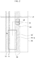
FIG. 2 is a partial layout view illustrating an organic light emitting diode display according to an exemplary embodiment of the present invention; -
FIG. 3 is a cross-sectional view taken along a line III-III ofFIG. 2 ; -
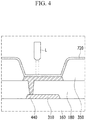
FIG. 4 andFIG. 5 are views illustrating a comparative example explaining a process in which an auxiliary member of a region A ofFIG. 3 is damaged; -
FIG. 6 is a view illustrating an exemplary variation of an organic light emitting diode display ofFIG. 3 ; and -
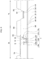
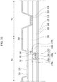
FIG. 7 to FIG. 12 are views sequentially illustrating a method of manufacturing an organic light emitting diode display according to an exemplary embodiment of the present invention. - Exemplary embodiments of the present invention will be described more fully hereinafter with reference to the accompanying drawings. As those skilled in the art would realize, the described embodiments may be modified in various different ways, all without departing from the scope of the present disclosure. The drawings and description are to be regarded as illustrative in nature. Like reference numerals may designate like elements throughout the specification.
- In the drawings, the thicknesses of layers, films, panels, regions, areas, etc., may be exaggerated for clarity. It will be understood that when an element such as a layer, film, region, or substrate is referred to as being "on" another element, it can be directly on the other element or intervening elements may also be present.
- Also, the present invention is not limited to the number of thin film transistors (TFT) and capacitors shown in accompanying drawings, and in the organic light emitting diode display, each pixel may be provided with a plurality of transistors and at least one capacitor, and may be formed to have various structures by further forming additional wires or omitting existing wires. As defined herein, the pixel is a minimum unit for displaying an image, and the organic light emitting diode display displays the image through the plurality of pixels. In particular, the pixel may be a minimum unit for displaying any desired color, while the sub-pixel may be a minimum unit for displaying a particular single color.
- An organic light emitting diode display according to an exemplary embodiment of the present invention will be described below with reference to
FIG. 1 to FIG. 3 . - The organic light emitting diode display according to an exemplary embodiment of the present invention may be made of a plurality of pixels each including a plurality of sub-pixels. Each sub-pixel can display a primary color such as red, green, blue, etc., and a predetermined color may be realized in one pixel by a combination of a plurality of sub-pixels representing these colors.
- Referring to
FIG. 2 andFIG. 3 , at least one sub-pixel may include a display area DA emitting light and a peripheral area PA adjacent to the display area DA. According to an exemplary embodiment of the present invention, light is emitted from anorganic emission layer 720 disposed between afirst electrode 710 and asecond electrode 730 in the display area DA, and a common voltage may be transmitted to thesecond electrode 730 through anauxiliary electrode 310 disposed in the peripheral area PA. - According to an exemplary embodiment of the present invention, at least one sub-pixel among a plurality of sub-pixels of one pixel may include the peripheral area PA. For example, when the plurality of sub-pixels are respectively a red sub-pixel, a green sub-pixel, and a blue sub-pixel, only the red sub-pixel may include both the display area DA and the peripheral area PA, while the green sub-pixel and the blue sub-pixel may each only include the display area DA. The common voltage supplied through the red sub-pixel may be commonly used in the green sub-pixel and the blue sub-pixel.
- However, the present invention is not limited to this particular arrangement, and the red sub-pixel, the green sub-pixel, and the blue sub-pixel may all include the display area DA and the peripheral area PA. The common voltage is respectively supplied to the red, green, and blue sub-pixels.
- A principal of operation of one sub-pixel of the organic light emitting diode display will be described below with reference to
FIG. 1 . -
FIG. 1 is an equivalent circuit diagram illustrating one pixel of an organic light emitting diode display according to an exemplary embodiment of the present invention. - As shown in
FIG. 1 , in the organic light emitting diode display according to an exemplary embodiment of the present invention, one sub-pixel PX includes a plurality ofsignal lines - The plurality of transistors Td, Ts, and Tvth include a driving transistor Td, a switching transistor Ts, and a compensation transistor Tvth. The plurality of capacitors Cst and Cvth includes a storage capacitor Cst and a compensation capacitor Cvth.
- The signal lines 121, 122, 171, 172 includes a
gate line 121 transmitting a scan signal Sn, acompensation control line 122 transmitting a compensation control signal Gc to the compensation transistor Tvth, adata line 171 crossing thegate line 121 and transmitting a data voltage Dm, and a drivingvoltage line 172 transmitting a driving voltage ELVDD to the driving transistor Td. - A gate electrode of the driving transistor Td is connected to one terminal of the compensation capacitor Cvth, a source electrode of the driving transistor Td is connected to the driving
voltage line 172, and a drain electrode of the driving transistor Td is electrically connected to an anode of the organic light emitting diode OLED. - The compensation transistor Tvth includes a gate electrode connected to the
compensation control line 122, a source electrode connected to the drain electrode of the driving transistor Td and the anode of the organic light emitting diode OLED, and a drain electrode connected to one terminal of the compensation capacitor Cvth and the gate electrode of the driving transistor Td. The compensation transistor Tvth is turned on according to the compensation control signal Gc transmitted through thecompensation control line 122 such that the gate electrode and the drain electrode of the driving transistor Td are connected to each other, thereby diode-connecting the driving transistor Td. - A voltage corresponding to a threshold voltage of the driving thin film transistor Td is programmed in the compensation capacitor Cvth when the driving transistor Td is diode-connected.
- The gate electrode of the switching thin film transistor Ts is connected to the
gate line 121, the source electrode of the switching thin film transistor Ts is connected to thedata line 171, and the drain electrode of the switching thin film transistor Ts is connected to the other terminal of the storage capacitor Cst and the other terminal of the compensation capacitor Cvth. The switching thin film transistor Ts is turned on according to the scan signal Sn transmitted through thegate line 121. - One terminal of the storage capacitor Cst is connected to the driving
voltage line 172, and a gate-source voltage of the driving transistor Td is determined according to the programed voltage in the compensation capacitor Cvth and the storage capacitor Cst. The cathode of the organic light emitting diode OLED is connected to acommon voltage line 741 transmitting a common voltage ELVSS. - The organic light emitting diode OLED emits light according to a driving current Id transmitted through the driving transistor Td from the driving
voltage line 172, and the driving current Id flows into thecommon voltage line 741. - The present invention is not limited to the 3-transistor and 2-capacitor structure is described herein, and the number of transistors and capacitors may vary.
- A detailed structure of an organic light emitting diode display according to an exemplary embodiment of the present invention will be described below with reference to
FIG. 2 andFIG. 3 . - Referring to
FIG. 2 andFIG. 3 , asubstrate 110 may be formed as an insulating substrate including glass, quartz, ceramic, or a plastic. Thesubstrate 110 may be made of a flexible material. - Also, a
buffer layer 120 is formed on thesubstrate 110. Thebuffer layer 120 may be formed over an entire surface of thesubstrate 110 throughout the display area DA and the peripheral area PA. Thebuffer layer 120 may be formed as a single layer of a silicon nitride (SiNx), or as a dual-layer structure in which a silicon nitride (SiNx) and a silicon oxide (SiOx) are stacked. Thebuffer layer 120 may prevent permeation of undesirable components such as impurities or moisture, and may also planarize the surface of thesubstrate 110. - A switching semiconductor layer and a driving
semiconductor layer 135b may be formed on thebuffer layer 120 and may be separated from each other. Hereafter, the drivingsemiconductor layer 135b will be described. - The driving
semiconductor layer 135b may be made of a polysilicon or an oxide semiconductor. The oxide semiconductor may include an oxide based on titanium (Ti), hafnium (Hf), zirconium (Zr), aluminum (Al), tantalum (Ta), germanium (Ge), zinc (Zn), gallium (Ga), tin (Sn), indium (In) such as zinc oxide (ZnO), indium-gallium-zinc oxide (InGaZnO4), indium zinc oxide (Zn-In-O), zinc-tin oxide (Zn-Sn-O), indium gallium oxide (In-Ga-O), indium-tin oxide (In-Sn-O), indium-zirconium oxide (In-Zr-O), indium-zirconium-zinc oxide (In-Zr-Zn-O), indium-zirconium-tin oxide (In-Zr-Sn-O), indium-zirconium-gallium oxide (In-Zr-Ga-O), indium-aluminum oxide (In-Al-O), indium-zinc-aluminum oxide (In-Zn-Al-O), indium-tin-aluminum oxide (In-Sn-Al-O), indium-aluminum-gallium oxide (In-Al-Ga-O), indium-tantalum oxide (In-Ta-O), indium-tantalum-zinc oxide (In-Ta-Zn-O), indium-tantalum-tin oxide (In-Ta-Sn-O), indium-tantalum-gallium oxide (In-Ta-Ga-O), indium-germanium oxide (In-Ge-O), indium-germanium-zinc oxide (In-Ge-Zn-O), indium-germanium-tin oxide (In-Ge-Sn-O), indium-germanium gallium oxide (In-Ge-Ga-O), titanium-indium-zinc oxide (Ti-In-Zn-O), and/or hafnium-indium-zinc oxide (Hf-In-Zn-O) which are complex oxides thereof. - When the driving
semiconductor layer 135b is made of the oxide semiconductor, to protect the oxide semiconductor that is vulnerable to an external environment such as a high temperature, a separate passivation layer may be added. - The driving
semiconductor layer 135b includes a channel area in which impurities are not doped, and a source area and a drain area in which impurities are doped at respective sides of the channel area. The impurities used may be selected according to a kind of thin film transistor being used, and may be, for example, N-type impurities or P-type impurities. - The driving
semiconductor layer 135b is divided into achannel region 1355, asource region 1356, and adrain region 1357. Thesource region 1356 and thedrain region 1357 are respectively formed at opposite sides of thechannel region 1355. - The
channel region 1355 of the drivingsemiconductor layer 135b may include polycrystalline silicon in which no impurity is doped (an intrinsic semiconductor). - The
source region 1356 and thedrain region 1357 of the drivingsemiconductor layer 135b may include polycrystalline silicon in which a conductive impurity is doped (an impurity semiconductor). - A
gate insulating layer 140 is formed on the drivingsemiconductor layer 135b. Thegate insulating layer 140 may be a single layer or a multilayer including at least one of a silicon nitride and a silicon oxide. - A driving
gate electrode 125b is formed on thegate insulating layer 140. - The driving
gate electrode 125b may be disposed on the drivingsemiconductor layer 135b. The drivinggate electrode 125b may at least partially overlap thechannel region 1355. - An interlayer insulating
layer 160 is formed on the drivinggate electrode 125b. The interlayer insulatinglayer 160 may be made of a silicon nitride or a silicon oxide. - The interlayer insulating
layer 160 and thegate insulating layer 140 have asource contact hole 61 and adrain contact hole 62 respectively exposing thesource region 1356 and thedrain region 1357. A drivingsource electrode 176b and a drivingdrain electrode 177b are formed on theinterlayer insulating layer 160. - The driving
source electrode 176b is connected to thesource region 1356 through thesource contact hole 61. The drivingdrain electrode 177b faces the drivingsource electrode 176b. - The driving
drain electrode 177b is connected to thedrain region 1357 through thedrain contact hole 62. - The driving
semiconductor layer 135b, the drivinggate electrode 125b, the drivingsource electrode 176b, and the drivingdrain electrode 177b form a driving thin film transistor T. - The driving thin film transistor T corresponds to a switching element. According to an exemplary embodiment of the present invention, the driving thin film transistor T may be formed in each sub-pixel of the organic light emitting diode display.
- A
planarization layer 180 is formed on the drivingsource electrode 176b and the drivingdrain electrode 177b. Theplanarization layer 180 serves to planarize a step and to thereby increase emission efficiency of the organic light emitting element that will be formed thereon. - The
planarization layer 180 may be made of a polyacrylate resin, an epoxy resin, a phenolic resin, a polyamide resin, a polyimide resin, an unsaturated polyester resin, a polyphenylene ether resin, a polyphenylene sulfide resin, and/or benzocyclobutene (BCB). Theplanarization layer 180 may be an insulating layer. - As described above, the sub-pixel PX includes the display area DA and the peripheral area PA, and the display area DA may include the
first electrode 710, theorganic emission layer 720, and thesecond electrode 730 so as to emit light. - A first electrode, e.g. a
pixel electrode 710, is formed on theplanarization layer 180. Thepixel electrode 710 may be formed of a transparent conductive material such as indium tin oxide (ITO), indium zinc oxide (IZO), zinc oxide (ZnO), or indium oxide (In2O3), or a reflective metal such as lithium (Li), calcium (Ca), lithium fluoride/calcium (LiF/Ca), lithium fluoride/aluminum (LiF/Al), aluminum (Al), silver (Ag), magnesium (Mg), or gold (Au). For example, thepixel electrode 710 may be formed by sequentially stacking ITO, Ag, and ITO. - The
pixel electrode 710 is electrically connected to the drivingdrain electrode 177b of the thin film transistor T through acontact hole 181 formed in theplanarization layer 180, thereby constituting the anode of the organiclight emitting element 70. - A
pixel definition layer 350 is formed on theplanarization layer 180 and an edge of thepixel electrode 710. Thepixel definition layer 350 has afourth opening 352 exposing thepixel electrode 710. Thepixel definition layer 350 may also have athird opening 351 exposing a part of anauxiliary member 410, which is described in greater detail below. - The
pixel definition layer 350 may be made of a resin such as a polyacrylate resin and a polyimide resin, a silica-based inorganic material, or the like. - An
organic emission layer 720 is formed in thefourth opening 352 of thepixel definition layer 350. Theorganic emission layer 720 is formed on thefirst electrode 710 exposed in the display area DA and also extends to the peripheral area PA. As shown inFIG. 3 , theorganic emission layer 720 is also disposed in thethird opening 351 of thepixel definition layer 350. - The
organic emission layer 720 has a multilayer structure including an emission layer and a hole-injection layer (HIL), a hole-transporting layer (HTL), electron-transporting layer (ETL), and/or an electron-injection layer (EIL). - When the
organic emission layer 720 includes all of the above-mentioned layers, the hole injection layer may be disposed on thepixel electrode 710 to correspond to an anode, and the hole transporting layer, the emission layer, the electron transporting layer, and the electron injection layer may be sequentially stacked thereon. - The
organic emission layer 720 may include a red emitting layer emitting red light, a green emitting layer emitting green light, and a blue emitting layer emitting blue light. The red emitting layer, the green emitting layer, and the blue emitting layer are respectively formed on a red pixel, a green pixel, and a blue pixel to implement a color image. - A second electrode (common electrode) 730, is formed on the
pixel definition layer 350 and theorganic emission layer 720. Thecommon electrode 730 is formed as a single structure across the plurality of sub-pixels. For example, thecommon electrode 730 may be formed continuously throughout the red sub-pixel, the green sub-pixel, and the blue sub-pixel. - In addition, according to an exemplary embodiment of the present invention, the
common electrode 730 extends to the peripheral area PA as well as the display area DA. Accordingly, thecommon electrode 730 may be disposed on theorganic emission layer 720 within the peripheral area PA. - The
common electrode 730 may include a transparent conductive material such as indium tin oxide (ITO), indium zinc oxide (IZO), zinc oxide (ZnO), or indium oxide (In2O3), or a reflective metal such as lithium (Li), calcium (Ca), lithium fluoride/calcium (LiF/Ca), lithium fluoride/aluminum (LiF/Al), aluminum (Al), silver (Ag), magnesium (Mg), or gold (Au). - The
common electrode 730 acts as the cathode of the organiclight emitting element 70. As described above, thepixel electrode 710, theorganic emission layer 720, and thecommon electrode 730 form the organiclight emitting element 70. - In the peripheral area PA of the sub-pixel PX, the
auxiliary electrode 310 may be disposed on theinterlayer insulating layer 160. Theauxiliary electrode 310 transmits a common voltage ELVSS to thecommon electrode 730. Theauxiliary electrode 310 may correspond to a common voltage line transmitting the common voltage ELVSS. - The
auxiliary electrode 310 may be exposed by afirst opening 182 formed in theplanarization layer 180. A part of an upper surface of theauxiliary electrode 310 may be exposed by thefirst opening 182. - A cross-sectional shape of the
first opening 182 may be rectangular. - Accordingly, the
auxiliary electrode 310 may also be exposed with the rectangular shape. - The
auxiliary electrode 310 may be formed of the same layer as the above-describeddriving source electrode 176b and drivingdrain electrode 177b. For example, theauxiliary electrode 310, the drivingsource electrode 176b, and the drivingdrain electrode 177b may be formed by forming and patterning the same metal layer on theinterlayer insulating layer 160. - The
auxiliary electrode 310 may have a multilayer structure in which metal layers including copper (Cu), copper alloys, aluminum (Al), aluminum alloys, molybdenum (Mo), and molybdenum alloys are stacked. For example, theauxiliary electrode 310 may have a triple-layer structure including titanium/aluminum/titanium (Ti/Al/Ti), molybdenum/aluminum/molybdenum (Mo/Al/Mo), or molybdenum/copper/molybdenum (Mo/Cu/Mo). - According to an exemplary embodiment of the present invention, an
auxiliary member 410 that is in contact with theauxiliary electrode 310 is disposed on theauxiliary electrode 310. Theauxiliary member 410 is in contact with theauxiliary electrode 310, thereby transmitting the common voltage ELVSS through theauxiliary electrode 310 to thecommon electrode 730. - The
auxiliary member 410 is in contact with the entire upper surface of theauxiliary electrode 310 exposed in thefirst opening 182. For example, to not expose theplanarization layer 180 between theauxiliary electrode 310 and theauxiliary member 410, theauxiliary member 410 covers the entire upper surface of theauxiliary electrode 310. - According to an exemplary embodiment of the present invention, the
auxiliary member 410 is only disposed within thefirst opening 182 of theplanarization layer 180. Theauxiliary member 410 is in contact with a part of an interior circumference of thefirst opening 182. For example, part of theauxiliary member 410 is not disposed at the upper surface of theplanarization layer 180. - Referring to
FIG. 4 andFIG. 5 , if theplanarization layer 180 is formed between anauxiliary member 440 and theauxiliary electrode 310, in the process of forming asecond opening 721 in theorganic emission layer 720 by using a laser L, theauxiliary member 440 may be damaged. - For example, when the
auxiliary member 440 is made of anfirst ITO layer 441, aAg layer 442, and asecond ITO layer 443, while theauxiliary member 440 is bent to the side of theplanarization layer 180 by the laser L, thefirst ITO layer 441, theAg layer 442, and thesecond ITO layer 443 may each be cut (F). Accordingly, while the remaining gas component in theplanarization layer 180 of the organic layer is discharged through the cut region (F), thecommon electrode 730 may be oxidized. If thecommon electrode 730 is oxidized, theorganic emission layer 720 might not emit light. - Referring to
FIG. 3 , according to an exemplary embodiment of the present invention, as theauxiliary member 410 is disposed to be in contact with the exposed entire upper surface of theauxiliary electrode 310, theauxiliary member 410 may be prevented from being bent in the lower direction and damaged by the laser L. Accordingly, the oxidization of thecommon electrode 730 is prevented and generation of a dark spot of the organic light emitting diode display due to lack of emission of theorganic emission layer 720 may be prevented. - The
auxiliary electrode 310 of the metal material disposed under theauxiliary member 410 serves to support theauxiliary member 410. - As the
auxiliary member 410 is in contact with the entire upper surface of theauxiliary electrode 310, a contact area of theauxiliary member 410 and theauxiliary electrode 310 increases such that resistance of the wire to which the common voltage is transmitted may be reduced. Accordingly, in the organic light emitting diode display, the voltage drop (IR-Drop) may be prevented and accordingly, the luminance may remain uniform. - The
auxiliary member 410 may be formed of the same layer as thefirst electrode 710. Theauxiliary member 410 may be made of a transparent conductive material such as indium tin oxide (ITO), indium zinc oxide (IZO), zinc oxide (ZnO), or indium oxide (In2O3), or a reflective metal such as lithium (Li), calcium (Ca), lithium fluoride/calcium (LiF/Ca), lithium fluoride/aluminum (LiF/Al), aluminum (Al), silver (Ag), magnesium (Mg), or gold (Au). For example, theauxiliary member 410 may be formed by sequentially stacking ITO, Ag, and ITO. - In
FIG. 3 , theauxiliary member 440 is disposed within thefirst opening 182, however part of an auxiliary member may be disposed at the upper surface of theplanarization layer 180. As shown inFIG. 6 , theauxiliary member 420 fills thefirst opening 182 of theplanarization layer 180, and a part thereof may be disposed at the upper surface of theplanarization layer 180. - According to an exemplary embodiment of the present invention, the
organic emission layer 720 is disposed on theauxiliary member 410 in the peripheral area PA. In theorganic emission layer 720, asecond opening 721 exposing part of the underlyingauxiliary member 410 is formed. Thesecond opening 721 of theorganic emission layer 720 is formed by the laser L. After theorganic emission layer 720 is coated on theauxiliary member 410, theorganic emission layer 720 is irradiated by the laser L in the region where theauxiliary member 410 and theauxiliary electrode 310 are overlapped with each other. - By the laser L, the
second opening 721 is formed in theorganic emission layer 720. The cross-sectional shape of thesecond opening 721 may be circular. - A diameter H2 of the
second opening 721 may be smaller than a width H1 of thefirst opening 182. However, the present invention is not limited to this particular structure, and the diameter H2 of thesecond opening 721 may be formed to be equal to the width H1 of thefirst opening 182. If the diameter H2 of thesecond opening 721 increases, the contact area of theauxiliary member 410 and the overlyingsecond electrode 730 may increase. As described above, if the contact area increases, the resistance of the wire transmitting the common voltage may be reduced. - In the peripheral area PA, a
second electrode 730 may be formed on theorganic emission layer 720. Thesecond electrode 730 may be in contact with theauxiliary member 410 through thesecond opening 721. Accordingly, thesecond electrode 730 may be electrically connected to theauxiliary member 410 and theauxiliary electrode 310. Therefore, the common voltage ELVSS supplied through theauxiliary electrode 310 may be supplied to thesecond electrode 730 through theauxiliary member 410. - Hereinafter, a method of manufacturing the organic light emitting diode display according to an exemplary embodiment of the present invention will be described. When describing the manufacturing method of the organic light emitting diode display device according to an exemplary embodiment of the present invention, it may be understood that like elements may be similar to or identical to corresponding elements that were already described, and accordingly, repeated description of these elements may be omitted.
- First, as shown in
FIG. 7 , a thin film transistor T is formed on asubstrate 110. The thin film transistor T may be the switching thin film transistor or the driving thin film transistor. - The thin film transistor T includes a
semiconductor layer 135b, agate electrode 125b, asource electrode 176b, and adrain electrode 177b. Thegate electrode 125b is spaced apart from thesemiconductor layer 135b. Thesource electrode 176b and thedrain electrode 177b are disposed above thegate electrode 125b. - An
auxiliary electrode 310 is simultaneously formed with thesource electrode 176b and thedrain electrode 177b. After coating the metal layer on theinterlayer insulating layer 160, a photolithography process is performed on the metal layer to form theauxiliary electrode 310, and to divide thesource electrode 176b and thedrain electrode 177b. - Next, a
planarization layer 180 is formed on thesource electrode 176b anddrain electrode 177b, and theauxiliary electrode 310. - Also, referring to
FIG. 8 , by the patterning process, afirst opening 182 exposing part of theauxiliary electrode 310 and acontact hole 181 exposing part of thedrain electrode 177b are formed in theplanarization layer 180. - The cross-sectional shape of the
first opening 182 may be rectangular. - Accordingly, the exposed
auxiliary electrode 310 may be exposed with the rectangular shape. - Next, a
first electrode 710 and anauxiliary member 410 are formed on theplanarization layer 180, thereby thefirst electrode 710 is in contact with thedrain electrode 177b and theauxiliary member 410 is in contact with theauxiliary electrode 310. Theauxiliary member 410 is in contact with the entire upper surface of theauxiliary electrode 310 exposed by thefirst opening 182. - The
first electrode 710 and theauxiliary member 410 are formed with the same layer. For example, after the same metal layer is formed on theplanarization layer 180, the photolithography process is performed on the metal layer to form thefirst electrode 710 and to divide theauxiliary member 410. - Next, as shown in
FIG. 9 , apixel definition layer 350 is formed on theplanarization layer 180. In thepixel definition layer 350, athird opening 351 exposing part of theauxiliary member 410 and afourth opening 352 exposing part of thefirst electrode 710 are formed. - Next, an
organic emission layer 720 is coated on thepixel definition layer 350. Referring toFIG. 10 , theorganic emission layer 720 is formed in the display area DA and the peripheral area PA. Theorganic emission layer 720 is disposed inside thethird opening 351 and thefourth opening 352 of thepixel definition layer 350 to cover theauxiliary member 410 and thefirst electrode 710, respectively. - According to an exemplary embodiment of the present invention, after coating the
organic emission layer 720, part of theorganic emission layer 720 is removed to expose part of theauxiliary member 410 in the peripheral area PA. If part of theorganic emission layer 720 is removed, asecond opening 721 is formed in theorganic emission layer 720. - Referring to
FIG. 11 , part of theorganic emission layer 720 is removed by using the laser L to form thesecond opening 721. After the laser L is positioned at a center part of the region where theauxiliary member 410 and theauxiliary electrode 310 are overlapped, theorganic emission layer 720 is irradiated by the laser L. Thesecond opening 721 formed in theorganic emission layer 720 may be made with a circular shape by the laser L. - As described above, as the
auxiliary electrode 310 is disposed to be in contact under theauxiliary member 410, theauxiliary member 410 might not be bent down and damaged by the laser L. - Next, the
second electrode 730 is formed on theorganic emission layer 720. Thesecond electrode 730 may be in contact with theauxiliary member 410 through thesecond opening 721. Accordingly, thesecond electrode 730 may be electrically connected to theauxiliary member 410 and theauxiliary electrode 310. Therefore, the common voltage ELVSS supplied through theauxiliary electrode 310 may be supplied to thesecond electrode 730 through theauxiliary member 410. - In the organic light emitting diode display and the method of manufacturing the OLED display, according to an exemplary embodiment of the present invention, in the process of removing part of the
organic emission layer 720 by using the laser L, theauxiliary member 410 may be prevented from being damaged by the laser L. Additionally, thecommon electrode 730 may be prevented from being oxidized as remaining gas component of the organic layer is prevented from being discharged along a gap of a damagedauxiliary member 410. - While this invention has been described in connection with what is presently considered to be practical exemplary embodiments, it is to be understood that the invention is not limited to the disclosed embodiments, but, on the contrary, is intended to cover various modifications and equivalent arrangements included within the scope of the present disclosure as defined in the claims.
Claims (20)
- An organic light emitting diode display comprising:a substrate (110);a pixel formed on the substrate (110) and including a display area (DA) displaying an image and a peripheral area (PA) adjacent to the display area (DA);an insulating layer at the display area (DA) and the peripheral area (PA) on the substrate (110);a first electrode (710) at the display area (DA) on the insulating layer;an organic emission layer (720) on the first electrode (710) and extending to the peripheral area (PA);a second electrode (730) on the organic emission layer (720) and disposed in the display area (DA) and the peripheral area (PA);an auxiliary electrode (310) in the peripheral area (PA) on the substrate (110) and partially exposed by a first opening formed (182) in the insulating layer; andan auxiliary member (410, 420) on the auxiliary electrode (310) and in contact with an upper surface of the auxiliary electrode (310) exposed by the first opening (182).
- The organic light emitting diode display of claim 1, wherein
the auxiliary member (410, 420) is entirely in contact with the upper surface of the auxiliary electrode (310). - The organic light emitting diode display of claim 1 or 2, wherein
the organic emission layer (720) is disposed on the auxiliary member (410, 420) in the peripheral area (PA) and has a second opening (721) exposing part of the auxiliary member (410, 420). - The organic light emitting diode display of claim 3, wherein
the second electrode (730) is in contact with the auxiliary member (410, 420) through the second opening (721). - The organic light emitting diode display of claim 3 or 4, wherein the second opening (721) has a circular shape.
- The organic light emitting diode display of at least one of claims 1 to 5, wherein
the auxiliary member (410, 420) covers the first opening (182) of the insulating layer. - The organic light emitting diode display of at least one of claims 1 to 6, wherein
the auxiliary member (420) is in contact with a part of an interior circumference of the first opening (182). - The organic light emitting diode display of at least one of claims 1 to 7, wherein
the auxiliary member (410, 420) is formed with the same layer as the first electrode (710). - The organic light emitting diode display of at least one of claims 1 to 8, wherein
the auxiliary member (410, 420) is formed by sequentially stacking ITO (indium tin oxide), silver (Ag), and ITO. - The organic light emitting diode display of at least one of claims 1 to 9, wherein
the auxiliary electrode (310) is a common voltage line (741) transmitting a common voltage. - The organic light emitting diode display of at least one of claims 1 to 10, wherein
the auxiliary electrode (310) is formed by sequentially stacking molybdenum (Mo), aluminum (Al), and molybdenum (Mo). - The organic light emitting diode display of at least one of claims 1 to 11, wherein
the pixel includes at least one sub-pixel (PX) including the display area (DA) and the peripheral area (PA), and
the sub-pixel (PX) is a red sub-pixel (PX). - A method for manufacturing an organic light emitting diode display, comprising:preparing a substrate (110);forming a thin film transistor (T) including a semiconductor layer (135b), a gate electrode (125b) on the semiconductor layer (135b), and a source electrode (176b) and a drain electrode (177b) connected to the semiconductor layer (135b) on the substrate (110);forming an auxiliary electrode (310) supplying a common voltage on the substrate (110);forming an insulating layer on the thin film transistor (T) and the auxiliary electrode (310) and exposing parts of the drain electrode (177b) and the auxiliary electrode (310);forming a first electrode (710) on the insulating layer and in contact with the drain electrode (177b);forming an auxiliary member (410, 420) in contact with the auxiliary electrode (310) through a first opening (182) formed in the insulating layer;forming an organic emission layer (720) on the first electrode (710) and the auxiliary member (410, 420);removing a part of the organic emission layer (720) to expose a part of the auxiliary member (410, 420); andforming a second electrode (730) on the organic emission layer (720).
- The method of claim 13, wherein
the removing of the part of the organic emission layer (720) is performed by using a laser (L). - The method of claim 13 or 14, wherein
the removing of the part of the organic emission layer (720) includes forming a second opening (721) by removing the part of the organic emission layer (720). - The method of claim 15, wherein
the second opening (721) has a circular shape. - The method of at least one of claims 13 to 15, further comprising
forming a pixel definition layer (350) having a third opening (351) exposing the part of the auxiliary member (410, 420) and a fourth opening (352) exposing the part of the first electrode (710). - The method of at least one of claims 13 to 17, wherein:the source electrode (176b), the drain electrode (177b), and the auxiliary electrode (310) are formed with the same layer.
- The method of at least one of claims 13 to 18, wherein
the first electrode (710) and the auxiliary member (410, 420) are formed with the same layer. - The method of at least one of claims 13 to 19, wherein
the auxiliary member (410, 420) is in contact with an entire upper surface of the auxiliary electrode (310) exposed by the first opening (182).
Applications Claiming Priority (1)
| Application Number | Priority Date | Filing Date | Title |
|---|---|---|---|
| KR1020160165997A KR102823585B1 (en) | 2016-12-07 | 2016-12-07 | Organic light emitting diode display and manufacturing method thereof |
Publications (2)
| Publication Number | Publication Date |
|---|---|
| EP3333924A1 true EP3333924A1 (en) | 2018-06-13 |
| EP3333924B1 EP3333924B1 (en) | 2025-08-13 |
Family
ID=60627458
Family Applications (1)
| Application Number | Title | Priority Date | Filing Date |
|---|---|---|---|
| EP17205586.5A Active EP3333924B1 (en) | 2016-12-07 | 2017-12-06 | Organic light emitting diode display and method of manufacturing the same |
Country Status (5)
| Country | Link |
|---|---|
| US (2) | US10147769B2 (en) |
| EP (1) | EP3333924B1 (en) |
| JP (1) | JP7249098B2 (en) |
| KR (1) | KR102823585B1 (en) |
| CN (1) | CN108172597B (en) |
Cited By (2)
| Publication number | Priority date | Publication date | Assignee | Title |
|---|---|---|---|---|
| EP3712951A1 (en) * | 2019-03-20 | 2020-09-23 | Samsung Display Co., Ltd. | Display apparatus and method of manufacturing the same |
| EP4170726A1 (en) * | 2021-10-22 | 2023-04-26 | Samsung Display Co., Ltd. | Display device and manufacturing method thereof |
Families Citing this family (57)
| Publication number | Priority date | Publication date | Assignee | Title |
|---|---|---|---|---|
| CA3002752A1 (en) | 2015-10-26 | 2017-05-04 | Oti Lumionics Inc. | Method for patterning a coating on a surface and device including a patterned coating |
| KR102802931B1 (en) | 2016-12-02 | 2025-05-08 | 오티아이 루미오닉스 인크. | Device including a conductive coating disposed over emissive regions and method therefor |
| KR102823585B1 (en) | 2016-12-07 | 2025-06-20 | 삼성디스플레이 주식회사 | Organic light emitting diode display and manufacturing method thereof |
| KR102563713B1 (en) | 2017-04-26 | 2023-08-07 | 오티아이 루미오닉스 인크. | Methods of patterning the coating of a surface and apparatus comprising the patterned coating |
| CN110832660B (en) | 2017-05-17 | 2023-07-28 | Oti照明公司 | Method of selectively depositing a conductive coating on a patterned coating and an apparatus comprising the conductive coating |
| CN107394060B (en) * | 2017-09-07 | 2024-01-19 | 京东方科技集团股份有限公司 | Display panel, display device and method of preparing display panel |
| US11751415B2 (en) | 2018-02-02 | 2023-09-05 | Oti Lumionics Inc. | Materials for forming a nucleation-inhibiting coating and devices incorporating same |
| US11489136B2 (en) | 2018-05-07 | 2022-11-01 | Oti Lumionics Inc. | Method for providing an auxiliary electrode and device including an auxiliary electrode |
| CN108831302B (en) * | 2018-06-19 | 2020-08-21 | 武汉天马微电子有限公司 | Display panel and display device |
| JP7108478B2 (en) * | 2018-06-21 | 2022-07-28 | 株式会社ジャパンディスプレイ | Display device |
| KR102585158B1 (en) * | 2018-07-04 | 2023-10-05 | 삼성디스플레이 주식회사 | Display device |
| KR102554738B1 (en) * | 2018-07-17 | 2023-07-11 | 엘지디스플레이 주식회사 | Organic light emitting diode device and favricating method thereof |
| JP2022508040A (en) | 2018-11-23 | 2022-01-19 | オーティーアイ ルミオニクス インコーポレーテッド | Optoelectronic device containing light transmission region |
| KR102719960B1 (en) | 2018-12-27 | 2024-10-18 | 엘지디스플레이 주식회사 | Organic light emitting display apparatus |
| US12021070B2 (en) | 2018-12-28 | 2024-06-25 | Honor Device Co., Ltd. | Display, electronic device, and display fabrication method |
| KR102621016B1 (en) * | 2018-12-28 | 2024-01-05 | 삼성디스플레이 주식회사 | Organic light emitting display device and method of manufacturing organic light emitting display device |
| KR20250160226A (en) | 2019-03-07 | 2025-11-11 | 오티아이 루미오닉스 인크. | Materials for forming a nucleation-inhibiting coating and devices incorporating same |
| US11963384B2 (en) * | 2019-03-26 | 2024-04-16 | Sharp Kabushiki Kaisha | Display device and method for manufacturing same |
| US12219797B2 (en) * | 2019-03-26 | 2025-02-04 | Sharp Kabushiki Kaisha | Display device including a frame-like shape oxide semiconductor layer |
| JP7555600B2 (en) | 2019-04-18 | 2024-09-25 | オーティーアイ ルミオニクス インコーポレーテッド | Materials for forming nucleation-inhibiting coatings and devices incorporating same - Patents.com |
| JP7576337B2 (en) | 2019-05-08 | 2024-11-01 | オーティーアイ ルミオニクス インコーポレーテッド | Materials for forming nucleation-inhibiting coatings and devices incorporating same - Patents.com |
| CN110224005B (en) * | 2019-05-10 | 2021-04-02 | 深圳市华星光电半导体显示技术有限公司 | Display and preparation method thereof |
| KR102698884B1 (en) * | 2019-05-13 | 2024-08-28 | 삼성디스플레이 주식회사 | Display apparatus and method of manufacturing the same |
| US10991682B2 (en) * | 2019-05-29 | 2021-04-27 | Innolux Corporation | Electronic device |
| US11832473B2 (en) | 2019-06-26 | 2023-11-28 | Oti Lumionics Inc. | Optoelectronic device including light transmissive regions, with light diffraction characteristics |
| KR20240134240A (en) | 2019-06-26 | 2024-09-06 | 오티아이 루미오닉스 인크. | Optoelectronic device including light transmissive regions with light diffraction characteristics |
| CN110350008A (en) * | 2019-07-02 | 2019-10-18 | 深圳市华星光电半导体显示技术有限公司 | Preparation method, luminescent panel and the display device of luminescent panel |
| KR102818817B1 (en) | 2019-08-09 | 2025-06-11 | 오티아이 루미오닉스 인크. | Optoelectronic device including auxiliary electrode and partition |
| CN110579913B (en) * | 2019-08-09 | 2020-12-04 | 武汉华星光电半导体显示技术有限公司 | Display panel and display device |
| CN110854290B (en) * | 2019-10-29 | 2021-06-22 | 苏州华星光电技术有限公司 | A display panel and its manufacturing method |
| KR102888824B1 (en) * | 2019-11-12 | 2025-11-21 | 삼성디스플레이 주식회사 | Display device and method of manufacturing display device |
| CN115552643B (en) | 2019-12-24 | 2025-08-19 | Oti照明公司 | Light emitting device including cover layer and method of manufacturing the same |
| KR102687966B1 (en) * | 2019-12-30 | 2024-07-23 | 엘지디스플레이 주식회사 | Display device |
| KR102792575B1 (en) * | 2020-02-11 | 2025-04-09 | 삼성디스플레이 주식회사 | Display apparatus and manufacturing the same |
| KR20210116764A (en) * | 2020-03-13 | 2021-09-28 | 삼성디스플레이 주식회사 | Manufacturing method of display apparatus |
| US11997891B2 (en) | 2020-03-24 | 2024-05-28 | Boe Technology Group Co., Ltd. | Display substrate, fabricating method thereof and display panel |
| CN111525042A (en) * | 2020-04-26 | 2020-08-11 | 深圳市华星光电半导体显示技术有限公司 | Organic light emitting diode display panel and manufacturing method thereof |
| KR102930123B1 (en) * | 2020-05-26 | 2026-02-24 | 삼성디스플레이 주식회사 | Display device |
| KR102956640B1 (en) * | 2020-08-06 | 2026-04-23 | 삼성디스플레이 주식회사 | Display panel and display apparatus including the same |
| CN112038357B (en) * | 2020-08-31 | 2024-10-01 | 武汉天马微电子有限公司 | Display panel, display device and manufacturing method |
| KR20220056924A (en) * | 2020-10-28 | 2022-05-09 | 삼성디스플레이 주식회사 | Display device |
| KR20220075071A (en) * | 2020-11-27 | 2022-06-07 | 삼성디스플레이 주식회사 | Display apparatus and method for inspecting defect of display apparatus |
| CN114582928A (en) | 2020-11-30 | 2022-06-03 | 乐金显示有限公司 | Electroluminescent display device |
| US11985841B2 (en) | 2020-12-07 | 2024-05-14 | Oti Lumionics Inc. | Patterning a conductive deposited layer using a nucleation inhibiting coating and an underlying metallic coating |
| KR20220090032A (en) * | 2020-12-22 | 2022-06-29 | 엘지디스플레이 주식회사 | Electroluminesence display |
| KR102847530B1 (en) * | 2021-01-15 | 2025-08-19 | 삼성디스플레이 주식회사 | Display device and method of manufacturing the same |
| US12238969B2 (en) | 2021-02-26 | 2025-02-25 | Hefei Xinsheng Optoelectronics Technology Co., Ltd. | Display substrate, method for manufacturing the same, and display device |
| KR20220168616A (en) | 2021-06-16 | 2022-12-26 | 삼성디스플레이 주식회사 | Display device and manufacturing method thereof |
| KR20230058200A (en) | 2021-10-22 | 2023-05-03 | 삼성디스플레이 주식회사 | Display panel, electronic apparatus including the same and method of manufacturing display panel |
| CN114141841B (en) * | 2021-11-26 | 2025-03-28 | 合肥京东方卓印科技有限公司 | Display substrate and manufacturing method thereof, and display device |
| KR102896742B1 (en) * | 2021-12-13 | 2025-12-05 | 삼성디스플레이 주식회사 | Display device and method for manufacturing the same |
| KR102851043B1 (en) * | 2021-12-29 | 2025-08-27 | 엘지디스플레이 주식회사 | Display Apparatus having a light-emitting device |
| KR20230100956A (en) * | 2021-12-29 | 2023-07-06 | 엘지디스플레이 주식회사 | Display device and manufacturing method thereof |
| TWI808759B (en) | 2022-05-13 | 2023-07-11 | 天光材料科技股份有限公司 | Electrode connection structure and method of forming the same |
| KR20250040567A (en) | 2022-07-29 | 2025-03-24 | 보에 테크놀로지 그룹 컴퍼니 리미티드 | Display substrate and its manufacturing method, display device |
| WO2024113296A1 (en) * | 2022-12-01 | 2024-06-06 | 京东方科技集团股份有限公司 | Light-emitting substrate, display panel, and display device |
| CN117042510A (en) * | 2023-06-30 | 2023-11-10 | 京东方科技集团股份有限公司 | Display panel, preparation method and display device thereof |
Citations (6)
| Publication number | Priority date | Publication date | Assignee | Title |
|---|---|---|---|---|
| EP1489671A2 (en) * | 2003-06-16 | 2004-12-22 | Eastman Kodak Company | Method of making a top-emitting oled device having improved power distribution |
| US20070048886A1 (en) * | 2005-08-29 | 2007-03-01 | Eastman Kodak Company | Electrical connection in OLED devices |
| US20070080356A1 (en) * | 2005-08-17 | 2007-04-12 | Sony Corporation | Display device and method for manufacturing display device |
| US20140239262A1 (en) * | 2013-02-25 | 2014-08-28 | Samsung Display Co., Ltd. | Organic light-emitting display device and method of manufacturing the same |
| US20140374732A1 (en) * | 2013-05-31 | 2014-12-25 | Samsung Display Co., Ltd. | Organic light emitting display apparatus and method of manufacturing the same |
| US20160293888A1 (en) * | 2015-04-02 | 2016-10-06 | Lg Display Co., Ltd. | Auxiliary Lines Reducing Resistance In A Cathode Of An Organic Light Emitting Display Device |
Family Cites Families (12)
| Publication number | Priority date | Publication date | Assignee | Title |
|---|---|---|---|---|
| GB2403101B (en) | 2003-06-18 | 2005-12-21 | Matsushita Electric Industrial Co Ltd | Extended dynamic resource allocation in packet data transfer |
| KR100546663B1 (en) | 2003-08-05 | 2006-01-26 | 엘지전자 주식회사 | Top-Emission Organic EL Device and Manufacturing Method Thereof |
| US20070048386A1 (en) | 2005-08-30 | 2007-03-01 | Mallozzi Ottavio Sr | Medicament for treating inflammatory and non-inflammatory arthritis |
| KR100736576B1 (en) | 2006-04-10 | 2007-07-06 | 엘지전자 주식회사 | Electroluminescent element and manufacturing method |
| KR101574211B1 (en) | 2008-09-05 | 2015-12-07 | 삼성디스플레이 주식회사 | Organic light emitting diode display |
| KR101699911B1 (en) * | 2010-04-05 | 2017-01-26 | 삼성디스플레이 주식회사 | Organic light emitting diode display |
| KR101372641B1 (en) * | 2012-04-18 | 2014-03-17 | 주식회사 야스 | Method for manufacturing oled using laser burning |
| US9362345B2 (en) | 2013-05-31 | 2016-06-07 | Samsung Display Co., Ltd. | Organic light emitting display apparatus and method of manufacturing the same |
| JP2015074810A (en) | 2013-10-10 | 2015-04-20 | 日東電工株式会社 | Sputtering apparatus and method for exchanging film roll thereof |
| CN104167496B (en) | 2014-08-01 | 2018-02-23 | 上海和辉光电有限公司 | Inversion type top emitting device and preparation method thereof |
| KR102443645B1 (en) * | 2016-01-13 | 2022-09-15 | 삼성디스플레이 주식회사 | Organic light emitting diode display and manufacturing method thereof |
| KR102823585B1 (en) | 2016-12-07 | 2025-06-20 | 삼성디스플레이 주식회사 | Organic light emitting diode display and manufacturing method thereof |
-
2016
- 2016-12-07 KR KR1020160165997A patent/KR102823585B1/en active Active
-
2017
- 2017-09-21 US US15/711,103 patent/US10147769B2/en active Active
- 2017-12-06 JP JP2017234262A patent/JP7249098B2/en active Active
- 2017-12-06 EP EP17205586.5A patent/EP3333924B1/en active Active
- 2017-12-07 CN CN201711284818.0A patent/CN108172597B/en active Active
-
2018
- 2018-11-12 US US16/186,817 patent/US10446613B2/en active Active
Patent Citations (6)
| Publication number | Priority date | Publication date | Assignee | Title |
|---|---|---|---|---|
| EP1489671A2 (en) * | 2003-06-16 | 2004-12-22 | Eastman Kodak Company | Method of making a top-emitting oled device having improved power distribution |
| US20070080356A1 (en) * | 2005-08-17 | 2007-04-12 | Sony Corporation | Display device and method for manufacturing display device |
| US20070048886A1 (en) * | 2005-08-29 | 2007-03-01 | Eastman Kodak Company | Electrical connection in OLED devices |
| US20140239262A1 (en) * | 2013-02-25 | 2014-08-28 | Samsung Display Co., Ltd. | Organic light-emitting display device and method of manufacturing the same |
| US20140374732A1 (en) * | 2013-05-31 | 2014-12-25 | Samsung Display Co., Ltd. | Organic light emitting display apparatus and method of manufacturing the same |
| US20160293888A1 (en) * | 2015-04-02 | 2016-10-06 | Lg Display Co., Ltd. | Auxiliary Lines Reducing Resistance In A Cathode Of An Organic Light Emitting Display Device |
Cited By (5)
| Publication number | Priority date | Publication date | Assignee | Title |
|---|---|---|---|---|
| EP3712951A1 (en) * | 2019-03-20 | 2020-09-23 | Samsung Display Co., Ltd. | Display apparatus and method of manufacturing the same |
| US11335755B2 (en) | 2019-03-20 | 2022-05-17 | Samsung Display Co., Ltd. | Display apparatus and method of manufacturing the same |
| US12419161B2 (en) | 2019-03-20 | 2025-09-16 | Samsung Display Co., Ltd. | Display apparatus and method of manufacturing the same |
| EP4170726A1 (en) * | 2021-10-22 | 2023-04-26 | Samsung Display Co., Ltd. | Display device and manufacturing method thereof |
| US12507547B2 (en) | 2021-10-22 | 2025-12-23 | Samsung Display Co., Ltd. | Display device and manufacturing method thereof |
Also Published As
| Publication number | Publication date |
|---|---|
| CN108172597A (en) | 2018-06-15 |
| JP7249098B2 (en) | 2023-03-30 |
| US10446613B2 (en) | 2019-10-15 |
| US10147769B2 (en) | 2018-12-04 |
| CN108172597B (en) | 2023-09-12 |
| KR20180066320A (en) | 2018-06-19 |
| US20180158878A1 (en) | 2018-06-07 |
| EP3333924B1 (en) | 2025-08-13 |
| JP2018097361A (en) | 2018-06-21 |
| US20190081111A1 (en) | 2019-03-14 |
| KR102823585B1 (en) | 2025-06-20 |
Similar Documents
| Publication | Publication Date | Title |
|---|---|---|
| US10446613B2 (en) | Method of manufacturing an organic light emitting diode display having an auxiliary member in contact with an upper surface of an auxiliary electrode | |
| US11910673B2 (en) | Display device | |
| KR102565936B1 (en) | Display device | |
| KR102812509B1 (en) | Display device | |
| US9570527B2 (en) | Organic light emitting diode display | |
| US11205685B2 (en) | Electro-luminescent display device and method of fabricating the same | |
| KR102119159B1 (en) | Organic light emitting diode display | |
| CN105870151A (en) | Organic light emitting diode display and manufacturing method thereof | |
| WO2019130480A1 (en) | Display device and method for manufacturing same | |
| US9269756B2 (en) | Organic light emitting display apparatus | |
| US20210351263A1 (en) | Display device | |
| US8841832B2 (en) | Organic light emitting diode display having improved strength by preventing the exfoliation of a sealant | |
| US12082449B2 (en) | Display device | |
| US11793041B2 (en) | Display device having a slit passing through the second flattening film | |
| KR20200087912A (en) | Organic light emitting diode display device and method of manufacturing organic light emitting diode display device | |
| US20160260376A1 (en) | Organic light emitting diode display | |
| US12120927B2 (en) | Display device including bending portion with frame flattening film and slits | |
| KR20210053610A (en) | Flexible display device | |
| WO2019064436A1 (en) | Display device | |
| JP2008197614A (en) | Display device and manufacturing method thereof | |
| WO2019171581A1 (en) | Display device | |
| US11018214B2 (en) | Display device | |
| KR20150019667A (en) | Organic electro luminescent display device and method fabricating the same |
Legal Events
| Date | Code | Title | Description |
|---|---|---|---|
| PUAI | Public reference made under article 153(3) epc to a published international application that has entered the european phase |
Free format text: ORIGINAL CODE: 0009012 |
|
| STAA | Information on the status of an ep patent application or granted ep patent |
Free format text: STATUS: THE APPLICATION HAS BEEN PUBLISHED |
|
| AK | Designated contracting states |
Kind code of ref document: A1 Designated state(s): AL AT BE BG CH CY CZ DE DK EE ES FI FR GB GR HR HU IE IS IT LI LT LU LV MC MK MT NL NO PL PT RO RS SE SI SK SM TR |
|
| AX | Request for extension of the european patent |
Extension state: BA ME |
|
| STAA | Information on the status of an ep patent application or granted ep patent |
Free format text: STATUS: REQUEST FOR EXAMINATION WAS MADE |
|
| 17P | Request for examination filed |
Effective date: 20180830 |
|
| RBV | Designated contracting states (corrected) |
Designated state(s): AL AT BE BG CH CY CZ DE DK EE ES FI FR GB GR HR HU IE IS IT LI LT LU LV MC MK MT NL NO PL PT RO RS SE SI SK SM TR |
|
| STAA | Information on the status of an ep patent application or granted ep patent |
Free format text: STATUS: EXAMINATION IS IN PROGRESS |
|
| 17Q | First examination report despatched |
Effective date: 20210420 |
|
| P01 | Opt-out of the competence of the unified patent court (upc) registered |
Effective date: 20230516 |
|
| REG | Reference to a national code |
Ref country code: DE Free format text: PREVIOUS MAIN CLASS: H01L0051520000 Ref country code: DE Ref legal event code: R079 Ref document number: 602017091142 Country of ref document: DE Free format text: PREVIOUS MAIN CLASS: H01L0051520000 Ipc: H10K0059131000 |
|
| GRAP | Despatch of communication of intention to grant a patent |
Free format text: ORIGINAL CODE: EPIDOSNIGR1 |
|
| STAA | Information on the status of an ep patent application or granted ep patent |
Free format text: STATUS: GRANT OF PATENT IS INTENDED |
|
| RIC1 | Information provided on ipc code assigned before grant |
Ipc: H10K 59/80 20230101ALI20250221BHEP Ipc: H10K 59/131 20230101AFI20250221BHEP |
|
| INTG | Intention to grant announced |
Effective date: 20250313 |
|
| RIN1 | Information on inventor provided before grant (corrected) |
Inventor name: SONG, JE-HYUN Inventor name: KIM, TAE HYUNG Inventor name: LEE, SE HO |
|
| GRAS | Grant fee paid |
Free format text: ORIGINAL CODE: EPIDOSNIGR3 |
|
| GRAA | (expected) grant |
Free format text: ORIGINAL CODE: 0009210 |
|
| STAA | Information on the status of an ep patent application or granted ep patent |
Free format text: STATUS: THE PATENT HAS BEEN GRANTED |
|
| AK | Designated contracting states |
Kind code of ref document: B1 Designated state(s): AL AT BE BG CH CY CZ DE DK EE ES FI FR GB GR HR HU IE IS IT LI LT LU LV MC MK MT NL NO PL PT RO RS SE SI SK SM TR |
|
| REG | Reference to a national code |
Ref country code: GB Ref legal event code: FG4D |
|
| REG | Reference to a national code |
Ref country code: CH Ref legal event code: EP |
|
| REG | Reference to a national code |
Ref country code: DE Ref legal event code: R096 Ref document number: 602017091142 Country of ref document: DE |
|
| REG | Reference to a national code |
Ref country code: IE Ref legal event code: FG4D |
|
| REG | Reference to a national code |
Ref country code: NL Ref legal event code: MP Effective date: 20250813 |
|
| PG25 | Lapsed in a contracting state [announced via postgrant information from national office to epo] |
Ref country code: IS Free format text: LAPSE BECAUSE OF FAILURE TO SUBMIT A TRANSLATION OF THE DESCRIPTION OR TO PAY THE FEE WITHIN THE PRESCRIBED TIME-LIMIT Effective date: 20251213 |
|
| PGFP | Annual fee paid to national office [announced via postgrant information from national office to epo] |
Ref country code: DE Payment date: 20251120 Year of fee payment: 9 |
|
| PGFP | Annual fee paid to national office [announced via postgrant information from national office to epo] |
Ref country code: GB Payment date: 20251120 Year of fee payment: 9 |
|
| PG25 | Lapsed in a contracting state [announced via postgrant information from national office to epo] |
Ref country code: NO Free format text: LAPSE BECAUSE OF FAILURE TO SUBMIT A TRANSLATION OF THE DESCRIPTION OR TO PAY THE FEE WITHIN THE PRESCRIBED TIME-LIMIT Effective date: 20251113 |
|
| REG | Reference to a national code |
Ref country code: LT Ref legal event code: MG9D |
|
| PG25 | Lapsed in a contracting state [announced via postgrant information from national office to epo] |
Ref country code: PT Free format text: LAPSE BECAUSE OF FAILURE TO SUBMIT A TRANSLATION OF THE DESCRIPTION OR TO PAY THE FEE WITHIN THE PRESCRIBED TIME-LIMIT Effective date: 20251215 |
|
| PG25 | Lapsed in a contracting state [announced via postgrant information from national office to epo] |
Ref country code: FI Free format text: LAPSE BECAUSE OF FAILURE TO SUBMIT A TRANSLATION OF THE DESCRIPTION OR TO PAY THE FEE WITHIN THE PRESCRIBED TIME-LIMIT Effective date: 20250813 |
|
| PG25 | Lapsed in a contracting state [announced via postgrant information from national office to epo] |
Ref country code: NL Free format text: LAPSE BECAUSE OF FAILURE TO SUBMIT A TRANSLATION OF THE DESCRIPTION OR TO PAY THE FEE WITHIN THE PRESCRIBED TIME-LIMIT Effective date: 20250813 Ref country code: HR Free format text: LAPSE BECAUSE OF FAILURE TO SUBMIT A TRANSLATION OF THE DESCRIPTION OR TO PAY THE FEE WITHIN THE PRESCRIBED TIME-LIMIT Effective date: 20250813 |
|
| PGFP | Annual fee paid to national office [announced via postgrant information from national office to epo] |
Ref country code: FR Payment date: 20251125 Year of fee payment: 9 |
|
| PG25 | Lapsed in a contracting state [announced via postgrant information from national office to epo] |
Ref country code: GR Free format text: LAPSE BECAUSE OF FAILURE TO SUBMIT A TRANSLATION OF THE DESCRIPTION OR TO PAY THE FEE WITHIN THE PRESCRIBED TIME-LIMIT Effective date: 20251114 |
|
| PG25 | Lapsed in a contracting state [announced via postgrant information from national office to epo] |
Ref country code: SE Free format text: LAPSE BECAUSE OF FAILURE TO SUBMIT A TRANSLATION OF THE DESCRIPTION OR TO PAY THE FEE WITHIN THE PRESCRIBED TIME-LIMIT Effective date: 20250813 |
|
| PG25 | Lapsed in a contracting state [announced via postgrant information from national office to epo] |
Ref country code: LV Free format text: LAPSE BECAUSE OF FAILURE TO SUBMIT A TRANSLATION OF THE DESCRIPTION OR TO PAY THE FEE WITHIN THE PRESCRIBED TIME-LIMIT Effective date: 20250813 |
|
| PG25 | Lapsed in a contracting state [announced via postgrant information from national office to epo] |
Ref country code: PL Free format text: LAPSE BECAUSE OF FAILURE TO SUBMIT A TRANSLATION OF THE DESCRIPTION OR TO PAY THE FEE WITHIN THE PRESCRIBED TIME-LIMIT Effective date: 20250813 Ref country code: BG Free format text: LAPSE BECAUSE OF FAILURE TO SUBMIT A TRANSLATION OF THE DESCRIPTION OR TO PAY THE FEE WITHIN THE PRESCRIBED TIME-LIMIT Effective date: 20250813 |
|
| PG25 | Lapsed in a contracting state [announced via postgrant information from national office to epo] |
Ref country code: RS Free format text: LAPSE BECAUSE OF FAILURE TO SUBMIT A TRANSLATION OF THE DESCRIPTION OR TO PAY THE FEE WITHIN THE PRESCRIBED TIME-LIMIT Effective date: 20251113 |
|
| PG25 | Lapsed in a contracting state [announced via postgrant information from national office to epo] |
Ref country code: ES Free format text: LAPSE BECAUSE OF FAILURE TO SUBMIT A TRANSLATION OF THE DESCRIPTION OR TO PAY THE FEE WITHIN THE PRESCRIBED TIME-LIMIT Effective date: 20250813 |
|
| REG | Reference to a national code |
Ref country code: AT Ref legal event code: MK05 Ref document number: 1826240 Country of ref document: AT Kind code of ref document: T Effective date: 20250813 |
|
| PG25 | Lapsed in a contracting state [announced via postgrant information from national office to epo] |
Ref country code: RO Free format text: LAPSE BECAUSE OF FAILURE TO SUBMIT A TRANSLATION OF THE DESCRIPTION OR TO PAY THE FEE WITHIN THE PRESCRIBED TIME-LIMIT Effective date: 20250813 |
|
| PG25 | Lapsed in a contracting state [announced via postgrant information from national office to epo] |
Ref country code: SM Free format text: LAPSE BECAUSE OF FAILURE TO SUBMIT A TRANSLATION OF THE DESCRIPTION OR TO PAY THE FEE WITHIN THE PRESCRIBED TIME-LIMIT Effective date: 20250813 |
|
| PG25 | Lapsed in a contracting state [announced via postgrant information from national office to epo] |
Ref country code: DK Free format text: LAPSE BECAUSE OF FAILURE TO SUBMIT A TRANSLATION OF THE DESCRIPTION OR TO PAY THE FEE WITHIN THE PRESCRIBED TIME-LIMIT Effective date: 20250813 |
|
| PG25 | Lapsed in a contracting state [announced via postgrant information from national office to epo] |
Ref country code: AT Free format text: LAPSE BECAUSE OF FAILURE TO SUBMIT A TRANSLATION OF THE DESCRIPTION OR TO PAY THE FEE WITHIN THE PRESCRIBED TIME-LIMIT Effective date: 20250813 |
|
| PG25 | Lapsed in a contracting state [announced via postgrant information from national office to epo] |
Ref country code: IT Free format text: LAPSE BECAUSE OF FAILURE TO SUBMIT A TRANSLATION OF THE DESCRIPTION OR TO PAY THE FEE WITHIN THE PRESCRIBED TIME-LIMIT Effective date: 20250813 |
|
| PG25 | Lapsed in a contracting state [announced via postgrant information from national office to epo] |
Ref country code: CZ Free format text: LAPSE BECAUSE OF FAILURE TO SUBMIT A TRANSLATION OF THE DESCRIPTION OR TO PAY THE FEE WITHIN THE PRESCRIBED TIME-LIMIT Effective date: 20250813 |
|
| PG25 | Lapsed in a contracting state [announced via postgrant information from national office to epo] |
Ref country code: EE Free format text: LAPSE BECAUSE OF FAILURE TO SUBMIT A TRANSLATION OF THE DESCRIPTION OR TO PAY THE FEE WITHIN THE PRESCRIBED TIME-LIMIT Effective date: 20250813 Ref country code: SK Free format text: LAPSE BECAUSE OF FAILURE TO SUBMIT A TRANSLATION OF THE DESCRIPTION OR TO PAY THE FEE WITHIN THE PRESCRIBED TIME-LIMIT Effective date: 20250813 |