EP3333863A1 - Photoelectric conversion element - Google Patents
Photoelectric conversion element Download PDFInfo
- Publication number
- EP3333863A1 EP3333863A1 EP16833096.7A EP16833096A EP3333863A1 EP 3333863 A1 EP3333863 A1 EP 3333863A1 EP 16833096 A EP16833096 A EP 16833096A EP 3333863 A1 EP3333863 A1 EP 3333863A1
- Authority
- EP
- European Patent Office
- Prior art keywords
- photoelectric conversion
- substrate
- conductive
- conversion element
- cracks
- Prior art date
- Legal status (The legal status is an assumption and is not a legal conclusion. Google has not performed a legal analysis and makes no representation as to the accuracy of the status listed.)
- Withdrawn
Links
Images




Classifications
-
- H—ELECTRICITY
- H01—ELECTRIC ELEMENTS
- H01G—CAPACITORS; CAPACITORS, RECTIFIERS, DETECTORS, SWITCHING DEVICES, LIGHT-SENSITIVE OR TEMPERATURE-SENSITIVE DEVICES OF THE ELECTROLYTIC TYPE
- H01G9/00—Electrolytic capacitors, rectifiers, detectors, switching devices, light-sensitive or temperature-sensitive devices; Processes of their manufacture
- H01G9/20—Light-sensitive devices
- H01G9/2022—Light-sensitive devices characterized by he counter electrode
-
- H—ELECTRICITY
- H01—ELECTRIC ELEMENTS
- H01G—CAPACITORS; CAPACITORS, RECTIFIERS, DETECTORS, SWITCHING DEVICES, LIGHT-SENSITIVE OR TEMPERATURE-SENSITIVE DEVICES OF THE ELECTROLYTIC TYPE
- H01G9/00—Electrolytic capacitors, rectifiers, detectors, switching devices, light-sensitive or temperature-sensitive devices; Processes of their manufacture
- H01G9/0029—Processes of manufacture
-
- H—ELECTRICITY
- H01—ELECTRIC ELEMENTS
- H01G—CAPACITORS; CAPACITORS, RECTIFIERS, DETECTORS, SWITCHING DEVICES, LIGHT-SENSITIVE OR TEMPERATURE-SENSITIVE DEVICES OF THE ELECTROLYTIC TYPE
- H01G9/00—Electrolytic capacitors, rectifiers, detectors, switching devices, light-sensitive or temperature-sensitive devices; Processes of their manufacture
- H01G9/20—Light-sensitive devices
-
- H—ELECTRICITY
- H01—ELECTRIC ELEMENTS
- H01G—CAPACITORS; CAPACITORS, RECTIFIERS, DETECTORS, SWITCHING DEVICES, LIGHT-SENSITIVE OR TEMPERATURE-SENSITIVE DEVICES OF THE ELECTROLYTIC TYPE
- H01G9/00—Electrolytic capacitors, rectifiers, detectors, switching devices, light-sensitive or temperature-sensitive devices; Processes of their manufacture
- H01G9/20—Light-sensitive devices
- H01G9/2068—Panels or arrays of photoelectrochemical cells, e.g. photovoltaic modules based on photoelectrochemical cells
- H01G9/2081—Serial interconnection of cells
-
- H—ELECTRICITY
- H10—SEMICONDUCTOR DEVICES; ELECTRIC SOLID-STATE DEVICES NOT OTHERWISE PROVIDED FOR
- H10K—ORGANIC ELECTRIC SOLID-STATE DEVICES
- H10K71/00—Manufacture or treatment specially adapted for the organic devices covered by this subclass
- H10K71/40—Thermal treatment, e.g. annealing in the presence of a solvent vapour
-
- H—ELECTRICITY
- H01—ELECTRIC ELEMENTS
- H01G—CAPACITORS; CAPACITORS, RECTIFIERS, DETECTORS, SWITCHING DEVICES, LIGHT-SENSITIVE OR TEMPERATURE-SENSITIVE DEVICES OF THE ELECTROLYTIC TYPE
- H01G9/00—Electrolytic capacitors, rectifiers, detectors, switching devices, light-sensitive or temperature-sensitive devices; Processes of their manufacture
- H01G9/20—Light-sensitive devices
- H01G9/2027—Light-sensitive devices comprising an oxide semiconductor electrode
- H01G9/2031—Light-sensitive devices comprising an oxide semiconductor electrode comprising titanium oxide, e.g. TiO2
-
- H—ELECTRICITY
- H01—ELECTRIC ELEMENTS
- H01G—CAPACITORS; CAPACITORS, RECTIFIERS, DETECTORS, SWITCHING DEVICES, LIGHT-SENSITIVE OR TEMPERATURE-SENSITIVE DEVICES OF THE ELECTROLYTIC TYPE
- H01G9/00—Electrolytic capacitors, rectifiers, detectors, switching devices, light-sensitive or temperature-sensitive devices; Processes of their manufacture
- H01G9/20—Light-sensitive devices
- H01G9/2068—Panels or arrays of photoelectrochemical cells, e.g. photovoltaic modules based on photoelectrochemical cells
- H01G9/2077—Sealing arrangements, e.g. to prevent the leakage of the electrolyte
-
- H—ELECTRICITY
- H10—SEMICONDUCTOR DEVICES; ELECTRIC SOLID-STATE DEVICES NOT OTHERWISE PROVIDED FOR
- H10K—ORGANIC ELECTRIC SOLID-STATE DEVICES
- H10K2102/00—Constructional details relating to the organic devices covered by this subclass
- H10K2102/10—Transparent electrodes, e.g. using graphene
- H10K2102/101—Transparent electrodes, e.g. using graphene comprising transparent conductive oxides [TCO]
- H10K2102/103—Transparent electrodes, e.g. using graphene comprising transparent conductive oxides [TCO] comprising indium oxides, e.g. ITO
-
- Y—GENERAL TAGGING OF NEW TECHNOLOGICAL DEVELOPMENTS; GENERAL TAGGING OF CROSS-SECTIONAL TECHNOLOGIES SPANNING OVER SEVERAL SECTIONS OF THE IPC; TECHNICAL SUBJECTS COVERED BY FORMER USPC CROSS-REFERENCE ART COLLECTIONS [XRACs] AND DIGESTS
- Y02—TECHNOLOGIES OR APPLICATIONS FOR MITIGATION OR ADAPTATION AGAINST CLIMATE CHANGE
- Y02E—REDUCTION OF GREENHOUSE GAS [GHG] EMISSIONS, RELATED TO ENERGY GENERATION, TRANSMISSION OR DISTRIBUTION
- Y02E10/00—Energy generation through renewable energy sources
- Y02E10/50—Photovoltaic [PV] energy
- Y02E10/542—Dye sensitized solar cells
Definitions
- the present invention relates to a photoelectric conversion element.
- a photoelectric conversion element using a dye As a photoelectric conversion element, a photoelectric conversion element using a dye has attracted attention since it is inexpensive and can obtain high photoelectric conversion efficiency, and various developments have been conducted on photoelectric conversion elements using dyes.
- a photoelectric conversion element using a dye includes at least one photoelectric conversion cell and the photoelectric conversion cell generally includes a conductive substrate provided with a conductive layer on a substrate, a counter substrate opposed to the conductive layer, and an oxide semiconductor layer provided between the conductive layer and the counter substrate (refer to, for example, the following Patent Document 1).
- Patent Document 1 JP 2014-192008 A
- the invention has been achieved in view of the above circumstance and an object thereof is to provide a photoelectric conversion element capable of sufficiently improving photoelectric conversion characteristics.
- the present inventors have studied the photoelectric conversion element described in the above-mentioned Patent Document 1. As a result, it was found that, when a resistance value between conductive layers of two adjacent photoelectric conversion cells included in the photoelectric conversion element was measured, and the resistance value was relatively small. The present inventors considered from this fact that the conductive film made of a conductive material remains on the bottom of the groove between the conductive layers of two adjacent photoelectric conversion cells, that is, along the longitudinal direction of the groove and that the conductive film made of the remaining conductive material reduced the resistance value between the conductive layers of the two adjacent photoelectric conversion cells.
- the present inventors have found that, at a bottom of the groove between conductive layers of the two adjacent photoelectric conversion cells, that is, in the conductive film provided on the substrate along the longitudinal direction of the groove, there is a correlation between the number of cracks having a length equal to or longer than a specific value observed per specific length along the longitudinal direction of the groove and the photoelectric conversion characteristics, and the above-mentioned problems can be solved by the following invention.
- the invention is a photoelectric conversion element having a substrate; and a plurality of conductive layers provided on the substrate and arranged with grooves interposed therebetween, including at least one photoelectric conversion cell, in which the photoelectric conversion cell includes: one conductive layer of the plurality of conductive layers; a counter substrate facing the conductive layer; and an oxide semiconductor layer provided between the conductive layer and the counter substrate, and in which a conductive film is provided on the substrate along a longitudinal direction of the grooves between the plurality of conductive layers, and cracks having a length of 5 ⁇ m or more exist in the conductive film at a ratio of 15 or more per 100 ⁇ m in length along the longitudinal direction of the groove.
- the cracks having a length of 5 ⁇ m or more exist at a ratio of 15 or more per 100 ⁇ m in length along the longitudinal direction of the groove. Therefore, since the conductive path in the conductive film is sufficiently cut by the cracks, the insulation between the conductive layers can be sufficiently secured. As a result, it is possible to improve the photoelectric conversion characteristics of the photoelectric conversion element.
- the conductive film be made of the same material as the conductive layer.
- the cracks having a length of 5 ⁇ m or more exist in the conductive film at a ratio of 200 or less per 100 ⁇ m in length along the longitudinal direction of the groove.
- the transparency of the groove becomes high as compared with a case where the cracks exist at a ratio of more than 200 per 100 ⁇ m in length along the longitudinal direction of the groove.
- the cracks having a length of 5 ⁇ m or more exist in the conductive film at a ratio of 40 or less per 100 ⁇ m in length along the longitudinal direction of the groove.
- cracks having a length of 5 ⁇ m or more exist in the conductive film at a ratio of 34 or more per 100 ⁇ m in length along the longitudinal direction of the groove in the conductive film.
- the grooves between the plurality of conductive layers be covered with an insulating material.
- the insulation between the conductive layers can be more sufficiently secured.
- a maximum thickness of the conductive film is 150 nm or less, a width of the groove is 200 nm or less, and a bottom of the cracks reaches an interface between the substrate and the conductive film.
- the bottom of the cracks reaches a position farther from the conductive film than the interface between the substrate and the conductive film in the substrate.
- the resistance of the conductive film can be further increased.
- the cracks be in contact with the conductive layer.
- the insulation between the adjacent conductive layers is further improved as compared with a case where the cracks are not in contact with the conductive layer.
- the "conductive film” denotes a layer having a maximum thickness smaller than that of the conductive layer.
- the number of "cracks” denotes an average value of the number of cracks observed in case of observing 10 regions having a length of 100 ⁇ m along the longitudinal direction of the grooves between the plurality of conductive layers by using a scanning electron microscope (SEM). Whether or not the observed line is a crack can be determined by whether or not the width of the line is in a range of 0.1 to 2 ⁇ m and the line is a line of lower lightness or a line of higher lightness than its surroundings.
- SEM scanning electron microscope
- the maximum thickness of the conductive film denotes an average value of the maximum thickness of the conductive film observed in each region in case of observing the 10 regions having a length of 100 ⁇ m along the longitudinal direction of the grooves between the plurality of conductive layers by using a transmission electron microscope (TEM).
- TEM transmission electron microscope
- a photoelectric conversion element capable of sufficiently improving photoelectric conversion characteristics is provided.
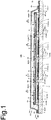
- Fig. 1 is an end view of the cut surface illustrating a photoelectric conversion element according to a preferred embodiment of the invention.
- Fig. 2 is a plan view illustrating a portion of the photoelectric conversion element according to the preferred embodiment of the invention.
- Fig. 3 is a plan view illustrating a pattern of transparent conductive layers in the photoelectric conversion element of Fig. 1 .
- Fig. 4 is a partial plan view illustrating a bottom of a groove between adjacent transparent conductive layers in Fig. 3 .
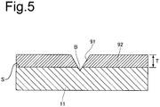
- Fig. 5 is a partial end view of the cut surface taken along line V-V in Fig. 4 .
- Fig. 1 is an end view of the cut surface illustrating a photoelectric conversion element according to a preferred embodiment of the invention.
- Fig. 2 is a plan view illustrating a portion of the photoelectric conversion element according to the preferred embodiment of the invention.
- Fig. 3 is a plan view illustrating a pattern of transparent conductive layers in the photoelectric conversion element of Fig. 1
- FIG. 6 is a plan view illustrating a first integrated sealing portion in Fig. 1 .
- Fig. 7 is a plan view illustrating a second integrated sealing portion in Fig. 1 .
- Fig. 8 is a partial end view of the cut surface taken along line VIII-VIII in Fig. 2 .
- Fig. 9 is a plan view illustrating a conductive substrate where an insulating material, a connecting portion for fixing a back sheet, and an oxide semiconductor layer are formed.
- the photoelectric conversion element 100 includes a conductive substrate 15 provided with a transparent substrate 11 and a plurality of transparent conductive layers 12 which are arranged on the transparent substrate 11 with grooves 90 interposed therebetween.
- the photoelectric conversion element 100 includes one transparent substrate 11 and a plurality (four in the embodiment) of photoelectric conversion cells 50 formed on the transparent substrate 11.
- the plurality of photoelectric conversion cells 50 will be referred to as photoelectric conversion cells 50A to 50D as necessary.
- the photoelectric conversion cell 50 includes one transparent conductive layer 12 of the plurality of transparent conductive layers 12, a counter substrate 20 facing the transparent conductive layer 12, and an oxide semiconductor layer 13 provided between the transparent conductive layer 12 and the counter substrate 20.
- the oxide semiconductor layer 13 is provided on the transparent conductive layer 12.
- the conductive substrate 15 and the counter substrate 20 are joined by an annular sealing portion 30A, and the cell space formed by the conductive substrate 15, the counter substrate 20, and the annular sealing portion 30A is filled with the electrolyte 40.
- the oxide semiconductor layer 13 is arranged inside the annular sealing portion 30A, and the oxide semiconductor layer 13 carries a dye.
- the plurality of photoelectric conversion cells 50 are connected in series by conductive materials 60P.
- a back sheet 80 is provided on the side of the photoelectric conversion cell 50 facing the counter substrate 20 (refer to Fig. 1 ).
- the counter substrate 20 is constituted by a counter electrode and includes a metal substrate 21 as an electrode and a catalyst layer 22 provided on the side of the metal substrate 21 facing the conductive substrate 15 to facilitate a catalytic reaction.
- the counter substrates 20 are separated from each other.
- the conductive substrate 15 has a transparent substrate 11 and a plurality of transparent conductive layers 12A to 12F as electrodes which are arranged on the transparent substrate 11 with the grooves 90 interposed therebetween.
- the transparent conductive layers 12A to 12F are transparent conductive layers 12 constituting the electrodes of the photoelectric conversion cells 50A to 50D.
- the transparent conductive layers 12E and 12F are the transparent conductive layers 12 which do not constitute the electrodes of the photoelectric conversion cells 50A to 50D.
- the transparent conductive layers 12E and 12F are provided around the transparent conductive layers 12A to 12D.
- the transparent conductive layer 12E is arranged so as to be bent along the sealing portion 30A.
- the transparent conductive layer 12F is an annular transparent conductive layer 12 for fixing the peripheral portion 80a of the back sheet 80 (refer to Fig. 1 ) .
- all of the transparent conductive layers 12A to 12D have a quadrangular-shaped main body portion 12a having a side edge portion 12b and a protruding portion 12c which laterally protrudes from the side edge portion 12b of the main body portion 12a.
- the protruding portion 12c of the transparent conductive layer 12C of the photoelectric conversion cell 50C among the transparent conductive layers 12A to 12D has a projecting portion 12d which laterally projects with respect to the arrangement direction X of the photoelectric conversion cells 50A to 50D and a facing portion 12e which extends from the projecting portion 12d and faces the main body portion 12a of the adjacent photoelectric conversion cell 50D via the groove 90.
- the protruding portion 12c of the transparent conductive layer 12B has the projecting portion 12d and the facing portion 12e.
- the protruding portion 12c of the transparent conductive layer 12A has the projecting portion 12d and the facing portion 12e.
- the photoelectric conversion cell 50D is connected with the photoelectric conversion cell 50C already and there is no other photoelectric conversion cell 50 to be connected. For this reason, in the photoelectric conversion cell 50D, the protruding portion 12c of the transparent conductive layer 12D does not have a facing portion 12e. In other words, the protruding portion 12c of the transparent conductive layer 12D is constituted by only the projecting portion 12d.
- the transparent conductive layer 12D further has a first current extracting portion 12f for extracting the current generated in the photoelectric conversion element 100 to the outside and a connecting portion 12g which connects the first current extracting portion 12f and the main body portion 12a and extends along the side edge portion 12b of the transparent conductive layers 12A to 12C.
- the first current extracting portion 12f is disposed in the vicinity of the photoelectric conversion cell 50A and on the side opposite to the transparent conductive layer 12B with respect to the transparent conductive layer 12A.
- the transparent conductive layer 12E also includes a second current extracting portion 12h for extracting the current generated by the photoelectric conversion element 100 to the outside, and the second current extracting portion 12h is arranged in the vicinity of the photoelectric conversion cell 50A and on the side opposite to the transparent conductive layer 12B with respect to the transparent conductive layer 12A.
- the first current extracting portion 12f and the second current extracting portion 12h are arranged to be adjacent to each other via the groove 90B (90) in the periphery of the photoelectric conversion cell 50A.
- the groove 90 is configured by a first groove 90A which is formed along an edge portion of the main body portion 12a of the transparent conductive layer 12 and a second groove 90B which is formed along an edge portion of a portion of the transparent conductive layer 12 excluding the main body portion 12a and intersects the peripheral edge portion 80a of the back sheet 80.
- the cracks 91 extend from each of the edges on both sides of the groove 90 toward the edge on the opposite side of the groove 90.
- the cracks 91 are in contact with the edge of the groove 90, that is, the transparent conductive layer 12.
- the cracks 91 having a length of 5 ⁇ m or more exist in the conductive film 92 at a ratio of 15 or more per 100 ⁇ m in length along the longitudinal direction of the groove 90.
- the connecting terminals 16 are provided on each of the protruding portions 12c of the transparent conductive layers 12A to 12C and the transparent conductive layer 12E.
- Each connecting terminal 16 has a conductive material connecting portion 16A which is connected to the conductive material 60P and extends along the sealing portion 30A outside the sealing portion 30A and a conductive material non-connecting portion 16B which extends from the conductive material connecting portion 16A along the sealing portion 30A outside the sealing portion 30A.
- the conductive material connecting portion 16A of the connecting terminal 16 is provided on the counter portion 12e of the protruding portion 12c and faces the main body portion 12a of the connected adjacent photoelectric conversion cell 50.
- the conductive material connecting portion 16A of the connecting terminal 16 faces the main body portion 12a of the connected adjacent photoelectric conversion cell 50A.
- the conductive material connecting portion 16A of the connecting terminal 16 provided on the protruding portion 12c of the transparent conductive layer 12C in the photoelectric conversion cell 50C is connected to the metal substrate 21 of the counter substrate 20 in the adjacent photoelectric conversion cell 50D through the conductive material 60P.
- the conductive material 60P is arranged so as to pass on the sealing portion 30A.
- the conductive material connecting portion 16A of the connecting terminal 16 in the photoelectric conversion cell 50B is connected to the metal substrate 21 of the counter substrate 20 in the adjacent photoelectric conversion cell 50C through the conductive material 60P
- the conductive material connecting portion 16A of the connecting terminal 16 in the photoelectric conversion cell 50A is connected to the metal substrate 21 of the counter substrate 20 in the adjacent photoelectric conversion cell 50B through the conductive material 60P
- the conductive material connecting portion 16A of the connecting terminal 16 on the transparent conductive layer 12E is connected to the metal substrate 21 of the counter substrate 20 in the adjacent photoelectric conversion cell 50A through the conductive material 60P.
- external connecting terminals 18a and 18b are provided on first and second current extracting portions 12f and 12h, respectively.
- the sealing portion 30A includes an annular first sealing portion 31A which is provided between the conductive substrate 15 and the counter substrate 20 and a second sealing portion 32A provided so as to overlap with the first sealing portion 31A and which interposes an edge portion 20a of the counter substrate 20, together with the first sealing portion 31A.
- the first sealing portions 31A adjacent to each other are integrated to constitute a first integrated sealing portion 31.
- the first integrated sealing portion 31 is constituted by an annular portion (hereinafter, referred to as an "annular portion”) 31a which is not provided between the two counter substrates 20 adjacent to each other and a portion (hereinafter, referred to as a "partitioning portion”) 31b which is provided between the two counter substrates 20 adjacent to each other and partitions an inner opening 31c of the annular portion 31a.
- the second sealing portions 32A are integrated between the counter substrates 20 adjacent to each other to constitute a second integrated sealing portion 32.
- the second integrated sealing portion 32 is constituted by an annular portion (hereinafter, referred to as a "annular portion”) 32a which is not provided between the two counter substrates 20 adjacent to each other and a portion (hereinafter, referred to as a "partitioning portion”) 32b which is provided between the two counter substrates 20 adjacent to each other and partitions an inner opening 32c of the annular portion 32a.
- an insulating material 33 is provided so as to enter the groove 90 between the adjacent transparent conductive layers 12A to 12F and extend over the adjacent transparent conductive layers 12. Namely, the portion of the groove 90 along the first sealing portion 31A is covered with the insulating material 33.
- the second integrated sealing portion 32 includes a main body portion 32d provided on the side of the counter substrate 20 opposite to the conductive substrate 15 and an adhesive portion 32e provided between the adjacent counter substrates 20.
- the second integrated sealing portion 32 is adhered to the first integrated sealing portion 31 by the adhesive portion 32e.
- a back sheet 80 is provided on the conductive substrate 15.
- the back sheet 80 includes a stacked body 80A including a weather resistant layer and a metal layer and an adhesive portion 80B provided in the side opposite to the metal layer with respect to the stacked body 80A and adhered to the conductive substrate 15 via a coupling portion 14.
- the adhesive portion 80B is used to adhere the back sheet 80 to the conductive substrate 15, and as illustrated in Fig. 1 , the adhesive portion may be formed in the peripheral edge portion of the stacked body 80A. However, the adhesive portion 80B may be provided over the entire surface of the side of the stacked body 80A facing the photoelectric conversion cell 50 of the stacked body 80A.
- the peripheral edge portion 80a of the back sheet 80 is connected to the transparent conductive layers 12D, 12E, and 12F of the transparent conductive layers 12 via the coupling portion 14 by the adhesive portion 80B.
- the adhesive portion 80B is separated from the sealing portion 30A of the photoelectric conversion cell 50.
- the coupling portion 14 is also separated from the sealing portion 30A.
- a current collecting wiring 17 having a lower resistance than that of the transparent conductive layer 12D extends so as to pass through the main body portion 12a, the connecting portion 12g, and the current extracting portion 12f.
- This current collecting wiring 17 is disposed so as not to intersect with the coupling portion 14 of the back sheet 80 and the conductive substrate 15. In other words, the current collecting wiring 17 is disposed on the inner side than the coupling portion 14.
- bypass diodes 70A to 70D are connected in parallel with the photoelectric conversion cells 50A to 50D, respectively.
- the bypass diode 70A is fixed on the partitioning portion 32b of the second integrated sealing portion 32 between the photoelectric conversion cell 50A and the photoelectric conversion cell 50B
- the bypass diode 70B is fixed on the partitioning portion 32b of the second integrated sealing portion 32 between the photoelectric conversion cell 50B and the photoelectric conversion cell 50C
- the bypass diode 70C is fixed on the partitioning portion 32b of the second integrated sealing portion 32 between the photoelectric conversion cell 50C and the photoelectric conversion cell 50D.
- the bypass diode 70D is fixed on the sealing portion 30A of the photoelectric conversion cell 50D.
- the conductive material 60Q is fixed to the metal substrate 21 of the counter substrate 20 so as to pass through the bypass diodes 70A to 70D.
- the conductive material 60P branches out from the conductive materials 60Q between the bypass diodes 70A and 70B, between the bypass diodes 70B and 70C, and between the bypass diodes 70C and 70D, respectively, and is connected with the conductive material connecting portion 16A on the transparent conductive layer 12A, the conductive material connecting portion 16A on the transparent conductive layer 12B, and the conductive material connecting portion 16A on the transparent conductive layer 12C, respectively.
- the conductive material 60P is also fixed to the metal substrate 21 of the counter substrate 20 of the photoelectric conversion cell 50A, and this conductive material 60P connects the bypass diode 70A and the conductive material connecting portion 16A of the connecting terminal 16 on the transparent conductive layer 12E. Moreover, the bypass diode 70D is connected with the transparent conductive layer 12D via the conductive material 60P.
- a desiccant 95 is provided on the counter substrate 20 of each photoelectric conversion cell 50.
- the cracks 91 having a length of 5 ⁇ m or more exist at a ratio of 15 or more per 100 ⁇ m in length along the longitudinal direction of the groove 90. For this reason, since the conductive path in the conductive film 92 is sufficiently cut by the cracks 91, the insulation between the transparent conductive layers 12 can be sufficiently secured. As a result, it is possible to improve the photoelectric conversion characteristics of the photoelectric conversion element 100.
- the cracks 91 are in contact with the edge of the groove 90, that is, the transparent conductive layer 12. Therefore, as compared with a case where the cracks 91 are not in contact with the edge of the groove 90, that is, the transparent conductive layer 12, the insulation between the adjacent transparent conductive layers 12 is further improved.
- the portion of the groove 90 along the first sealing portion 31A is covered with the insulating material 33.
- the insulating material enters the cracks 91 existing in the groove 90, the insulation between the transparent conductive layers 12 can be more sufficiently secured.
- the sealing portion 30A and the insulating material 33 are arranged so as to overlap with each other. For this reason, as compared with a case where the insulating material 33 is arranged so as not to overlap with the sealing portion 30A, it is possible to further increase the area of the portion contributing to power generation as viewed from the light receiving surface side of the photoelectric conversion element 100. Therefore, it is possible to further improve the aperture ratio.
- the first current extracting portion 12f and the second current extracting portion 12h are disposed in the vicinity of the photoelectric conversion cell 50A and on the side opposite to the transparent conductive layer 12B with respect to the transparent conductive layer 12A, and the first current extracting portion 12f of the transparent conductive layer 12A and the second current extracting portion 12h of the transparent conductive layer 12F are disposed so as to be adjacent to each other via the groove 90.
- the photoelectric conversion element 100 it is possible to dispose the external connecting terminals 18a and 18b to the first current extracting portion 12f and the second current extracting portion 12h, respectively, so as to be adjacent to each other.
- the number of connectors for extracting the current from the external connecting terminals 18a and 18b is set to one.
- the external connecting terminals 18a and 18b are also disposed to be greatly spaced apart from each other since the first current extracting portion 12f and the second current extracting portion 12h are disposed to be greatly spaced apart from each other.
- two connectors of a connector to be connected with the external connecting terminal 18a and a connector to be connected with the external connecting terminal 18b are required in order to extract the current from the photoelectric conversion element 100.
- the generated current is low in the photoelectric conversion element 100 when the photoelectric conversion element 100 is used under a low illuminance. Specifically, the generated current is 2 mA or lower.
- the photoelectric conversion cells 50A to 50D are arranged in a line along the X direction, the transparent conductive layer 12D of the photoelectric conversion cell 50D on one end side of the photoelectric conversion cell 50A and photoelectric conversion cell 50D at both ends of the photoelectric conversion cells 50A to 50D has the main body portion 12a provided on the inner side of the sealing portion 30A, the first current extracting portion 12f, and the connecting portion 12g which connects the main body portion 12a and the first current extracting portion 12f. For this reason, it is possible to more shorten the installation region of the connecting terminal 16 provided along the arrangement direction (X direction in Fig.
- the photoelectric conversion element 100 since the generated current is usually low in a case in which the photoelectric conversion element 100 is used in a low illuminance environment, it is possible to sufficiently suppress the deterioration of the photoelectric conversion characteristics even if the photoelectric conversion element 100 further has the first connecting portion 12g which connects the main body portion 12a and the first current extracting portion 12f.
- the current collecting wiring 17 is arranged so as not to intersect the coupling portion 14 between the back sheet 80 and the conductive substrate 15. Since the current collecting wiring 17 is generally porous, the current collecting wiring has gas permeability, and thus, gases such as water vapor are permeable. However, the current collecting wiring 17 is arranged so as not to intersect the coupling portion 14 between the back sheet 80 and the conductive substrate 15. For this reason, the infiltration of water vapor or the like from the outside through the current collecting wiring 17 into the space between the back sheet 80 and the conductive substrate 15 can be prevented. As a result, the photoelectric conversion element 100 can have excellent durability. In addition, since the current collecting wiring 17 has a resistance lower than that of the transparent conductive layer 12D, even when the generated current becomes large, a deterioration in photoelectric conversion characteristics can be sufficiently suppressed.
- the conductive material 60P connected with the metal substrate 21 of the counter substrate 20 of one photoelectric conversion cell 50 of two adjacent photoelectric conversion cells 50 is connected with the conductive material connecting portion 16A on the protruding portion 12c of the other photoelectric conversion cell 50, and the conductive material connecting portion 16A is provided on the protruding portion 12c and on the outer side of the sealing portion 30A.
- the connection of two adjacent photoelectric conversion cells 50 is performed on the outer side of the sealing portion 30A. For this reason, according to the photoelectric conversion element 100, it is possible to improve the aperture ratio.
- the protruding portion 12c in the photoelectric conversion cell 50 that is connected with the adjacent photoelectric conversion cell 50 among the photoelectric conversion cells 50A to 50D, has the projecting portion 12d which laterally projects from the main body portion 12a and the facing portion 12e which extends from the projecting portion 12d and faces the main body portion 12a of the adjacent photoelectric conversion cell 50, and at least the conductive material connecting portion 16A of the connecting terminal 16 is provided on the facing portion 12e.
- the conductive material connecting portion 16A of the connecting terminal 16 is provided on the facing portion 12e facing the main body portion 12a of the adjacent photoelectric conversion cell 50, it is possible to sufficiently prevent the conductive material 60P connected with the conductive material connecting portion 16A from passing over the metal substrate 21 of the counter substrate 20 of the adjacent photoelectric conversion cell 50 unlike the case in which at least the conductive material connecting portion 16A of the connecting terminal 16 is not provided on the facing portion 12e facing the main body portion 12a of the adjacent photoelectric conversion cell 50. As a result, it is possible to sufficiently prevent the short circuit between the adjacent photoelectric conversion cells 50.
- both of the conductive material connecting portion 16A and the conductive material non-connecting portion 16B are disposed along the sealing portion 30A. For this reason, it is possible to save the space required for the connecting terminal 16 compared to the case of disposing the conductive material connecting portion 16A and the conductive material non-connecting portion 16B along the direction away from the sealing portion 30A.
- the adhesive portion 80B of the back sheet 80 is spaced apart from the sealing portion 30A of the photoelectric conversion cell 50. For this reason, it is sufficiently suppressed that the sealing portion 30A is stretched since the adhesive portion 80B is constricted at a low temperature and thus an excessive stress is applied to the interface between the sealing portion 30A and the conductive substrate 15 or the counter substrate 20. In addition, at a high temperature as well, it is sufficiently suppressed that the sealing portion 30A is pressed since the adhesive portion 80B expands and thus an excessive stress is applied to the interface between the sealing portion 30A and the conductive substrate 15 or the counter substrate 20.
- the photoelectric conversion element 100 it is sufficiently suppressed that an excessive stress is applied to the interface between the sealing portion 30A and the conductive substrate 15 or the counter substrate 20 both at a high temperature and a low temperature. For this reason, it is possible for the photoelectric conversion element 100 to have excellent durability.
- the second sealing portion 32A is adhered to the first sealing portion 31A, and the edge portion 20a of the counter substrate 20 is sandwiched by the first sealing portion 31A and the second sealing portion 32A. For this reason, even when stress is applied to the counter substrate 20 in a direction in which the counter substrate is separated from the conductive substrate 15, its peeling-off is sufficiently suppressed by the second sealing portion 32A. Further, since the partitioning portion 32b of the second integrated sealing portion 32 is adhered to the first sealing portion 31A through the gap S between the adjacent counter substrates 20. For this reason, the counter substrates 20 of the photoelectric conversion cells 50 adjacent to each other are reliably prevented from contacting each other.
- the conductive substrate 15, the oxide semiconductor layer 13, the insulating material 33, the coupling portion 14, the dye, the counter substrate 20, the sealing portion 30A, the electrolyte 40, the conductive materials 60P and 60Q, the back sheet 80, and the desiccant 95 will be described in detail.
- the conductive substrate 15 has the transparent substrate 11 and the plurality of transparent conductive layers 12A to 12F.
- the material constituting the transparent substrate 11 may be any transparent material, for example, and examples of such a transparent material include glass such as borosilicate glass, soda lime glass, glass which is made of soda lime and whose iron component is less than that of ordinary soda lime glass, and quartz glass, polyethylene terephthalate (PET), polyethylene naphthalate (PEN), polycarbonate (PC), and polyethersulfone (PES).
- the thickness of the transparent substrate 11 is appropriately determined depending on the size of the photoelectric conversion element 100 and is not particularly limited, but it may be set into the range of from 50 to 10000 ⁇ m, for example.
- the material contained in the transparent conductive layer 12 examples include a conductive metal oxide such as indium-tin-oxide (ITO), tin oxide (Sn0 2 ), and fluorine-doped-tin-oxide (FTO).
- the transparent conductive layer 12 may be constituted by a single layer or a laminate consisting of a plurality of layers containing different conductive metal oxides. It is preferable that the transparent conductive layer 12 contain FTO since FTO exhibits high heat resistance and chemical resistance in a case in which the transparent conductive layer 12 is constituted by a single layer.
- the transparent conductive layer 12 may further contain a glass frit.
- the thickness of the transparent conductive layer 12 may be set into the range of from 0.01 to 2 ⁇ m, for example.
- the width W of the groove 90 is not particularly limited, but the width of the groove is preferably 400 ⁇ m or less (refer to Fig. 4 ). In this case, it is possible to save extra space as compared with a case where the width W of the groove 90 is more than 400 ⁇ m.
- the width W of the groove 90 is preferably 250 ⁇ m or less, more preferably 220 ⁇ m or less, and still more preferably 200 ⁇ m or less.
- the width W of the groove 90 is preferably 40 ⁇ m or more. In this case, as compared with a case where the width W of the groove 90 is less than 40 ⁇ m, it is possible to further improve the insulation between the adjacent transparent conductive layers 12.
- the width W of the groove 90 is more preferably 60 ⁇ m or more, and more preferably 80 ⁇ m or more.
- the conductive film 92 is made of the same material as the transparent conductive layer 12.
- the maximum thickness of the conductive film 92 is not particularly limited, but the maximum thickness is preferably 150 nm or less. In this case, as compared with a case where the maximum thickness of the conductive film 92 is more than 150 nm, the resistance between the two adjacent transparent conductive layers 12 is reduced, so that it is possible to further improve the photoelectric conversion characteristics of the photoelectric conversion element 100.
- the maximum thickness of the conductive film 92 is preferably 100 nm or less, and more preferably 70 nm or less. However, the maximum thickness of the conductive film 92 is preferably 30 nm or more, and more preferably 50 nm or more.
- the cracks 91 having a length of 5 ⁇ m or more along the longitudinal direction of the groove 90 between the plurality of transparent conductive layers 12 may exist in the conductive film 92 provided on the transparent substrate 11 at a ratio of 15 or more per 100 ⁇ m in length along the longitudinal direction of the groove 90, it is preferable that the cracks 91 having a length of 5 ⁇ m or more exist in the conductive film 92 at a ratio of 20 or more per 100 ⁇ m in length along the longitudinal direction of the groove 90. In this case, it is possible to further improve the photoelectric conversion characteristics of the photoelectric conversion element 100.
- the cracks 91 having a length of 5 ⁇ m or more exist in the conductive film 92 at a ratio of 34 or more per 100 ⁇ m in length along the longitudinal direction of the groove 90. In this case, it is possible to further improve the photoelectric conversion characteristics of the photoelectric conversion element.
- the cracks 91 exist in the conductive film 92 at a ratio of 200 or less per 100 ⁇ m in length along the longitudinal direction of the groove 90.
- the transparency of the groove 90 becomes high as compared with a case where the cracks 91 exist in the conductive film 92 at a ratio of more than 200 per 100 ⁇ m in length along the longitudinal direction of the groove 90.
- the cracks 91 exist more preferably at a ratio of 100 or less per 100 ⁇ m in length along the longitudinal direction of the groove 90, still more preferably at a ratio of 50 or less per 100 ⁇ m in length along the longitudinal direction of the groove 90, and particularly preferably at a ratio of 40 or less per 100 ⁇ m in length along the longitudinal direction of the groove 90.
- the bottom B of the cracks 91 may or may not reach the interface S between the transparent substrate 11 and the conductive film 92, but the bottom B of the cracks preferably reaches the interface S. In this case, since the conductive path is cut in the length direction of the cracks 91, the resistance of the conductive film 92 can be further increased.
- the maximum thickness of the conductive film 92 be 150 nm or less, and the width W of the groove 90 be 200 nm or less.
- the maximum thickness of the conductive film 92 is preferably 100 nm or less, and more preferably 70 nm or less. However, the maximum thickness of the conductive film 92 is preferably 30 nm or more, and more preferably 50 nm or more.
- the width W of the groove 90 is preferably 40 ⁇ m or more. In this case, as compared with a case where the width W of the groove 90 is less than 40 ⁇ m, the insulation between the adjacent transparent conductive layers 12 is further improved.
- the width W of the groove 90 is more preferably 60 ⁇ m or more, and still more preferably 80 ⁇ m or more.
- the bottom B of the cracks 91 reach a position farther from the conductive film 92 than the interface S in the transparent substrate 11. In this case, since the conductive path is cut more reliably in the length direction of the cracks 91, the resistance of the conductive film 92 can be further increased.
- the connecting terminal 16 contains a metallic material.
- the metallic material include silver, copper and indium. These may be used singly or in combination of two or more kinds thereof.
- the connecting terminal 16 may be constituted by the same material as or a different material from the conductive material 60P but it is preferable to be constituted by the same material.
- the oxide semiconductor layer 13 is constituted by oxide semiconductor particles.
- oxide semiconductor particles is constituted by, for example, titanium oxide (TiO 2 ), silicon oxide (SiO 2 ), zinc oxide (ZnO), tungsten oxide (WO 3 ), niobium oxide (Nb 2 O 5 ), strontium titanate (SrTiO 3 ) or tin oxide (SnO 2 ).
- the insulating material 33 an inorganic insulating material or an organic insulating material may be used. Among them, the inorganic insulating material is preferable as the insulating material 33. In this case, since the inorganic insulating material is hardly deteriorated as compared with the organic insulating material, it is possible to further improve the durability of the photoelectric conversion element 100.
- the inorganic insulating material for example, glass frit or the like may be used.
- thermosetting resin such as a polyimide resin or a thermoplastic resin may be used.
- the material constituting the coupling portion 14 is not particularly limited as long as it can make the back sheet 80 adhere to the transparent conductive layer 12, and it is possible to use, for example, a glass frit, a resin material which is the same as the resin material used for the sealing portion 31A, or the like as the material constituting the coupling portion 14.
- the coupling portion 14 is preferably a glass frit. It is possible to effectively suppress the penetration of moisture or the like from the outside of the back sheet 80 since the glass frit exhibits higher sealing ability than the resin material.
- a photosensitizing dye such as a ruthenium complex having a ligand including a bipyridine structure, a terpyridine structure, or the like, an organic dye such as porphyrin, eosin, rhodamine, or merocyanine; and an organic- inorganic composite dye such as a halogenated lead-based perovskite crystal may be exemplified.
- a photosensitizing dye configured by the ruthenium complex having a ligand including a bipyridine structure or a terpyridine structure is preferred. In this case, it is possible to more improve the photoelectric conversion characteristic of the photoelectric conversion element 100. Meanwhile, in a case where a photosensitizing dye is used as the dye, the photoelectric conversion element 100 becomes a dye-sensitized photoelectric conversion element.
- the counter substrate 20 comprises the metal substrate 21 and a conductive catalyst layer 22 which is provided on the side of the metal substrate 21 facing the conductive substrate 15 and promotes the reduction reaction on the surface of the counter substrate 20.
- the metal substrate 21 is constituted by, for example, a corrosion-resistant metallic material such as titanium, nickel, platinum, molybdenum, tungsten, aluminum, stainless steel or the like.
- the thickness of the metal substrate 21 is appropriately determined depending on the size of the photoelectric conversion element 100 and is not particularly limited, but it may be set to from 0.005 to 0.1 mm, for example.
- the catalytic layer 22 is constituted by platinum, a carbon-based material, a conductive polymer, or the like.
- a carbon nanotube is preferably used as the carbon-based material.
- the sealing portion 30A is constituted by the first sealing portion 31A and the second sealing portion 32A.
- Examples of the material constituting the first sealing portion 31A include a resin such as a modified polyolefin resin including an ionomer, an ethylene-vinyl acetic anhydride copolymer, an ethylene-methacrylic acid copolymer, an ethylene-vinyl alcohol copolymer and the like, an ultraviolet-cured resin, and a vinyl alcohol polymer.
- a resin such as a modified polyolefin resin including an ionomer, an ethylene-vinyl acetic anhydride copolymer, an ethylene-methacrylic acid copolymer, an ethylene-vinyl alcohol copolymer and the like, an ultraviolet-cured resin, and a vinyl alcohol polymer.
- the thickness of the first sealing portion 31A is typically from 20 to 90 ⁇ m and preferably from 40 to 80 ⁇ m.
- the material constituting the second sealing portion 32A examples include a resin such as a modified polyolefin resin including an ionomer, an ethylene-vinyl acetic anhydride copolymer, an ethylene-methacrylic acid copolymer, an ethylene-vinyl alcohol copolymer and the like, an ultraviolet-cured resin, and a vinyl alcohol polymer in the same manner as the first sealing portion 31A.
- the material constituting the second sealing portion 32A may be the same as or different from the material constituting the first sealing portion 31A, but it is preferably the same material. In this case, the infiltration of moisture from the outside and the leakage of the electrolyte 40 can effectively be suppressed since there is no interface between the second sealing portion 32A and the first sealing portion 31A.
- the thickness of the second sealing portion 32A is typically from 20 to 45 ⁇ m and preferably from 30 to 40 ⁇ m.
- the electrolyte 40 contains, a redox couple and an organic solvent, for example. It is possible to use acetonitrile, methoxy acetonitrile, methoxy propionitrile, propionitrile, ethylene carbonate, propylene carbonate, diethyl carbonate, ⁇ -butyrolactone, valeronitrile as the organic solvent.
- the redox couple examples include a redox couple such as a zinc complex, an iron complex, and a cobalt complex in addition to a redox couple containing a halogen atom such as iodide ion/polyiodide ion (for example, I - /I 3 - ), bromine ion/polybromide ion or the like.
- iodine ion/polyiodide ion can be formed by iodine (I 2 ) and a salt (an ionic liquid or a solid salt) containing iodide (I - ) as an anion.
- ionic liquid having iodide as an anion only iodide may be added.
- a salt containing iodide (I - ) as an anion such as LiI, tetrabutylammonium iodide or the like may be added.
- the electrolyte 40 may use an ionic liquid instead of the organic solvent.
- an ionic liquid for example, an ordinary temperature molten salt which is a known iodine salt, such as a pyridinium salt, an imidazolium salt, or a triazolium salt, and which is in a molten state at around room temperature is used.
- an ordinary temperature molten salt for example, 1-hexyl-3-methylimidazolium iodide, 1-ethyl-3-propylimidazolium iodide, 1-ethyl-3-methylimidazolium iodide, 1,2-dimethyl-3-propylimidazolium iodide, 1-butyl-3-methylimidazolium iodide, or 1-methyl-3-propylimidazolium iodide is preferably used.
- the electrolyte 40 may use a mixture of the above ionic liquid and the above organic solvent instead of the above organic solvent.
- an additive to the electrolyte 40.
- the additive include LiI, tetrabutylammonium iodide, 4-t-butylpyridine, guanidium thiocyanate, 1-methylbenzimidazole, and 1-butylbenzimidazole.
- a nanocomposite gel electrolyte which is a quasi-solid electrolyte obtained by kneading nanoparticles such as SiO 2 , TiO 2 , and carbon nanotubes with the above electrolyte to form a gel-like form may be used, or an electrolyte gelled using an organic gelling agent such as polyvinylidene fluoride, a polyethylene oxide derivative, and an amino acid derivative may also be used.
- the electrolyte 40 contains a redox couple including iodide ions/polyiodide ions (for example, I - /I 3 - ), and a concentration of the polyiodide ions (for example, I 3 - ) is preferably 0.010 mol/L or less, more preferably 0.005 mol/L or less, and even more preferably in a range of 0 to 2 ⁇ 10 -4 mol/L.
- concentration of mol/L or less for carrying electrons is low, leakage current can be further reduced. For this reason, an open circuit voltage can be further increased, and thus the photoelectric conversion characteristics can be further improved.
- a metal film is used as the conductive materials 60P and 60Q. It is possible to use, for example, silver or copper as the metallic material constituting the metal film.
- the back sheet 80 includes the stacked body 80A including the weather resistant layer and the metal layer and the adhesive portion 80B which is provided on the surface of the photoelectric conversion cell 50 side of the stacked body 80A and adheres the stacked body 80A and the coupling portion 14.
- the weather resistant layer may be constituted by, for example, polyethylene terephthalate or polybutylene terephthalate.
- the thickness of the weather resistant layer may be from 50 to 300 ⁇ m, for example.
- the metal layer may be constituted by, for example, a metallic material containing aluminum.
- the metallic material is typically constituted by aluminum simple substance but may be an alloy of aluminum and other metals.
- the other metals include, for example, copper, manganese, zinc, magnesium, lead, and bismuth.
- a 1000 series aluminum is desirable in which other metals are added to pure aluminum of 98% or higher purity in a trace quantity. This is because this 1000 series aluminum is inexpensive and excellent in workability compared to other aluminum alloys.
- the thickness of the metal layer is not particularly limited but may be from 12 to 30 ⁇ m, for example.
- the stacked body 80A may further include a resin layer.
- the material constituting the resin layer include a butyl rubber, a nitrile rubber, and a thermoplastic resin. These can be used singly or in combination of two or more kinds thereof.
- the resin layer may be formed on the entire surface on the side opposite to the weather resistant layer of the metal layer or may be formed only on the peripheral portion thereof.
- Examples of the material constituting the adhesive portion 80B include a butyl rubber, a nitrile rubber, and a thermoplastic resin. These can be used singly or in combination of two or more kinds thereof.
- the thickness of the adhesive portion 80B is not particularly limited but may be from 300 to 1000 ⁇ m, for example.
- the desiccant 95 may be in a sheet shape or granular.
- the desiccant 95 may be one which absorbs moisture, for example, and examples of the desiccant 95 include silica gel, alumina, and zeolite.
- Fig. 10 is a plan view illustrating a first integrated sealing portion forming body for forming a first integrated sealing portion of Fig. 6 .
- a laminate obtained by forming a transparent conductive film on one transparent substrate 11 is prepared.
- a sputtering method As the method of forming the transparent conductive film, a sputtering method, a vapor deposition method, a spray pyrolysis deposition method (SPD), or a CVD method is used.
- the groove 90 is formed with respect to the transparent conductive film, and the transparent conductive layers 12A to 12F which are disposed in an insulated state to interpose the groove 90 between one another are formed.
- the four transparent conductive layers 12A to 12D corresponding to the photoelectric conversion cells 50A to 50D are formed so as to have the quadrangular-shaped main body portion 12a and the protruding portion 12c.
- the transparent conductive layers 12A to 12C corresponding to the photoelectric conversion cells 50A to 50C are formed such that the protruding portion 12c has not only the projecting portion 12d but also the facing portion 12e which extends from the projecting portion 12d and faces the main body portion 12a of the adjacent photoelectric conversion cell 50.
- the transparent conductive layer 12D is formed so as to have not only the quadrangular-shaped main body portion 12a and the projecting portion 12d but also the first current extracting portion 12f and the connecting portion 12g connecting the first current extracting portion 12f and the main body portion 12a.
- the first current extracting portion 12f is formed so as to be disposed on the side opposite to the transparent conductive layer 12B with respect to the transparent conductive layer 12A.
- the transparent conductive layer 12E is formed so as to form the second current extracting portion 12h.
- the second current extracting portion 12h is formed so as to be disposed on the side opposite to the transparent conductive layer 12B with respect to the transparent conductive layer 12A and to be disposed next to the first current extracting portion 12f via the groove 90.
- the groove 90 is formed by a laser scribing method using, for example, a fiber laser as a light source.
- the conductive film 92 is provided on the transparent substrate 11, but in order that the cracks 91 having a length of 5 ⁇ m or more exist in the conductive film 92 at a ratio of 15 cracks/100 ⁇ m or more by generating the cracks 91, rapid cooling of the portion of the groove 90 may be performed after forming the groove 90.
- the rapid cooling of the portion of the groove 90 is performed for the following reason. Namely, in a case where the groove 90 is formed by irradiating the transparent conductive film with a laser beam having high energy such as a fiber laser, the irradiated portion of the transparent conductive film has a high temperature and is melted.
- the temperature of the conductive material is gradually decreased to solidify the conductive material, and the conductive film 92 which is a thin conductive residual film is formed.
- the conductive film 92 in the groove 90 is rapidly cooled, the thin conductive film 92 is thermally contracted after the forming of the groove 90, so that the cracks 91 occur in the conductive film 92. Since the conductive path between the transparent conductive layers 12 is sufficiently cut by the cracks 91, the short circuit between the transparent conductive layers 12 is sufficiently suppressed.
- the rapid cooling can be realized by blowing a compressed air into the groove 90, immersing the conductive film 92 in the groove 90 in water, or the like.
- the rapid cooling is preferably performed by blowing the compressed air.
- the pressure of the compressed air may be, for example, in a range of 0.1 to 0.8 MPa.
- the plurality of transparent conductive layers 12A to 12F are formed on the transparent substrate 11 to obtain the conductive substrate 15.
- precursors of the connecting terminal 16 constituted by the conductive material connecting portion 16A and the conductive material non-connecting portion 16B are formed on the protruding portions 12c of the transparent conductive layers 12A to 12C.
- the precursor of the connecting terminal 16 is formed such that the conductive material connecting portion 16A is provided on the facing portion 12e.
- the precursor of the connecting terminal 16 is also formed on the transparent conductive layer 12E.
- the precursor of the connecting terminal 16 can be formed, for example, by coating and drying a silver paste.
- a precursor of the current collecting wiring 17 is formed on the connecting portion 12g of the transparent conductive layer 12D.
- the precursor of the current collecting wiring 17 can be formed, for example, by coating and drying a silver paste.
- precursors of the external connecting terminals 18a and 18b for extracting the current to the outside are respectively formed on the first current extracting portion 12f of the transparent conductive layer 12A and the second current extracting portion 12h.
- the precursor of the external connecting terminal can be formed, for example, by coating and drying a silver paste.
- a precursor of the insulating material 33 is formed so as to enter into the first groove 90A formed along the edge portion of the main body portion 12a.
- the insulating material 33 can be formed, for example, by coating and drying a paste containing an insulating material such as a glass frit.
- a precursor of the annular coupling portion 14 is formed so as to surround the insulating material 33 and to pass through the transparent conductive layer 12D, the transparent conductive layer 12E, and the transparent conductive layer 12F.
- a precursor of the oxide semiconductor layer 13 is formed on the main body portion 12a of each of the transparent conductive layers 12A to 12D.
- the precursor of the oxide semiconductor layer 13 can be obtained by printing and then drying a paste for oxide semiconductor layer formation for forming the oxide semiconductor layer 13.
- the paste for oxide semiconductor layer formation contains a resin such as polyethylene glycol,ethyl cellulose or the like and a solvent such as terpineol in addition to the oxide semiconductor particles composed of titanium oxide or the like.
- the precursor of the connecting terminal 16, the precursor of the insulating material 33, the precursor of the coupling portion 14, and the precursor of the oxide semiconductor layer 13 are collectively fired to form the connecting terminal 16, the insulating material 33, the coupling portion 14, and the oxide semiconductor layer 13.
- the firing temperature varies depending on the kind of the oxide semiconductor particles or the insulating material 33 but is typically from 350 to 600°C, and the firing time also varies depending on the kind of the oxide semiconductor particles or the insulating material 33 but is typically from 1 to 5 hours.
- the conductive substrate 15 is obtained on which the insulating material 33 and the coupling portion 14 for fixing the back sheet 80 are formed.
- the dye is supported on the oxide semiconductor layer 13.
- the dye may be adsorbed on the oxide semiconductor layer 13 by immersing the oxide semiconductor layer 13 in a solution containing the dye, then washing out the extra dye with the solvent component of the above solution after making the dye adsorb on the oxide semiconductor layer 13, and performing drying.
- the electrolyte 40 is disposed on the oxide semiconductor layer 13.
- a first integrated sealing portion forming body 131 for forming the first integrated sealing portion 31 is prepared.
- the first integrated sealing portion forming body 131 can be obtained by preparing one sheet of resin film for sealing composed of the material constituting the first integrated sealing portion 31 and forming a quadrangular-shaped opening 131a in the resin film for sealing as many as the number of the photoelectric conversion cells 50.
- the first integrated sealing portion forming body 131 has a structure obtained by integrating a plurality of first sealing portion forming bodies 131A.
- this first integrated sealing portion forming body 131 is adhered on the conductive substrate 15. At this time, the first integrated sealing portion forming body 131 is adhered so as to be superimposed on the insulating material 33.
- the adhesion of the first integrated sealing portion forming body 131 to the conductive substrate 15 can be performed by heating and melting the first integrated sealing portion forming body 131.
- the first integrated sealing portion forming body 131 is adhered to the conductive substrate 15 such that the main body portion 12a of the transparent conductive layer 12 is disposed on the inner side of the first integrated sealing portion forming body 131A.
- the counter substrates 20 are prepared to have the same number as the number of the photoelectric conversion cells 50.
- the counter substrate 20 can be obtained by forming the conductive catalyst layer 22 which promotes the reduction reaction on the surface of the counter substrate 20 on the metal substrate 21.
- each of the plurality of the counter substrates 20 is bonded so as to close each of the openings 131a of the first integrated sealing portion forming body 131.
- the first integrated sealing portion forming body 131 adhered to the counter substrate 20 and the first integrated sealing portion forming body 131 adhered to the conductive substrate 15 are superposed, and heated and melted while the first integrated sealing portion forming bodies 131 are pressed.
- the first integrated sealing portion 31 is formed between the conductive substrate 15 and the counter substrate 20.
- the first integrated sealing portion 31 may be formed under the atmospheric pressure or under reduced pressure. However, the first integrated sealing portion 31 is preferably formed under reduced pressure.
- the second integrated sealing portion 32 has a structure obtained by integrating a plurality of the first sealing portions 32A.
- the second integrated sealing portion 32 can be obtained by preparing one sheet of resin film for sealing and forming a quadrangular-shaped opening 32c in the resin film for sealing as many as the number of the photoelectric conversion cells 50.
- the second integrated sealing portion 32 is bonded to the counter substrate 20 so as to sandwich the edge portion 20a of the counter substrate 20 together with the first integrated sealing portion 31.
- the adhesion of the second integrated sealing portion 32 to the counter substrate 20 can be performed by heating and melting the second integrated sealing portion 32.
- the resin film for sealing examples include a resin such as a modified polyolefin resin including ionomer, an ethylene-vinyl acetate anhydride copolymer, an ethylene methacrylic acid copolymer, an ethylene-vinyl alcohol copolymer, and the like, an ultraviolet-cured resin, and a vinyl alcohol polymer.
- a constituent material of the resin film for sealing for forming the second integrated sealing portion 32 preferably has a higher melting point than that of the constituent material of the resin film for sealing for forming the first integrated sealing portion 31.
- the second sealing portion 32A is harder than the first sealing portion 31A, it is possible to effectively prevent contact between the counter substrates 20 of the photoelectric conversion cells 50 adjacent to each other.
- the first sealing portion 31A is softer than the second sealing portion 32A, stress applied to the sealing portion 30A can be effectively relieved.
- bypass diodes 70A, 70B, and 70C are fixed to the partitioning portion 32b of the second sealing portion 32.
- the bypass diode 70D is fixed on the sealing portion 30A of the photoelectric conversion cell 50D as well.
- the conductive material 60Q is fixed to the metal substrate 21 of the counter substrate 20 of the photoelectric conversion cells 50B to 50D so as to pass through the bypass diodes 70A to 70D.
- the conductive material 60P is formed such that each of the conductive materials 60Q between the bypass diodes 70A and 70B, between the bypass diodes 70B and 70C, and between the bypass diodes 70C and 70D is connected with the conductive material connecting portion 16A on the transparent conductive layer 12A, the conductive material connecting portion 16A on the transparent conductive layer 12B, and the conductive material connecting portion 16A on the transparent conductive layer 12C, respectively.
- the conductive material 60P is fixed to the metal substrate 21 of the counter substrate 20 of the photoelectric conversion cell 50A so as to connect the conductive material connecting portion 16A on the transparent conductive layer 12E and the bypass diode 70A.
- the transparent conductive layer 12D is connected with the bypass diode 70A by the conductive material 60P.
- a paste containing a metallic material constituting the conductive material 60P is prepared, and this paste is coated from the counter substrate 20 over the conductive material connecting portion 16A of the connecting terminal 16 of the adjacent photoelectric conversion cell 50 and cured.
- a paste containing a metallic material constituting the conductive material 60Q is prepared, and this paste is coated on each of the counter substrates 20 so as to link the adjacent bypass diodes and cured.
- the back sheet 80 is prepared, and the peripheral portion 80a of the back sheet 80 is adhered to the coupling portion 14. At this time, the back sheet 80 is disposed such that the adhesive portion 80B of the back sheet 80 is spaced apart from the sealing portion 30A of the photoelectric conversion cell 50.
- the photoelectric conversion element 100 is obtained in the manner described above.
- a method to collectively fire the precursor of the connecting terminal 16, the precursor of the insulating material 33, the precursor of the coupling portion 14, and the precursor of the oxide semiconductor layer 13 is used in order to form the connecting terminal 16, the insulating material 33, the coupling portion 14, and the oxide semiconductor layer 13, but the connecting terminal 16, the insulating material 33, the coupling portion 14, and the oxide semiconductor layer 13 may be formed by separately firing each of the precursors.
- the invention is not limited to the above-described embodiment.
- the cracks 91 are in contact with the edge portion of the groove 90, that is, the transparent conductive layer 12.
- the cracks are not necessarily in contact with the edge portion of the groove 90.
- the cracks 91a and 91b that intersect with the other cracks 91 exist, but the cracks 91a and 91b that intersect with the other cracks 91 may not exist.
- the cracks 91 may be configured with only the cracks 91c and 91d that do not intersect with the other cracks 91.
- the conductive substrate 15 has the insulating material 33.
- the conductive substrate 15 may not have the insulating material 33.
- the sealing portion 30A and the first integrated sealing portion 31A are directly bonded to the transparent substrate 11 and the transparent conductive layer 12.
- the groove 90 has the second groove 90B, but the second groove 90B may not be necessarily formed.
- the conductive material connecting portion 16A and the conductive material non-connecting portion 16B are provided along the sealing portion 30A, respectively, but these may be formed so as to extend in the direction away from the sealing portion 30A.
- the conductive material connecting portion 16A it is preferable that the conductive material connecting portion 16A be disposed at the position closer to the sealing portion 30A than the conductive material non-connecting portion 16B. In this case, it is possible to more shorten the conductive material 60P.
- the connecting terminal 16 may not be necessarily provided on the transparent conductive layer 12.
- the second sealing portion 32A is adhered to the first sealing portion 31A, but the second sealing portion 32A may not be adhered to the first sealing portion 31A.
- the sealing portion 30A is constituted by the first sealing portion 31A and the second sealing portion 32A, but the second sealing portion 32A may be omitted.
- the back sheet 80 is adhered to the transparent conductive layer 12 via the coupling portion 14, but the back sheet 80 is not necessarily required to be adhered to the transparent conductive layer 12 via the coupling portion 14.
- the coupling portion 14 and the insulating material 33 are separated from each other, but the coupling portion 14 and the insulating material 33 may be integrated.
- the photoelectric conversion element has the back seat 80 in the above embodiment, the photoelectric conversion element may not have the back seat 80.
- the photoelectric conversion element 100 has the bypass diodes in the above-described embodiment, the photoelectric conversion element 100 may not necessarily have the bypass diodes.
- the transparent conductive layer 12 is used as the conductive layer.
- the conductive layer is not necessarily transparent.
- the substrate supporting the conductive layer is not necessarily transparent.
- the oxide semiconductor layer 13 is provided on the transparent conductive layer 12.
- the counter substrate 20 is transparent and conductive, the oxide semiconductor layer 13 may be provided on the counter substrate 20.
- the photoelectric conversion element 100 has the plurality of photoelectric conversion cells 50.
- the transparent conductive layer 12 is arranged on the transparent conductive layer 12 of one photoelectric conversion cell 50 through the groove 90, the photoelectric conversion element may have only one photoelectric conversion cell 50.
- the counter substrate 20 is constituted by the counter electrode, but like the photoelectric conversion element 200 illustrated in Fig. 11 , an insulating substrate 201 may be used instead of the counter electrode as a counter substrate 20.
- a structure 202 is disposed in a space between an insulating substrate 201 and the sealing portion 31.
- the structure 202 is provided on the surface of the side facing the insulating substrate 201 of the conductive substrate 15.
- the structure 202 is constituted by the oxide semiconductor layer 13, the porous insulating layer 203, and the counter electrode 220 in order from the conductive substrate 15.
- an electrolyte 240 is disposed in the space above.
- the electrolyte 240 is impregnated even into the inside of the oxide semiconductor layer 13 and the porous insulating layer 203.
- the same one as the electrolyte 40 can be used.
- the counter electrode 220 may be constituted by, for example, a porous single layer containing carbon or the like.
- the porous insulating layer 203 is mainly provided in order to prevent the physical contact of the oxide semiconductor layer 13 and the counter electrode 220 and to impregnate the electrolyte 240 thereinto.
- a fired body of an oxide as such a porous insulating layer 203.
- the porous insulating layer 203 is provided between the oxide semiconductor layer 13 and the counter electrode 220.
- the porous insulating layer 203 may be provided between the conductive substrate 15 and the counter electrode 220 so as to surround the oxide semiconductor layer 13 without providing the porous insulating layer between the oxide semiconductor layer 13 and the counter electrode 220. With this structure as well, physical contact of the oxide semiconductor layer 13 and the counter electrode 220 can be prevented.
- a laminate obtained by forming a transparent conductive film made of FTO having a thickness of 0.1 ⁇ m on a transparent substrate being made of glass and having a size of 5 cm ⁇ 10 cm ⁇ 1 mm was prepared.
- one linear portion crossing the center of the transparent conductive film was irradiated with a laser beam by a fiber laser (product name: "50W pulse oscillation fiber laser", produced by Fujikura Co., Ltd.) to form grooves, and two transparent conductive layer were formed.
- the width of the groove was set to 84 ⁇ m.
- the resistance value between the two transparent conductive layers was measured with a tester.
- the results are listed in Table 1.
- the resistance value of Example 1 was set as a relative value when the resistance value between the two transparent conductive layers in Comparative Example 1 was set to 1.
- the 10 regions having a length of 100 ⁇ m along the longitudinal direction of the grooves were observed by using a SEM, and in each region, the number of cracks having a length of 5 ⁇ m or more existing per 100 ⁇ m in length along the longitudinal direction of the grooves was counted. The average value of the number of cracks in the 10 regions was obtained.
- the results are listed in Table 1.
- intersecting cracks existed in the grooves between the transparent conductive layers.
- a precursor of the oxide semiconductor layer 13 was formed on each of the two transparent conductive layers.
- a titanium oxide nano paste was printed on a region having a size of 1 cm ⁇ 1 cm on the surface of the transparent conductive layer with respect to the precursor of the oxide semiconductor layer 13 and then firing the precursor of the oxide semiconductor layer 13, an oxide semiconductor layer made of a porous titanium oxide film having a thickness of 10 ⁇ m was obtained.
- a Z907 dye was adsorbed to the oxide semiconductor layer.
- a mixed solvent of t-butanol and acetonitrile was used as a solvent in the dye solution.
- an annular sealing portion having a thickness of 50 ⁇ m and being made of maleic anhydride modified polyethylene (product name: Bynel, produced by Du Pont) was arranged so as to surround the oxide semiconductor layer formed on each of the two transparent conductive layers.
- a glass provided with a conductive film obtained by sputtering platinum on a glass substrate and having a size of 5 cm ⁇ 5 cm ⁇ 1 mm was prepared as a counter electrode.
- the counter electrode was arranged so as to face the oxide semiconductor layer, and the sealing portion was heated and melted to connect the transparent conductive layer and the counter electrode.
- a photoelectric conversion element composed of two dye-sensitized solar cells was obtained.
- Photoelectric conversion elements were manufactured in the same manner as in Example 1 except that the number of the cracks having a length of 5 ⁇ m or more existing per 100 ⁇ m in length along the longitudinal direction of the grooves was set to the value listed in Table 1 and the width of the groove and the maximum thickness of the conductive film were the values listed in Table 1 by setting the pressure of the compressed air at the time of rapid cooling after formation of the grooves in the transparent conductive film to the values listed in Table 1. Meanwhile, in the photoelectric conversion elements of Examples 2 to 8, it was found that intersecting cracks existed in the grooves between the transparent conductive layers.
- a photoelectric conversion element was manufactured in the same manner as in Example 1 except that the number of cracks having a length of 5 ⁇ m or more existing per 100 ⁇ m in length along the longitudinal direction of the groove was set to the value listed in Table 1, and the width of the groove and the maximum thickness of the conductive film were set to values listed in Table 1 by not blowing a compressed air at the time of rapid cooling after formation of the grooves in the transparent conductive film. Meanwhile, in the photoelectric conversion element of Comparative Example 1, as a result of TEM observation of 10 regions having a length of 100 ⁇ m along the longitudinal direction of the grooves, it was found that, in all the 10 regions, a conductive film (conductive residue) was provided on the transparent substrate, and cracks existed in the conductive film.
- Photoelectric conversion elements were manufactured in the same manner as in Example 1 except that the number of the cracks having a length of 5 ⁇ m or more existing per 100 ⁇ m in length along the longitudinal direction of the groove was set to the value listed in Table 1, and the width of the groove and the maximum thickness of the conductive film were set to the values listed in Table 1 by setting the pressure of the compressed air at the time of rapid cooling after formation of the grooves in the transparent conductive film to the values listed in Table 1.
Landscapes
- Engineering & Computer Science (AREA)
- Power Engineering (AREA)
- Microelectronics & Electronic Packaging (AREA)
- Manufacturing & Machinery (AREA)
- Chemical & Material Sciences (AREA)
- Chemical Kinetics & Catalysis (AREA)
- Electrochemistry (AREA)
- Photovoltaic Devices (AREA)
- Hybrid Cells (AREA)
Abstract
Description
- The present invention relates to a photoelectric conversion element.
- As a photoelectric conversion element, a photoelectric conversion element using a dye has attracted attention since it is inexpensive and can obtain high photoelectric conversion efficiency, and various developments have been conducted on photoelectric conversion elements using dyes.
- A photoelectric conversion element using a dye includes at least one photoelectric conversion cell and the photoelectric conversion cell generally includes a conductive substrate provided with a conductive layer on a substrate, a counter substrate opposed to the conductive layer, and an oxide semiconductor layer provided between the conductive layer and the counter substrate (refer to, for example, the following Patent Document 1).
- Patent Document 1:
JP 2014-192008 A - However, the photoelectric conversion element described in Patent Document 1 described above still has room for improvement in terms of photoelectric conversion characteristics.
- The invention has been achieved in view of the above circumstance and an object thereof is to provide a photoelectric conversion element capable of sufficiently improving photoelectric conversion characteristics.
- In order to solve the above problems, the present inventors have studied the photoelectric conversion element described in the above-mentioned Patent Document 1. As a result, it was found that, when a resistance value between conductive layers of two adjacent photoelectric conversion cells included in the photoelectric conversion element was measured, and the resistance value was relatively small. The present inventors considered from this fact that the conductive film made of a conductive material remains on the bottom of the groove between the conductive layers of two adjacent photoelectric conversion cells, that is, along the longitudinal direction of the groove and that the conductive film made of the remaining conductive material reduced the resistance value between the conductive layers of the two adjacent photoelectric conversion cells. Therefore, as a result of repetition of intensive studies, the present inventors have found that, at a bottom of the groove between conductive layers of the two adjacent photoelectric conversion cells, that is, in the conductive film provided on the substrate along the longitudinal direction of the groove, there is a correlation between the number of cracks having a length equal to or longer than a specific value observed per specific length along the longitudinal direction of the groove and the photoelectric conversion characteristics, and the above-mentioned problems can be solved by the following invention.
- Namely, the invention is a photoelectric conversion element having a substrate; and a plurality of conductive layers provided on the substrate and arranged with grooves interposed therebetween, including at least one photoelectric conversion cell, in which the photoelectric conversion cell includes: one conductive layer of the plurality of conductive layers; a counter substrate facing the conductive layer; and an oxide semiconductor layer provided between the conductive layer and the counter substrate, and in which a conductive film is provided on the substrate along a longitudinal direction of the grooves between the plurality of conductive layers, and cracks having a length of 5 µm or more exist in the conductive film at a ratio of 15 or more per 100 µm in length along the longitudinal direction of the groove.
- According to the photoelectric conversion element of the invention, at the bottom of the grooves between the plurality of conductive layers, that is, in the conductive film provided on the substrate along the longitudinal direction of the groove, the cracks having a length of 5 µm or more exist at a ratio of 15 or more per 100 µm in length along the longitudinal direction of the groove. Therefore, since the conductive path in the conductive film is sufficiently cut by the cracks, the insulation between the conductive layers can be sufficiently secured. As a result, it is possible to improve the photoelectric conversion characteristics of the photoelectric conversion element.
- In the photoelectric conversion element, it is preferable that the conductive film be made of the same material as the conductive layer.
- In the photoelectric conversion element, it is preferable that the cracks having a length of 5 µm or more exist in the conductive film at a ratio of 200 or less per 100 µm in length along the longitudinal direction of the groove.
- In this case, the transparency of the groove becomes high as compared with a case where the cracks exist at a ratio of more than 200 per 100 µm in length along the longitudinal direction of the groove.
- In the photoelectric conversion element, it is particularly preferable that the cracks having a length of 5 µm or more exist in the conductive film at a ratio of 40 or less per 100 µm in length along the longitudinal direction of the groove.
- In the above photoelectric conversion element, it is preferable that cracks having a length of 5 µm or more exist in the conductive film at a ratio of 34 or more per 100 µm in length along the longitudinal direction of the groove in the conductive film.
- In this case, it is possible to further improve the photoelectric conversion characteristics of the photoelectric conversion element.
- In the photoelectric conversion element, it is preferable that cracks intersecting each other exist in the conductive film.
- In this case, due to the presence of cracks that intersect each other in the conductive film, it is possible to cut the conductive path in the conductive film over a longer distance. For this reason, it is possible to more sufficiently improve the photoelectric conversion characteristics of the photoelectric conversion element.
- In the photoelectric conversion element, it is preferable that the grooves between the plurality of conductive layers be covered with an insulating material.
- In this case, since the insulating material enters the cracks, the insulation between the conductive layers can be more sufficiently secured.
- In the photoelectric conversion element, it is preferable that a maximum thickness of the conductive film is 150 nm or less, a width of the groove is 200 nm or less, and a bottom of the cracks reaches an interface between the substrate and the conductive film.
- In this case, since the conductive path in the conductive film is effectively cut by the cracks, the insulation between the conductive layers can be effectively secured. As a result, it is possible to effectively improve the photoelectric conversion characteristics of the photoelectric conversion element.
- In the photoelectric conversion element, it is preferable that the bottom of the cracks reaches a position farther from the conductive film than the interface between the substrate and the conductive film in the substrate.
- In this case, since the conductive path is cut more reliably in the length direction of the cracks, the resistance of the conductive film can be further increased.
- In the photoelectric conversion element, it is preferable that the cracks be in contact with the conductive layer.
- In this case, the insulation between the adjacent conductive layers is further improved as compared with a case where the cracks are not in contact with the conductive layer.
- In the invention, the "conductive film" denotes a layer having a maximum thickness smaller than that of the conductive layer.
- In the invention, the number of "cracks" denotes an average value of the number of cracks observed in case of observing 10 regions having a length of 100 µm along the longitudinal direction of the grooves between the plurality of conductive layers by using a scanning electron microscope (SEM). Whether or not the observed line is a crack can be determined by whether or not the width of the line is in a range of 0.1 to 2 µm and the line is a line of lower lightness or a line of higher lightness than its surroundings.
- Furthermore, in the invention, "the maximum thickness of the conductive film" denotes an average value of the maximum thickness of the conductive film observed in each region in case of observing the 10 regions having a length of 100 µm along the longitudinal direction of the grooves between the plurality of conductive layers by using a transmission electron microscope (TEM).
- According to the invention, a photoelectric conversion element capable of sufficiently improving photoelectric conversion characteristics is provided.
-
-
Fig. 1 is an end view of the cut surface illustrating a photoelectric conversion element according to a first embodiment of the invention; -
Fig. 2 is a plan view illustrating a portion of the photoelectric conversion element according to the first embodiment of the invention; -
Fig. 3 is a plan view illustrating a pattern of transparent conductive layers in the photoelectric conversion element inFig. 1 ; -
Fig. 4 is a partial plan view illustrating a bottom of a groove between adjacent transparent conductive layers inFig. 3 ; -
Fig. 5 is a partial end view of the cut surface taken along line V-V inFig. 4 ; -
Fig. 6 is a plan view illustrating a first integrated sealing portion inFig. 1 ; -
Fig. 7 is a plan view illustrating a second integrated sealing portion inFig. 1 ; -
Fig. 8 is a partial end view of the cut surface taken along line VIII-VIII inFig. 2 ; -
Fig. 9 is a plan view illustrating a conductive substrate where an insulating material, a connecting portion for fixing a back sheet, and an oxide semiconductor layer are formed; -
Fig. 10 is a plan view illustrating a first integrated sealing portion forming body for forming the first integrated sealing portion inFig. 6 ; and -
Fig. 11 is a partial end view of the cut surface illustrating a photoelectric conversion element according to a second embodiment of the invention. - Hereinafter, preferred embodiments of a photoelectric conversion element according to the invention will be described in detail with reference to
Figs. 1 to 9 .Fig. 1 is an end view of the cut surface illustrating a photoelectric conversion element according to a preferred embodiment of the invention.Fig. 2 is a plan view illustrating a portion of the photoelectric conversion element according to the preferred embodiment of the invention.Fig. 3 is a plan view illustrating a pattern of transparent conductive layers in the photoelectric conversion element ofFig. 1 .Fig. 4 is a partial plan view illustrating a bottom of a groove between adjacent transparent conductive layers inFig. 3 .Fig. 5 is a partial end view of the cut surface taken along line V-V inFig. 4 .Fig. 6 is a plan view illustrating a first integrated sealing portion inFig. 1 .Fig. 7 is a plan view illustrating a second integrated sealing portion inFig. 1 .Fig. 8 is a partial end view of the cut surface taken along line VIII-VIII inFig. 2 .Fig. 9 is a plan view illustrating a conductive substrate where an insulating material, a connecting portion for fixing a back sheet, and an oxide semiconductor layer are formed. - As illustrated in
Fig. 1 , thephotoelectric conversion element 100 includes aconductive substrate 15 provided with atransparent substrate 11 and a plurality of transparentconductive layers 12 which are arranged on thetransparent substrate 11 withgrooves 90 interposed therebetween. - The
photoelectric conversion element 100 includes onetransparent substrate 11 and a plurality (four in the embodiment) ofphotoelectric conversion cells 50 formed on thetransparent substrate 11. Hereinafter, for the convenience of description, the plurality ofphotoelectric conversion cells 50 will be referred to asphotoelectric conversion cells 50A to 50D as necessary. Thephotoelectric conversion cell 50 includes one transparentconductive layer 12 of the plurality of transparentconductive layers 12, acounter substrate 20 facing the transparentconductive layer 12, and anoxide semiconductor layer 13 provided between the transparentconductive layer 12 and thecounter substrate 20. In this embodiment, theoxide semiconductor layer 13 is provided on the transparentconductive layer 12. Theconductive substrate 15 and thecounter substrate 20 are joined by anannular sealing portion 30A, and the cell space formed by theconductive substrate 15, thecounter substrate 20, and theannular sealing portion 30A is filled with theelectrolyte 40. Theoxide semiconductor layer 13 is arranged inside theannular sealing portion 30A, and theoxide semiconductor layer 13 carries a dye. As illustrated inFig. 2 , the plurality ofphotoelectric conversion cells 50 are connected in series byconductive materials 60P. In addition, aback sheet 80 is provided on the side of thephotoelectric conversion cell 50 facing the counter substrate 20 (refer toFig. 1 ). - The
counter substrate 20 is constituted by a counter electrode and includes ametal substrate 21 as an electrode and acatalyst layer 22 provided on the side of themetal substrate 21 facing theconductive substrate 15 to facilitate a catalytic reaction. In addition, in the two adjacentphotoelectric conversion cells 50, thecounter substrates 20 are separated from each other. - As illustrated in
Fig. 3 , theconductive substrate 15 has atransparent substrate 11 and a plurality of transparentconductive layers 12A to 12F as electrodes which are arranged on thetransparent substrate 11 with thegrooves 90 interposed therebetween. Among the plurality of transparentconductive layers 12A to 12F, the transparentconductive layers 12A to 12D are transparentconductive layers 12 constituting the electrodes of thephotoelectric conversion cells 50A to 50D. The transparentconductive layers conductive layers 12 which do not constitute the electrodes of thephotoelectric conversion cells 50A to 50D. The transparentconductive layers conductive layers 12A to 12D. The transparentconductive layer 12E is arranged so as to be bent along the sealingportion 30A. The transparentconductive layer 12F is an annular transparentconductive layer 12 for fixing theperipheral portion 80a of the back sheet 80 (refer toFig. 1 ) . - As illustrated in
Fig. 3 , all of the transparentconductive layers 12A to 12D have a quadrangular-shapedmain body portion 12a having aside edge portion 12b and a protrudingportion 12c which laterally protrudes from theside edge portion 12b of themain body portion 12a. - As illustrated in
Fig. 2 , the protrudingportion 12c of the transparentconductive layer 12C of thephotoelectric conversion cell 50C among the transparentconductive layers 12A to 12D has a projectingportion 12d which laterally projects with respect to the arrangement direction X of thephotoelectric conversion cells 50A to 50D and a facingportion 12e which extends from the projectingportion 12d and faces themain body portion 12a of the adjacentphotoelectric conversion cell 50D via thegroove 90. - In the
photoelectric conversion cell 50B as well, the protrudingportion 12c of the transparentconductive layer 12B has the projectingportion 12d and the facingportion 12e. In addition, in thephotoelectric conversion cell 50A as well, the protrudingportion 12c of the transparentconductive layer 12A has the projectingportion 12d and the facingportion 12e. - Meanwhile, the
photoelectric conversion cell 50D is connected with thephotoelectric conversion cell 50C already and there is no otherphotoelectric conversion cell 50 to be connected. For this reason, in thephotoelectric conversion cell 50D, the protrudingportion 12c of the transparentconductive layer 12D does not have a facingportion 12e. In other words, the protrudingportion 12c of the transparentconductive layer 12D is constituted by only the projectingportion 12d. - However, the transparent
conductive layer 12D further has a first current extractingportion 12f for extracting the current generated in thephotoelectric conversion element 100 to the outside and a connectingportion 12g which connects the first current extractingportion 12f and themain body portion 12a and extends along theside edge portion 12b of the transparentconductive layers 12A to 12C. The first current extractingportion 12f is disposed in the vicinity of thephotoelectric conversion cell 50A and on the side opposite to the transparentconductive layer 12B with respect to the transparentconductive layer 12A. - On the other hand, the transparent
conductive layer 12E also includes a second current extractingportion 12h for extracting the current generated by thephotoelectric conversion element 100 to the outside, and the second current extractingportion 12h is arranged in the vicinity of thephotoelectric conversion cell 50A and on the side opposite to the transparentconductive layer 12B with respect to the transparentconductive layer 12A. The first current extractingportion 12f and the second current extractingportion 12h are arranged to be adjacent to each other via thegroove 90B (90) in the periphery of thephotoelectric conversion cell 50A. - Herein, the
groove 90 is configured by afirst groove 90A which is formed along an edge portion of themain body portion 12a of the transparentconductive layer 12 and asecond groove 90B which is formed along an edge portion of a portion of the transparentconductive layer 12 excluding themain body portion 12a and intersects theperipheral edge portion 80a of theback sheet 80. - As illustrated in
Fig. 4 , at the bottom of thegroove 90 between the adjacent transparentconductive layers 12, that is, in theconductive film 92 provided on thetransparent substrate 11 along the longitudinal direction of thegroove 90, thecracks 91 extend from each of the edges on both sides of thegroove 90 toward the edge on the opposite side of thegroove 90. Herein, thecracks 91 are in contact with the edge of thegroove 90, that is, the transparentconductive layer 12. Thecracks 91 having a length of 5 µm or more exist in theconductive film 92 at a ratio of 15 or more per 100 µm in length along the longitudinal direction of thegroove 90. In addition, at the bottom of thegroove 90 between the adjacent transparentconductive layers 12, that is, in theconductive film 92 provided on thetransparent substrate 11 along the longitudinal direction of thegroove 90, cracks 91c and 91d which do not intersect withother cracks 91 andcracks other cracks 91 exist. Meanwhile, inFig. 4 , the edge of thegroove 90 is straight, but the edge of the groove may not be straight. - As illustrated in
Fig.2 , the connectingterminals 16 are provided on each of the protrudingportions 12c of the transparentconductive layers 12A to 12C and the transparentconductive layer 12E. Each connectingterminal 16 has a conductivematerial connecting portion 16A which is connected to theconductive material 60P and extends along the sealingportion 30A outside the sealingportion 30A and a conductivematerial non-connecting portion 16B which extends from the conductivematerial connecting portion 16A along the sealingportion 30A outside the sealingportion 30A. In the embodiment, in the transparentconductive layers 12A to 12C, at least the conductivematerial connecting portion 16A of the connectingterminal 16 is provided on thecounter portion 12e of the protrudingportion 12c and faces themain body portion 12a of the connected adjacentphotoelectric conversion cell 50. In the transparentconductive layer 12E, the conductivematerial connecting portion 16A of the connectingterminal 16 faces themain body portion 12a of the connected adjacentphotoelectric conversion cell 50A. - The conductive
material connecting portion 16A of the connectingterminal 16 provided on the protrudingportion 12c of the transparentconductive layer 12C in thephotoelectric conversion cell 50C is connected to themetal substrate 21 of thecounter substrate 20 in the adjacentphotoelectric conversion cell 50D through theconductive material 60P. Theconductive material 60P is arranged so as to pass on the sealingportion 30A. Similarly, the conductivematerial connecting portion 16A of the connectingterminal 16 in thephotoelectric conversion cell 50B is connected to themetal substrate 21 of thecounter substrate 20 in the adjacentphotoelectric conversion cell 50C through theconductive material 60P, the conductivematerial connecting portion 16A of the connectingterminal 16 in thephotoelectric conversion cell 50A is connected to themetal substrate 21 of thecounter substrate 20 in the adjacentphotoelectric conversion cell 50B through theconductive material 60P, and the conductivematerial connecting portion 16A of the connectingterminal 16 on the transparentconductive layer 12E is connected to themetal substrate 21 of thecounter substrate 20 in the adjacentphotoelectric conversion cell 50A through theconductive material 60P. - In addition, external connecting
terminals portions - As illustrated in
Fig. 1 , the sealingportion 30A includes an annularfirst sealing portion 31A which is provided between theconductive substrate 15 and thecounter substrate 20 and asecond sealing portion 32A provided so as to overlap with thefirst sealing portion 31A and which interposes anedge portion 20a of thecounter substrate 20, together with thefirst sealing portion 31A. As illustrated inFig. 6 , thefirst sealing portions 31A adjacent to each other are integrated to constitute a firstintegrated sealing portion 31. In other words, the firstintegrated sealing portion 31 is constituted by an annular portion (hereinafter, referred to as an "annular portion") 31a which is not provided between the twocounter substrates 20 adjacent to each other and a portion (hereinafter, referred to as a "partitioning portion") 31b which is provided between the twocounter substrates 20 adjacent to each other and partitions aninner opening 31c of theannular portion 31a. In addition, as illustrated inFig. 7 , thesecond sealing portions 32A are integrated between thecounter substrates 20 adjacent to each other to constitute a second integrated sealingportion 32. The second integrated sealingportion 32 is constituted by an annular portion (hereinafter, referred to as a "annular portion") 32a which is not provided between the twocounter substrates 20 adjacent to each other and a portion (hereinafter, referred to as a "partitioning portion") 32b which is provided between the twocounter substrates 20 adjacent to each other and partitions aninner opening 32c of theannular portion 32a. - In addition, as illustrated in
Fig. 1 , between thefirst sealing portion 31A and thegroove 90, an insulatingmaterial 33 is provided so as to enter thegroove 90 between the adjacent transparentconductive layers 12A to 12F and extend over the adjacent transparentconductive layers 12. Namely, the portion of thegroove 90 along thefirst sealing portion 31A is covered with the insulatingmaterial 33. - In addition, as illustrated in
Fig. 8 , the second integrated sealingportion 32 includes amain body portion 32d provided on the side of thecounter substrate 20 opposite to theconductive substrate 15 and anadhesive portion 32e provided between theadjacent counter substrates 20. The second integrated sealingportion 32 is adhered to the firstintegrated sealing portion 31 by theadhesive portion 32e. - As illustrated in
Fig. 1 , aback sheet 80 is provided on theconductive substrate 15. Theback sheet 80 includes a stacked body 80A including a weather resistant layer and a metal layer and anadhesive portion 80B provided in the side opposite to the metal layer with respect to the stacked body 80A and adhered to theconductive substrate 15 via acoupling portion 14. Herein, theadhesive portion 80B is used to adhere theback sheet 80 to theconductive substrate 15, and as illustrated inFig. 1 , the adhesive portion may be formed in the peripheral edge portion of the stacked body 80A. However, theadhesive portion 80B may be provided over the entire surface of the side of the stacked body 80A facing thephotoelectric conversion cell 50 of the stacked body 80A. Theperipheral edge portion 80a of theback sheet 80 is connected to the transparentconductive layers conductive layers 12 via thecoupling portion 14 by theadhesive portion 80B. Herein, theadhesive portion 80B is separated from the sealingportion 30A of thephotoelectric conversion cell 50. In addition, thecoupling portion 14 is also separated from the sealingportion 30A. - In addition, as illustrated in
Fig. 2 , in the transparentconductive layer 12D, acurrent collecting wiring 17 having a lower resistance than that of the transparentconductive layer 12D extends so as to pass through themain body portion 12a, the connectingportion 12g, and the current extractingportion 12f. This current collectingwiring 17 is disposed so as not to intersect with thecoupling portion 14 of theback sheet 80 and theconductive substrate 15. In other words, thecurrent collecting wiring 17 is disposed on the inner side than thecoupling portion 14. - Meanwhile, as illustrated in
Fig. 2 ,bypass diodes 70A to 70D are connected in parallel with thephotoelectric conversion cells 50A to 50D, respectively. Specifically, thebypass diode 70A is fixed on thepartitioning portion 32b of the second integrated sealingportion 32 between thephotoelectric conversion cell 50A and thephotoelectric conversion cell 50B, thebypass diode 70B is fixed on thepartitioning portion 32b of the second integrated sealingportion 32 between thephotoelectric conversion cell 50B and thephotoelectric conversion cell 50C, and thebypass diode 70C is fixed on thepartitioning portion 32b of the second integrated sealingportion 32 between thephotoelectric conversion cell 50C and thephotoelectric conversion cell 50D. Thebypass diode 70D is fixed on the sealingportion 30A of thephotoelectric conversion cell 50D. In addition, theconductive material 60Q is fixed to themetal substrate 21 of thecounter substrate 20 so as to pass through thebypass diodes 70A to 70D. Moreover, theconductive material 60P branches out from theconductive materials 60Q between thebypass diodes bypass diodes bypass diodes material connecting portion 16A on the transparentconductive layer 12A, the conductivematerial connecting portion 16A on the transparentconductive layer 12B, and the conductivematerial connecting portion 16A on the transparentconductive layer 12C, respectively. In addition, theconductive material 60P is also fixed to themetal substrate 21 of thecounter substrate 20 of thephotoelectric conversion cell 50A, and thisconductive material 60P connects thebypass diode 70A and the conductivematerial connecting portion 16A of the connectingterminal 16 on the transparentconductive layer 12E. Moreover, thebypass diode 70D is connected with the transparentconductive layer 12D via theconductive material 60P. - Meanwhile, a
desiccant 95 is provided on thecounter substrate 20 of eachphotoelectric conversion cell 50. - According to the
photoelectric conversion element 100, at the bottom of thegroove 90 between the plurality of transparentconductive layers 12, that is, in theconductive film 92 provided on thetransparent substrate 11 along the longitudinal direction of thegroove 90, thecracks 91 having a length of 5 µm or more exist at a ratio of 15 or more per 100 µm in length along the longitudinal direction of thegroove 90. For this reason, since the conductive path in theconductive film 92 is sufficiently cut by thecracks 91, the insulation between the transparentconductive layers 12 can be sufficiently secured. As a result, it is possible to improve the photoelectric conversion characteristics of thephotoelectric conversion element 100. - In addition, in the
photoelectric conversion element 100, in theconductive film 92 between the adjacent transparentconductive layers 12, thecracks 91 are in contact with the edge of thegroove 90, that is, the transparentconductive layer 12. Therefore, as compared with a case where thecracks 91 are not in contact with the edge of thegroove 90, that is, the transparentconductive layer 12, the insulation between the adjacent transparentconductive layers 12 is further improved. - In addition, in the
photoelectric conversion element 100, cracks 91a and 91b that intersect withother cracks 91 exist at the bottom of thegroove 90 between the adjacent transparentconductive layers 12. Thus, due to the existence of thecracks 91 intersecting each other, it is possible to cut the conductive path at the bottom of thegroove 90 between the adjacent transparentconductive layers 12 over a longer distance. For this reason, it is possible to more sufficiently improve the photoelectric conversion characteristic of thephotoelectric conversion element 100. - In addition, in the
photoelectric conversion element 100, the portion of thegroove 90 along thefirst sealing portion 31A is covered with the insulatingmaterial 33. In this case, since the insulating material enters thecracks 91 existing in thegroove 90, the insulation between the transparentconductive layers 12 can be more sufficiently secured. - In the
photoelectric conversion element 100, the sealingportion 30A and the insulatingmaterial 33 are arranged so as to overlap with each other. For this reason, as compared with a case where the insulatingmaterial 33 is arranged so as not to overlap with the sealingportion 30A, it is possible to further increase the area of the portion contributing to power generation as viewed from the light receiving surface side of thephotoelectric conversion element 100. Therefore, it is possible to further improve the aperture ratio. - In addition, in the
photoelectric conversion element 100, the first current extractingportion 12f and the second current extractingportion 12h are disposed in the vicinity of thephotoelectric conversion cell 50A and on the side opposite to the transparentconductive layer 12B with respect to the transparentconductive layer 12A, and the first current extractingportion 12f of the transparentconductive layer 12A and the second current extractingportion 12h of the transparentconductive layer 12F are disposed so as to be adjacent to each other via thegroove 90. For this reason, in thephotoelectric conversion element 100, it is possible to dispose the external connectingterminals portion 12f and the second current extractingportion 12h, respectively, so as to be adjacent to each other. Hence, it is possible to set the number of connectors for extracting the current from the external connectingterminals portion 12f is disposed on the side opposite to the transparentconductive layer 12C with respect to the transparentconductive layer 12D, the external connectingterminals portion 12f and the second current extractingportion 12h are disposed to be greatly spaced apart from each other. In this case, two connectors of a connector to be connected with the external connecting terminal 18a and a connector to be connected with the external connecting terminal 18b are required in order to extract the current from thephotoelectric conversion element 100. However, according to thephotoelectric conversion element 100, since it is possible to dispose the external connectingterminals photoelectric conversion element 100, it is possible to achieve space saving. In addition, the generated current is low in thephotoelectric conversion element 100 when thephotoelectric conversion element 100 is used under a low illuminance. Specifically, the generated current is 2 mA or lower. For this reason, it is possible to sufficiently suppress the deterioration of the photoelectric conversion performance of thephotoelectric conversion element 100 even if a part of the transparentconductive layer 12D of thephotoelectric conversion cell 50D on one end side of thephotoelectric conversion cell 50A andphotoelectric conversion cell 50D at both ends of thephotoelectric conversion cells 50A to 50D is disposed next to the second current extractingportion 12h which is electrically connected with themetal substrate 21 of thecounter substrate 20 of thephotoelectric conversion cell 50A on the other end side via thegroove 90 as the first current extractingportion 12f. - In addition, in the
photoelectric conversion element 100, thephotoelectric conversion cells 50A to 50D are arranged in a line along the X direction, the transparentconductive layer 12D of thephotoelectric conversion cell 50D on one end side of thephotoelectric conversion cell 50A andphotoelectric conversion cell 50D at both ends of thephotoelectric conversion cells 50A to 50D has themain body portion 12a provided on the inner side of the sealingportion 30A, the first current extractingportion 12f, and the connectingportion 12g which connects themain body portion 12a and the first current extractingportion 12f. For this reason, it is possible to more shorten the installation region of the connectingterminal 16 provided along the arrangement direction (X direction inFig. 2 ) of thephotoelectric conversion cells 50A to 50D in order to connect two adjacentphotoelectric conversion cells 50 compared to a case in which thephotoelectric conversion cells photoelectric conversion cells 50A to 50D are folded back in the middle and thephotoelectric conversion cell 50A and thephotoelectric conversion cell 50D are disposed so as to be adjacent to each other, and thus it is possible to achieve space saving to a greater extent. Furthermore, according to thephotoelectric conversion element 100, since the generated current is usually low in a case in which thephotoelectric conversion element 100 is used in a low illuminance environment, it is possible to sufficiently suppress the deterioration of the photoelectric conversion characteristics even if thephotoelectric conversion element 100 further has the first connectingportion 12g which connects themain body portion 12a and the first current extractingportion 12f. - In addition, in the
photoelectric conversion element 100, thecurrent collecting wiring 17 is arranged so as not to intersect thecoupling portion 14 between theback sheet 80 and theconductive substrate 15. Since thecurrent collecting wiring 17 is generally porous, the current collecting wiring has gas permeability, and thus, gases such as water vapor are permeable. However, thecurrent collecting wiring 17 is arranged so as not to intersect thecoupling portion 14 between theback sheet 80 and theconductive substrate 15. For this reason, the infiltration of water vapor or the like from the outside through thecurrent collecting wiring 17 into the space between theback sheet 80 and theconductive substrate 15 can be prevented. As a result, thephotoelectric conversion element 100 can have excellent durability. In addition, since thecurrent collecting wiring 17 has a resistance lower than that of the transparentconductive layer 12D, even when the generated current becomes large, a deterioration in photoelectric conversion characteristics can be sufficiently suppressed. - In addition, the
conductive material 60P connected with themetal substrate 21 of thecounter substrate 20 of onephotoelectric conversion cell 50 of two adjacentphotoelectric conversion cells 50 is connected with the conductivematerial connecting portion 16A on the protrudingportion 12c of the otherphotoelectric conversion cell 50, and the conductivematerial connecting portion 16A is provided on the protrudingportion 12c and on the outer side of the sealingportion 30A. In other words, the connection of two adjacentphotoelectric conversion cells 50 is performed on the outer side of the sealingportion 30A. For this reason, according to thephotoelectric conversion element 100, it is possible to improve the aperture ratio. - In addition, in the
photoelectric conversion element 100, in thephotoelectric conversion cell 50 that is connected with the adjacentphotoelectric conversion cell 50 among thephotoelectric conversion cells 50A to 50D, the protrudingportion 12c has the projectingportion 12d which laterally projects from themain body portion 12a and the facingportion 12e which extends from the projectingportion 12d and faces themain body portion 12a of the adjacentphotoelectric conversion cell 50, and at least the conductivematerial connecting portion 16A of the connectingterminal 16 is provided on the facingportion 12e. - In this case, since at least the conductive
material connecting portion 16A of the connectingterminal 16 is provided on the facingportion 12e facing themain body portion 12a of the adjacentphotoelectric conversion cell 50, it is possible to sufficiently prevent theconductive material 60P connected with the conductivematerial connecting portion 16A from passing over themetal substrate 21 of thecounter substrate 20 of the adjacentphotoelectric conversion cell 50 unlike the case in which at least the conductivematerial connecting portion 16A of the connectingterminal 16 is not provided on the facingportion 12e facing themain body portion 12a of the adjacentphotoelectric conversion cell 50. As a result, it is possible to sufficiently prevent the short circuit between the adjacentphotoelectric conversion cells 50. - In addition, in the
photoelectric conversion element 100, both of the conductivematerial connecting portion 16A and the conductivematerial non-connecting portion 16B are disposed along the sealingportion 30A. For this reason, it is possible to save the space required for the connectingterminal 16 compared to the case of disposing the conductivematerial connecting portion 16A and the conductivematerial non-connecting portion 16B along the direction away from the sealingportion 30A. - Furthermore, in the
photoelectric conversion element 100, theadhesive portion 80B of theback sheet 80 is spaced apart from the sealingportion 30A of thephotoelectric conversion cell 50. For this reason, it is sufficiently suppressed that the sealingportion 30A is stretched since theadhesive portion 80B is constricted at a low temperature and thus an excessive stress is applied to the interface between the sealingportion 30A and theconductive substrate 15 or thecounter substrate 20. In addition, at a high temperature as well, it is sufficiently suppressed that the sealingportion 30A is pressed since theadhesive portion 80B expands and thus an excessive stress is applied to the interface between the sealingportion 30A and theconductive substrate 15 or thecounter substrate 20. In other words, it is sufficiently suppressed that an excessive stress is applied to the interface between the sealingportion 30A and theconductive substrate 15 or thecounter substrate 20 both at a high temperature and a low temperature. For this reason, it is possible for thephotoelectric conversion element 100 to have excellent durability. - In addition, in the
photoelectric conversion element 100, thesecond sealing portion 32A is adhered to thefirst sealing portion 31A, and theedge portion 20a of thecounter substrate 20 is sandwiched by thefirst sealing portion 31A and thesecond sealing portion 32A. For this reason, even when stress is applied to thecounter substrate 20 in a direction in which the counter substrate is separated from theconductive substrate 15, its peeling-off is sufficiently suppressed by thesecond sealing portion 32A. Further, since thepartitioning portion 32b of the second integrated sealingportion 32 is adhered to thefirst sealing portion 31A through the gap S between theadjacent counter substrates 20. For this reason, thecounter substrates 20 of thephotoelectric conversion cells 50 adjacent to each other are reliably prevented from contacting each other. - Next, the
conductive substrate 15, theoxide semiconductor layer 13, the insulatingmaterial 33, thecoupling portion 14, the dye, thecounter substrate 20, the sealingportion 30A, theelectrolyte 40, theconductive materials back sheet 80, and thedesiccant 95 will be described in detail. - The
conductive substrate 15 has thetransparent substrate 11 and the plurality of transparentconductive layers 12A to 12F. - The material constituting the
transparent substrate 11 may be any transparent material, for example, and examples of such a transparent material include glass such as borosilicate glass, soda lime glass, glass which is made of soda lime and whose iron component is less than that of ordinary soda lime glass, and quartz glass, polyethylene terephthalate (PET), polyethylene naphthalate (PEN), polycarbonate (PC), and polyethersulfone (PES). The thickness of thetransparent substrate 11 is appropriately determined depending on the size of thephotoelectric conversion element 100 and is not particularly limited, but it may be set into the range of from 50 to 10000 µm, for example. - Examples of the material contained in the transparent
conductive layer 12 include a conductive metal oxide such as indium-tin-oxide (ITO), tin oxide (Sn02), and fluorine-doped-tin-oxide (FTO). The transparentconductive layer 12 may be constituted by a single layer or a laminate consisting of a plurality of layers containing different conductive metal oxides. It is preferable that the transparentconductive layer 12 contain FTO since FTO exhibits high heat resistance and chemical resistance in a case in which the transparentconductive layer 12 is constituted by a single layer. The transparentconductive layer 12 may further contain a glass frit. The thickness of the transparentconductive layer 12 may be set into the range of from 0.01 to 2 µm, for example. - The width W of the
groove 90 is not particularly limited, but the width of the groove is preferably 400 µm or less (refer toFig. 4 ). In this case, it is possible to save extra space as compared with a case where the width W of thegroove 90 is more than 400 µm. The width W of thegroove 90 is preferably 250 µm or less, more preferably 220 µm or less, and still more preferably 200 µm or less. - In addition, the width W of the
groove 90 is preferably 40 µm or more. In this case, as compared with a case where the width W of thegroove 90 is less than 40 µm, it is possible to further improve the insulation between the adjacent transparentconductive layers 12. The width W of thegroove 90 is more preferably 60 µm or more, and more preferably 80 µm or more. - The
conductive film 92 is made of the same material as the transparentconductive layer 12. - The maximum thickness of the
conductive film 92 is not particularly limited, but the maximum thickness is preferably 150 nm or less. In this case, as compared with a case where the maximum thickness of theconductive film 92 is more than 150 nm, the resistance between the two adjacent transparentconductive layers 12 is reduced, so that it is possible to further improve the photoelectric conversion characteristics of thephotoelectric conversion element 100. The maximum thickness of theconductive film 92 is preferably 100 nm or less, and more preferably 70 nm or less. However, the maximum thickness of theconductive film 92 is preferably 30 nm or more, and more preferably 50 nm or more. - Although the
cracks 91 having a length of 5 µm or more along the longitudinal direction of thegroove 90 between the plurality of transparentconductive layers 12 may exist in theconductive film 92 provided on thetransparent substrate 11 at a ratio of 15 or more per 100 µm in length along the longitudinal direction of thegroove 90, it is preferable that thecracks 91 having a length of 5 µm or more exist in theconductive film 92 at a ratio of 20 or more per 100 µm in length along the longitudinal direction of thegroove 90. In this case, it is possible to further improve the photoelectric conversion characteristics of thephotoelectric conversion element 100. It is preferable that thecracks 91 having a length of 5 µm or more exist in theconductive film 92 at a ratio of 34 or more per 100 µm in length along the longitudinal direction of thegroove 90. In this case, it is possible to further improve the photoelectric conversion characteristics of the photoelectric conversion element. - However, it is preferable that the
cracks 91 exist in theconductive film 92 at a ratio of 200 or less per 100 µm in length along the longitudinal direction of thegroove 90. In this case, the transparency of thegroove 90 becomes high as compared with a case where thecracks 91 exist in theconductive film 92 at a ratio of more than 200 per 100 µm in length along the longitudinal direction of thegroove 90. Thecracks 91 exist more preferably at a ratio of 100 or less per 100 µm in length along the longitudinal direction of thegroove 90, still more preferably at a ratio of 50 or less per 100 µm in length along the longitudinal direction of thegroove 90, and particularly preferably at a ratio of 40 or less per 100 µm in length along the longitudinal direction of thegroove 90. - As illustrated in
Fig. 5 , the bottom B of thecracks 91 may or may not reach the interface S between thetransparent substrate 11 and theconductive film 92, but the bottom B of the cracks preferably reaches the interface S. In this case, since the conductive path is cut in the length direction of thecracks 91, the resistance of theconductive film 92 can be further increased. - In the
photoelectric conversion element 100, it is preferable that, in a case where the bottom B of thecracks 91 reaches the interface S, the maximum thickness of theconductive film 92 be 150 nm or less, and the width W of thegroove 90 be 200 nm or less. - In this case, since the conductive path in the
conductive film 92 is effectively cut by thecracks 91, the insulation between the transparentconductive layers 12 can be effectively secured. As a result, it is possible to effectively improve the photoelectric conversion characteristics of thephotoelectric conversion element 100. - Herein, the maximum thickness of the
conductive film 92 is preferably 100 nm or less, and more preferably 70 nm or less. However, the maximum thickness of theconductive film 92 is preferably 30 nm or more, and more preferably 50 nm or more. - In addition, the width W of the
groove 90 is preferably 40 µm or more. In this case, as compared with a case where the width W of thegroove 90 is less than 40 µm, the insulation between the adjacent transparentconductive layers 12 is further improved. The width W of thegroove 90 is more preferably 60 µm or more, and still more preferably 80 µm or more. - It is preferable that the bottom B of the
cracks 91 reach a position farther from theconductive film 92 than the interface S in thetransparent substrate 11. In this case, since the conductive path is cut more reliably in the length direction of thecracks 91, the resistance of theconductive film 92 can be further increased. - The connecting
terminal 16 contains a metallic material. Examples of the metallic material include silver, copper and indium. These may be used singly or in combination of two or more kinds thereof. - In addition, the connecting
terminal 16 may be constituted by the same material as or a different material from theconductive material 60P but it is preferable to be constituted by the same material. - In this case, it is possible to more sufficiently improve the adhesive property between the connecting
terminal 16 and theconductive material 60P since the connectingterminal 16 and theconductive material 60P are constituted by the same material. For this reason, it is possible to more improve the connection reliability of thephotoelectric conversion element 100. - The
oxide semiconductor layer 13 is constituted by oxide semiconductor particles. Such an oxide semiconductor particle is constituted by, for example, titanium oxide (TiO2), silicon oxide (SiO2), zinc oxide (ZnO), tungsten oxide (WO3), niobium oxide (Nb2O5), strontium titanate (SrTiO3) or tin oxide (SnO2). - As the insulating
material 33, an inorganic insulating material or an organic insulating material may be used. Among them, the inorganic insulating material is preferable as the insulatingmaterial 33. In this case, since the inorganic insulating material is hardly deteriorated as compared with the organic insulating material, it is possible to further improve the durability of thephotoelectric conversion element 100. - As the inorganic insulating material, for example, glass frit or the like may be used.
- As the organic insulating material, for example, a thermosetting resin such as a polyimide resin or a thermoplastic resin may be used.
- The material constituting the
coupling portion 14 is not particularly limited as long as it can make theback sheet 80 adhere to the transparentconductive layer 12, and it is possible to use, for example, a glass frit, a resin material which is the same as the resin material used for the sealingportion 31A, or the like as the material constituting thecoupling portion 14. Among them, thecoupling portion 14 is preferably a glass frit. It is possible to effectively suppress the penetration of moisture or the like from the outside of theback sheet 80 since the glass frit exhibits higher sealing ability than the resin material. - As the dye, for example, a photosensitizing dye such as a ruthenium complex having a ligand including a bipyridine structure, a terpyridine structure, or the like, an organic dye such as porphyrin, eosin, rhodamine, or merocyanine; and an organic- inorganic composite dye such as a halogenated lead-based perovskite crystal may be exemplified. As the halogenated lead-based perovskite crystal, for example, CH3NH3PbX3 (X = Cl, Br, I) is used. Among the above-mentioned dyes, a photosensitizing dye configured by the ruthenium complex having a ligand including a bipyridine structure or a terpyridine structure is preferred. In this case, it is possible to more improve the photoelectric conversion characteristic of the
photoelectric conversion element 100. Meanwhile, in a case where a photosensitizing dye is used as the dye, thephotoelectric conversion element 100 becomes a dye-sensitized photoelectric conversion element. - As described above, the
counter substrate 20 comprises themetal substrate 21 and aconductive catalyst layer 22 which is provided on the side of themetal substrate 21 facing theconductive substrate 15 and promotes the reduction reaction on the surface of thecounter substrate 20. - The
metal substrate 21 is constituted by, for example, a corrosion-resistant metallic material such as titanium, nickel, platinum, molybdenum, tungsten, aluminum, stainless steel or the like. The thickness of themetal substrate 21 is appropriately determined depending on the size of thephotoelectric conversion element 100 and is not particularly limited, but it may be set to from 0.005 to 0.1 mm, for example. - The
catalytic layer 22 is constituted by platinum, a carbon-based material, a conductive polymer, or the like. Herein, a carbon nanotube is preferably used as the carbon-based material. - The sealing
portion 30A is constituted by thefirst sealing portion 31A and thesecond sealing portion 32A. - Examples of the material constituting the
first sealing portion 31A include a resin such as a modified polyolefin resin including an ionomer, an ethylene-vinyl acetic anhydride copolymer, an ethylene-methacrylic acid copolymer, an ethylene-vinyl alcohol copolymer and the like, an ultraviolet-cured resin, and a vinyl alcohol polymer. - The thickness of the
first sealing portion 31A is typically from 20 to 90 µm and preferably from 40 to 80 µm. - Examples of the material constituting the
second sealing portion 32A include a resin such as a modified polyolefin resin including an ionomer, an ethylene-vinyl acetic anhydride copolymer, an ethylene-methacrylic acid copolymer, an ethylene-vinyl alcohol copolymer and the like, an ultraviolet-cured resin, and a vinyl alcohol polymer in the same manner as thefirst sealing portion 31A. The material constituting thesecond sealing portion 32A may be the same as or different from the material constituting thefirst sealing portion 31A, but it is preferably the same material. In this case, the infiltration of moisture from the outside and the leakage of theelectrolyte 40 can effectively be suppressed since there is no interface between thesecond sealing portion 32A and thefirst sealing portion 31A. - The thickness of the
second sealing portion 32A is typically from 20 to 45 µm and preferably from 30 to 40 µm. - The
electrolyte 40 contains, a redox couple and an organic solvent, for example. It is possible to use acetonitrile, methoxy acetonitrile, methoxy propionitrile, propionitrile, ethylene carbonate, propylene carbonate, diethyl carbonate, γ-butyrolactone, valeronitrile as the organic solvent. Examples of the redox couple include a redox couple such as a zinc complex, an iron complex, and a cobalt complex in addition to a redox couple containing a halogen atom such as iodide ion/polyiodide ion (for example, I-/I3 -), bromine ion/polybromide ion or the like. Meanwhile, iodine ion/polyiodide ion can be formed by iodine (I2) and a salt (an ionic liquid or a solid salt) containing iodide (I-) as an anion. In a case of using the ionic liquid having iodide as an anion, only iodide may be added. In a case of using an organic solvent or an ionic liquid other than iodide as an anion, a salt containing iodide (I-) as an anion such as LiI, tetrabutylammonium iodide or the like may be added. - The
electrolyte 40 may use an ionic liquid instead of the organic solvent. As the ionic liquid, for example, an ordinary temperature molten salt which is a known iodine salt, such as a pyridinium salt, an imidazolium salt, or a triazolium salt, and which is in a molten state at around room temperature is used. As such an ordinary temperature molten salt, for example, 1-hexyl-3-methylimidazolium iodide, 1-ethyl-3-propylimidazolium iodide, 1-ethyl-3-methylimidazolium iodide, 1,2-dimethyl-3-propylimidazolium iodide, 1-butyl-3-methylimidazolium iodide, or 1-methyl-3-propylimidazolium iodide is preferably used. - In addition, the
electrolyte 40 may use a mixture of the above ionic liquid and the above organic solvent instead of the above organic solvent. - In addition, it is possible to add an additive to the
electrolyte 40. Examples of the additive include LiI, tetrabutylammonium iodide, 4-t-butylpyridine, guanidium thiocyanate, 1-methylbenzimidazole, and 1-butylbenzimidazole. - Moreover, as the
electrolyte 40, a nanocomposite gel electrolyte which is a quasi-solid electrolyte obtained by kneading nanoparticles such as SiO2, TiO2, and carbon nanotubes with the above electrolyte to form a gel-like form may be used, or an electrolyte gelled using an organic gelling agent such as polyvinylidene fluoride, a polyethylene oxide derivative, and an amino acid derivative may also be used. - Meanwhile, the
electrolyte 40 contains a redox couple including iodide ions/polyiodide ions (for example, I-/I3 -), and a concentration of the polyiodide ions (for example, I3 -) is preferably 0.010 mol/L or less, more preferably 0.005 mol/L or less, and even more preferably in a range of 0 to 2×10⁻⁴ mol/L. In this case, since the concentration of mol/L or less for carrying electrons is low, leakage current can be further reduced. For this reason, an open circuit voltage can be further increased, and thus the photoelectric conversion characteristics can be further improved. - As the
conductive materials - As described above, the
back sheet 80 includes the stacked body 80A including the weather resistant layer and the metal layer and theadhesive portion 80B which is provided on the surface of thephotoelectric conversion cell 50 side of the stacked body 80A and adheres the stacked body 80A and thecoupling portion 14. - The weather resistant layer may be constituted by, for example, polyethylene terephthalate or polybutylene terephthalate.
- The thickness of the weather resistant layer may be from 50 to 300 µm, for example.
- The metal layer may be constituted by, for example, a metallic material containing aluminum. The metallic material is typically constituted by aluminum simple substance but may be an alloy of aluminum and other metals. Examples of the other metals include, for example, copper, manganese, zinc, magnesium, lead, and bismuth. Specifically, a 1000 series aluminum is desirable in which other metals are added to pure aluminum of 98% or higher purity in a trace quantity. This is because this 1000 series aluminum is inexpensive and excellent in workability compared to other aluminum alloys.
- The thickness of the metal layer is not particularly limited but may be from 12 to 30 µm, for example.
- The stacked body 80A may further include a resin layer. Examples of the material constituting the resin layer include a butyl rubber, a nitrile rubber, and a thermoplastic resin. These can be used singly or in combination of two or more kinds thereof. The resin layer may be formed on the entire surface on the side opposite to the weather resistant layer of the metal layer or may be formed only on the peripheral portion thereof.
- Examples of the material constituting the
adhesive portion 80B include a butyl rubber, a nitrile rubber, and a thermoplastic resin. These can be used singly or in combination of two or more kinds thereof. The thickness of theadhesive portion 80B is not particularly limited but may be from 300 to 1000 µm, for example. - The
desiccant 95 may be in a sheet shape or granular. Thedesiccant 95 may be one which absorbs moisture, for example, and examples of thedesiccant 95 include silica gel, alumina, and zeolite. - Next, the method of manufacturing the
photoelectric conversion element 100 will be described with reference toFig. 3 ,Fig. 9 andFig. 10. Fig. 10 is a plan view illustrating a first integrated sealing portion forming body for forming a first integrated sealing portion ofFig. 6 . - First, a laminate obtained by forming a transparent conductive film on one
transparent substrate 11 is prepared. - As the method of forming the transparent conductive film, a sputtering method, a vapor deposition method, a spray pyrolysis deposition method (SPD), or a CVD method is used.
- Next, as illustrated in
Fig. 3 , thegroove 90 is formed with respect to the transparent conductive film, and the transparentconductive layers 12A to 12F which are disposed in an insulated state to interpose thegroove 90 between one another are formed. Specifically, the four transparentconductive layers 12A to 12D corresponding to thephotoelectric conversion cells 50A to 50D are formed so as to have the quadrangular-shapedmain body portion 12a and the protrudingportion 12c. At this time, the transparentconductive layers 12A to 12C corresponding to thephotoelectric conversion cells 50A to 50C are formed such that the protrudingportion 12c has not only the projectingportion 12d but also the facingportion 12e which extends from the projectingportion 12d and faces themain body portion 12a of the adjacentphotoelectric conversion cell 50. In addition, the transparentconductive layer 12D is formed so as to have not only the quadrangular-shapedmain body portion 12a and the projectingportion 12d but also the first current extractingportion 12f and the connectingportion 12g connecting the first current extractingportion 12f and themain body portion 12a. At this time, the first current extractingportion 12f is formed so as to be disposed on the side opposite to the transparentconductive layer 12B with respect to the transparentconductive layer 12A. Moreover, the transparentconductive layer 12E is formed so as to form the second current extractingportion 12h. At this time, the second current extractingportion 12h is formed so as to be disposed on the side opposite to the transparentconductive layer 12B with respect to the transparentconductive layer 12A and to be disposed next to the first current extractingportion 12f via thegroove 90. - The
groove 90 is formed by a laser scribing method using, for example, a fiber laser as a light source. - In the
groove 90, theconductive film 92 is provided on thetransparent substrate 11, but in order that thecracks 91 having a length of 5 µm or more exist in theconductive film 92 at a ratio of 15 cracks/100 µm or more by generating thecracks 91, rapid cooling of the portion of thegroove 90 may be performed after forming thegroove 90. The rapid cooling of the portion of thegroove 90 is performed for the following reason. Namely, in a case where thegroove 90 is formed by irradiating the transparent conductive film with a laser beam having high energy such as a fiber laser, the irradiated portion of the transparent conductive film has a high temperature and is melted. At this time, if the conductive material melted at the irradiated portion remains on thetransparent substrate 11 in thegroove 90, the temperature of the conductive material is gradually decreased to solidify the conductive material, and theconductive film 92 which is a thin conductive residual film is formed. Thereafter, if theconductive film 92 in thegroove 90 is rapidly cooled, the thinconductive film 92 is thermally contracted after the forming of thegroove 90, so that thecracks 91 occur in theconductive film 92. Since the conductive path between the transparentconductive layers 12 is sufficiently cut by thecracks 91, the short circuit between the transparentconductive layers 12 is sufficiently suppressed. - Specifically, the rapid cooling can be realized by blowing a compressed air into the
groove 90, immersing theconductive film 92 in thegroove 90 in water, or the like. - Herein, since a cooling speed of the rapid cooling can be easily adjusted, the rapid cooling is preferably performed by blowing the compressed air. In this case, the pressure of the compressed air may be, for example, in a range of 0.1 to 0.8 MPa.
- In this manner, the plurality of transparent
conductive layers 12A to 12F are formed on thetransparent substrate 11 to obtain theconductive substrate 15. - Next, precursors of the connecting
terminal 16 constituted by the conductivematerial connecting portion 16A and the conductivematerial non-connecting portion 16B are formed on the protrudingportions 12c of the transparentconductive layers 12A to 12C. Specifically, the precursor of the connectingterminal 16 is formed such that the conductivematerial connecting portion 16A is provided on the facingportion 12e. In addition, the precursor of the connectingterminal 16 is also formed on the transparentconductive layer 12E. The precursor of the connectingterminal 16 can be formed, for example, by coating and drying a silver paste. - Moreover, a precursor of the
current collecting wiring 17 is formed on the connectingportion 12g of the transparentconductive layer 12D. The precursor of thecurrent collecting wiring 17 can be formed, for example, by coating and drying a silver paste. - In addition, precursors of the external connecting
terminals portion 12f of the transparentconductive layer 12A and the second current extractingportion 12h. The precursor of the external connecting terminal can be formed, for example, by coating and drying a silver paste. - Furthermore, a precursor of the insulating
material 33 is formed so as to enter into thefirst groove 90A formed along the edge portion of themain body portion 12a. The insulatingmaterial 33 can be formed, for example, by coating and drying a paste containing an insulating material such as a glass frit. - In addition, in order to fix the
back sheet 80, in the same manner as the insulatingmaterial 33, a precursor of theannular coupling portion 14 is formed so as to surround the insulatingmaterial 33 and to pass through the transparentconductive layer 12D, the transparentconductive layer 12E, and the transparentconductive layer 12F. - Furthermore, a precursor of the
oxide semiconductor layer 13 is formed on themain body portion 12a of each of the transparentconductive layers 12A to 12D. - The precursor of the
oxide semiconductor layer 13 can be obtained by printing and then drying a paste for oxide semiconductor layer formation for forming theoxide semiconductor layer 13. The paste for oxide semiconductor layer formation contains a resin such as polyethylene glycol,ethyl cellulose or the like and a solvent such as terpineol in addition to the oxide semiconductor particles composed of titanium oxide or the like. - It is possible to use, for example, a screen printing method, a doctor blading method, or a bar coating method as the printing method of the paste for oxide semiconductor layer formation.
- Finally, the precursor of the connecting
terminal 16, the precursor of the insulatingmaterial 33, the precursor of thecoupling portion 14, and the precursor of theoxide semiconductor layer 13 are collectively fired to form the connectingterminal 16, the insulatingmaterial 33, thecoupling portion 14, and theoxide semiconductor layer 13. - At this time, the firing temperature varies depending on the kind of the oxide semiconductor particles or the insulating
material 33 but is typically from 350 to 600°C, and the firing time also varies depending on the kind of the oxide semiconductor particles or the insulatingmaterial 33 but is typically from 1 to 5 hours. - In this manner, as illustrated in
Fig. 9 , theconductive substrate 15 is obtained on which the insulatingmaterial 33 and thecoupling portion 14 for fixing theback sheet 80 are formed. - Next, the dye is supported on the
oxide semiconductor layer 13. For this, the dye may be adsorbed on theoxide semiconductor layer 13 by immersing theoxide semiconductor layer 13 in a solution containing the dye, then washing out the extra dye with the solvent component of the above solution after making the dye adsorb on theoxide semiconductor layer 13, and performing drying. However, it is also possible to support the dye on theoxide semiconductor layer 13 by coating a solution containing the dye on theoxide semiconductor layer 13 and then drying to adsorb the dye on theoxide semiconductor layer 13. - Next, the
electrolyte 40 is disposed on theoxide semiconductor layer 13. - Next, as illustrated in
Fig. 10 , a first integrated sealingportion forming body 131 for forming the firstintegrated sealing portion 31 is prepared. The first integrated sealingportion forming body 131 can be obtained by preparing one sheet of resin film for sealing composed of the material constituting the firstintegrated sealing portion 31 and forming a quadrangular-shapedopening 131a in the resin film for sealing as many as the number of thephotoelectric conversion cells 50. The first integrated sealingportion forming body 131 has a structure obtained by integrating a plurality of first sealingportion forming bodies 131A. - Thereafter, this first integrated sealing
portion forming body 131 is adhered on theconductive substrate 15. At this time, the first integrated sealingportion forming body 131 is adhered so as to be superimposed on the insulatingmaterial 33. The adhesion of the first integrated sealingportion forming body 131 to theconductive substrate 15 can be performed by heating and melting the first integrated sealingportion forming body 131. In addition, the first integrated sealingportion forming body 131 is adhered to theconductive substrate 15 such that themain body portion 12a of the transparentconductive layer 12 is disposed on the inner side of the first integrated sealingportion forming body 131A. - On the other hand, the
counter substrates 20 are prepared to have the same number as the number of thephotoelectric conversion cells 50. - The
counter substrate 20 can be obtained by forming theconductive catalyst layer 22 which promotes the reduction reaction on the surface of thecounter substrate 20 on themetal substrate 21. - Next, one more piece of the first integrated sealing
portion forming body 131 described above is prepared. Thereafter, each of the plurality of thecounter substrates 20 is bonded so as to close each of theopenings 131a of the first integrated sealingportion forming body 131. - Subsequently, the first integrated sealing
portion forming body 131 adhered to thecounter substrate 20 and the first integrated sealingportion forming body 131 adhered to theconductive substrate 15 are superposed, and heated and melted while the first integrated sealingportion forming bodies 131 are pressed. In this way, the firstintegrated sealing portion 31 is formed between theconductive substrate 15 and thecounter substrate 20. The first integrated sealingportion 31 may be formed under the atmospheric pressure or under reduced pressure. However, the firstintegrated sealing portion 31 is preferably formed under reduced pressure. - Next, the second integrated sealing
portion 32 is prepared (seeFig. 7 ). The second integrated sealingportion 32 has a structure obtained by integrating a plurality of thefirst sealing portions 32A. The second integrated sealingportion 32 can be obtained by preparing one sheet of resin film for sealing and forming a quadrangular-shapedopening 32c in the resin film for sealing as many as the number of thephotoelectric conversion cells 50. The second integrated sealingportion 32 is bonded to thecounter substrate 20 so as to sandwich theedge portion 20a of thecounter substrate 20 together with the firstintegrated sealing portion 31. The adhesion of the second integrated sealingportion 32 to thecounter substrate 20 can be performed by heating and melting the second integrated sealingportion 32. - Examples of the resin film for sealing include a resin such as a modified polyolefin resin including ionomer, an ethylene-vinyl acetate anhydride copolymer, an ethylene methacrylic acid copolymer, an ethylene-vinyl alcohol copolymer, and the like, an ultraviolet-cured resin, and a vinyl alcohol polymer. A constituent material of the resin film for sealing for forming the second integrated sealing
portion 32 preferably has a higher melting point than that of the constituent material of the resin film for sealing for forming the firstintegrated sealing portion 31. In this case, since thesecond sealing portion 32A is harder than thefirst sealing portion 31A, it is possible to effectively prevent contact between thecounter substrates 20 of thephotoelectric conversion cells 50 adjacent to each other. In addition, since thefirst sealing portion 31A is softer than thesecond sealing portion 32A, stress applied to the sealingportion 30A can be effectively relieved. - Next, the
bypass diodes partitioning portion 32b of thesecond sealing portion 32. In addition, thebypass diode 70D is fixed on the sealingportion 30A of thephotoelectric conversion cell 50D as well. - Thereafter, the
conductive material 60Q is fixed to themetal substrate 21 of thecounter substrate 20 of thephotoelectric conversion cells 50B to 50D so as to pass through thebypass diodes 70A to 70D. Moreover, theconductive material 60P is formed such that each of theconductive materials 60Q between thebypass diodes bypass diodes bypass diodes material connecting portion 16A on the transparentconductive layer 12A, the conductivematerial connecting portion 16A on the transparentconductive layer 12B, and the conductivematerial connecting portion 16A on the transparentconductive layer 12C, respectively. In addition, theconductive material 60P is fixed to themetal substrate 21 of thecounter substrate 20 of thephotoelectric conversion cell 50A so as to connect the conductivematerial connecting portion 16A on the transparentconductive layer 12E and thebypass diode 70A. Moreover, the transparentconductive layer 12D is connected with thebypass diode 70A by theconductive material 60P. - At this time, with regard to the
conductive material 60P, a paste containing a metallic material constituting theconductive material 60P is prepared, and this paste is coated from thecounter substrate 20 over the conductivematerial connecting portion 16A of the connectingterminal 16 of the adjacentphotoelectric conversion cell 50 and cured. With regard to theconductive material 60Q, a paste containing a metallic material constituting theconductive material 60Q is prepared, and this paste is coated on each of thecounter substrates 20 so as to link the adjacent bypass diodes and cured. At this time, as the above paste, it is preferable to use a low-temperature curing type paste which is capable of being cured at a temperature of 90°C or less from the viewpoint of avoiding an adverse effect on the dye. - Finally, the
back sheet 80 is prepared, and theperipheral portion 80a of theback sheet 80 is adhered to thecoupling portion 14. At this time, theback sheet 80 is disposed such that theadhesive portion 80B of theback sheet 80 is spaced apart from the sealingportion 30A of thephotoelectric conversion cell 50. - The
photoelectric conversion element 100 is obtained in the manner described above. - Meanwhile, in the description mentioned above, a method to collectively fire the precursor of the connecting
terminal 16, the precursor of the insulatingmaterial 33, the precursor of thecoupling portion 14, and the precursor of theoxide semiconductor layer 13 is used in order to form the connectingterminal 16, the insulatingmaterial 33, thecoupling portion 14, and theoxide semiconductor layer 13, but the connectingterminal 16, the insulatingmaterial 33, thecoupling portion 14, and theoxide semiconductor layer 13 may be formed by separately firing each of the precursors. - The invention is not limited to the above-described embodiment. For example, in the above-described embodiment, in the
conductive film 92 in thegroove 90 between the adjacent transparentconductive layers 12, thecracks 91 are in contact with the edge portion of thegroove 90, that is, the transparentconductive layer 12. However, the cracks are not necessarily in contact with the edge portion of thegroove 90. - In addition, in the above-described embodiment, in the
conductive film 92 in thegroove 90 between the adjacent transparentconductive layers 12, thecracks other cracks 91 exist, but thecracks other cracks 91 may not exist. Namely, thecracks 91 may be configured with only thecracks - In addition, in the above-described embodiments, the
conductive substrate 15 has the insulatingmaterial 33. However, theconductive substrate 15 may not have the insulatingmaterial 33. In this case, the sealingportion 30A and the firstintegrated sealing portion 31A are directly bonded to thetransparent substrate 11 and the transparentconductive layer 12. - In addition, in the above-described embodiment, the
groove 90 has thesecond groove 90B, but thesecond groove 90B may not be necessarily formed. - In addition, in the above-described embodiment, the conductive
material connecting portion 16A and the conductivematerial non-connecting portion 16B are provided along the sealingportion 30A, respectively, but these may be formed so as to extend in the direction away from the sealingportion 30A. However, in this case, it is preferable that the conductivematerial connecting portion 16A be disposed at the position closer to the sealingportion 30A than the conductivematerial non-connecting portion 16B. In this case, it is possible to more shorten theconductive material 60P. Meanwhile, the connectingterminal 16 may not be necessarily provided on the transparentconductive layer 12. - In addition, in the above-described embodiment, the
second sealing portion 32A is adhered to thefirst sealing portion 31A, but thesecond sealing portion 32A may not be adhered to thefirst sealing portion 31A. - Furthermore, in the above-described embodiment, the sealing
portion 30A is constituted by thefirst sealing portion 31A and thesecond sealing portion 32A, but thesecond sealing portion 32A may be omitted. - In addition, in the above-described embodiment, the
back sheet 80 is adhered to the transparentconductive layer 12 via thecoupling portion 14, but theback sheet 80 is not necessarily required to be adhered to the transparentconductive layer 12 via thecoupling portion 14. - Furthermore, in the above-described embodiment, the
coupling portion 14 and the insulatingmaterial 33 are separated from each other, but thecoupling portion 14 and the insulatingmaterial 33 may be integrated. - In addition, while the photoelectric conversion element has the
back seat 80 in the above embodiment, the photoelectric conversion element may not have theback seat 80. - Further, while the
photoelectric conversion element 100 has the bypass diodes in the above-described embodiment, thephotoelectric conversion element 100 may not necessarily have the bypass diodes. - In addition, in the above-described embodiment, the transparent
conductive layer 12 is used as the conductive layer. However, in a case where thecounter substrate 20 is transparent, the conductive layer is not necessarily transparent. In this case, the substrate supporting the conductive layer is not necessarily transparent. - Furthermore, in the above-described embodiment, the
oxide semiconductor layer 13 is provided on the transparentconductive layer 12. However, in a case where thephotoelectric conversion element 100 does not have theback sheet 80, thecounter substrate 20 is transparent and conductive, theoxide semiconductor layer 13 may be provided on thecounter substrate 20. - Furthermore, in the above-described embodiment, the
photoelectric conversion element 100 has the plurality ofphotoelectric conversion cells 50. However, if the transparentconductive layer 12 is arranged on the transparentconductive layer 12 of onephotoelectric conversion cell 50 through thegroove 90, the photoelectric conversion element may have only onephotoelectric conversion cell 50. - In addition, in the above-described embodiment, the
counter substrate 20 is constituted by the counter electrode, but like thephotoelectric conversion element 200 illustrated inFig. 11 , an insulatingsubstrate 201 may be used instead of the counter electrode as acounter substrate 20. In this case, astructure 202 is disposed in a space between an insulatingsubstrate 201 and the sealingportion 31. Thestructure 202 is provided on the surface of the side facing the insulatingsubstrate 201 of theconductive substrate 15. Thestructure 202 is constituted by theoxide semiconductor layer 13, the porous insulatinglayer 203, and thecounter electrode 220 in order from theconductive substrate 15. In addition, anelectrolyte 240 is disposed in the space above. Theelectrolyte 240 is impregnated even into the inside of theoxide semiconductor layer 13 and the porous insulatinglayer 203. As theelectrolyte 240, the same one as theelectrolyte 40 can be used. Herein, it is possible to use, for example, a glass substrate or a resin film as the insulatingsubstrate 201. In addition, it is possible to use the same one as thecounter substrate 20 as thecounter electrode 220. Alternatively, thecounter electrode 220 may be constituted by, for example, a porous single layer containing carbon or the like. The porousinsulating layer 203 is mainly provided in order to prevent the physical contact of theoxide semiconductor layer 13 and thecounter electrode 220 and to impregnate theelectrolyte 240 thereinto. It is possible to use, for example, a fired body of an oxide as such a porous insulatinglayer 203. Meanwhile, although in thephotoelectric conversion element 200 illustrated inFig. 11 , only one of thestructure 202 is provided in the space between the sealingportion 31A, theconductive substrate 15 and the insulatingsubstrate 201, the plurality of thestructures 202 may be provided. In addition, the porous insulatinglayer 203 is provided between theoxide semiconductor layer 13 and thecounter electrode 220. However, the porous insulatinglayer 203 may be provided between theconductive substrate 15 and thecounter electrode 220 so as to surround theoxide semiconductor layer 13 without providing the porous insulating layer between theoxide semiconductor layer 13 and thecounter electrode 220. With this structure as well, physical contact of theoxide semiconductor layer 13 and thecounter electrode 220 can be prevented. - Hereinafter, the content of the invention will be described more specifically with reference to Examples, but the invention is not limited to the following Examples.
- First, a laminate obtained by forming a transparent conductive film made of FTO having a thickness of 0.1 µm on a transparent substrate being made of glass and having a size of 5 cm × 10 cm × 1 mm was prepared.
- Next, one linear portion crossing the center of the transparent conductive film was irradiated with a laser beam by a fiber laser (product name: "50W pulse oscillation fiber laser", produced by Fujikura Co., Ltd.) to form grooves, and two transparent conductive layer were formed. At this time, the width of the groove was set to 84 µm.
- After forming the groove, rapid cooling of the bottom of the groove was performed by blowing compressed air of the pressure listed in Table 1 to the groove for 10 seconds.
- Then, the resistance value between the two transparent conductive layers was measured with a tester. The results are listed in Table 1. However, in Table 1, the resistance value of Example 1 was set as a relative value when the resistance value between the two transparent conductive layers in Comparative Example 1 was set to 1. Furthermore, the 10 regions having a length of 100 µm along the longitudinal direction of the grooves were observed by using a SEM, and in each region, the number of cracks having a length of 5 µm or more existing per 100 µm in length along the longitudinal direction of the grooves was counted. The average value of the number of cracks in the 10 regions was obtained. The results are listed in Table 1. In addition, intersecting cracks existed in the grooves between the transparent conductive layers. Furthermore, the 10 regions having a length of 100 µm along the longitudinal direction of the grooves were observed with a TEM. As a result, it was found that a conductive film (conductive residue) was provided on the transparent substrate in all the 10 regions, and cracks existed in the conductive film. Furthermore, the maximum thickness of the conductive film was obtained in each region, and the average value thereof was obtained. The results are listed in Table 1. Furthermore, when cross sections of the conductive film and the transparent substrate were observed with the TEM in all 10 regions, all the cracks existing in the conductive film reached the interface between the transparent substrate and the conductive film.
- Next, a precursor of the
oxide semiconductor layer 13 was formed on each of the two transparent conductive layers. By printing a titanium oxide nano paste on a region having a size of 1 cm × 1 cm on the surface of the transparent conductive layer with respect to the precursor of theoxide semiconductor layer 13 and then firing the precursor of theoxide semiconductor layer 13, an oxide semiconductor layer made of a porous titanium oxide film having a thickness of 10 µm was obtained. - By immersing the obtained laminate in a Z907 dye solution, a Z907 dye was adsorbed to the oxide semiconductor layer. At this time, as a solvent in the dye solution, a mixed solvent of t-butanol and acetonitrile was used. Then, an annular sealing portion having a thickness of 50 µm and being made of maleic anhydride modified polyethylene (product name: Bynel, produced by Du Pont) was arranged so as to surround the oxide semiconductor layer formed on each of the two transparent conductive layers.
- Next, an electrolyte was applied on the oxide semiconductor layer.
- On the other hand, a glass provided with a conductive film obtained by sputtering platinum on a glass substrate and having a size of 5 cm × 5 cm × 1 mm was prepared as a counter electrode.
- Then, the counter electrode was arranged so as to face the oxide semiconductor layer, and the sealing portion was heated and melted to connect the transparent conductive layer and the counter electrode. Thus, a photoelectric conversion element composed of two dye-sensitized solar cells was obtained.
- Photoelectric conversion elements were manufactured in the same manner as in Example 1 except that the number of the cracks having a length of 5 µm or more existing per 100 µm in length along the longitudinal direction of the grooves was set to the value listed in Table 1 and the width of the groove and the maximum thickness of the conductive film were the values listed in Table 1 by setting the pressure of the compressed air at the time of rapid cooling after formation of the grooves in the transparent conductive film to the values listed in Table 1. Meanwhile, in the photoelectric conversion elements of Examples 2 to 8, it was found that intersecting cracks existed in the grooves between the transparent conductive layers. In addition, in the photoelectric conversion elements of Examples 2 to 8, as a result of TEM observation of 10 regions having a length of 100 µm along the longitudinal direction of the grooves, it was found that, in all the 10 regions, the conductive film (conductive residue) was provided on the transparent substrate, and cracks existed in the conductive film. In addition, it was also found that intersecting cracks existed in the conductive film. Furthermore, it was found that, when cross sections of the conductive film and the transparent substrate were observed with the TEM in all 10 regions having a length of 100 µm along the longitudinal direction of the groove, it was found that all the cracks existing in the conductive film reached the interface between the transparent substrate and the conductive film. Furthermore, when manufacturing the photoelectric conversion elements of Examples 2 to 8, the resistance values between the two transparent conductive layers were measured in the same manner as in Example 1, and the relative values when the resistance value between the two transparent conductive layers in Comparative Example 1 was set to 1 were calculated. The results are listed in Table 1.
- A photoelectric conversion element was manufactured in the same manner as in Example 1 except that the number of cracks having a length of 5 µm or more existing per 100 µm in length along the longitudinal direction of the groove was set to the value listed in Table 1, and the width of the groove and the maximum thickness of the conductive film were set to values listed in Table 1 by not blowing a compressed air at the time of rapid cooling after formation of the grooves in the transparent conductive film. Meanwhile, in the photoelectric conversion element of Comparative Example 1, as a result of TEM observation of 10 regions having a length of 100 µm along the longitudinal direction of the grooves, it was found that, in all the 10 regions, a conductive film (conductive residue) was provided on the transparent substrate, and cracks existed in the conductive film. In addition, it was also found that no intersecting cracks existed in the conductive film. Furthermore, it was found that, when cross sections of the conductive film and the transparent substrate were observed with the TEM in all 10 regions having a length of 100 µm along the longitudinal direction of the groove, all the cracks existing in the conductive film reached the interface between the transparent substrate and the conductive film. Furthermore, when manufacturing the photoelectric conversion element of Comparative Example 1, the resistance value between the two transparent conductive layers was measured in the same manner as in Example 1, and the relative value when the resistance value between the two transparent conductive layers in Comparative Example 1 was set to 1 was calculated. The results are listed in Table 1.
- Photoelectric conversion elements were manufactured in the same manner as in Example 1 except that the number of the cracks having a length of 5 µm or more existing per 100 µm in length along the longitudinal direction of the groove was set to the value listed in Table 1, and the width of the groove and the maximum thickness of the conductive film were set to the values listed in Table 1 by setting the pressure of the compressed air at the time of rapid cooling after formation of the grooves in the transparent conductive film to the values listed in Table 1. Meanwhile, in the photoelectric conversion elements of Comparative Examples 2 and 3, as a result of TEM observation of 10 regions having a length of 100 µm along the longitudinal direction of the grooves, it was found that, in all the 10 regions, a conductive film (conductive residue) was provided on the transparent substrate, and cracks existed in the conductive film. In addition, it was also found that no intersecting cracks existed in the conductive film. Furthermore, it was found that, when cross sections of the conductive film and the transparent substrate were observed with the TEM in all 10 regions having a length of 100 µm along the longitudinal direction of the groove, all the cracks existing in the conductive film reached the interface between the transparent substrate and the conductive film. Furthermore, when manufacturing the photoelectric conversion elements of Comparative Examples 2 and 3, the resistance values between the two transparent conductive layers were measured in the same manner as in Example 1, and the relative values when the resistance value between the two transparent conductive layers in Comparative Example 1 was set to 1 were calculated. The results are listed in Table 1.
- The two dye-sensitized solar cells of Examples 1 to 8 and Comparative Examples 1 to 3 thus obtained were connected in series, IV measurement was performed under illuminance of 1000 lux by using a white LED as a light source, and thus, the photoelectric conversion efficiency η was obtained. The results are listed in Table 1.
[Table 1] Maximum thickness of conductive residue (µm) Width of groove (mm) Pressure of compressed air (MPa) Resistance value (Resistance value in Comparative Example 1 is set to 1) Number of cracks having length of 5 µm or more (cracks/100 µm) Photoelectric conversion efficiency η (%) Example 1 74 84 0.1 244 17 9.6 Example 2 72 84 0.2 250 24 9.6 Example 3 72 84 0.4 255 29 9.7 Example 4 70 84 0.6 258 34 9.8 Example 5 67 84 0.8 276 37 9.8 Example 6 64 120 0.8 282 38 9.8 Example 7 65 150 0.8 276 38 9.8 Example 8 64 200 0.8 270 35 9.8 Comparative Example 1 77 84 - 1 3 5.4 Comparative Example 2 77 84 0.01 2 6 5.6 Comparative Example 3 74 84 0.05 60 10 7.3 - As listed in Table 1, it was found that, in the photoelectric conversion elements of Examples 1 to 8, as compared with the photoelectric conversion elements of Comparative Examples 1 to 3, the resistance value between the two transparent conductive layers remarkably increased and the photoelectric conversion efficiency increased.
- From the above results, it was found that the photoelectric conversion characteristics of the photoelectric conversion element of the invention can be sufficiently improved.
-
- 11
- transparent substrate (substrate)
- 12
- transparent conductive layer (conductive layer)
- 13
- oxide semiconductor layer
- 15
- conductive substrate
- 20
- counter substrate
- 50, 50A to 50D
- photoelectric conversion cell
- 90
- groove
- 91
- crack
- 92
- conductive film
- 100, 200
- photoelectric conversion element
- B
- bottom of crack
- W
- width of groove
Claims (10)
- A photoelectric conversion element having a substrate; and a plurality of conductive layers provided on the substrate and arranged with grooves interposed therebetween, comprising:at least one photoelectric conversion cell,wherein the photoelectric conversion cell includes:one conductive layer of the plurality of conductive layers;a counter substrate facing the conductive layer; andan oxide semiconductor layer provided between the conductive layer and the counter substrate, andwherein a conductive film is provided on the substrate along a longitudinal direction of the grooves between the plurality of conductive layers, and cracks having a length of 5 µm or more exist in the conductive film at a ratio of 15 or more per 100 µm in length along the longitudinal direction of the groove.
- The photoelectric conversion element according to claim 1, wherein the conductive film is made of the same material as the conductive layer.
- The photoelectric conversion element according to claim 1 or 2, wherein the cracks having a length of 5 µm or more exist in the conductive film at a ratio of 200 or less per 100 µm in length along the longitudinal direction of the groove.
- The photoelectric conversion element according to claim 3, wherein the cracks having a length of 5 µm or more exist in the conductive film at a ratio of 40 or less per 100 µm in length along the longitudinal direction of the groove.
- The photoelectric conversion element according to any one of claims 1 to 4, wherein the cracks having a length of 5 µm or more exist in the conductive film at a ratio of 34 or more per 100 µm in length along the longitudinal direction of the groove.
- The photoelectric conversion element according to any one of claims 1 to 5, wherein cracks intersecting each other exist in the conductive film.
- The photoelectric conversion element according to any one of claims 1 to 6, wherein the grooves between the plurality of conductive layers are covered with an insulating material.
- The photoelectric conversion element according to any one of claims 1 to 7,
wherein a maximum thickness of the conductive film is 150 nm or less,
wherein a width of the groove is 200 nm or less, and wherein a bottom of the cracks reaches an interface between the substrate and the conductive film. - The photoelectric conversion element according to any one of claims 1 to 7, wherein a bottom of the cracks reaches a position farther from the conductive film than an interface between the substrate and the conductive film in the substrate.
- The photoelectric conversion element according to any one of claims 1 to 9, wherein the cracks are in contact with the conductive layer.
Applications Claiming Priority (2)
| Application Number | Priority Date | Filing Date | Title |
|---|---|---|---|
| JP2015155565 | 2015-08-06 | ||
| PCT/JP2016/072898 WO2017022817A1 (en) | 2015-08-06 | 2016-08-04 | Photoelectric conversion element |
Publications (2)
| Publication Number | Publication Date |
|---|---|
| EP3333863A1 true EP3333863A1 (en) | 2018-06-13 |
| EP3333863A4 EP3333863A4 (en) | 2019-03-20 |
Family
ID=57943476
Family Applications (1)
| Application Number | Title | Priority Date | Filing Date |
|---|---|---|---|
| EP16833096.7A Withdrawn EP3333863A4 (en) | 2015-08-06 | 2016-08-04 | Photoelectric conversion element |
Country Status (5)
| Country | Link |
|---|---|
| US (1) | US20180233295A1 (en) |
| EP (1) | EP3333863A4 (en) |
| JP (1) | JP6076573B1 (en) |
| CN (1) | CN107615425B (en) |
| WO (1) | WO2017022817A1 (en) |
Families Citing this family (1)
| Publication number | Priority date | Publication date | Assignee | Title |
|---|---|---|---|---|
| CN111538190B (en) * | 2020-05-19 | 2022-04-26 | Tcl华星光电技术有限公司 | Color film substrate and liquid crystal display |
Family Cites Families (17)
| Publication number | Priority date | Publication date | Assignee | Title |
|---|---|---|---|---|
| IT1023353B (en) * | 1976-05-19 | 1978-05-10 | Cavalli Alfredo | MACHINE FOR DOMESTIC USE FOR THE PREPARATION AND EXTRUSION OF FRESH FOOD PASTES |
| FR2426335A1 (en) * | 1978-05-19 | 1979-12-14 | Radiotechnique Compelec | MONOLITHIC SEMICONDUCTOR DEVICE CONTAINING A PLURALITY OF PHOTOSENSITIVE CELLS |
| US4697041A (en) * | 1985-02-15 | 1987-09-29 | Teijin Limited | Integrated solar cells |
| JP4322491B2 (en) * | 2002-10-11 | 2009-09-02 | 株式会社豊田中央研究所 | Method for producing dye-sensitized solar cell and dye-sensitized solar cell |
| JP5086520B2 (en) * | 2004-07-15 | 2012-11-28 | パナソニック株式会社 | Photoelectric conversion element module |
| US7235736B1 (en) * | 2006-03-18 | 2007-06-26 | Solyndra, Inc. | Monolithic integration of cylindrical solar cells |
| TWI438915B (en) * | 2008-02-21 | 2014-05-21 | Sanyo Electric Co | Solar battery module |
| EP2287961B1 (en) * | 2008-05-30 | 2016-05-25 | Fujikura, Ltd. | Photoelectric conversion element module and method for manufacturing photoelectric conversion element module |
| JP2010021137A (en) * | 2008-06-10 | 2010-01-28 | Sumitomo Metal Mining Co Ltd | Patterning method for transparent conductive layer, etching paste, pattern transparent conductive film, and flexible functional element using the same |
| JP5473885B2 (en) * | 2010-02-08 | 2014-04-16 | 富士フイルム株式会社 | Metal substrate with insulating layer and manufacturing method thereof, semiconductor device and manufacturing method thereof, solar cell and manufacturing method thereof |
| JP2012009374A (en) * | 2010-06-28 | 2012-01-12 | Sharp Corp | Dye-sensitized solar cell and its manufacturing method, and dye-sensitized solar cell module |
| JP2013120842A (en) * | 2011-12-07 | 2013-06-17 | Mitsubishi Heavy Ind Ltd | Photoelectric conversion device inspection method and inspection device |
| WO2014030736A1 (en) * | 2012-08-24 | 2014-02-27 | 積水化学工業株式会社 | Method for producing electric module and electric module |
| WO2014034913A1 (en) * | 2012-09-01 | 2014-03-06 | 株式会社フジクラ | Dye-sensitized solar cell element for low luminance |
| JP2014130807A (en) * | 2012-11-27 | 2014-07-10 | Fujikura Ltd | Dye-sensitized solar cell module |
| JP5412593B1 (en) * | 2013-03-27 | 2014-02-12 | 株式会社フジクラ | Dye-sensitized solar cell element |
| JP6285673B2 (en) * | 2013-09-12 | 2018-02-28 | 株式会社フジクラ | Dye-sensitized solar cell element |
-
2016
- 2016-08-04 EP EP16833096.7A patent/EP3333863A4/en not_active Withdrawn
- 2016-08-04 CN CN201680026210.5A patent/CN107615425B/en not_active Expired - Fee Related
- 2016-08-04 JP JP2016560017A patent/JP6076573B1/en not_active Expired - Fee Related
- 2016-08-04 WO PCT/JP2016/072898 patent/WO2017022817A1/en not_active Ceased
- 2016-08-04 US US15/750,798 patent/US20180233295A1/en not_active Abandoned
Also Published As
| Publication number | Publication date |
|---|---|
| CN107615425A (en) | 2018-01-19 |
| JP6076573B1 (en) | 2017-02-08 |
| EP3333863A4 (en) | 2019-03-20 |
| WO2017022817A1 (en) | 2017-02-09 |
| JPWO2017022817A1 (en) | 2017-08-03 |
| CN107615425B (en) | 2019-12-17 |
| US20180233295A1 (en) | 2018-08-16 |
Similar Documents
| Publication | Publication Date | Title |
|---|---|---|
| EP2892106B1 (en) | Dye-sensitized solar cell element for low luminance | |
| EP3203490B1 (en) | Dye-sensitized photoelectric conversion element | |
| US9947483B2 (en) | Dye-sensitized solar cell element | |
| US9589736B2 (en) | Dye-sensitized solar cell element | |
| US10395847B2 (en) | Photoelectric conversion element | |
| EP3101668A1 (en) | Photoelectric conversion element | |
| JPWO2013027820A1 (en) | Electronics | |
| US10020120B2 (en) | Electronic device and manufacturing method for same | |
| EP2584645A1 (en) | Dye-sensitized solar cell electrode, manufacturing method thereof, and dye-sensitized solar cell | |
| EP3528269A1 (en) | Photoelectric conversion element | |
| US20180233295A1 (en) | Photoelectric conversion element | |
| EP3029695A1 (en) | Dye-sensitized solar cell element | |
| EP2980916B1 (en) | Dye-sensitized solar cell element | |
| EP3506327A1 (en) | Photoelectric conversion element | |
| EP3223288A1 (en) | Dye-sensitized photoelectric conversion element | |
| JP6598757B2 (en) | Photoelectric conversion element | |
| EP3226272A1 (en) | Photoelectric conversion element | |
| JP2017022325A (en) | Photoelectric conversion element |
Legal Events
| Date | Code | Title | Description |
|---|---|---|---|
| PUAI | Public reference made under article 153(3) epc to a published international application that has entered the european phase |
Free format text: ORIGINAL CODE: 0009012 |
|
| 17P | Request for examination filed |
Effective date: 20180212 |
|
| AK | Designated contracting states |
Kind code of ref document: A1 Designated state(s): AL AT BE BG CH CY CZ DE DK EE ES FI FR GB GR HR HU IE IS IT LI LT LU LV MC MK MT NL NO PL PT RO RS SE SI SK SM TR |
|
| AX | Request for extension of the european patent |
Extension state: BA ME |
|
| DAV | Request for validation of the european patent (deleted) | ||
| DAX | Request for extension of the european patent (deleted) | ||
| A4 | Supplementary search report drawn up and despatched |
Effective date: 20190220 |
|
| RIC1 | Information provided on ipc code assigned before grant |
Ipc: H01G 9/20 20060101AFI20190214BHEP |
|
| STAA | Information on the status of an ep patent application or granted ep patent |
Free format text: STATUS: THE APPLICATION HAS BEEN WITHDRAWN |
|
| 18W | Application withdrawn |
Effective date: 20200528 |