EP3333734A1 - Computerimplementiertes verfahren zur erzeugung einer advanced-on-chip-variation(aocv)-tabelle einer zelle und nichttransitorisches computerlesbares medium dafür - Google Patents
Computerimplementiertes verfahren zur erzeugung einer advanced-on-chip-variation(aocv)-tabelle einer zelle und nichttransitorisches computerlesbares medium dafür Download PDFInfo
- Publication number
- EP3333734A1 EP3333734A1 EP16202854.2A EP16202854A EP3333734A1 EP 3333734 A1 EP3333734 A1 EP 3333734A1 EP 16202854 A EP16202854 A EP 16202854A EP 3333734 A1 EP3333734 A1 EP 3333734A1
- Authority
- EP
- European Patent Office
- Prior art keywords
- cell
- variation factor
- delay
- basic structure
- variation
- Prior art date
- Legal status (The legal status is an assumption and is not a legal conclusion. Google has not performed a legal analysis and makes no representation as to the accuracy of the status listed.)
- Withdrawn
Links
Images






Classifications
-
- G—PHYSICS
- G06—COMPUTING OR CALCULATING; COUNTING
- G06F—ELECTRIC DIGITAL DATA PROCESSING
- G06F30/00—Computer-aided design [CAD]
- G06F30/30—Circuit design
- G06F30/32—Circuit design at the digital level
- G06F30/33—Design verification, e.g. functional simulation or model checking
- G06F30/3308—Design verification, e.g. functional simulation or model checking using simulation
- G06F30/3312—Timing analysis
-
- G—PHYSICS
- G01—MEASURING; TESTING
- G01R—MEASURING ELECTRIC VARIABLES; MEASURING MAGNETIC VARIABLES
- G01R31/00—Arrangements for testing electric properties; Arrangements for locating electric faults; Arrangements for electrical testing characterised by what is being tested not provided for elsewhere
- G01R31/28—Testing of electronic circuits, e.g. by signal tracer
- G01R31/2851—Testing of integrated circuits [IC]
- G01R31/2882—Testing timing characteristics
-
- G—PHYSICS
- G06—COMPUTING OR CALCULATING; COUNTING
- G06F—ELECTRIC DIGITAL DATA PROCESSING
- G06F30/00—Computer-aided design [CAD]
- G06F30/30—Circuit design
-
- G—PHYSICS
- G06—COMPUTING OR CALCULATING; COUNTING
- G06F—ELECTRIC DIGITAL DATA PROCESSING
- G06F30/00—Computer-aided design [CAD]
- G06F30/30—Circuit design
- G06F30/36—Circuit design at the analogue level
- G06F30/367—Design verification, e.g. using simulation, simulation program with integrated circuit emphasis [SPICE], direct methods or relaxation methods
-
- G—PHYSICS
- G06—COMPUTING OR CALCULATING; COUNTING
- G06F—ELECTRIC DIGITAL DATA PROCESSING
- G06F30/00—Computer-aided design [CAD]
- G06F30/30—Circuit design
- G06F30/39—Circuit design at the physical level
-
- G—PHYSICS
- G06—COMPUTING OR CALCULATING; COUNTING
- G06F—ELECTRIC DIGITAL DATA PROCESSING
- G06F2111/00—Details relating to CAD techniques
- G06F2111/08—Probabilistic or stochastic CAD
-
- G—PHYSICS
- G06—COMPUTING OR CALCULATING; COUNTING
- G06F—ELECTRIC DIGITAL DATA PROCESSING
- G06F2119/00—Details relating to the type or aim of the analysis or the optimisation
- G06F2119/12—Timing analysis or timing optimisation
Definitions
- the present invention relates to a computer-implemented method for generating an advanced-on-chip-variation (AOCV) table of a cell.
- the present invention is also related to a non-transitory computer readable medium for generating an AOCV table of a cell.
- An AOCV table is a multidimensional matrix representing the delay of a cell, i.e. the time needed for a signal to cross the cell.
- the AOCV table can include both the minimum time needed for the signal to cross the cell, i.e. the best-case scenario, and the maximum time needed for the signal to cross the cell, i.e. the worst-case scenario.
- the AOCV table contains the delay of the cell for different process-voltage-temperature (PVT) corners, different logic depths and different transition combinations which is also linked to the rise and fall transitions of the input and output pins of the cell.
- PVT process-voltage-temperature
- an AOCV table for a cell is generated by performing multiple Monte-Carlo simulations. Specifically, a Monte-Carlo simulation is performed for the cell for each PVT corner, for each logic depth and for each transition combination.
- a known problem with Monte-Carlo simulations is that they require large amounts of computer resources and are very time-consuming, as the same cell, under the different conditions, needs to be simulated multiple times to obtain a distribution of the cell under those conditions.
- at least 10 PVT corners need to be simulated and, on average, around 40 logic depths, it is clear that generating an AOCV table requires very long simulation times together with the tie-up of computer resources during simulation.
- an AOCV table is normally part of an AOCV file which contains an AOCV table for each cell in a standard library of cells. Usually, such a standard library contains between 800 and 1200 cells. As each AOCV table is a multidimensional matrix, it is clear that such an AOCV file requires a high memory storage capacity.
- AOCV advanced-on-chip-variation
- the delay of the cell is derived from the variation factor of each of the plurality of input patterns, which variation factors are in turn derived from the variation factors of the basic elements, which are obtained as the result of a number of simulations.
- the number of basic elements is far lower than the number of possible cells, e.g. 10 to 20 basic elements and 800 to 1200 cells. As such, the number of simulations that needs to be performed is reduced drastically which results in a faster method.
- step a) comprises the steps of: a1) obtaining a distribution of a delay of each basic element; a2) deriving, from the distribution, a mean factor, ⁇ , for each basic element; and a3) deriving, from the distribution, a standard deviation factor, ⁇ , for each basic element.
- step a1) comprises the step of performing a Monte-Carlo simulation for each basic element to obtain the distribution of the delay.
- step d) comprises the step of deriving fitting parameters, ⁇ P , ⁇ S , based on the variation factors of the basic elements.
- the maximum delay is stored in the AOCV table which enables determining the worst-case scenario of a chip design, the chip including at least one cell.
- the minimum delay is stored in the AOCV table which enables a chip designer to design a chip that needs to be slow enough, i.e. a chip in which a specific signal cannot cross a cell 100 too fast.
- said basic structure comprises at least a first and a second basic structure
- step d) comprises the steps of: deriving a first variation factor of the first basic structure; deriving a second variation factor of the second basic structure; and deriving the variation factor of the basic structure based on the first and the second variation factor.
- the non-transitory computer readable medium has the same advantages as the computer-implemented method discussed above.
- top, bottom, over, under and the like in the description and the claims are used for descriptive purposes and not necessarily for describing relative positions. The terms so used are interchangeable under appropriate circumstances and the embodiments of the invention described herein can operate in other orientations than described or illustrated herein.
- basic structure is intended to refer to a single NMOS or PMOS transistor or to specific combinations of NMOS or PMOS transistors.
- basic element is intended to refer to a single NMOS or PMOS transistor or to specific combinations of NMOS or PMOS transistors where the variation factor has been determined using known simulation methods. It will be appreciated that the set of basic elements overlaps with the set of basic structures.
- cell is intended to refer to a logic cell, also known as a logic gate, which comprises both NMOS and PMOS transistors.
- transistor group is intended to refer to one of more transistors forming a functional group within a cell.
- binary signal is intended to refer to a signal that has either an ON value or an OFF value (or the value of either '1' or a '0' or any other two suitable values).
- the term "input pattern of a cell” refers to a set of binary values representing the ON/OFF state of transistors in the cell.
- the cell 100 comprises a PMOS transistor group 110 and an NMOS transistor group 120. There are two inputs 130, 132 for the PMOS transistor group 110 and three inputs 134, 136, 138 for the NMOS transistor group 120. Each of the inputs 130, 132, 134, 136, 138 is a binary signal that is used to control at least one transistor. As such, for a skilled person it is clear that the cell 100 comprises at least two PMOS transistors and at least three NMOS transistors.
- the cell 100 further comprises an output 140 which, depending on the input signals, provides an appropriate output signal.
- a transistor has four pins, namely: a drain, a source, a gate and a bulk. Usually, the gate is used as an input pin, while the drain or source are connected to one of the vdd/vss and the output and the bulk has dedicated connection.
- the term "input of a transistor” is intended to refer to the pin of the transistor which is used for the input signal, e.g. usually the gate.
- output of a transistor is intended to refer to the pin of the transistor which is used to output a signal, e.g. usually the drain or the source.
- FIG. 2 shows a flowchart of the method 200 to generate an AOCV table of the cell 100.
- step 210 all possible input patterns of the cell 100 are determined. In the cell 100 shown in Figure 1 , there are five binary inputs, therefore, there are 32 possible input patterns.
- step 220 each input pattern of the cell 100 is associated with at least one basic structure. Examples of such basic structures will be described below with respect to Figures 3A to 5E .
- step 230 for each input pattern of the cell 100, a variation factor, for each PVT corner, is calculated for each basic structure associated with the input pattern. How this variation factor is calculated will be described below with respect to Figures 6A and 6B .
- step 240 the delay of the cell 100, for each PVT corner, is determined based on the plurality of variation factors determined in step 230. How this delay is determined will be described below with respect to Figure 7 .
- step 250 the delay, for each PVT corner, is stored in a multidimensional matrix, i.e. the AOCV table of the cell 100.
- the delay is the maximum time needed for an input signal to cross the cell 100, i.e. the worst-case scenario. This is the most common value found in an AOCV table as it indicates the worst-case scenario of the chip performance.
- the delay is the minimum time needed for a signal to cross the cell 100, i.e. the best-case scenario.
- This alternative embodiment is useful for a chip that needs to be slow enough, i.e. a chip in which a specific signal cannot cross the cell 100 too fast.
- the delay includes both the minimum and the maximum time needed for a signal to cross the cell 100.
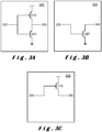
- Figure 3A shows a circuit of an inverter cell 300.
- the inverter cell 300 comprises a single PMOS transistor 310 that is coupled with a single NMOS transistor 320 sharing a single input 330.
- the input 330 is such that only one of the transistors 310, 320 is active at the same time.
- the inverter cell 300 also has an output 340.
- the input signal is '1' - in which case the PMOS transistor 310 is OFF and the NMOS transistor 320 is ON; and the input signal is '0' - in which case the PMOS transistor 310 is ON and the NMOS transistor 320 is OFF.
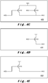
- Figure 4A shows a circuit of a negative-AND (NAND) cell 400.
- the NAND cell 400 comprises two PMOS transistors 410, 412 arranged in parallel and coupled to two NMOS transistor 420, 422 arranged in series.
- the NAND cell 400 also has an output 440.
- the PMOS transistor 410 and the NMOS transistor 420 share the same input 430, while the PMOS transistor 412 and the NMOS transistor 422 share the same input 432.
- the input 430 is such that only one of the transistors 410, 420 is active at the same time.
- Figure 4D shows the third input pattern of the NAND cell 400 (input 430 is '1' and input 432 is at '0').
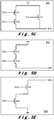
- Figure 5A shows a circuit of a more complex cell 500.
- the cell 500 comprises three PMOS transistors 510, 512, 514 and three NMOS transistor 520, 522, 524.
- the PMOS transistor 510 and the NMOS transistor 520 share the same input 530
- the PMOS transistor 512 and the NMOS transistor 522 share the same input 532
- the PMOS transistor 514 and the NMOS transistor 524 share the same input 534.
- PMOS transistors 510 and 512 are arranged in series but in parallel with PMOS transistor 514.
- the PMOS transistors are connected to NMOS transistor 524 which is in series with PMOS transistors 520 and 522 which are arranged in parallel.
- the cell 500 also has an output 540.
- the inputs 530, 532, 534 are such that only one of the coupled transistors 510, 520; 512, 522; 514, 524 are active at the same time.
- this cell 500 there are eight different input patterns possible:
- Figure 5D shows the sixth input pattern of the cell 500 (inputs 530, 532 are at '0' and input 534 is at '1').
- Figure 5E shows the seventh input pattern of the cell 500 (inputs 530, 534 are at '1' and input 532 is at '0').
- Figure 6A shows a detailed flowchart of how a variation factor of a basic structure is calculated, i.e. step 230 in the flowchart of Figure 2 .
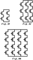
- the variation factor is determined for a limited number of basic elements; examples of which are illustrated in Figures 8A to 8K .
- the variation factor of a single PMOS transistor (illustrated in Figure 8B ) is determined. This can be achieved by using a Monte-Carlo simulation to determine a distribution of the delay of a signal when crossing the single PMOS transistor. From this distribution, the mean delay ⁇ and the standard deviation ⁇ can be determined. From these two values, the variation factor is known as the standard deviation divided by the mean delay, i.e. ⁇ / ⁇ .
- Such a Monte-Carlo simulation is done for each PVT corner. As such, for each PVT corner, the variation factor of a single PMOS transistor, denoted as ( ⁇ / ⁇ ) 1,1 , is determined.
- the variation factor is simulated for two serial PMOS transistors (illustrated in Figure 8C ), three serial PMOS transistors (illustrated in Figure 8D ), four serial PMOS transistors (illustrated in Figure 8E ), two parallel PMOS transistors, three parallel PMOS transistors, and four parallel PMOS transistors (not shown).
- Step 632 further comprises performing another seven Monte-Carlo simulations, for each PVT corner, to determine the variation factor of seven basic elements, i.e. a single NMOS transistor (illustrated in Figure 8A ), two, three and four serial NMOS transistors and two, three and four parallel NMOS transistors (illustrated in Figures 8F, 8G and 8H respectively), in each PVT corner.
- seven basic elements i.e. a single NMOS transistor (illustrated in Figure 8A ), two, three and four serial NMOS transistors and two, three and four parallel NMOS transistors (illustrated in Figures 8F, 8G and 8H respectively), in each PVT corner.
- the variation factor of a different number of basic elements is determined using Monte-Carlo simulations. For example, up to eight serial and/or parallel PMOS or NMOS transistors. Moreover, it would also be possible to determine the variation factor of mixed transistor combinations, e.g. two serial and two parallel PMOS transistors (illustrated in Figure 8I ), four serial and four parallel PMOS transistors (illustrated in Figure 8K ) or three serial and three parallel NMOS transistors (illustrated in Figure 8J ),.
- a basic structure can have three serial transistors, which may not be a basic element for which the variation factor was simulated.
- the variation factor of each basic structure can be determined using conventional simulation methods, but this is time-consuming and requires large amounts of computer resources.
- the variation factor of the basic structures is derived from the variation factor of the basic elements, which thus avoids having to perform numerous Monte-Carlo simulations.
- the variation factor of the basic elements are used to determine fitting parameters that enable the determination of the variation factor of basic structures without having to perform a Monte-Carlo estimation of the basic structure.
- the variation factor, ⁇ / ⁇ of a single transistor is inversely proportional to the square root of the area of the transistor. Therefore, when combining multiple transistors, i.e. effectively increasing the area of the transistors, this increased area can be linked to the variation factor.
- the fitting parameters ⁇ P , ⁇ S are determined in step 634 based on the variation factors of the basic elements. Specifically, for each PVT corner, a known fitting method is used to determine ⁇ P based on the variation factor of the single PMOS or NMOS transistor in combination with the two, four and eight parallel PMOS or NMOS transistors. Similarly, using the same known fitting method, the fitting parameter ⁇ S is determined for each PVT corner based on the variation factor of the single PMOS or NMOS transistor in combination with the two, four and eight serial PMOS or NMOS transistors.
- the known fitting methods may include least squares fitting or root-mean-square fitting.
- the variation factor of the basic structure can be determined. This is done in step 636 which uses as input the fitting parameters ⁇ P , ⁇ S , the variation factor of a single PMOS or NMOS transistor ( ⁇ / ⁇ ) 1,1 , and the number of active serial and/or parallel transistors in the basic structure N S , N P .
- These values in combination with equation (1) enable the determination of the variation factor of a basic structure by only using a limited number of Monte-Carlo estimations, e.g. fourteen, that determine the variation factor of the basic elements. This severely reduces the total simulation time that is needed to determine the variation factor of the basic structure, which, in turn, also decreases the time needed to determine the variation factor of the cell 100.
- determining the variation factor of the basic elements and the fitting parameters is done for each cell.
- the variation factor of the basic elements and the fitting parameters are only derived once for each PVT corner for both PMOS and NMOS transistors by using the same method as described above. After having determined these values, the variation factor of a single PMOS or NMOS transistor together with the fitting parameters are stored in a memory.
- Determining the variation factor of a basic structure then comprises retrieving the variation factor of a single PMOS or NMOS transistor ( ⁇ / ⁇ ) 1,1 and the fitting parameters ⁇ P , ⁇ S for the specific PVT corner of the cell 100 from the memory (step 635 in Figure 6B ), and calculating the variation factor of the basic structure in the same way as step 636 in Figure 6A described above.
- an input pattern comprises more than one basic structure, e.g. the input patterns illustrated in Figures 5B and 5C .
- the variation factor of one basic structure is determined first in the same way as step 636 in Figure 6A described above.
- the variation factor of the two parallel NMOS transistors 520, 522 is determined first; and, in Figure 5C , the variation factor of the two serial NMOS transistors 510, 512 is determined first. From this variation factor an PMOS or NMOS transistor with an equivalent size is determined, i.e. a single transistor which has a size such that it has a variation factor equal to the basic structure.
- the variation factor of the input pattern is then determined in the same way as step 636 in Figure 6A described above using the equivalent sized transistor with the other basic structure.
- the variation factor of two serial PMOS transistors i.e. transistor 524 and the equivalent transistor
- the variation factor of the two parallel NMOS transistors i.e. transistor 514 and the equivalent transistor
- the fitting parameters ⁇ P , ⁇ S are also dependent on the voltage and the temperature, i.e. ⁇ P (V,T), ⁇ S (V,T).
- the changes due to voltage and temperature are directly included in the fitting parameters. This has the advantage that fewer fitting parameters need to be stored in the memory. In particular, the fitting parameters only need to be stored depending on PMOS or NMOS transistors and the process of the transistor, i.e. the P value of the PVT corner.
- step 230 the end result of step 230 is that, for the cell 100, for each PVT corner, a variation factor has been determined for each possible input pattern.
- each cell 100 has, for each PVT corner, multiple variation factors.
- at least two variation factors as the inverter cell 300 is the simplest cell and has two basic structures.
- step 240 these multiple values are then used to determine a delay value for the cell, which is usually the maximum crossing time, but can also be the minimum crossing time or both. Details of step 240 are shown in Figure 7 .
- step 742 the highest value of the multiple variation factors is determined.
- the highest variation factor is chosen as this indicates the broadest variation range of the cell 100.
- average variation factors may also be used to determine average delay times.
- the variation factor of each input pattern is known, it is also possible to determine the expected delay for the most likely input pattern. Further, it would also be possible to determine the delay for each input pattern separately, in which case the AOCV table for the cell 100 includes very detailed information.
- step 250 the delay (which can be multiple values as described above), for each PVT corner, is stored in a multidimensional matrix, i.e. the AOCV table of the cell 100.
- the delay (which can be multiple values as described above), for each PVT corner, is stored in a multidimensional matrix, i.e. the AOCV table of the cell 100.
- the AOCV table of a cell 100 can easily be transferred and/or distributed.
- the method described above can also be used to determine the delay of entire cell libraries. Only the same basic elements need to be simulated from which the fitting parameters are determined.
- the fitting parameters in combination with the variation factor of a single NMOS or PMOS transistor are in turn used to determine the variation factor of the basic structures that form the various input patterns of various cells using equation 1. These are then used to determine the delay of the various cells that form the cell library.
- the AOCV table i.e. the multi-dimensional matrix containing the delay of the cell in various conditions, can then be grouped into a single AOCV file holding the delay information for the entire cell library.
- FIG. 9 shows a system 900 for executing the method described above.
- the system 900 comprises a processor 910; a memory 920; a variation factor simulation module 930; a fitting parameter derivation module 940; an input pattern determination module 950; a basic structure association module 960; a variation factor derivation module 970; and a delay derivation module 980.
- the modules 930, 940, 950, 960, 970, 980 may comprise computer-readable instructions that are executable by the processor 910 and are stored in the memory 920.
- the memory 920 comprises a basic elements module 922; a fitting parameter module 924; and an AOCV table 926.
- processor 910 may include numerous processors split over different machines and may also comprise cloud-computing resources.
- memory 920 may also comprises various fixed and/or removable components split over different machines and optionally also cloud-storage resources.
- the operation of the system 900 is as follows.
- the processor 910 retrieves the basic elements for which the variation factor needs to be simulated from the basic elements module 922 in the memory 920.
- the variation factor simulation module 930 then uses the processor 910 to simulate the variation factor for all the basic elements.
- the variation factor of a single NMOS or PMOS transistor, ( ⁇ / ⁇ ) 1,1 are then stored in the fitting parameter module 924 in the memory 920.
- the fitting parameter derivation module 940 uses the variation factors that were simulated in combination with a known fitting method to determine the fitting parameters, ⁇ P , ⁇ S , for each PVT corner for both NMOS and PMOS transistors, which fitting parameters, ⁇ P , ⁇ S , are then stored in the fitting parameter module 924 in the memory 920.
- the variation factor of a single NMOS or PMOS transistor and the fitting parameters, for each PVT corner need only be derived once.
- the input pattern determination module 950 will use the processor 910 to determine the possible input patterns of the cell and the basic structure association module 960 will associate each input pattern with at least one basic structure.
- the variation factor derivation module 970 uses the processor 910, derives the variation factor of each input pattern, for each PVT corner, by using equation (1).
- the delay derivation module 980 then uses the processor 910 to determine the delay, for each PVT corner, either the maximum, the minimum or both depending on the application, by using equations (2) and (3). The delay is then stored in the AOCV table 926 in the memory 920.
- the system 900 can be used to determine an AOCV table of an entire cell library.
- the memory 920 may also comprise an AOCV file that combines numerous AOCV tables.
Landscapes
- Engineering & Computer Science (AREA)
- Computer Hardware Design (AREA)
- Physics & Mathematics (AREA)
- Theoretical Computer Science (AREA)
- General Engineering & Computer Science (AREA)
- General Physics & Mathematics (AREA)
- Evolutionary Computation (AREA)
- Geometry (AREA)
- Microelectronics & Electronic Packaging (AREA)
- Design And Manufacture Of Integrated Circuits (AREA)
Priority Applications (2)
| Application Number | Priority Date | Filing Date | Title |
|---|---|---|---|
| EP16202854.2A EP3333734A1 (de) | 2016-12-08 | 2016-12-08 | Computerimplementiertes verfahren zur erzeugung einer advanced-on-chip-variation(aocv)-tabelle einer zelle und nichttransitorisches computerlesbares medium dafür |
| US15/835,214 US20180165395A1 (en) | 2016-12-08 | 2017-12-07 | Computer-implemented method for generating an advanced-on-chip-variation table of a cell and a non-transitory computer readable medium for doing the same |
Applications Claiming Priority (1)
| Application Number | Priority Date | Filing Date | Title |
|---|---|---|---|
| EP16202854.2A EP3333734A1 (de) | 2016-12-08 | 2016-12-08 | Computerimplementiertes verfahren zur erzeugung einer advanced-on-chip-variation(aocv)-tabelle einer zelle und nichttransitorisches computerlesbares medium dafür |
Publications (1)
| Publication Number | Publication Date |
|---|---|
| EP3333734A1 true EP3333734A1 (de) | 2018-06-13 |
Family
ID=57590301
Family Applications (1)
| Application Number | Title | Priority Date | Filing Date |
|---|---|---|---|
| EP16202854.2A Withdrawn EP3333734A1 (de) | 2016-12-08 | 2016-12-08 | Computerimplementiertes verfahren zur erzeugung einer advanced-on-chip-variation(aocv)-tabelle einer zelle und nichttransitorisches computerlesbares medium dafür |
Country Status (2)
| Country | Link |
|---|---|
| US (1) | US20180165395A1 (de) |
| EP (1) | EP3333734A1 (de) |
Citations (3)
| Publication number | Priority date | Publication date | Assignee | Title |
|---|---|---|---|---|
| US20080120584A1 (en) * | 2006-11-16 | 2008-05-22 | Clk Design Automation, Inc. | Timing variation characterization |
| US20100242007A1 (en) * | 2009-03-17 | 2010-09-23 | Kabushiki Kaisha Toshiba | Cell-library-for-statistical-timing-analysis creating apparatus and statistical-timing analyzing apparatus |
| US8656331B1 (en) * | 2013-02-14 | 2014-02-18 | Freescale Semiconductor, Inc. | Timing margins for on-chip variations from sensitivity data |
Family Cites Families (4)
| Publication number | Priority date | Publication date | Assignee | Title |
|---|---|---|---|---|
| US10255395B2 (en) * | 2016-03-11 | 2019-04-09 | Synopsys, Inc. | Analyzing delay variations and transition time variations for electronic circuits |
| US9881123B1 (en) * | 2016-06-30 | 2018-01-30 | Cadence Design Systems, Inc. | Method and system for timing analysis with adaptive timing window optimization for determining signal integrity impact |
| US10423742B2 (en) * | 2017-01-24 | 2019-09-24 | Synopsys, Inc. | Method to perform full accuracy hierarchical block level timing analysis with parameterized chip level contexts |
| US10622044B2 (en) * | 2017-09-22 | 2020-04-14 | Qualcomm Incorporated | Memory hold margin characterization and correction circuit |
-
2016
- 2016-12-08 EP EP16202854.2A patent/EP3333734A1/de not_active Withdrawn
-
2017
- 2017-12-07 US US15/835,214 patent/US20180165395A1/en not_active Abandoned
Patent Citations (3)
| Publication number | Priority date | Publication date | Assignee | Title |
|---|---|---|---|---|
| US20080120584A1 (en) * | 2006-11-16 | 2008-05-22 | Clk Design Automation, Inc. | Timing variation characterization |
| US20100242007A1 (en) * | 2009-03-17 | 2010-09-23 | Kabushiki Kaisha Toshiba | Cell-library-for-statistical-timing-analysis creating apparatus and statistical-timing analyzing apparatus |
| US8656331B1 (en) * | 2013-02-14 | 2014-02-18 | Freescale Semiconductor, Inc. | Timing margins for on-chip variations from sensitivity data |
Also Published As
| Publication number | Publication date |
|---|---|
| US20180165395A1 (en) | 2018-06-14 |
Similar Documents
| Publication | Publication Date | Title |
|---|---|---|
| US11663383B2 (en) | Method and system for hierarchical circuit simulation using parallel processing | |
| US8656331B1 (en) | Timing margins for on-chip variations from sensitivity data | |
| US20120123745A1 (en) | Adaptive Content-aware Aging Simulations | |
| TWI689833B (zh) | 調整用於靜態時序分析的時序降額的方法與電腦設備 | |
| US20100250187A1 (en) | Method and system for analyzing performance metrics of array type circuits under process variability | |
| US9690889B2 (en) | Method for adjusting a timing derate for static timing analysis | |
| KR20120047336A (ko) | 전자 회로의 계층적 오더 랭킹 시뮬레이션 방법 및 시뮬레이션을 위해 컴퓨터 실행가능 명령을 저장하는 컴퓨터 판독가능 기록 매체 | |
| US8397199B2 (en) | Versatile method and tool for simulation of aged transistors | |
| CN115398253A (zh) | 用于模拟缺陷可检测性分析的迅速且可扩展的方法 | |
| US8707234B1 (en) | Circuit noise extraction using forced input noise waveform | |
| US20090094569A1 (en) | Test pattern evaluation method and test pattern evaluation device | |
| US9734269B2 (en) | Liberty file generation | |
| US20150356229A1 (en) | Physical cell electromigration data generation | |
| US8635581B1 (en) | Method and apparatus for single event upset (SEU) detection and correction | |
| US9940418B2 (en) | Simulation of hierarchical circuit element arrays | |
| US9483599B1 (en) | Circuit design-specific failure in time rate for single event upsets | |
| US9177095B1 (en) | Methods, systems, and articles of manufacture for creating or manipulating electrical data sets for an electronic design | |
| US10140412B2 (en) | Timing matching method of timing analyzer and method of designing integrated circuit using the same | |
| US9582626B1 (en) | Using waveform propagation for accurate delay calculation | |
| EP3333734A1 (de) | Computerimplementiertes verfahren zur erzeugung einer advanced-on-chip-variation(aocv)-tabelle einer zelle und nichttransitorisches computerlesbares medium dafür | |
| US9235675B2 (en) | Multidimensional monte-carlo simulation for yield prediction | |
| US8593177B2 (en) | Integrated circuit with timing aware clock-tree and method for designing such an integrated circuit | |
| US8650021B2 (en) | Parallel flip-flop setup and hold timing analysis | |
| US6253356B1 (en) | System and method for improving logic synthesis in logic circuits | |
| US20180096087A1 (en) | Design method |
Legal Events
| Date | Code | Title | Description |
|---|---|---|---|
| PUAI | Public reference made under article 153(3) epc to a published international application that has entered the european phase |
Free format text: ORIGINAL CODE: 0009012 |
|
| STAA | Information on the status of an ep patent application or granted ep patent |
Free format text: STATUS: THE APPLICATION HAS BEEN PUBLISHED |
|
| AK | Designated contracting states |
Kind code of ref document: A1 Designated state(s): AL AT BE BG CH CY CZ DE DK EE ES FI FR GB GR HR HU IE IS IT LI LT LU LV MC MK MT NL NO PL PT RO RS SE SI SK SM TR |
|
| AX | Request for extension of the european patent |
Extension state: BA ME |
|
| STAA | Information on the status of an ep patent application or granted ep patent |
Free format text: STATUS: REQUEST FOR EXAMINATION WAS MADE |
|
| 17P | Request for examination filed |
Effective date: 20180625 |
|
| RBV | Designated contracting states (corrected) |
Designated state(s): AL AT BE BG CH CY CZ DE DK EE ES FI FR GB GR HR HU IE IS IT LI LT LU LV MC MK MT NL NO PL PT RO RS SE SI SK SM TR |
|
| RIC1 | Information provided on ipc code assigned before grant |
Ipc: G01R 31/28 20060101AFI20190107BHEP Ipc: G06F 17/50 20060101ALI20190107BHEP |
|
| GRAP | Despatch of communication of intention to grant a patent |
Free format text: ORIGINAL CODE: EPIDOSNIGR1 |
|
| STAA | Information on the status of an ep patent application or granted ep patent |
Free format text: STATUS: GRANT OF PATENT IS INTENDED |
|
| INTG | Intention to grant announced |
Effective date: 20190218 |
|
| STAA | Information on the status of an ep patent application or granted ep patent |
Free format text: STATUS: THE APPLICATION IS DEEMED TO BE WITHDRAWN |
|
| 18D | Application deemed to be withdrawn |
Effective date: 20190629 |