EP3331038A1 - Resistive random access memory and manufacturing method thereof - Google Patents
Resistive random access memory and manufacturing method thereof Download PDFInfo
- Publication number
- EP3331038A1 EP3331038A1 EP17204263.2A EP17204263A EP3331038A1 EP 3331038 A1 EP3331038 A1 EP 3331038A1 EP 17204263 A EP17204263 A EP 17204263A EP 3331038 A1 EP3331038 A1 EP 3331038A1
- Authority
- EP
- European Patent Office
- Prior art keywords
- layer
- electrode
- electrode layer
- data storage
- interconnection
- Prior art date
- Legal status (The legal status is an assumption and is not a legal conclusion. Google has not performed a legal analysis and makes no representation as to the accuracy of the status listed.)
- Withdrawn
Links
Images




Classifications
-
- H—ELECTRICITY
- H10—SEMICONDUCTOR DEVICES; ELECTRIC SOLID-STATE DEVICES NOT OTHERWISE PROVIDED FOR
- H10N—ELECTRIC SOLID-STATE DEVICES NOT OTHERWISE PROVIDED FOR
- H10N70/00—Solid-state devices having no potential barriers, and specially adapted for rectifying, amplifying, oscillating or switching
- H10N70/011—Manufacture or treatment of multistable switching devices
- H10N70/061—Shaping switching materials
- H10N70/066—Shaping switching materials by filling of openings, e.g. damascene method
-
- H—ELECTRICITY
- H10—SEMICONDUCTOR DEVICES; ELECTRIC SOLID-STATE DEVICES NOT OTHERWISE PROVIDED FOR
- H10N—ELECTRIC SOLID-STATE DEVICES NOT OTHERWISE PROVIDED FOR
- H10N70/00—Solid-state devices having no potential barriers, and specially adapted for rectifying, amplifying, oscillating or switching
- H10N70/011—Manufacture or treatment of multistable switching devices
-
- C—CHEMISTRY; METALLURGY
- C23—COATING METALLIC MATERIAL; COATING MATERIAL WITH METALLIC MATERIAL; CHEMICAL SURFACE TREATMENT; DIFFUSION TREATMENT OF METALLIC MATERIAL; COATING BY VACUUM EVAPORATION, BY SPUTTERING, BY ION IMPLANTATION OR BY CHEMICAL VAPOUR DEPOSITION, IN GENERAL; INHIBITING CORROSION OF METALLIC MATERIAL OR INCRUSTATION IN GENERAL
- C23C—COATING METALLIC MATERIAL; COATING MATERIAL WITH METALLIC MATERIAL; SURFACE TREATMENT OF METALLIC MATERIAL BY DIFFUSION INTO THE SURFACE, BY CHEMICAL CONVERSION OR SUBSTITUTION; COATING BY VACUUM EVAPORATION, BY SPUTTERING, BY ION IMPLANTATION OR BY CHEMICAL VAPOUR DEPOSITION, IN GENERAL
- C23C16/00—Chemical coating by decomposition of gaseous compounds, without leaving reaction products of surface material in the coating, i.e. chemical vapour deposition [CVD] processes
- C23C16/06—Chemical coating by decomposition of gaseous compounds, without leaving reaction products of surface material in the coating, i.e. chemical vapour deposition [CVD] processes characterised by the deposition of metallic material
-
- C—CHEMISTRY; METALLURGY
- C23—COATING METALLIC MATERIAL; COATING MATERIAL WITH METALLIC MATERIAL; CHEMICAL SURFACE TREATMENT; DIFFUSION TREATMENT OF METALLIC MATERIAL; COATING BY VACUUM EVAPORATION, BY SPUTTERING, BY ION IMPLANTATION OR BY CHEMICAL VAPOUR DEPOSITION, IN GENERAL; INHIBITING CORROSION OF METALLIC MATERIAL OR INCRUSTATION IN GENERAL
- C23C—COATING METALLIC MATERIAL; COATING MATERIAL WITH METALLIC MATERIAL; SURFACE TREATMENT OF METALLIC MATERIAL BY DIFFUSION INTO THE SURFACE, BY CHEMICAL CONVERSION OR SUBSTITUTION; COATING BY VACUUM EVAPORATION, BY SPUTTERING, BY ION IMPLANTATION OR BY CHEMICAL VAPOUR DEPOSITION, IN GENERAL
- C23C16/00—Chemical coating by decomposition of gaseous compounds, without leaving reaction products of surface material in the coating, i.e. chemical vapour deposition [CVD] processes
- C23C16/22—Chemical coating by decomposition of gaseous compounds, without leaving reaction products of surface material in the coating, i.e. chemical vapour deposition [CVD] processes characterised by the deposition of inorganic material, other than metallic material
- C23C16/30—Deposition of compounds, mixtures or solid solutions, e.g. borides, carbides, nitrides
- C23C16/34—Nitrides
-
- H—ELECTRICITY
- H10—SEMICONDUCTOR DEVICES; ELECTRIC SOLID-STATE DEVICES NOT OTHERWISE PROVIDED FOR
- H10N—ELECTRIC SOLID-STATE DEVICES NOT OTHERWISE PROVIDED FOR
- H10N70/00—Solid-state devices having no potential barriers, and specially adapted for rectifying, amplifying, oscillating or switching
- H10N70/20—Multistable switching devices, e.g. memristors
-
- H—ELECTRICITY
- H10—SEMICONDUCTOR DEVICES; ELECTRIC SOLID-STATE DEVICES NOT OTHERWISE PROVIDED FOR
- H10N—ELECTRIC SOLID-STATE DEVICES NOT OTHERWISE PROVIDED FOR
- H10N70/00—Solid-state devices having no potential barriers, and specially adapted for rectifying, amplifying, oscillating or switching
- H10N70/20—Multistable switching devices, e.g. memristors
- H10N70/231—Multistable switching devices, e.g. memristors based on solid-state phase change, e.g. between amorphous and crystalline phases, Ovshinsky effect
-
- H—ELECTRICITY
- H10—SEMICONDUCTOR DEVICES; ELECTRIC SOLID-STATE DEVICES NOT OTHERWISE PROVIDED FOR
- H10N—ELECTRIC SOLID-STATE DEVICES NOT OTHERWISE PROVIDED FOR
- H10N70/00—Solid-state devices having no potential barriers, and specially adapted for rectifying, amplifying, oscillating or switching
- H10N70/20—Multistable switching devices, e.g. memristors
- H10N70/25—Multistable switching devices, e.g. memristors based on bulk electronic defects, e.g. trapping of electrons
-
- H—ELECTRICITY
- H10—SEMICONDUCTOR DEVICES; ELECTRIC SOLID-STATE DEVICES NOT OTHERWISE PROVIDED FOR
- H10N—ELECTRIC SOLID-STATE DEVICES NOT OTHERWISE PROVIDED FOR
- H10N70/00—Solid-state devices having no potential barriers, and specially adapted for rectifying, amplifying, oscillating or switching
- H10N70/801—Constructional details of multistable switching devices
- H10N70/821—Device geometry
- H10N70/826—Device geometry adapted for essentially vertical current flow, e.g. sandwich or pillar type devices
-
- H—ELECTRICITY
- H10—SEMICONDUCTOR DEVICES; ELECTRIC SOLID-STATE DEVICES NOT OTHERWISE PROVIDED FOR
- H10N—ELECTRIC SOLID-STATE DEVICES NOT OTHERWISE PROVIDED FOR
- H10N70/00—Solid-state devices having no potential barriers, and specially adapted for rectifying, amplifying, oscillating or switching
- H10N70/801—Constructional details of multistable switching devices
- H10N70/841—Electrodes
Definitions
- the present invention relates to the field of semiconductor technologies, and in particular, to a Resistive Random Access Memory (RRAM) and a manufacturing method thereof.
- RRAM Resistive Random Access Memory
- Non-Volatile Memory NVM
- the RRAM has increasingly attracted attention, and such a memory has provided many advantages, including structural simplicity, low power consumption, fast operation, high level of integration, and so on. Selection of a suitable electrode is key to the manufacturing and operation of an RRAM device.
- a bottom electrode (BE) of a RRAM unit may be processed in a Back End Of Line (BEOL) stage. It is preferable that the BE material possesses sufficient gap filling capability.
- a TiN film formed through a Physical Vapor Deposition (PVD) process provides an electrode most researched and commonly used for BE in a RRAM device because the TiN film has excellent electric performance.
- the TiN film formed through PVD process has a poor gap filling capability.
- a deposition process using a higher voltage DC power source and AC bias power source is required.
- TiN film deposited in such a way may possess an improved gap filling capability. It is, however, subject to peeling. That is, such a TiN film is easy to peel off from a chip.
- a current research result shows that a bottom electrode TiN film has a relatively high compressive stress of about -3000 to -7000 MPa.
- the peeling issues occur in a later TiN deposition process and become worse with extension of the time, and are more serious at edges of the chip. Therefore, it is necessary to balance the tradeoff between gap filling capability and the peeling issues.
- a method for manufacturing a RRAM including: providing a bottom interconnection layer; forming a bottom dielectric layer above the bottom interconnection layer, the bottom dielectric layer comprising a via though the bottom dielectric layer that exposes a portion of the bottom interconnection layer; and forming a bottom electrode layer in the via, the bottom electrode layer including a first electrode selectively grown above the bottom interconnection layer.
- the material of the first electrode includes: cobalt or ruthenium.
- the first electrode is selectively grown above the bottom interconnection layer using a chemical vapor deposition (CVD) process.
- CVD chemical vapor deposition
- the CVD process includes: introducing reaction gas C 7 H 5 CoO 2 with a gas flow from 10 sccm to 50 sccm in a reaction chamber, within a temperature range from 100°C to 300°C, and within a pressure range from 0.1 Torr to 100 Torr.
- the bottom electrode layer further includes: a second electrode above the first electrode.
- the second electrode includes: titanium nitride, tantalum nitride, or tungsten nitride.
- thickness of the second electrode is less than a thickness of the first electrode.
- the thickness of the second electrode is 30 ⁇ to 250 ⁇ ; and the thickness of the first electrode is 320 ⁇ to 620 ⁇ .
- the thickness of the bottom electrode layer is 350 ⁇ to 650 ⁇ .
- the step of forming a bottom electrode layer in the via includes: depositing, above the bottom interconnection layer, a first electrode that selectively grows on the bottom interconnection layer and fills a part of the via; forming a second electrode above the bottom dielectric layer and above the first electrode; and performing planarization on the second electrode to remove a part of the second electrode above the bottom dielectric layer.
- the method further includes: forming a data storage layer above the bottom electrode layer; and forming a top electrode layer above the data storage layer.
- the data storage layer includes: a switch layer above the bottom electrode layer and an glue layer above the switch layer; wherein the top electrode layer is formed above the glue layer.
- the top electrode layer includes: a metal electrode layer above the data storage layer and a top protection layer above the metal electrode layer.
- the metal electrode layer includes: aluminum; and the top protection layer includes: titanium nitride, tantalum nitride, or tungsten nitride.
- the method further includes: forming a patterned hard mask layer above the top electrode layer; using the patterned hard mask layer as a mask to etch the top electrode layer and the data storage layer to form a patterned top electrode layer and a patterned data storage layer below the patterned hard mask layer; removing the patterned hard mask layer; forming a barrier layer to cover the patterned top electrode layer and the patterned data storage layer; and forming a top interconnection layer that penetrates the barrier layer and connects with the top electrode layer.
- the bottom electrode layer includes a first electrode that is selectively grown, thus having a better via filling capability.
- the second electrode can prevent the first electrode from oxidation.
- the second electrode is not prone to peeling issues.
- a RRAM including: a bottom interconnection layer; a bottom electrode layer above the bottom interconnection layer, the bottom electrode layer including a first electrode selectively grown above the bottom interconnection layer; and a bottom dielectric layer surrounding the bottom electrode layer.
- the first electrode includes: cobalt or ruthenium.
- the bottom electrode layer further includes: a second electrode above the first electrode.
- the second electrode includes: titanium nitride, tantalum nitride, or tungsten nitride.
- thickness of the second electrode is less than a thickness of the first electrode.
- a thickness of the second electrode is 30 ⁇ to 250 ⁇ ; and the thickness of the first electrode is 320 ⁇ to 620 ⁇ .
- the thickness of the bottom electrode layer is 350 ⁇ to 650 ⁇ .
- the RRAM further includes: a data storage layer above the bottom electrode layer; and a top electrode layer above the data storage layer.
- the data storage layer includes: a switch layer positioned above the bottom electrode layer and a glue layer positioned above the switch layer; wherein the top electrode layer is formed above the glue layer.
- the top electrode layer includes: a metal electrode layer positioned above the data storage layer and a top protection layer positioned above the metal electrode layer.
- the metal electrode layer includes: aluminum; and the top protection layer includes: titanium nitride, tantalum nitride, or tungsten nitride.
- the RRAM further includes: a top interconnection layer positioned above the top electrode layer; and a barrier layer surrounding the top electrode layer, the data storage layer, and the top interconnection layer.
- the bottom electrode layer includes a first electrode that selectively grows, thus having a better via filling capability.
- the second electrode can prevent the first electrode from oxidation.
- the second electrode is not prone to peeling issues.
- a RRAM according to the second aspect of the present invention may be obtained by a method according to the first aspect of the present invention.
- Fig. 1 is a flowchart of a manufacturing method of a RRAM.
- a bottom interconnection layer is provided.
- the material of the bottom interconnection layer may include copper and the like.
- step S102 A bottom dielectric layer is formed above the bottom interconnection layer, the bottom dielectric layer having a via that exposes a portion of the bottom interconnection layer and provides connection access to the bottom interconnection layer.
- the step S102 may include: forming a bottom dielectric layer above the bottom interconnection layer; and etching through the bottom dielectric layer to form a via that exposes the bottom interconnection layer.
- a bottom electrode layer is formed or deposited in the via, the bottom electrode layer including a first electrode that is selectively grown above the bottom interconnection layer.
- the term "selectively grown" here means that the first electrode is formed above the bottom interconnection layer, but is not formed above the bottom dielectric layer.
- a conductive material matching lattice spacing or lattice constant of the material of the bottom interconnection layer may be selected as the first electrode.
- the material of the first electrode may include: Co or Ru or the like.
- the thickness of the first electrode may be 320 ⁇ to 620 ⁇ (such as 400 ⁇ , 500 ⁇ or 550 ⁇ ).
- the first electrode may be selectively grown above the bottom interconnection layer by using a CVD process. This can ensure that the first electrode grows above the bottom interconnection layer, and thus can achieve a better filling of the via (i.e., gap filling capability).
- the CVD process may be carried out under the following condition: introducing reaction gas C 7 H 5 CoO 2 (CyclopentadienylCobalt Dicarbonyl) with a gas flow from 10 sccm to 50 sccm (for example, the gas flow may be 20 sccm, 30 sccm, or 40 sccm) in a reaction chamber, within a temperature range from 100°C to 300°C (e.g., at a temperature of 200°C or 250°C), and within a pressure range from 0.1 Torr to 100 Torr (e.g., at a pressure of 10 Torr, 30 Torr or 70 Torr).
- the term "sccm” is a flow unit and stands for "standard cubic centimeters per minute".
- C 7 H 5 CoO 2 has good wettability, and can thus help improve the gap filling capability of Co.
- the Co film formed through the CVD process has a lower resistance, and can ensure a better filling property.
- the Co film formed through CVD has a higher growth selectivity on the bottom interconnection layer. Relative to the bottom dielectric layer around it, it is easier for the Co film to grow on a surface of the bottom interconnection layer (e.g., copper), leading to improved gap filling.
- depositing, above the bottom interconnection layer, the first electrode that selectively grows on the bottom interconnection layer can help improve the via filling capability of the bottom electrode layer.
- the bottom electrode layer may further include: a second electrode above the first electrode.
- the second electrode may be used as an oxidation barrier layer to prevent the first electrode from oxidation.
- the material of the second electrode may include: TiN, TaN or WN or the like. These materials are conductive electrically and thus can play the role of the second electron in addition to helping prevent the first electrode from oxidation.
- the thickness of the second electrode is less than that of the first electrode.
- the thickness of the second electrode may be 30 ⁇ to 250 ⁇ (e.g., 50 ⁇ , 100 ⁇ or 200 ⁇ ).
- the via is filled with the first electrode, the thickness of the second electrode subsequently filled is thinner. As a result, peeling issues are less likely to occur. Reliability of the device may thus be improved.
- the thickness of the bottom electrode layer i.e., the sum of the thicknesses of the first electrode and the second electrode
- the thickness of the bottom electrode layer may be 350 ⁇ to 650 ⁇ (e.g., 500 ⁇ ).
- the manufacturing method above may further include: forming a data storage layer above the bottom electrode layer.
- the data storage layer may be formed above the second electrode.
- the manufacturing method above may further include: forming a top electrode layer above the data storage layer.
- the data storage layer and the top electrode layer here may be patterned.
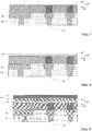
- Fig. 2 to Fig. 14 are cross-sectional views schematically showing a PRAM structure during various manufacturing stage. The manufacturing process of a RRAM according to a form of the present invention is described below in detail with reference to Fig. 2 to Fig. 14 .
- a bottom interconnection layer 210 is provided.
- the material of the bottom interconnection layer may be copper.
- the bottom interconnection layer 210 may be surrounded by a first dielectric layer 202.
- the material of the first dielectric layer 202 may include silicon dioxide.
- Fig. 2 further illustrates a metal interconnection structure 201 of a logic unit part.
- a bottom dielectric layer 220 is formed above the bottom interconnection layer 210 and the first dielectric layer 202.
- the material of the bottom dielectric layer 220 may include: Nitrogen Doped SiC (NDC), silicon nitride and/or silicon dioxide.
- the bottom dielectric layer 220 may include: a NDC layer above the bottom interconnection layer 210, a silicon nitride layer above the NDC layer, and a silicon dioxide layer above the silicon nitride layer.
- the thickness of the NDC layer may be 300 ⁇ to 400 ⁇ (e.g., 380 ⁇ ).
- the thickness of the silicon nitride layer for example, may be 200 ⁇ to 350 ⁇ (e.g., 300 ⁇ ).
- the thickness of the silicon dioxide layer for example, may be 30 ⁇ to 100 ⁇ (e.g., 50 ⁇ ).
- the bottom dielectric layer 220 is etched to form at least one via 230 that exposes a portion of the bottom interconnection layer 210.
- a bottom electrode layer is formed or deposited in the via 230.
- the process of forming the bottom electrode layer is described below in detail with reference to Fig. 5 to Fig. 7 .
- a first electrode 241 that selectively grows and fills a part of the via 230 is formed above the bottom interconnection layer 210.
- the first electrode 241 may be selectively grown above the bottom interconnection layer 210 by using a CVD process.
- the first electrode 241 selectively grown is formed above the bottom interconnection layer 210, but is not formed above the bottom dielectric layer 220. As such, a better filling of the via can be achieved.
- a second electrode 242 is formed above the bottom dielectric layer 220 and above the first electrode 241 through a PVD or Atomic Layer Deposition (ALD) process.
- the second electrode 242 fills the remaining part of the via 230.
- planarization e.g., Chemical Mechanical Planarization (CMP) is carried out on the second electrode 242 to remove a part of the second electrode 242 above the bottom dielectric layer 220. That is, a part of the second electrode outside the via 230 is removed through a planarization process.
- CMP Chemical Mechanical Planarization
- the bottom electrode layer 240 in the via 230 is formed, and the bottom electrode layer 240 may include the first electrode 241 and the second electrode 242.
- a data storage layer 260 is formed above the bottom electrode layer 240.
- the data storage layer 260 is formed above the second electrode 242 and the bottom dielectric layer 220.
- the data storage layer 260 may include: a switch layer (SL) above the bottom electrode layer 240 and a glue layer (GL) (not shown) above the SL.
- a top electrode layer (formed in a subsequent step) is formed above the GL.
- the SL and the GL may each be used as the data storage layer.
- the material of the SL may include a-Si (amorphous silicon), and the material of the GL may include silicon nitride.
- the top electrode layer 270 may include: a metal electrode layer 271 above the data storage layer 260 and a top protection layer 272 above the metal electrode layer 271.
- the material of the metal electrode layer 271 may include: Al or the like.
- the material of the top protection layer 272 may include: titanium nitride, tantalum nitride, or tungsten nitride or the like. The top protection layer may prevent the metal electrode layer from oxidation.
- the manufacturing method of a RRAM above may further include the following steps.
- a patterned hard mask layer 280 may be formed above the top electrode layer 270 (e.g., above the top protection layer 272 of the top electrode layer 270).
- the patterned hard mask layer 280 is used as a mask to etch the top electrode layer 270 and the data storage layer 260 to form a patterned top electrode layer 270 and a patterned data storage layer 260.
- the hard mask layer 280 is removed.
- a barrier layer 310 is formed to cover the patterned top electrode layer 270 and the patterned data storage layer 260 from the top and the sides.
- the barrier layer is formed above and on two or more sides of the top electrode layer 270 and also formed on two or more sides of the data storage layer 260.
- the barrier layer 310 may include: a NDC layer above and on sides of the top electrode layer 270 and on sides of the data storage layer 260, and a BD layer above the NDC layer.
- the BD layer is a Black Diamond SiOCH, which is a low dielectric constant material.
- the thickness of the NDC layer may be 100 ⁇ to 200 ⁇ (e.g., 150 ⁇ ), and the thickness of the BD layer may be 300 ⁇ to 400 ⁇ (e.g., 350 ⁇ ).
- a top interconnection layer 320 that penetrates the barrier layer 310 and connects with the top electrode layer 270 is formed.
- the material of the top interconnection layer may include copper.
- the step of forming the top interconnection layer may include: etching the barrier layer 310 to form an opening that exposes an upper surface of the top electrode layer 270 (e.g., an upper surface of the top protection layer 272 of the top electrode layer 270); and then forming, in the opening, a top interconnection layer 320 in contact with the top electrode layer 270 (e.g., in contact with the top protection layer 272 of the top electrode layer 270).
- the manufacturing method of RRAM above may be used to improve the via filling capability above the bottom electrode layer.
- the resulting electrodes are not prone to peeling. As such, reliability of the resulting device can be improved.
- a RRAM may be formed with the manufacturing method described above.
- the RRAM may include a bottom interconnection layer 210.
- the material of the bottom interconnection layer 210 may include copper.
- the RRAM may further include a bottom electrode layer 240 above the bottom interconnection layer 210.
- the bottom electrode layer 240 may include a first electrode 241 selectively grown on the bottom interconnection layer 210.
- the material of the first electrode 241 may include, for example, Co or Ru or the like.
- the thickness of the first electrode may be 320 ⁇ to 620 ⁇ (such as 400 ⁇ , 500 ⁇ or 550 ⁇ ).
- the RRAM may further include a bottom dielectric layer 220 that surrounds the bottom electrode layer 240.
- the first electrode selectively grown has a relatively good gap filling capability with respect to filing the via.
- the bottom electrode layer 240 may further include: a second electrode 242 above the first electrode 241.
- the second electrode may prevent the first electrode from oxidation.
- the material of the second electrode 242 may include: titanium nitride, tantalum nitride, or tungsten nitride or the like.
- the thickness of the second electrode 242 is less than that of the first electrode 241.
- the thickness of the second electrode 242 may be 30 ⁇ to 250 ⁇ (e.g., 50 ⁇ , 100 ⁇ or 200 ⁇ ). As the second electrode is thinner, peeling issues are unlikely to occur, and reliability of the device can be improved.
- the thickness of the bottom electrode layer i.e., the sum of the thicknesses of the first electrode and the second electrode
- the thickness of the bottom electrode layer maybe 350 ⁇ to 650 ⁇ (e.g., 500 ⁇ ).
- the RRAM may further include a data storage layer 260 above the bottom electrode layer 240.
- the data storage layer 260 may be above the second electrode 242.
- the RRAM may further include a top electrode layer 270 above the data storage layer 260.
- the data storage layer 260 may include: a SL above the bottom electrode layer 240 and a GL (not shown) above the SL.
- the top electrode layer 270 is above the GL.
- the SL and the GL may each be used as the data storage layer.
- the top electrode layer 270 may include: a metal electrode layer 271 above the data storage layer 260 and a top protection layer 272 above the metal electrode layer 271.
- the material of the metal electrode layer 271 may include Al or the like.
- the material of the top protection layer 272 may include: titanium nitride, tantalum nitride, or tungsten nitride or the like. The top protection layer may prevent the metal electrode layer from oxidation.
- the RRAM may further include: a top interconnection layer 320 above the top electrode layer 270.
- the material of the top interconnection layer 320 may include copper or the like.
- the RRAM may further include: a barrier layer 310 that surrounds the top electrode layer 270, the data storage layer 260, and the top interconnection layer 320.
- the bottom electrode layer (including the first electrode 241 and the second electrode 242) of the RRAM of the present invention provides an improved capability for filing the via, and is not prone to peeling. As such, reliability of the device RRAM device above can be improved.
- the present invention has described the process of manufacturing an RRAM structure and the resulting device in detail. In order to avoid obscuring the concept of the present invention, some well-known details in the field are omitted. Those of ordinary skill in the art should understand according to the above description how the technical solutions disclosed here are implemented.
Landscapes
- Chemical & Material Sciences (AREA)
- Engineering & Computer Science (AREA)
- Manufacturing & Machinery (AREA)
- General Chemical & Material Sciences (AREA)
- Chemical Kinetics & Catalysis (AREA)
- Materials Engineering (AREA)
- Mechanical Engineering (AREA)
- Metallurgy (AREA)
- Organic Chemistry (AREA)
- Inorganic Chemistry (AREA)
- Semiconductor Memories (AREA)
Abstract
Description
- The present application is based on and claims priority to Chinese Patent Application
CN201611074755.1, filed November 30, 2016 - The present invention relates to the field of semiconductor technologies, and in particular, to a Resistive Random Access Memory (RRAM) and a manufacturing method thereof.
- Among various types of Non-Volatile Memory (NVM), the RRAM has increasingly attracted attention, and such a memory has provided many advantages, including structural simplicity, low power consumption, fast operation, high level of integration, and so on. Selection of a suitable electrode is key to the manufacturing and operation of an RRAM device.
- A bottom electrode (BE) of a RRAM unit may be processed in a Back End Of Line (BEOL) stage. It is preferable that the BE material possesses sufficient gap filling capability. A TiN film formed through a Physical Vapor Deposition (PVD) process provides an electrode most researched and commonly used for BE in a RRAM device because the TiN film has excellent electric performance. However, the TiN film formed through PVD process has a poor gap filling capability. In order to improve the gap filling capability of TiN, a deposition process using a higher voltage DC power source and AC bias power source is required. TiN film deposited in such a way may possess an improved gap filling capability. It is, however, subject to peeling. That is, such a TiN film is easy to peel off from a chip. A current research result shows that a bottom electrode TiN film has a relatively high compressive stress of about -3000 to -7000 MPa. The peeling issues occur in a later TiN deposition process and become worse with extension of the time, and are more serious at edges of the chip. Therefore, it is necessary to balance the tradeoff between gap filling capability and the peeling issues.
- It is an object of the present invention to provide a method for manufacturing a RRAM and a corresponding RRAM in which one or more of the above discussed problems in the prior art may be solved.
- The object is achieved by the features of the respective independent claims. Further embodiments and developments are defined in the dependent claims.
- According to a first aspect of the present invention, a method for manufacturing a RRAM is provided, including: providing a bottom interconnection layer; forming a bottom dielectric layer above the bottom interconnection layer, the bottom dielectric layer comprising a via though the bottom dielectric layer that exposes a portion of the bottom interconnection layer; and forming a bottom electrode layer in the via, the bottom electrode layer including a first electrode selectively grown above the bottom interconnection layer.
- Preferably, the material of the first electrode includes: cobalt or ruthenium.
- Preferably, the first electrode is selectively grown above the bottom interconnection layer using a chemical vapor deposition (CVD) process.
- Preferably, the CVD process includes: introducing reaction gas C7H5CoO2 with a gas flow from 10 sccm to 50 sccm in a reaction chamber, within a temperature range from 100°C to 300°C, and within a pressure range from 0.1 Torr to 100 Torr.
- Preferably, the bottom electrode layer further includes: a second electrode above the first electrode.
- Preferably, the second electrode includes: titanium nitride, tantalum nitride, or tungsten nitride.
- Preferably, thickness of the second electrode is less than a thickness of the first electrode.
- Preferably, the thickness of the second electrode is 30Å to 250Å; and the thickness of the first electrode is 320Å to 620Å.
- Preferably, the thickness of the bottom electrode layer is 350Å to 650Å.
- Preferably, the step of forming a bottom electrode layer in the via includes: depositing, above the bottom interconnection layer, a first electrode that selectively grows on the bottom interconnection layer and fills a part of the via; forming a second electrode above the bottom dielectric layer and above the first electrode; and performing planarization on the second electrode to remove a part of the second electrode above the bottom dielectric layer.
- Preferably, the method further includes: forming a data storage layer above the bottom electrode layer; and forming a top electrode layer above the data storage layer.
- Preferably, the data storage layer includes: a switch layer above the bottom electrode layer and an glue layer above the switch layer; wherein the top electrode layer is formed above the glue layer.
- Preferably, the top electrode layer includes: a metal electrode layer above the data storage layer and a top protection layer above the metal electrode layer.
- Preferably, the metal electrode layer includes: aluminum; and the top protection layer includes: titanium nitride, tantalum nitride, or tungsten nitride.
- Preferably, the method further includes: forming a patterned hard mask layer above the top electrode layer; using the patterned hard mask layer as a mask to etch the top electrode layer and the data storage layer to form a patterned top electrode layer and a patterned data storage layer below the patterned hard mask layer; removing the patterned hard mask layer; forming a barrier layer to cover the patterned top electrode layer and the patterned data storage layer; and forming a top interconnection layer that penetrates the barrier layer and connects with the top electrode layer.
- Preferably, the bottom electrode layer includes a first electrode that is selectively grown, thus having a better via filling capability.
- Preferably, the second electrode can prevent the first electrode from oxidation.
- Preferably, the second electrode is not prone to peeling issues.
- According to a second aspect of the present invention, a RRAM is provided, including: a bottom interconnection layer; a bottom electrode layer above the bottom interconnection layer, the bottom electrode layer including a first electrode selectively grown above the bottom interconnection layer; and a bottom dielectric layer surrounding the bottom electrode layer.
- Preferably, the first electrode includes: cobalt or ruthenium.
- Preferably, the bottom electrode layer further includes: a second electrode above the first electrode.
- Preferably, the second electrode includes: titanium nitride, tantalum nitride, or tungsten nitride.
- Preferably, thickness of the second electrode is less than a thickness of the first electrode.
- Preferably, a thickness of the second electrode is 30Å to 250Å; and the thickness of the first electrode is 320Å to 620Å.
- Preferably, the thickness of the bottom electrode layer is 350Å to 650Å.
- Preferably, the RRAM further includes: a data storage layer above the bottom electrode layer; and a top electrode layer above the data storage layer.
- Preferably, the data storage layer includes: a switch layer positioned above the bottom electrode layer and a glue layer positioned above the switch layer; wherein the top electrode layer is formed above the glue layer.
- Preferably, the top electrode layer includes: a metal electrode layer positioned above the data storage layer and a top protection layer positioned above the metal electrode layer.
- Preferably, the metal electrode layer includes: aluminum; and the top protection layer includes: titanium nitride, tantalum nitride, or tungsten nitride.
- Preferably, the RRAM further includes: a top interconnection layer positioned above the top electrode layer; and a barrier layer surrounding the top electrode layer, the data storage layer, and the top interconnection layer.
- Preferably, the bottom electrode layer includes a first electrode that selectively grows, thus having a better via filling capability.
- Preferably, the second electrode can prevent the first electrode from oxidation.
- Preferably, the second electrode is not prone to peeling issues.
- A RRAM according to the second aspect of the present invention may be obtained by a method according to the first aspect of the present invention.
- Other features of the present invention and advantages thereof will become clear through the following detailed description made about exemplary forms of the present invention with reference to accompanying drawings.
- The accompanying drawings, which form a part of the specification, describe forms of the present invention, and are used for explain the principle of the present invention along with the specification.
- The present invention may be understood more clearly according to the following detailed descriptions made with reference to the accompanying drawings, in which:
-
Fig. 1 is a flowchart of a manufacturing method of a RRAM; and -
Figs. 2-14 are cross-sectional views schematically showing a RRAM structure during various manufacturing stages. - Various exemplary forms of the present invention will now be described in detail with reference to the accompanying drawings. It should be noted that, unless otherwise specifically indicated, relative arrangement of the components and the steps, numerical expressions and values stated in the forms do not limit the present invention.
- At the same time, it should be understood that, for ease of description, sizes of various parts shown in the drawings are not drawn according to an actual proportional relation.
- The following description about at least one exemplary form is merely explanatory, and is by no means any limitation to the present invention and applications or use thereof.
- Technologies, methods and devices known to those of ordinary skill in the art may not be discussed in detail. But in suitable cases, these technologies, methods and devices should be regarded as a part of the description.
- In all examples shown and discussed here, any specific value should be explained as merely exemplary instead of limiting. Therefore, other examples of the exemplary forms may have different values.
- It should be noted that similar reference signs, labels, numerals, and letters indicate similar items in the following drawings. Therefore, once an item is defined in one drawing, it is not necessary to further discuss it in the subsequent drawings.
-
Fig. 1 is a flowchart of a manufacturing method of a RRAM. - In step S101, a bottom interconnection layer is provided. As an example, the material of the bottom interconnection layer may include copper and the like.
- In step S102. A bottom dielectric layer is formed above the bottom interconnection layer, the bottom dielectric layer having a via that exposes a portion of the bottom interconnection layer and provides connection access to the bottom interconnection layer. For example, the step S102 may include: forming a bottom dielectric layer above the bottom interconnection layer; and etching through the bottom dielectric layer to form a via that exposes the bottom interconnection layer.
- In step S103. A bottom electrode layer is formed or deposited in the via, the bottom electrode layer including a first electrode that is selectively grown above the bottom interconnection layer. It should be noted that the term "selectively grown" here means that the first electrode is formed above the bottom interconnection layer, but is not formed above the bottom dielectric layer. For example, a conductive material matching lattice spacing or lattice constant of the material of the bottom interconnection layer may be selected as the first electrode. For example, in a situation where the bottom interconnection layer is copper, the material of the first electrode may include: Co or Ru or the like. In one implementation, the thickness of the first electrode may be 320Å to 620Å (such as 400Å, 500Å or 550Å).
- In a form, the first electrode may be selectively grown above the bottom interconnection layer by using a CVD process. This can ensure that the first electrode grows above the bottom interconnection layer, and thus can achieve a better filling of the via (i.e., gap filling capability).
- By taking deposition of a Co film as an example, the CVD process may be carried out under the following condition: introducing reaction gas C7H5CoO2 (CyclopentadienylCobalt Dicarbonyl) with a gas flow from 10 sccm to 50 sccm (for example, the gas flow may be 20 sccm, 30 sccm, or 40 sccm) in a reaction chamber, within a temperature range from 100°C to 300°C (e.g., at a temperature of 200°C or 250°C), and within a pressure range from 0.1 Torr to 100 Torr (e.g., at a pressure of 10 Torr, 30 Torr or 70 Torr). The term "sccm" is a flow unit and stands for "standard cubic centimeters per minute". C7H5CoO2 has good wettability, and can thus help improve the gap filling capability of Co.
- The Co film formed through the CVD process has a lower resistance, and can ensure a better filling property. The Co film formed through CVD has a higher growth selectivity on the bottom interconnection layer. Relative to the bottom dielectric layer around it, it is easier for the Co film to grow on a surface of the bottom interconnection layer (e.g., copper), leading to improved gap filling.
- In the form above, depositing, above the bottom interconnection layer, the first electrode that selectively grows on the bottom interconnection layer can help improve the via filling capability of the bottom electrode layer.
- In a form, the bottom electrode layer may further include: a second electrode above the first electrode. The second electrode may be used as an oxidation barrier layer to prevent the first electrode from oxidation. For example, the material of the second electrode may include: TiN, TaN or WN or the like. These materials are conductive electrically and thus can play the role of the second electron in addition to helping prevent the first electrode from oxidation. Preferably, the thickness of the second electrode is less than that of the first electrode. For example, the thickness of the second electrode may be 30Å to 250Å (e.g., 50Å, 100Å or 200Å).
- Because the via is filled with the first electrode, the thickness of the second electrode subsequently filled is thinner. As a result, peeling issues are less likely to occur. Reliability of the device may thus be improved.
- In a form, the thickness of the bottom electrode layer (i.e., the sum of the thicknesses of the first electrode and the second electrode) may be 350Å to 650Å (e.g., 500Å).
- Optionally, the manufacturing method above may further include: forming a data storage layer above the bottom electrode layer. For example, the data storage layer may be formed above the second electrode. Optionally, the manufacturing method above may further include: forming a top electrode layer above the data storage layer. In a form, the data storage layer and the top electrode layer here may be patterned.
-
Fig. 2 to Fig. 14 are cross-sectional views schematically showing a PRAM structure during various manufacturing stage. The manufacturing process of a RRAM according to a form of the present invention is described below in detail with reference toFig. 2 to Fig. 14 . - Firstly, as shown in
Fig. 2 , abottom interconnection layer 210 is provided. For example, the material of the bottom interconnection layer may be copper. In a form, thebottom interconnection layer 210 may be surrounded by a firstdielectric layer 202. For example, the material of thefirst dielectric layer 202 may include silicon dioxide. As an example,Fig. 2 further illustrates ametal interconnection structure 201 of a logic unit part. - Next, as shown in
Fig. 3 , abottom dielectric layer 220 is formed above thebottom interconnection layer 210 and thefirst dielectric layer 202. - In a form, the material of the
bottom dielectric layer 220 may include: Nitrogen Doped SiC (NDC), silicon nitride and/or silicon dioxide. For example, thebottom dielectric layer 220 may include: a NDC layer above thebottom interconnection layer 210, a silicon nitride layer above the NDC layer, and a silicon dioxide layer above the silicon nitride layer. The thickness of the NDC layer, for example, may be 300Å to 400Å (e.g., 380Å). The thickness of the silicon nitride layer, for example, may be 200 Å to 350 Å (e.g., 300Å). The thickness of the silicon dioxide layer, for example, may be 30 Å to 100 Å (e.g., 50Å). - Next, as shown in
Fig. 4 , through, e.g., a lithographic and etching process, thebottom dielectric layer 220 is etched to form at least one via 230 that exposes a portion of thebottom interconnection layer 210. - Next, a bottom electrode layer is formed or deposited in the
via 230. The process of forming the bottom electrode layer is described below in detail with reference toFig. 5 to Fig. 7 . - In one implementation, as shown in
Fig. 5 , afirst electrode 241 that selectively grows and fills a part of thevia 230 is formed above thebottom interconnection layer 210. For example, thefirst electrode 241 may be selectively grown above thebottom interconnection layer 210 by using a CVD process. As shown inFig. 5 , thefirst electrode 241 selectively grown is formed above thebottom interconnection layer 210, but is not formed above thebottom dielectric layer 220. As such, a better filling of the via can be achieved. - Next, as shown in
Fig. 6 for an exemplary implementation, asecond electrode 242 is formed above thebottom dielectric layer 220 and above thefirst electrode 241 through a PVD or Atomic Layer Deposition (ALD) process. Thesecond electrode 242 fills the remaining part of thevia 230. - Next, as shown in
Fig. 7 , planarization (e.g., Chemical Mechanical Planarization (CMP) is carried out on thesecond electrode 242 to remove a part of thesecond electrode 242 above thebottom dielectric layer 220. That is, a part of the second electrode outside the via 230 is removed through a planarization process. As a result, thebottom electrode layer 240 in the via 230 is formed, and thebottom electrode layer 240 may include thefirst electrode 241 and thesecond electrode 242. - Next, as shown in
Fig. 8 , adata storage layer 260 is formed above thebottom electrode layer 240. In an implementation, as shown inFig. 8 , thedata storage layer 260 is formed above thesecond electrode 242 and thebottom dielectric layer 220. - In a form, the
data storage layer 260 may include: a switch layer (SL) above thebottom electrode layer 240 and a glue layer (GL) (not shown) above the SL. A top electrode layer (formed in a subsequent step) is formed above the GL. In another form, the SL and the GL may each be used as the data storage layer. As an example, the material of the SL may include a-Si (amorphous silicon), and the material of the GL may include silicon nitride. - Next, as shown in
Fig. 9 , atop electrode layer 270 is formed above thedata storage layer 260. In a form, as shown inFig. 9 , thetop electrode layer 270 may include: ametal electrode layer 271 above thedata storage layer 260 and atop protection layer 272 above themetal electrode layer 271. For example, the material of themetal electrode layer 271 may include: Al or the like. For example, the material of thetop protection layer 272 may include: titanium nitride, tantalum nitride, or tungsten nitride or the like. The top protection layer may prevent the metal electrode layer from oxidation. - A manufacturing method of a RRAM according to various forms of the present invention has been provided above.
- In the forms of the present invention, the manufacturing method of a RRAM above may further include the following steps.
- As shown in
Fig. 10 , a patternedhard mask layer 280 may be formed above the top electrode layer 270 (e.g., above thetop protection layer 272 of the top electrode layer 270). - Next, as shown in
Fig. 11 , the patternedhard mask layer 280 is used as a mask to etch thetop electrode layer 270 and thedata storage layer 260 to form a patternedtop electrode layer 270 and a patterneddata storage layer 260. - Next, as shown in
Fig. 12 , thehard mask layer 280 is removed. - Next, as shown in
Fig. 13 , through, e.g., a deposition process, abarrier layer 310 is formed to cover the patternedtop electrode layer 270 and the patterneddata storage layer 260 from the top and the sides. For example, as shown inFig. 13 , the barrier layer is formed above and on two or more sides of thetop electrode layer 270 and also formed on two or more sides of thedata storage layer 260. - In a form, the
barrier layer 310 may include: a NDC layer above and on sides of thetop electrode layer 270 and on sides of thedata storage layer 260, and a BD layer above the NDC layer. Here, the BD layer is a Black Diamond SiOCH, which is a low dielectric constant material. For example, the thickness of the NDC layer may be 100Å to 200Å (e.g., 150Å), and the thickness of the BD layer may be 300Å to 400Å (e.g., 350Å). - Next, as shown in
Fig. 14 , atop interconnection layer 320 that penetrates thebarrier layer 310 and connects with thetop electrode layer 270 is formed. As an example, the material of the top interconnection layer may include copper. In a form, the step of forming the top interconnection layer may include: etching thebarrier layer 310 to form an opening that exposes an upper surface of the top electrode layer 270 (e.g., an upper surface of thetop protection layer 272 of the top electrode layer 270); and then forming, in the opening, atop interconnection layer 320 in contact with the top electrode layer 270 (e.g., in contact with thetop protection layer 272 of the top electrode layer 270). - The manufacturing method of RRAM above may be used to improve the via filling capability above the bottom electrode layer. The resulting electrodes are not prone to peeling. As such, reliability of the resulting device can be improved.
- A RRAM may be formed with the manufacturing method described above. For example, as shown in
Fig. 14 , the RRAM may include abottom interconnection layer 210. As an example, the material of thebottom interconnection layer 210 may include copper. The RRAM may further include abottom electrode layer 240 above thebottom interconnection layer 210. Thebottom electrode layer 240 may include afirst electrode 241 selectively grown on thebottom interconnection layer 210. The material of thefirst electrode 241 may include, for example, Co or Ru or the like. The thickness of the first electrode may be 320Å to 620Å (such as 400Å, 500Å or 550Å). The RRAM may further include abottom dielectric layer 220 that surrounds thebottom electrode layer 240. In the RRAM above, the first electrode selectively grown has a relatively good gap filling capability with respect to filing the via. - In a form, as shown in
Fig. 14 , thebottom electrode layer 240 may further include: asecond electrode 242 above thefirst electrode 241. The second electrode may prevent the first electrode from oxidation. For example, the material of thesecond electrode 242 may include: titanium nitride, tantalum nitride, or tungsten nitride or the like. Preferably, the thickness of thesecond electrode 242 is less than that of thefirst electrode 241. For example, the thickness of thesecond electrode 242 may be 30Å to 250Å (e.g., 50Å, 100Å or 200Å). As the second electrode is thinner, peeling issues are unlikely to occur, and reliability of the device can be improved. - In a form, the thickness of the bottom electrode layer (i.e., the sum of the thicknesses of the first electrode and the second electrode) maybe 350Å to 650Å (e.g., 500Å).
- In a form, as shown in
Fig. 14 , the RRAM may further include adata storage layer 260 above thebottom electrode layer 240. For example, thedata storage layer 260 may be above thesecond electrode 242. In a form, as shown inFig. 14 , the RRAM may further include atop electrode layer 270 above thedata storage layer 260. - In a form, the
data storage layer 260 may include: a SL above thebottom electrode layer 240 and a GL (not shown) above the SL. Thetop electrode layer 270 is above the GL. In another form, the SL and the GL may each be used as the data storage layer. - In a form, as shown in
Fig. 14 , thetop electrode layer 270 may include: ametal electrode layer 271 above thedata storage layer 260 and atop protection layer 272 above themetal electrode layer 271. For example, the material of themetal electrode layer 271 may include Al or the like. For example, the material of thetop protection layer 272 may include: titanium nitride, tantalum nitride, or tungsten nitride or the like. The top protection layer may prevent the metal electrode layer from oxidation. - In a form, as shown in
Fig. 14 , the RRAM may further include: atop interconnection layer 320 above thetop electrode layer 270. The material of thetop interconnection layer 320, for example, may include copper or the like. - In a form, as shown in
Fig. 14 , the RRAM may further include: abarrier layer 310 that surrounds thetop electrode layer 270, thedata storage layer 260, and thetop interconnection layer 320. - The bottom electrode layer (including the
first electrode 241 and the second electrode 242) of the RRAM of the present invention provides an improved capability for filing the via, and is not prone to peeling. As such, reliability of the device RRAM device above can be improved. - The present invention has described the process of manufacturing an RRAM structure and the resulting device in detail. In order to avoid obscuring the concept of the present invention, some well-known details in the field are omitted. Those of ordinary skill in the art should understand according to the above description how the technical solutions disclosed here are implemented.
Claims (15)
- A method for manufacturing a resistive random access memory, RRAM, comprising:providing a bottom interconnection layer;forming a bottom dielectric layer above the bottom interconnection layer, the bottom dielectric layer comprising a via through the bottom dielectric layer that exposes a portion of the bottom interconnection layer; andforming a bottom electrode layer in the via, the bottom electrode layer comprising a first electrode selectively grown above the bottom interconnection layer.
- The method according to claim 1, wherein the first electrode is selectively grown above the bottom interconnection layer using a chemical vapor deposition, CVD, process; andwherein preferably: the CVD process comprises: introducing reaction gas C7H5CoO2 with a gas flow from 10 sccm to 50 sccm in a reaction chamber, within a temperature range from 100°C to 300°C, and within a pressure range from 0.1 Torr to 100 Torr.
- The method according to claim 1 or 2, wherein the bottom electrode layer further comprises a second electrode above the first electrode, wherein preferably: the thickness of the second electrode is less than a thickness of the first electrode.
- The method according to claim 3, wherein forming the bottom electrode layer in the via comprises:depositing, above the bottom interconnection layer, a first electrode that selectively grows on the bottom interconnection layer and fills a part of the via;forming a second electrode above the bottom dielectric layer and above the first electrode; andperforming planarization on the second electrode to remove a part of the second electrode above the bottom dielectric layer.
- The method according to any one of the claims 1-4, further comprising:forming a data storage layer above the bottom electrode layer; andforming a top electrode layer above the data storage layer.
- The method according to claim 5, whereinthe data storage layer comprises a switch layer above the bottom electrode layer and a glue layer above the switch layer, wherein the top electrode layer is formed above the glue layer; and/orthe top electrode layer comprises a metal electrode layer above the data storage layer and a top protection layer above the metal electrode layer.
- The method according to claim 5 or 6, further comprising:forming a patterned hard mask layer above the top electrode layer;using the patterned hard mask layer as a mask to etch the top electrode layer and the data storage layer to form a patterned top electrode layer and a patterned data storage layer below the patterned hard mask layer;removing the patterned hard mask layer;forming a barrier layer to cover the patterned top electrode layer and the patterned data storage layer; andforming a top interconnection layer that penetrates the barrier layer and connects with the top electrode layer.
- A RRAM, comprising:a bottom interconnection layer;a bottom electrode layer positioned above the bottom interconnection layer, the bottom electrode layer comprising a first electrode selectively grown above the bottom interconnection layer; anda bottom dielectric layer surrounding the bottom electrode layer.
- The RRAM according to claim 8, wherein the bottom electrode layer further comprises a second electrode above the first electrode.
- The RRAM according to claim 12, whereinthe second electrode comprises titanium nitride, tantalum nitride, or tungsten nitride; and/ora thickness of the second electrode is less than a thickness of the first electrode.
- The RRAM according to any one of the claims 8-10, wherein a thickness of the bottom electrode layer is 350Å to 650Å.
- The RRAM according to any one of the claims 8-11, further comprising:a data storage layer above the bottom electrode layer; anda top electrode layer above the data storage layer; andwherein preferably: the data storage layer comprises a switch layer positioned above the bottom electrode layer and a glue layer positioned above the switch layer, wherein the top electrode layer is formed above the glue layer.
- The RRAM according to claim 12, wherein the top electrode layer comprises a metal electrode layer positioned above the data storage layer and a top protection layer positioned above the metal electrode layer.
- The RRAM according to claim 13, wherein the metal electrode layer comprises aluminum and the top protection layer comprises titanium nitride, tantalum nitride, or tungsten nitride.
- The RRAM according to any one of the claims 12-14, further comprising:a top interconnection layer positioned above the top electrode layer; anda barrier layer surrounding the top electrode layer, the data storage layer, and the top interconnection layer.
Applications Claiming Priority (1)
| Application Number | Priority Date | Filing Date | Title |
|---|---|---|---|
| CN201611074755.1A CN108123031B (en) | 2016-11-30 | 2016-11-30 | Resistance variable memory and manufacturing method thereof |
Publications (1)
| Publication Number | Publication Date |
|---|---|
| EP3331038A1 true EP3331038A1 (en) | 2018-06-06 |
Family
ID=60515177
Family Applications (1)
| Application Number | Title | Priority Date | Filing Date |
|---|---|---|---|
| EP17204263.2A Withdrawn EP3331038A1 (en) | 2016-11-30 | 2017-11-29 | Resistive random access memory and manufacturing method thereof |
Country Status (3)
| Country | Link |
|---|---|
| US (1) | US10700281B2 (en) |
| EP (1) | EP3331038A1 (en) |
| CN (1) | CN108123031B (en) |
Cited By (1)
| Publication number | Priority date | Publication date | Assignee | Title |
|---|---|---|---|---|
| EP4418844A4 (en) * | 2021-12-21 | 2025-01-01 | Huawei Technologies Co., Ltd. | RESISTIVE DIRECT ACCESS MEMORY AND PRODUCTION METHOD THEREFOR |
Families Citing this family (11)
| Publication number | Priority date | Publication date | Assignee | Title |
|---|---|---|---|---|
| CN109728163B (en) * | 2018-12-29 | 2023-05-23 | 中国科学院微电子研究所 | Resistive random access memory and manufacturing method thereof |
| CN110707210A (en) * | 2019-09-26 | 2020-01-17 | 上海华力微电子有限公司 | Process method of RRAM resistive switching structure lower electrode |
| CN111081872A (en) * | 2019-12-30 | 2020-04-28 | 浙江省北大信息技术高等研究院 | A resistive memory and method of manufacture |
| CN111640862B (en) * | 2020-05-14 | 2021-04-16 | 厦门半导体工业技术研发有限公司 | Integrated circuit device, forming method thereof and electronic equipment |
| US11856878B2 (en) | 2021-11-06 | 2023-12-26 | International Business Machines Corporation | High-density resistive random-access memory array with self-aligned bottom electrode contact |
| CN115394913B (en) * | 2022-06-06 | 2025-09-19 | 昕原半导体(杭州)有限公司 | Bottom electrode of resistance change type memory and manufacturing method thereof |
| CN115394911B (en) * | 2022-06-06 | 2025-10-03 | 昕原半导体(杭州)有限公司 | Lower electrode of resistive memory and preparation method thereof |
| CN115132922B (en) * | 2022-06-28 | 2025-09-05 | 上海华力集成电路制造有限公司 | A method for enhancing sidewall protection of back-end integrated RRAM structure |
| US12004436B2 (en) | 2022-07-28 | 2024-06-04 | International Business Machines Corporation | RRAM with high work function cap |
| CN116322286B (en) * | 2022-08-24 | 2025-04-25 | 昕原半导体(杭州)有限公司 | Manufacturing method of resistive memory and resistive memory |
| CN116075212B (en) * | 2023-03-06 | 2023-07-14 | 昕原半导体(上海)有限公司 | Resistive random access memory and preparation method thereof |
Citations (3)
| Publication number | Priority date | Publication date | Assignee | Title |
|---|---|---|---|---|
| US20140113430A1 (en) * | 2011-10-11 | 2014-04-24 | Panasonic Corporation | Method of manufacturing semiconductor memory device |
| US20150287918A1 (en) * | 2014-04-02 | 2015-10-08 | Taiwan Semiconductor Manufacturing Co., Ltd. | Rram cell bottom electrode formation |
| US9461245B1 (en) * | 2015-11-13 | 2016-10-04 | Taiwan Semiconductor Manufacturing Co., Ltd. | Bottom electrode for RRAM structure |
Family Cites Families (18)
| Publication number | Priority date | Publication date | Assignee | Title |
|---|---|---|---|---|
| US6794705B2 (en) * | 2000-12-28 | 2004-09-21 | Infineon Technologies Ag | Multi-layer Pt electrode for DRAM and FRAM with high K dielectric materials |
| US20050032365A1 (en) * | 2003-08-08 | 2005-02-10 | Marsh Eugene P. | Atomic layer deposition of metal during the formation of a semiconductor device |
| US7504652B2 (en) * | 2005-07-13 | 2009-03-17 | Taiwan Semiconductor Manufacturing Company, Ltd. | Phase change random access memory |
| KR100755409B1 (en) * | 2006-08-28 | 2007-09-04 | 삼성전자주식회사 | How to Program a Resistive Memory Device |
| US20100109085A1 (en) * | 2008-11-05 | 2010-05-06 | Seagate Technology Llc | Memory device design |
| KR20100090493A (en) * | 2009-02-06 | 2010-08-16 | 삼성전자주식회사 | Nonvolatile memory device and method for fabricating the same |
| CN101572291B (en) * | 2009-06-12 | 2010-09-15 | 中国科学院上海微系统与信息技术研究所 | A memory cell structure for realizing multi-level storage and its manufacturing method |
| US8822265B2 (en) * | 2011-10-06 | 2014-09-02 | Intermolecular, Inc. | Method for reducing forming voltage in resistive random access memory |
| CN102593353B (en) * | 2012-02-27 | 2017-08-22 | 上海集成电路研发中心有限公司 | A kind of resistance-variable storing device and its manufacture method |
| US9053781B2 (en) * | 2012-06-15 | 2015-06-09 | Taiwan Semiconductor Manufacturing Company, Ltd. | Structure and method for a forming free resistive random access memory with multi-level cell |
| US9172036B2 (en) * | 2013-11-22 | 2015-10-27 | Taiwan Semiconductor Manufacturing Co., Ltd. | Top electrode blocking layer for RRAM device |
| US9385316B2 (en) * | 2014-01-07 | 2016-07-05 | Taiwan Semiconductor Manufacturing Co., Ltd. | RRAM retention by depositing Ti capping layer before HK HfO |
| KR20150085154A (en) * | 2014-01-13 | 2015-07-23 | 에스케이하이닉스 주식회사 | Semiconductor Integrated Circuit Having Variable Resistive Layer and Method of Manufacturing The Same |
| US9178144B1 (en) * | 2014-04-14 | 2015-11-03 | Taiwan Semiconductor Manufacturing Co., Ltd. | RRAM cell with bottom electrode |
| KR102271003B1 (en) * | 2014-07-11 | 2021-06-29 | 삼성전자주식회사 | Fabricating method of Semiconductor device |
| CN105990518B (en) * | 2015-01-29 | 2018-12-07 | 旺宏电子股份有限公司 | Resistive memory element and manufacturing method thereof |
| US9865798B2 (en) * | 2015-02-24 | 2018-01-09 | Qualcomm Incorporated | Electrode structure for resistive memory device |
| TWI681541B (en) * | 2016-10-19 | 2020-01-01 | 聯華電子股份有限公司 | Semiconductor device having memory cell strucutre and method of manufacturing the same |
-
2016
- 2016-11-30 CN CN201611074755.1A patent/CN108123031B/en active Active
-
2017
- 2017-11-14 US US15/812,445 patent/US10700281B2/en active Active
- 2017-11-29 EP EP17204263.2A patent/EP3331038A1/en not_active Withdrawn
Patent Citations (3)
| Publication number | Priority date | Publication date | Assignee | Title |
|---|---|---|---|---|
| US20140113430A1 (en) * | 2011-10-11 | 2014-04-24 | Panasonic Corporation | Method of manufacturing semiconductor memory device |
| US20150287918A1 (en) * | 2014-04-02 | 2015-10-08 | Taiwan Semiconductor Manufacturing Co., Ltd. | Rram cell bottom electrode formation |
| US9461245B1 (en) * | 2015-11-13 | 2016-10-04 | Taiwan Semiconductor Manufacturing Co., Ltd. | Bottom electrode for RRAM structure |
Cited By (1)
| Publication number | Priority date | Publication date | Assignee | Title |
|---|---|---|---|---|
| EP4418844A4 (en) * | 2021-12-21 | 2025-01-01 | Huawei Technologies Co., Ltd. | RESISTIVE DIRECT ACCESS MEMORY AND PRODUCTION METHOD THEREFOR |
Also Published As
| Publication number | Publication date |
|---|---|
| US20180151801A1 (en) | 2018-05-31 |
| CN108123031B (en) | 2021-12-28 |
| CN108123031A (en) | 2018-06-05 |
| US10700281B2 (en) | 2020-06-30 |
Similar Documents
| Publication | Publication Date | Title |
|---|---|---|
| US10700281B2 (en) | Semiconductor random access memory and manufacturing method thereof | |
| KR102486455B1 (en) | Cap layer to reduce bit line resistance | |
| CN101393964B (en) | Phase change memory device with different grain sizes and forming method thereof | |
| US9825224B2 (en) | RRAM device | |
| KR101625761B1 (en) | Rram cell bottom electrode formation | |
| US9543375B2 (en) | MIM/RRAM structure with improved capacitance and reduced leakage current | |
| US9178144B1 (en) | RRAM cell with bottom electrode | |
| US8441097B2 (en) | Methods to form memory devices having a capacitor with a recessed electrode | |
| WO2010008938A1 (en) | Electronic devices including carbon-based films having sidewall liners, and methods of forming such devices | |
| CN102067292A (en) | Methods for etching carbon nano-tube films for use in non-volatile memories | |
| CN114551720A (en) | Resistive memory cell using interfacial transition metal compound layer and method of forming the same | |
| TW201532241A (en) | Integrated circuit device and forming method thereof | |
| JPWO2015133073A1 (en) | Switching element and method of manufacturing switching element | |
| US10998195B2 (en) | Metal and metal-derived films | |
| JP2014216386A (en) | Resistance change element and formation method therefor | |
| US11139202B2 (en) | Fully aligned top vias with replacement metal lines | |
| US11785867B2 (en) | Memory device and manufacturing method thereof | |
| US9324941B2 (en) | Semiconductor devices and methods for fabricating the same | |
| US10867808B1 (en) | Manufacturing method of connection structure | |
| US20260040549A1 (en) | Microelectronic devices, and related methods and memory devices | |
| US20220037205A1 (en) | Subtractive Line with Damascene Second Line Type | |
| US20250344389A1 (en) | Microelectronic devices including contact structures and interconnect structures, and related methods | |
| US20200066586A1 (en) | Controlling back-end-of-line dimensions of semiconductor devices | |
| CN108288671B (en) | Semiconductor device with memory structure | |
| KR20220169453A (en) | Silicon-containing layer to reduce bit line resistance |
Legal Events
| Date | Code | Title | Description |
|---|---|---|---|
| PUAI | Public reference made under article 153(3) epc to a published international application that has entered the european phase |
Free format text: ORIGINAL CODE: 0009012 |
|
| STAA | Information on the status of an ep patent application or granted ep patent |
Free format text: STATUS: THE APPLICATION HAS BEEN PUBLISHED |
|
| AK | Designated contracting states |
Kind code of ref document: A1 Designated state(s): AL AT BE BG CH CY CZ DE DK EE ES FI FR GB GR HR HU IE IS IT LI LT LU LV MC MK MT NL NO PL PT RO RS SE SI SK SM TR |
|
| AX | Request for extension of the european patent |
Extension state: BA ME |
|
| RAP1 | Party data changed (applicant data changed or rights of an application transferred) |
Owner name: SEMICONDUCTOR MANUFACTURING INTERNATIONAL (BEIJING Owner name: SEMICONDUCTOR MANUFACTURING INTERNATIONAL (SHANGHA |
|
| STAA | Information on the status of an ep patent application or granted ep patent |
Free format text: STATUS: REQUEST FOR EXAMINATION WAS MADE |
|
| 17P | Request for examination filed |
Effective date: 20181206 |
|
| RBV | Designated contracting states (corrected) |
Designated state(s): AL AT BE BG CH CY CZ DE DK EE ES FI FR GB GR HR HU IE IS IT LI LT LU LV MC MK MT NL NO PL PT RO RS SE SI SK SM TR |
|
| STAA | Information on the status of an ep patent application or granted ep patent |
Free format text: STATUS: EXAMINATION IS IN PROGRESS |
|
| 17Q | First examination report despatched |
Effective date: 20200817 |
|
| STAA | Information on the status of an ep patent application or granted ep patent |
Free format text: STATUS: THE APPLICATION IS DEEMED TO BE WITHDRAWN |
|
| 18D | Application deemed to be withdrawn |
Effective date: 20210112 |