EP3331004A1 - Semiconductor structure and fabrication method thereof - Google Patents
Semiconductor structure and fabrication method thereof Download PDFInfo
- Publication number
- EP3331004A1 EP3331004A1 EP17204262.4A EP17204262A EP3331004A1 EP 3331004 A1 EP3331004 A1 EP 3331004A1 EP 17204262 A EP17204262 A EP 17204262A EP 3331004 A1 EP3331004 A1 EP 3331004A1
- Authority
- EP
- European Patent Office
- Prior art keywords
- region
- layer
- material layer
- etch stop
- base
- Prior art date
- Legal status (The legal status is an assumption and is not a legal conclusion. Google has not performed a legal analysis and makes no representation as to the accuracy of the status listed.)
- Withdrawn
Links
Images



Classifications
-
- H—ELECTRICITY
- H10—SEMICONDUCTOR DEVICES; ELECTRIC SOLID-STATE DEVICES NOT OTHERWISE PROVIDED FOR
- H10P—GENERIC PROCESSES OR APPARATUS FOR THE MANUFACTURE OR TREATMENT OF DEVICES COVERED BY CLASS H10
- H10P50/00—Etching of wafers, substrates or parts of devices
- H10P50/60—Wet etching
- H10P50/64—Wet etching of semiconductor materials
- H10P50/642—Chemical etching
-
- H—ELECTRICITY
- H10—SEMICONDUCTOR DEVICES; ELECTRIC SOLID-STATE DEVICES NOT OTHERWISE PROVIDED FOR
- H10D—INORGANIC ELECTRIC SEMICONDUCTOR DEVICES
- H10D84/00—Integrated devices formed in or on semiconductor substrates that comprise only semiconducting layers, e.g. on Si wafers or on GaAs-on-Si wafers
- H10D84/01—Manufacture or treatment
- H10D84/0123—Integrating together multiple components covered by H10D12/00 or H10D30/00, e.g. integrating multiple IGBTs
- H10D84/0126—Integrating together multiple components covered by H10D12/00 or H10D30/00, e.g. integrating multiple IGBTs the components including insulated gates, e.g. IGFETs
- H10D84/0135—Manufacturing their gate conductors
- H10D84/0142—Manufacturing their gate conductors the gate conductors having different shapes or dimensions
-
- H—ELECTRICITY
- H10—SEMICONDUCTOR DEVICES; ELECTRIC SOLID-STATE DEVICES NOT OTHERWISE PROVIDED FOR
- H10D—INORGANIC ELECTRIC SEMICONDUCTOR DEVICES
- H10D30/00—Field-effect transistors [FET]
- H10D30/60—Insulated-gate field-effect transistors [IGFET]
-
- H—ELECTRICITY
- H10—SEMICONDUCTOR DEVICES; ELECTRIC SOLID-STATE DEVICES NOT OTHERWISE PROVIDED FOR
- H10D—INORGANIC ELECTRIC SEMICONDUCTOR DEVICES
- H10D64/00—Electrodes of devices having potential barriers
- H10D64/01—Manufacture or treatment
- H10D64/013—Manufacture or treatment of electrodes having a conductor capacitively coupled to a semiconductor by an insulator
- H10D64/01302—Manufacture or treatment of electrodes having a conductor capacitively coupled to a semiconductor by an insulator the insulator being formed after the semiconductor body, the semiconductor being silicon
- H10D64/01332—Making the insulator
- H10D64/01336—Making the insulator on single crystalline silicon, e.g. chemical oxidation using a liquid
- H10D64/0134—Making the insulator on single crystalline silicon, e.g. chemical oxidation using a liquid with a treatment, e.g. annealing, after the formation of the insulator and before the formation of the conductor
-
- H—ELECTRICITY
- H10—SEMICONDUCTOR DEVICES; ELECTRIC SOLID-STATE DEVICES NOT OTHERWISE PROVIDED FOR
- H10D—INORGANIC ELECTRIC SEMICONDUCTOR DEVICES
- H10D64/00—Electrodes of devices having potential barriers
- H10D64/01—Manufacture or treatment
- H10D64/013—Manufacture or treatment of electrodes having a conductor capacitively coupled to a semiconductor by an insulator
- H10D64/01302—Manufacture or treatment of electrodes having a conductor capacitively coupled to a semiconductor by an insulator the insulator being formed after the semiconductor body, the semiconductor being silicon
- H10D64/01332—Making the insulator
- H10D64/01336—Making the insulator on single crystalline silicon, e.g. chemical oxidation using a liquid
- H10D64/01342—Making the insulator on single crystalline silicon, e.g. chemical oxidation using a liquid by deposition, e.g. evaporation, ALD or laser deposition
-
- H—ELECTRICITY
- H10—SEMICONDUCTOR DEVICES; ELECTRIC SOLID-STATE DEVICES NOT OTHERWISE PROVIDED FOR
- H10D—INORGANIC ELECTRIC SEMICONDUCTOR DEVICES
- H10D64/00—Electrodes of devices having potential barriers
- H10D64/20—Electrodes characterised by their shapes, relative sizes or dispositions
- H10D64/27—Electrodes not carrying the current to be rectified, amplified, oscillated or switched, e.g. gates
- H10D64/311—Gate electrodes for field-effect devices
- H10D64/411—Gate electrodes for field-effect devices for FETs
- H10D64/511—Gate electrodes for field-effect devices for FETs for IGFETs
- H10D64/512—Disposition of the gate electrodes, e.g. buried gates
-
- H—ELECTRICITY
- H10—SEMICONDUCTOR DEVICES; ELECTRIC SOLID-STATE DEVICES NOT OTHERWISE PROVIDED FOR
- H10D—INORGANIC ELECTRIC SEMICONDUCTOR DEVICES
- H10D64/00—Electrodes of devices having potential barriers
- H10D64/20—Electrodes characterised by their shapes, relative sizes or dispositions
- H10D64/27—Electrodes not carrying the current to be rectified, amplified, oscillated or switched, e.g. gates
- H10D64/311—Gate electrodes for field-effect devices
- H10D64/411—Gate electrodes for field-effect devices for FETs
- H10D64/511—Gate electrodes for field-effect devices for FETs for IGFETs
- H10D64/514—Gate electrodes for field-effect devices for FETs for IGFETs characterised by the insulating layers
-
- H—ELECTRICITY
- H10—SEMICONDUCTOR DEVICES; ELECTRIC SOLID-STATE DEVICES NOT OTHERWISE PROVIDED FOR
- H10D—INORGANIC ELECTRIC SEMICONDUCTOR DEVICES
- H10D64/00—Electrodes of devices having potential barriers
- H10D64/20—Electrodes characterised by their shapes, relative sizes or dispositions
- H10D64/27—Electrodes not carrying the current to be rectified, amplified, oscillated or switched, e.g. gates
- H10D64/311—Gate electrodes for field-effect devices
- H10D64/411—Gate electrodes for field-effect devices for FETs
- H10D64/511—Gate electrodes for field-effect devices for FETs for IGFETs
- H10D64/514—Gate electrodes for field-effect devices for FETs for IGFETs characterised by the insulating layers
- H10D64/516—Gate electrodes for field-effect devices for FETs for IGFETs characterised by the insulating layers the thicknesses being non-uniform
-
- H—ELECTRICITY
- H10—SEMICONDUCTOR DEVICES; ELECTRIC SOLID-STATE DEVICES NOT OTHERWISE PROVIDED FOR
- H10D—INORGANIC ELECTRIC SEMICONDUCTOR DEVICES
- H10D64/00—Electrodes of devices having potential barriers
- H10D64/60—Electrodes characterised by their materials
- H10D64/66—Electrodes having a conductor capacitively coupled to a semiconductor by an insulator, e.g. MIS electrodes
- H10D64/671—Electrodes having a conductor capacitively coupled to a semiconductor by an insulator, e.g. MIS electrodes the conductor having lateral variation in doping or structure
-
- H—ELECTRICITY
- H10—SEMICONDUCTOR DEVICES; ELECTRIC SOLID-STATE DEVICES NOT OTHERWISE PROVIDED FOR
- H10D—INORGANIC ELECTRIC SEMICONDUCTOR DEVICES
- H10D84/00—Integrated devices formed in or on semiconductor substrates that comprise only semiconducting layers, e.g. on Si wafers or on GaAs-on-Si wafers
- H10D84/01—Manufacture or treatment
- H10D84/0123—Integrating together multiple components covered by H10D12/00 or H10D30/00, e.g. integrating multiple IGBTs
- H10D84/0126—Integrating together multiple components covered by H10D12/00 or H10D30/00, e.g. integrating multiple IGBTs the components including insulated gates, e.g. IGFETs
- H10D84/0165—Integrating together multiple components covered by H10D12/00 or H10D30/00, e.g. integrating multiple IGBTs the components including insulated gates, e.g. IGFETs the components including complementary IGFETs, e.g. CMOS devices
- H10D84/0172—Manufacturing their gate conductors
- H10D84/0177—Manufacturing their gate conductors the gate conductors having different materials or different implants
-
- H—ELECTRICITY
- H10—SEMICONDUCTOR DEVICES; ELECTRIC SOLID-STATE DEVICES NOT OTHERWISE PROVIDED FOR
- H10D—INORGANIC ELECTRIC SEMICONDUCTOR DEVICES
- H10D84/00—Integrated devices formed in or on semiconductor substrates that comprise only semiconducting layers, e.g. on Si wafers or on GaAs-on-Si wafers
- H10D84/01—Manufacture or treatment
- H10D84/0123—Integrating together multiple components covered by H10D12/00 or H10D30/00, e.g. integrating multiple IGBTs
- H10D84/0126—Integrating together multiple components covered by H10D12/00 or H10D30/00, e.g. integrating multiple IGBTs the components including insulated gates, e.g. IGFETs
- H10D84/0165—Integrating together multiple components covered by H10D12/00 or H10D30/00, e.g. integrating multiple IGBTs the components including insulated gates, e.g. IGFETs the components including complementary IGFETs, e.g. CMOS devices
- H10D84/0172—Manufacturing their gate conductors
- H10D84/0179—Manufacturing their gate conductors the gate conductors having different shapes or dimensions
-
- H—ELECTRICITY
- H10—SEMICONDUCTOR DEVICES; ELECTRIC SOLID-STATE DEVICES NOT OTHERWISE PROVIDED FOR
- H10D—INORGANIC ELECTRIC SEMICONDUCTOR DEVICES
- H10D84/00—Integrated devices formed in or on semiconductor substrates that comprise only semiconducting layers, e.g. on Si wafers or on GaAs-on-Si wafers
- H10D84/01—Manufacture or treatment
- H10D84/02—Manufacture or treatment characterised by using material-based technologies
- H10D84/03—Manufacture or treatment characterised by using material-based technologies using Group IV technology, e.g. silicon technology or silicon-carbide [SiC] technology
- H10D84/038—Manufacture or treatment characterised by using material-based technologies using Group IV technology, e.g. silicon technology or silicon-carbide [SiC] technology using silicon technology, e.g. SiGe
-
- H—ELECTRICITY
- H10—SEMICONDUCTOR DEVICES; ELECTRIC SOLID-STATE DEVICES NOT OTHERWISE PROVIDED FOR
- H10P—GENERIC PROCESSES OR APPARATUS FOR THE MANUFACTURE OR TREATMENT OF DEVICES COVERED BY CLASS H10
- H10P95/00—Generic processes or apparatus for manufacture or treatments not covered by the other groups of this subclass
- H10P95/06—Planarisation of inorganic insulating materials
- H10P95/062—Planarisation of inorganic insulating materials involving a dielectric removal step
- H10P95/064—Planarisation of inorganic insulating materials involving a dielectric removal step the removal being chemical etching
-
- H—ELECTRICITY
- H10—SEMICONDUCTOR DEVICES; ELECTRIC SOLID-STATE DEVICES NOT OTHERWISE PROVIDED FOR
- H10W—GENERIC PACKAGES, INTERCONNECTIONS, CONNECTORS OR OTHER CONSTRUCTIONAL DETAILS OF DEVICES COVERED BY CLASS H10
- H10W90/00—Package configurations
-
- H—ELECTRICITY
- H10—SEMICONDUCTOR DEVICES; ELECTRIC SOLID-STATE DEVICES NOT OTHERWISE PROVIDED FOR
- H10D—INORGANIC ELECTRIC SEMICONDUCTOR DEVICES
- H10D64/00—Electrodes of devices having potential barriers
- H10D64/60—Electrodes characterised by their materials
- H10D64/66—Electrodes having a conductor capacitively coupled to a semiconductor by an insulator, e.g. MIS electrodes
- H10D64/68—Electrodes having a conductor capacitively coupled to a semiconductor by an insulator, e.g. MIS electrodes characterised by the insulator, e.g. by the gate insulator
- H10D64/693—Electrodes having a conductor capacitively coupled to a semiconductor by an insulator, e.g. MIS electrodes characterised by the insulator, e.g. by the gate insulator the insulator comprising nitrogen, e.g. nitrides, oxynitrides or nitrogen-doped materials
-
- H—ELECTRICITY
- H10—SEMICONDUCTOR DEVICES; ELECTRIC SOLID-STATE DEVICES NOT OTHERWISE PROVIDED FOR
- H10D—INORGANIC ELECTRIC SEMICONDUCTOR DEVICES
- H10D84/00—Integrated devices formed in or on semiconductor substrates that comprise only semiconducting layers, e.g. on Si wafers or on GaAs-on-Si wafers
- H10D84/01—Manufacture or treatment
- H10D84/0123—Integrating together multiple components covered by H10D12/00 or H10D30/00, e.g. integrating multiple IGBTs
- H10D84/0126—Integrating together multiple components covered by H10D12/00 or H10D30/00, e.g. integrating multiple IGBTs the components including insulated gates, e.g. IGFETs
- H10D84/0135—Manufacturing their gate conductors
- H10D84/014—Manufacturing their gate conductors the gate conductors having different materials or different implants
-
- H—ELECTRICITY
- H10—SEMICONDUCTOR DEVICES; ELECTRIC SOLID-STATE DEVICES NOT OTHERWISE PROVIDED FOR
- H10D—INORGANIC ELECTRIC SEMICONDUCTOR DEVICES
- H10D84/00—Integrated devices formed in or on semiconductor substrates that comprise only semiconducting layers, e.g. on Si wafers or on GaAs-on-Si wafers
- H10D84/80—Integrated devices formed in or on semiconductor substrates that comprise only semiconducting layers, e.g. on Si wafers or on GaAs-on-Si wafers characterised by the integration of at least one component covered by groups H10D12/00 or H10D30/00, e.g. integration of IGFETs
- H10D84/82—Integrated devices formed in or on semiconductor substrates that comprise only semiconducting layers, e.g. on Si wafers or on GaAs-on-Si wafers characterised by the integration of at least one component covered by groups H10D12/00 or H10D30/00, e.g. integration of IGFETs of only field-effect components
- H10D84/83—Integrated devices formed in or on semiconductor substrates that comprise only semiconducting layers, e.g. on Si wafers or on GaAs-on-Si wafers characterised by the integration of at least one component covered by groups H10D12/00 or H10D30/00, e.g. integration of IGFETs of only field-effect components of only insulated-gate FETs [IGFET]
- H10D84/85—Complementary IGFETs, e.g. CMOS
-
- H—ELECTRICITY
- H10—SEMICONDUCTOR DEVICES; ELECTRIC SOLID-STATE DEVICES NOT OTHERWISE PROVIDED FOR
- H10P—GENERIC PROCESSES OR APPARATUS FOR THE MANUFACTURE OR TREATMENT OF DEVICES COVERED BY CLASS H10
- H10P50/00—Etching of wafers, substrates or parts of devices
- H10P50/73—Etching of wafers, substrates or parts of devices using masks for insulating materials
Definitions
- the present invention generally relates to the field of semiconductor manufacturing technologies and, more particularly, relates to semiconductor structures and fabrication method thereof.
- transistors are currently widely used as the most basic semiconductor devices. With increasing element density and integration level of the semiconductor devices, the characteristic sizes of the transistors are getting smaller and smaller. In order to reduce the parasitic capacitance of the transistor gate and improve device speed, gate structures having a high-K gate dielectric layer and a metal gate electrode are introduced into the transistor.
- a first aspect of the present invention provides a method for fabricating a semiconductor structure by providing a base including a first region, a second region, a third region, and a fourth region for forming a first transistor, a second transistor, a third transistor, and a fourth transistor, respectively.
- a gate dielectric layer is formed on the first, second, third and fourth regions of the base.
- a first material layer is formed on the gate dielectric layer.
- An etch stop layer is formed on the first material layer. The etch stop layer above the fourth region is removed.
- a second material layer is formed on the remaining etch stop layer and on the first material layer above the fourth region. The second material layer and the etch stop layer above the third region are removed to expose the first material layer above the third region.
- a third material layer is formed on the remaining second material layer above the first, second and further regions, and on the exposed first material layer above the third region.
- the etch stop layer, and the second and third material layers above the second region are removed to expose the first material layer above the second region.
- a fourth material layer is formed on the remaining third material layer above the first, second and further regions, and on the exposed first material layer above the third region. The etch stop layer and the second, third, and fourth material layers above the first region are removed to expose the first material layer above the first region.
- the first material layer above the first region is used as a first work function layer for the first transistor.
- the first and fourth material layers above the second region are used as a second work function layer for the second transistor.
- the first, third and fourth material layers above the third region are used as a third work function layer for the third transistor.
- the first, second, third and fourth material layers above the fourth region are used as a fourth work function layer for the fourth transistor.
- the etch stop layer is made of a material including an amorphous silicon, a silicon nitride, a silicon oxide, or a combination thereof.
- the etch stop layer is made of the amorphous silicon, and is formed by a process comprising: forming an amorphous silicon cap layer on the first material layer; and performing a post cap annealing to form the amorphous silicon cap layer on the first material layer as the etch stop layer.
- the etch stop layer has a thickness in a range of approximately 20 ⁇ to 80 ⁇ .
- the etch stop layer is removed by a wet etching or a dry etching.
- the etch stop layer is etched by an alkaline etching solution including a tetramethylammonium hydroxide solution or an ammonia.
- the etch stop layer is etched by a fluorine-based plasma, the fluorine-based plasma including CF4 or SF6.
- the first and second transistors formed in the first and second regions of the base include N-type transistors.
- the N-type transistor in the first region of the base has a threshold voltage smaller than the N-type transistor formed in the second region of the base.
- the third and fourth transistors formed in the third and fourth regions of the base include P-type transistors.
- the P-type transistor in the third region of the base has a threshold voltage greater than the P-type transistor formed in the fourth region of the base.
- one or both of the first and second material layers include a titanium nitride layer or a stacked layer including a titanium nitride layer and a tantalum nitride layer.
- one or both of the third and fourth material layers are made of a material including titanium nitride.
- a second aspect of the present invention provides a semiconductor structure.
- the semiconductor structure includes a base including a first region, a second region, a third region, and a fourth region, used for a first transistor, a second transistor, a third transistor, and a fourth transistor, respectively.
- a gate dielectric layer is on the first, second, third and fourth regions of the base.
- a first material layer is on the gate dielectric layer.
- a second material layer is on the first material layer above the fourth region.
- a third material layer is on the first material layer above the third region and on the second material layer above the fourth region.
- a fourth material layer is on the third material layer above the third and fourth regions and on the first material layer on the second region.
- the first material layer above the first region is used as a first work function layer for the first transistor.
- the first and fourth material layers above the second region are used as a second work function layer for the second transistor.
- the first, third and fourth material layers above the third region are used as a third work function layer for the third transistor.
- the first, second, third and fourth material layers above the fourth region are used as a fourth work function layer for the fourth transistor.
- the first and second transistors formed in the first and second regions of the base include N-type transistors.
- the N-type transistor in the first region of the base has a threshold voltage smaller than the N-type transistor formed in the second region of the base.
- the third and fourth transistors formed in the third and fourth regions of the base include P-type transistors.
- the P-type transistor in the third region of the base has a threshold voltage greater than the P-type transistor formed in the fourth region of the base.
- one or both of the first and second material layers include a titanium nitride layer or a stacked layer including a titanium nitride layer and a tantalum nitride layer.
- one or both of the third and fourth material layers are made of a material including titanium nitride.
- a semiconductor structure according to the second aspect of the present invention may be obtained by a method according to the first aspect of the present invention.
- FIGS. 1-2 illustrate a schematic cross-sectional view corresponding to a method for forming a semiconductor structure.
- the base may include a first region 10a and a second region 10b for forming N-type transistors.
- the work function layer for the transistor formed by the second region 10b of the base may have a thickness greater than the work function layer for the transistor formed by the first region 10a of the base.
- a gate dielectric layer 11 is formed on the base 10, and a first material layer 12 is formed on the gate dielectric layer 11.
- a second material layer 13 is formed on the first material layer 12.
- the second material layer 13 above the first region 10a of the base 10 is removed to expose the first material layer 12 above the first region 10a of the base 10.
- the first material layer 12 above the first region 10a of the base 10 may be used for forming a work function layer for the N-type transistor formed by the first region 10a of the base 10.
- the first material layer 12 and the second material layer 13 above the second region 10b of the base 10 may be used for forming a work function layer for the N-type transistor formed by the second region 10b of the base 10.
- the material of the first material layer 12 may include titanium nitride or tantalum nitride
- the material of the second material layer 13 may include titanium nitride.
- the difference between the etching rates of titanium nitride and tantalum nitride may not be sufficiently large when removing the second material layer 13 above the first region 10a of the base 10.
- the process control for removing the second material layer 13 above the first region 10a of the base 10 may be substantially difficult. Accordingly, accurately controlling the thicknesses of the work function layers of different devices in the fabricated semiconductor structure may be substantially difficult, thereby influencing the adjustment of the threshold voltages of the different devices in the semiconductor structure and the performance of the semiconductor structure.
- a semiconductor structure may be formed by: providing a base having a first region and a second region for forming transistors, where the work function layer for the transistor formed by the second region of the base may have a thickness greater than the work function layer for the transistor formed by the first region of the base; forming a gate dielectric layer on the base; forming a first material layer on the gate dielectric layer; forming an etch stop layer on the first material layer; removing the etch stop layer above the second region to expose the first material layer above the second region; forming a second material layer on the etch stop layer and the first material layer above the second region, where the second material layer and the first material layer above the second region may be used for forming a work function layer for the transistor formed by the second region of the base; removing the second material layer above the first region with the etch stop layer as a stopping layer (e.g., to stop the etch process), to expose the first material layer above the first region, where the first material layer above the first region may be used for forming a work function layer for
- an etch stop layer may be formed on the first material layer after the formation of the first material layer; and the second material layer above the first region may be removed using the etch stop layer to stop the etch process.
- the process window for removing the second material layer above the first region may be effectively enlarged by adding the etch stop layer, thereby effectively reducing the process control difficulties for removing the second material layer above the first region. Accordingly, the accuracy of the thickness control of the work function layer in the semiconductor structure may be improved, and the performance of the semiconductor structure may be improved.
- the gate dielectric layer may be protected by the etch stop layer, thereby facilitating thickness reduction of the first material layer, and thereby facilitating the adjustment of the threshold voltage of the corresponding transistor.
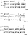
- FIGS. 3-14 illustrate a schematic cross-sectional view corresponding to a step of an exemplary method for fabricating an exemplary semiconductor structure consistent with disclosed embodiments.
- the method for fabricating the semiconductor structure may include providing a base 100.
- the base 100 may include a first region 100nl and a second region 100ns for forming transistors.
- the work function layer for the transistor formed by the second region 100ns of the base 100 may have a thickness greater than the work function layer for the transistor formed by the first region 100nl of the base 100.
- the base 100 may be used to provide a process operation platform.
- the material of the base 100 may include single crystal silicon.
- the material of the base may be selected from polycrystalline silicon or amorphous silicon.
- the material of the base may also be selected from germanium, gallium arsenide, silicon germanium compounds, or other suitable semiconductor materials.
- the base may include a silicon structure having an epitaxial layer or on an epitaxial layer.
- the semiconductor structure may include a planar transistor, and accordingly, the base 100 may be a planar base.
- the semiconductor structure may include a fin field effect transistor, and accordingly, the base may include a substrate and discrete fins on the substrate.
- the first region 100nl of the base 100 and the second region 100ns of the base 100 may be used to form N-type transistors, and the N-type transistor formed by the first region 100n1 of the base 100 may have a threshold voltage lower than the N-type transistor formed by the second region 100ns of the base 100.
- the N-type transistor formed by the first region 100nl of the base 100 may have a work function layer thinner than the N-type transistor formed by the second region 100ns of the base 100.
- the base 100 may further include a third region lOOps and a fourth region 100pl.
- the work function layer for the transistor formed by the third region 100ps of the base 100 may have a thickness greater than the work function layer for the transistor formed by the second region 100ns of the base 100.
- the work function layer for the transistor formed by the fourth region 100pl of the base 100 may have a thickness greater than the work function layer for the transistor formed by the third region lOOps of the base 100.
- the third region lOOps of the base 100 and the fourth region 100pl of the base 100 may be used to form P-type transistors.
- the P-type transistor formed by the third region 100ps of the base 100 may have a threshold voltage greater than the P-type transistor formed by the forth region 100pl of the base 100.
- the work function layer for the P-type transistor formed by the fourth region 100pl of the base 100 may have a thickness greater than the work function layer of the P-type transistor formed by the third region 100ps of the base 100.
- the work function layer for the P-type transistor formed by the third region lOOps of the base 100 may have a thickness greater than the work function layer for the N-type transistor formed by the second region 100ns of the base 100.
- the work function layer for the N-type transistor formed by the second region 100ns of the base 100 may have a thickness greater than the work function layer for the N-type transistor formed by the first region 100nl of the base 100.
- the method for fabricating the semiconductor structure may further include forming a gate dielectric layer 110 on the base 100.
- the base 100 may further include a third region lOOps and a fourth region 100pl.
- the gate dielectric layer 110 when forming the gate dielectric layer 110, the gate dielectric layer 110 may also be located on the third region lOOps of the base 100, and the gate dielectric layer 110 may also be located on the fourth region 100pl of the base 100.
- the semiconductor structure may have a "high-K metal gate” structure. Accordingly, the exemplary step of forming the gate dielectric layer 110 on the base 100 thus may include: forming the gate dielectric layer 110 having a high-K dielectric layer.
- the material of the high-k dielectric layer may include a gate dielectric material having a relative dielectric constant greater than the relative dielectric constant of silicon oxide.
- the material of the high-k dielectric layer may include hafnium oxide.
- the material of the high-K dielectric layer may include one or more materials selected from zirconium oxide, lanthanum oxide, aluminum oxide, titanium oxide, strontium titanate, lanthanum aluminum oxide, yttrium oxide, hafnium oxynitride, zirconium oxynitride, lanthanum oxynitride, aluminum oxynitride, titanium oxynitride, strontium titanium oxynitride, lanthanum aluminum oxynitride, and yttrium oxynitride.
- the method of forming the gate dielectric layer 110 may be a chemical vapor deposition, a physical vapor deposition, an atomic layer deposition, or other suitable film deposition.
- the method for fabricating the semiconductor structure may further include: forming an interface layer (IL) (not shown in FIG. 3 ) on the base 100, to solve the lattice mismatch issue between the base 100 and the gate dielectric layer 110.
- IL interface layer
- the method for fabricating the semiconductor structure may further include: forming a first material layer 121 on the gate dielectric layer 110.
- the first material layer 121 may be used to form a work function layer for the transistor formed by the first region 100nl of the base 100; and may also be used to form a work function layer for the transistor formed by the second region 100ns of the base 100.
- the base 100 may further include a third region lOOps and a fourth region 100pl. Accordingly, the first material layer 121 may also be used to form a work function layer for the transistor formed by the third region lOOps of the base 100, and a work function layer for the transistor formed by the fourth region 100pl of the base 100.
- the first material layer 121 when forming the first material layer 121, the first material layer 121 may also be located above the third region lOOps of the base 100, and the first material layer 121 may also be located above the fourth region 100pl of the base 100.
- the first region 100nl of the base 100 and the second region 100ns of the base 100 may be used to form N-type transistors.
- the first material layer 121 may include a layer of titanium nitride or stacked layers of titanium nitride and tantalum nitride, which may be formed by a chemical vapor deposition, a physical vapor deposition, an atomic layer deposition, or other suitable film deposition process.
- the method for fabricating the semiconductor structure may further include: forming an etch stop layer 130 on the first material layer 121.
- the etch stop layer 130 may be used to protect the first material layer 121 and the gate dielectric layer 110 in a subsequent semiconductor process, thereby reducing the possibility of damage to the first material layer 121 and the gate dielectric layer 110, enlarging the process window of the subsequent semiconductor process, and reducing the process difficulty of fabricating the semiconductor structure.
- the material of the etch stop layer 130 may be different from the material of the first material layer 121, thereby effectively stopping the etch process in the subsequent process and reducing the probability of damage to the first material layer 121 and the gate dielectric layer 110.
- the material of the etch stop layer 130 may include amorphous silicon, silicon nitride, or silicon oxide.
- the etch stop layer 130 may include an amorphous silicon layer.
- the exemplary step of forming the etch stop layer 130 may include: forming an amorphous silicon cap layer on the first material layer 121; and carrying out a post cap annealing (PCA).
- PCA post cap annealing
- the amorphous silicon cap layer on the first material layer 121 may serve as the etch stop layer 130.
- the etch stop layer 130 may be formed without adding an additional process, by using the amorphous silicon cap layer formed prior to the post cap annealing treatment as the etch stop layer 130. Accordingly, the simplification of the process steps may be facilitated, the process difficulty may be reduced, and the process cost may be reduced.
- the etch stop layer 130 may have a thickness in the range of approximately 20 angstroms to 80 angstroms when forming the etch stop layer 130.
- the base 100 may include a first region 100nl and a second region 100ns. Accordingly, the etch stop layer 130 may be located on the first material layer 121 above the first region 100nl of the base 100 and above the second region 100ns of the base 100.
- the base 100 may further include a third region lOOps and a fourth region 100pl.
- the etch stop layer 130 may also be located above the third region lOOps of the base 100, and the etch stop layer 130 may also be located above the fourth region 100pl of the base 100.
- the method for fabricating the semiconductor structure may further include: removing the etch stop layer 130 above the second region 100ns (as shown in FIG. 11 ) to expose the first material layer 121 above the second region 100ns.
- the step of removing the etch stop layer 130 above the second region 100ns may be used to expose the first material layer 121 above the second region 100ns, providing an operation surface for the subsequent process.
- the base 100 may further include a third region 100ps.
- the method for fabricating the semiconductor structure may further include: after forming the etch stop layer 130 on the first material layer 121, before removing the etch stop layer 130 above the second region 100ns, forming a third material layer 123 on the etch stop layer 130 and on the first material layer 121 above the third region lOOps.
- the third material layer 123 may be used to form the work function layer for the transistor formed by the third region 100ps of the base 100.
- the method for fabricating the semiconductor structure may further include: after forming the etch stop layer 130, before forming a third material layer 123, removing the etch stop layer 130 above the third region lOOps to expose the first material layer 121 above the third region lOOps.
- the base 100 may further include a fourth region 100pl.
- the method for fabricating the semiconductor structure may further include: after forming the etch stop layer 130 on the first material layer 121, before forming the third material layer 123 on the etch stop layer 130 and on the first material layer 121 above the third region 100ps, forming a fourth material layer 124 on the etch stop layer 130 and on the first material layer 121 above the fourth region 100pl.
- the fourth material layer 124 may be used to form the work function layer for the transistor formed by the fourth region 100pl of the base 100.
- the etch stop layer 130 may also be located above the fourth region 100pl of the base 100.
- the method for fabricating the semiconductor structure may further include: removing the etch stop layer 130 above the fourth region 100pl of the base 100 to expose the first material layer 121 above the fourth region 100pl.
- the removing of the etch stop layer 130 above the fourth region 100pl of the base 100 may be used to expose the first material layer 121 above the fourth region 100pl, such that the formed fourth material layer 124 may cover the surface of the first material layer 121.
- the removing of the stopping layer 130 above the fourth gate dielectric layer 110pl may include: forming a first pattern layer (not shown) on the etch stop layer 130, where the pattern layer may expose the etch stop layer 130 above the fourth region 100pl; and removing the etch stop layer 130 above the fourth region 100pl with the first pattern layer as a mask.
- the fourth gate dielectric layer 110pl may refer to the gate dielectric layer above the fourth region 100pl.
- the first pattern layer may be used to pattern the etch stop layer 130 to protect the etch stop layer 130 above the first region 100nl, the second region 100ns, and the third region 100ps.
- the first pattern layer may include a photoresist layer and may be formed by a coating process and a photolithography process.
- the first pattern layer may also be formed by a multiple patterning process (i.e. multiple patterning mask process).
- the multiple patterning process may include: a self-aligned double patterning (SaDP) process, a self-aligned triple patterning process, or a self-aligned quadruple patterning (i.e. Self-aligned Double Double Patterning, SaDDP) process.
- the exemplary step of removing the etch stop layer 130 above the fourth region 100pl may include: removing the etch stop layer 130 above the fourth region 100pl by wet etching.
- wet etching to remove the etch stop layer 130, the damage caused by the process of removing the etch stop layer 130 to the gate dielectric layer 110 and the first material layer 121 above the fourth region 100pl may be effectively reduced. Accordingly, the quality of the formed transistor may be improved, and the performance of the semiconductor structure may be improved.
- the etch stop layer 130 may include an amorphous silicon layer.
- the exemplary step of removing the etch stop layer 130 by wet etching may include: etching with an alkaline etching solution to remove the etch stop layer 130.
- the alkaline etching solution may include tetramethylammonium hydroxide (TMAH) solution or aqueous ammonia (NH 4 OH).
- TMAH tetramethylammonium hydroxide
- TMAH tetramethylammonium hydroxide
- the etching rate for the etch stop layer 130 may be substantially different from the etching rate for the first material layer 121. Accordingly, the possibility of damage to the first material layer 121 caused by the etching process may be effectively reduced, etching process window may be enlarged, and the performance of the corresponding semiconductor structure may be improved.
- TMAH tetramethylammonium hydroxide
- the etch stop layer above the fourth region may be removed by dry etching when removing the etch stop layer above the fourth region 100pl.
- the dry etching may be a soft dry etching.
- the dry etching process may be carried out by adopting a fluorine-containing plasma.
- the fluorine-containing plasma may include CF 4 , SF 6 or other fluorine-based plasma.
- the method for fabricating the semiconductor structure may further include: forming a fourth material layer 124 on the etch stop layer 130 and on the first material layer 121 above the fourth region 100pl.
- the transistor formed by the fourth region 100pl of the base 100 may be a P-type transistor.
- the material of the fourth material layer 124 may include titanium nitride, and may be formed by chemical vapor deposition, physical vapor deposition, atomic layer deposition, or other suitable film deposition process.
- the method for fabricating the semiconductor structure may further include: after forming the fourth material layer 124, as shown in FIGS. 7-8 , removing the etch stop layer 130 above the third region lOOps to expose the first material layer 121 above the third region lOOps.
- the exemplary step of removing the etch stop layer 130 above the third region lOOps to expose the first material layer 121 above the third region lOOps may include: removing the fourth material layer 124 on the etch stop layer 130 above the third region lOOps, to expose the etch stop layer 130 above the third region lOOps.
- the exemplary step of removing the fourth material layer 124 on the etch stop layer 130 above the third region lOOps may include: forming a second pattern layer on the fourth material layer 124, where the second pattern layer may expose the fourth material layer 124 on the etch stop layer 130 above the third region lOOps; and removing the fourth material layer 124 on the etch stop layer 130 above the third region lOOps, with the second pattern layer as a mask, to expose the etch stop layer 130 above the third region lOOps.
- the second pattern layer may be used to protect the etch stop layer 130 above the first region 100nl and the second region 100ns, and also to protect the fourth material layer 124 above the fourth region 100pl.
- the second pattern layer may include a photoresist layer, which may be formed by a coating process and a photolithography process. In other embodiments, the second pattern layer may also be formed by a multiple patterning process.
- the exemplary step of removing the fourth material layer 124 above the third region 100ps may be used to expose the etch stop layer 130 above the third region 100ps, providing a process surface for removing the etch stop layer 130.
- the exemplary step of removing the fourth material layer 124 above the third region lOOps may include: removing the fourth material layer 124 above the third region lOOps by wet etching.
- the material of the fourth material layer 124 may include titanium nitride
- the etching solution may include a mixed solution of NH 4 OH, H 2 O 2 and water (SC1 solution), a mixed solution of NH 4 , H 2 O 2 and water, or a mixed solution of HCl, H 2 O 2 and water (SC2 solution).
- the etch stop layer 130 may be provided above the third region 100ps, the etch stop layer 130 may effectively reduce the possibility of damage to the gate dielectric layer 110 and the first material layer 121 above the third region lOOps, during the wet etching to remove the fourth material layer 124. Accordingly, the quality of the formed transistor may be improved, and the performance of the fabricated semiconductor structure may be improved.
- the method for fabricating the semiconductor structure may further include: removing the etch stop layer 130 above the third region lOOps to expose the first material layer 121 above the third region lOOps.
- the exemplary step of removing the etch stop layer 130 above the third region lOOps may be used to expose the first material layer 121 above the third region 100ps, thereby providing an operation surface for subsequent processes.
- the exemplary step of removing the etch stop layer 130 above the third region lOOps may include: removing the etch stop layer 130 by wet etching or dry etching, which may be the same or similar etching process as for removing the etch stop layer 130 above the fourth region 100pl as previously described.
- any suitable methods may be used to remove a portion of the etch stop layer 130.
- the method for fabricating the semiconductor structure may further include: forming a third material layer 123 above the etch stop layer 130, and on the first material layer 121 above the third region lOOps.
- the third material layer 123 may be used to form a work function layer for the transistor formed by the third region 100ps of the base 100.
- the transistor formed by the third region 100ps of the base 100 may be a P-type transistor.
- the material of the third material layer 123 may include titanium nitride, and may be formed by chemical vapor deposition, physical vapor deposition, atomic layer deposition or other suitable film deposition process.
- the base 100 may further include a fourth region 100pl.
- the third material layer 123 when forming the third material layer 123 above the etch stop layer 130, and on the first material layer 121 above the third region lOOps, the third material layer 123 may also be located on the fourth material layer 124 above the fourth region 100pl.
- the fourth material layer 124 may also be located on the etch stop layer 130 above the first region 100nl and the second region 100ns.
- the third material layer 123 may also be located on the fourth material layer 124. That is, the third material layer 123 may also be located on the fourth material layer 124 on the etch stop layer 130 above the first region 100nl and the second region 100ns.
- the method for fabricating the semiconductor structure may further include: after forming the third material layer 123, as shown in FIGS. 10-11 , removing the etch stop layer 130 above the second region 100ns to expose the first material layer 121 above the second region 100ns.
- the step of removing the etch stop layer 130 above the second region 110ns may include: removing the fourth material layer 124 and the third material layer 123 above the second region 110ns, to expose the etch stop layer 130 above the second region 110ns.
- the exemplary step of removing the fourth material layer 124 and the third material layer 123 above the second region 110ns may include: forming a third pattern layer on the third material layer 123, where the third pattern layer may expose the third material layer 123 above the etch stop layer 130 above the second region 100ns; and removing the fourth material layer 124 and the third material layer 123 above the etch stop layer 130 above the second region 100ns, with the third pattern layer as a mask, until the etch stop layer 130 above the second region 100ns is exposed.
- the third pattern layer may be used to protect the etch stop layer 130 above the first region 100nl, also to protect the third material layer 123 above the third region lOOps, and to protect the third material layer 123 and the fourth material layer 124 above the fourth region 100pl.
- the third pattern layer may include a photoresist layer, and may be formed by a coating process and a photolithography process. In other embodiments, the third pattern layer may also be formed by a multiple patterning process.
- the exemplary step of removing the fourth material layer 124 and the third material layer 123 above the etch stop layer 130 above the second region 100ns may be used to expose the etch stop layer 130 above the second region 100ns, thereby providing a process surface for removing the etch stop layer 130.
- the exemplary step of removing the fourth material layer 124 and the third material layer 123 above the etch stop layer 130 above the second region 100ns may include: removing the fourth material layer 124 and the third material layer 123 above the second region 110ns by wet etching.
- the third material layer 123 and the fourth material layer 124 may both include titanium nitride.
- the removal of one or both of the third material layer 123 and the fourth material layer 124 may refer to the above-described process for etching the fourth material layer 124.
- any suitable methods may be used to remove the third material layer 123 and/or the fourth material layer 124.
- the method for fabricating the semiconductor structure may further include: after exposing the etch stop layer 130 above the second region 110ns, as shown in FIG. 11 , removing the etch stop layer 130 above the second region 110ns.
- the step of removing the etch stop layer 130 above the second region 110ns may be used to expose the first material layer 121 above the second region 100ns, thereby providing a process surface for the subsequent processes.
- the step of removing the etch stop layer 130 above the second region 110ns may include: removing the etch stop layer 130 by wet etching or dry etching, which may be the same or similar etching process as for removing the etch stop layer 130 above the fourth region 100pl as previously described.
- any suitable methods may be used to remove a portion of the etch stop layer 130.
- the method for fabricating the semiconductor structure may further include: forming a second material layer 122 above the etch stop layer 130, and on the first material layer 121 above the second region 100ns.
- the second material layer 122 and the first material layer 121 above the second region 100ns may be used to form the work function layer for the transistor formed by the second region 100ns of the base 100.
- the second material layer 122 may be used to form the work function layer for the transistor formed by the second region 100ns of the base 100.
- the second region 100ns of the base 100 may be used to form an N-type transistor.
- the material of the second material layer 122 may include titanium nitride, and may be formed by chemical vapor deposition, physical vapor deposition, atomic layer deposition, or other suitable film deposition process.
- the base 100 may also include a third region lOOps and a fourth region 100pl.
- the second material layer 122 may also be located on the third material layer 123.
- the second material layer 122 may be located on the third material layer 123 above the third region lOOps and the fourth region 100pl.
- the second material layer 122 and the first material layer 121 above the second region 100ns may be used to form a work function layer for the transistor formed by the second region 100ns of the base 100.
- the second material layer 122, the third material layer 123, and the first material layer 121 above the third region lOOps may be used to form the work function layer for the transistor formed by the third region lOOps of the base 100.
- the transistor formed by the third region 100ps of the base 100 may have a work function layer thicker than the transistor formed by the second region 100ns of the base 100.
- the third material layer 123 above the fourth region 100pl may be further located on the fourth material layer 124 above the fourth region 100pl.
- the second material layer 122, the third material layer 123, the fourth material layer 124, and the first material layer 121 above the fourth region 100pl may be used to form a work function layer for the transistor formed by the fourth region 100pl of the base 100.
- the transistor formed by the fourth region 100pl of the base 100 may have a work function layer thicker than the transistor formed by the third region lOOps of the base 100.
- the method for fabricating the semiconductor structure may further include: removing the second material layer 122 above the first region 100nl, with the etch stop layer 130 as a stopping layer, to expose the first material layer 121 above the first region 100nl.
- the first material layer 121 above the first region 100nl may be used to form the work function layer for the transistor formed by the first region 100nl of the base 100.
- the step of exposing the first material layer 121 by removing the second material layer 122 above the first region 100nl with the etch stop layer 130 as a stopping layer may include: as shown in FIG. 13 , removing the second material layer 122 above the first region 100nl, with the etching stopping layer 130 as a stopping layer, to expose the etch stop layer 130 above the first region 100nl; and, as shown in FIG. 14 , removing the etch stop layer 130 above the first region 100nl, to expose the first material layer 121 above the first region 100nl.
- a third material layer 123 may be provided above the etch stop layer 130 above the first region 100nl.
- the step of exposing the first material layer 121, by removing the second material layer 122 above the first region 100nl with the etch stop layer 130 as a stopping layer may include: exposing the etch stop layer 130, by removing the second material layer 122 and the third material layer 123 above the first region 100nl, with the etch stop layer 130 as a stopping layer; and exposing the first material layer 121 by removing the etch stop layer 130.
- a fourth material layer 124 may be provided on the etch stop layer 130 above the first region 100nl. That is, a fourth material layer 124, a third material layer 123, and a second material layer 122 may be provided above the etch stop layer 130 above the first region 100nl.
- the step of exposing the first material layer 121, by removing the second material layer 122 above the first region 100nl with the etch stop layer 130 as a stopping layer may include: exposing the etch stop layer 130, by removing the second material layer 122, the third material layer 123, and the fourth material layer 124 above the first region 100nl with the etch stop layer 130 as a stopping layer; and exposing the first material layer 121 by removing the etch stop layer 130.
- the step of removing the fourth material layer 124, the third material layer 123, and the second material layer 122 above the first region 100nl may include: forming a fourth pattern layer on the second material layer 122, where the fourth pattern layer may expose the second material layer 122 above the first region 100nl; and removing the fourth material layer 124, the third material layer 123, and the second material layer 122 above the first region 100nl, with the fourth pattern layer as a mask, until the etch stop layer 130 above the first region 100nl is exposed.
- the fourth pattern layer may be used to protect the second material layer 122, the third material layer 123, and the fourth material layer 124 above the fourth region 100pl; also to protect the second material layer 122 and the third material layer 123 above the third region 100ps; and to protect the second material layer 122 above the second region lOOps.
- the fourth pattern layer may include a photoresist layer, and may be formed by a coating process and a photolithography process. In other embodiments, the fourth pattern layer may also be formed by a multiple patterning process.
- the step of removing the fourth material layer 124, the third material layer 123, and the second material layer 122 above the first region 100nl may be used to expose the etch stop layer 130, providing a process surface for removing the etch stop layer 130.
- the step of removing the fourth material layer 124, the third material layer 123, and the second material layer 122 above the first region 100nl may include: removing the fourth material layer 124, the third material layer 123, and the second material layer 122 above the first region 100nl by wet etching.
- the second material layer 122, the third material layer 123 and the fourth material layer 124 each may include titanium nitride.
- the removal of one or more of the second material layer 122, the third material layer 123 and the fourth material layer 124 may refer to the above-described process for etching the fourth material layer 124.
- any suitable methods may be used to remove the second material layer 122, the third material layer 123 and/or the fourth material layer 124.
- the step of removing the etch stop layer 130 above the first region 100nl may be used to expose the first material layer 121 above the first region 100nl.
- the step of removing the etch stop layer 130 above the first region 100nl may include: removing the etch stop layer 130 by wet etching or dry etching, which may be the same or similar etching process as for removing the etch stop layer 130 above the fourth region 100pl as previously described.
- any suitable methods may be used to remove a portion of the etch stop layer 130.
- the N-type transistor formed by the second region 100ns of the base 100 may have a work function layer thicker than the N-type transistor formed by the first region 100nl of the base 100; the P-type transistor formed by the third region lOOps of the base 100 may have a work function layer thicker than the N-type transistor formed by the second region 100ns of the base 100; and the P-type transistor formed by the fourth region 100pl of the base 100 may have a work function layer thicker than the P-type transistor formed by the third region lOOps of the base 100.
- the thickness of the first material layer 121 may be determined according to the thickness of the work function layer for the N-type transistor formed by the first region 100nl of the base 100.
- the thickness of the second material layer 122 may be determined according to the thickness of the work function layer for the N-type transistor formed by the second region 100ns of the base 100 and the thickness of the first material layer 121.
- the thickness of the third material layer 123 may be determined according to the thickness of the work function layer for the P-type transistor formed by the third region lOOps of the base 100, the thickness of the first material layer 121, and the thickness of the second material layer 122.
- the thickness of the fourth material layer 124 may be determined according to the thickness of the work function layer for the P-type transistor formed by the fourth region 100pl of the base 100, the thickness of the first material layer 121, the thickness of the second material layer 122, and the thickness of the third material layer 123.
- the base 100 may include a first region 100nl, a second region 100ns, a third region lOOps, and a fourth region 100pl, forming the transistors having work function layers with a successively increased thickness, which is merely for illustrative purposes.
- the base 100 may include any two regions selected from of the first region 100nl, the second region 100ns, the third region 100ps, and the fourth region 100pl.
- first region 100nl, the second region 100ns, the third region lOOps, and the fourth region 100pl may be isolated from each other.
- first region, the second region, the third region, and the fourth region may also be adjacent regions.
- any number of the first regions, the second regions, the third regions, or the fourth regions may be included for the disclosed semiconductor structure, more regions, e.g., a fifth region, a sixth region, etc. may also be added.
- an etch stop layer may be formed on the first material layer after the formation of the first material layer; and the second material layer above the first region may be removed with the etch stop layer as an etch stopping layer.
- the process window for the step of removing the second material layer above the first region may be effectively enlarged by adding the etch stop layer, thereby effectively reducing the process control difficulty of removing the second material layer above the first region. Accordingly, the accuracy of the thickness control of the work function layer in the semiconductor structure may be improved, and the performance of the semiconductor structure may be improved.
- the gate dielectric layer may be protected by the etching stop layer, facilitating the reduction of the thickness of the first material layer, and facilitating the adjustment of the threshold voltage of the corresponding transistor.
- the etch stop layer may be an amorphous silicon cap layer formed in a post cap annealing process.
- the formation of the etch stop layer may not require an additional process step.
- the etch stop layer may be removed by wet etching. No additional process risk may be introduced for the fabrication of the semiconductor structure, facilitating the improvement on the performance of the semiconductor structure without increasing the process steps and the process cost.
- the etch stop layer may also protect the first material layer and the gate dielectric layer during the process, and reduce damage to the gate dielectric layer and the first material layer, facilitating the improvement on the performance of the fabricated semiconductor structure.
- the present invention provides a method for fabricating a semiconductor structure.
- the method may include: providing a base including a first region and a second region; forming a gate dielectric layer and a first material layer; forming an etch stop layer; removing the etch stop layer above the second region; forming a second material layer; and exposing the first material layer above the first region with the etch stop layer as a stopping layer.
- the process window of the step for removing the second material layer above the first region may be effectively enlarged by adding the etch stop layer, thereby effectively reducing the process control difficulty of removing the second material layer above the first region. Accordingly, the accuracy of the thickness control of the work function layer in the semiconductor structure may be improved, and the performance of the semiconductor structure may be improved.
- the gate dielectric layer may be protected by the etch stop layer, thereby facilitating the reduction of the thickness of the first material layer, and facilitating the adjustment of the threshold voltage of the corresponding transistor.
- the present invention provides the technical solution having the following advantages.
- an etch stop layer may be formed on the first material layer after the formation of the first material layer; and the second material layer above the first region may be removed with the etch stop layer as a stopping layer.
- the process window of the step for removing the second material layer above the first region may be effectively enlarged by adding the etch stop layer, thereby effectively reducing the process control difficulty of removing the second material layer above the first region. Accordingly, the accuracy of the thickness control of the work function layer in the semiconductor structure may be improved, and the performance of the semiconductor structure may be improved.
- the gate dielectric layer may be protected by the etch stop layer, facilitating the reduction of the thickness of the first material layer, and facilitating the adjustment of the threshold voltage of the corresponding transistor.
- the etch stop layer may be an amorphous silicon cap layer formed in a post cap annealing process.
- the formation of the etch stop layer may not require an additional process step.
- the etch stop layer may be removed by wet etching. No additional process risk may be introduced for the fabrication of the semiconductor structure, facilitating the improvement on the performance of the semiconductor structure without increasing the process steps and the process cost.
- the etch stop layer may also protect the first material layer and the gate dielectric layer during the process, and reduce damage to the gate dielectric layer and the first material layer, facilitating the improvement on the performance of the fabricated semiconductor structure.
Landscapes
- Chemical & Material Sciences (AREA)
- Chemical Kinetics & Catalysis (AREA)
- General Chemical & Material Sciences (AREA)
- Metal-Oxide And Bipolar Metal-Oxide Semiconductor Integrated Circuits (AREA)
- Engineering & Computer Science (AREA)
- Manufacturing & Machinery (AREA)
- Thin Film Transistor (AREA)
Abstract
Description
- This application claims priority of Chinese Patent Application No.
201611089134.0, filed on November 30, 2016 - The present invention generally relates to the field of semiconductor manufacturing technologies and, more particularly, relates to semiconductor structures and fabrication method thereof.
- With rapid development of semiconductor manufacturing technology, semiconductor devices develop toward higher element density, and higher integration level. Transistors are currently widely used as the most basic semiconductor devices. With increasing element density and integration level of the semiconductor devices, the characteristic sizes of the transistors are getting smaller and smaller. In order to reduce the parasitic capacitance of the transistor gate and improve device speed, gate structures having a high-K gate dielectric layer and a metal gate electrode are introduced into the transistor.
- However, problems remain when forming a metal gate electrode on a high-K gate dielectric layer, due to a matching problem of the work function. The work function will directly influence the threshold voltage (Vt) of the device and the performance of the transistor. Thus, a work function layer is introduced into the high-K metal gate structure to adjust threshold voltage of the resultant device.
- However, even if a work function layer is introduced in the high-K metal gate structure, the performance of the semiconductor structure in the existing technology still needs to be improved.
- It is an object of the present invention to provide a semiconductor structure and a method for fabricating the same which may solve one or more problems in the prior art as such discussed above, in particular which may improve the performance of the semiconductor structure even if a work function layer is introduced in the high-K metal gate structure.
- The object is achieved by the features of the respective independent claims. Further embodiments and developments are defined in the dependent claims.
- A first aspect of the present invention provides a method for fabricating a semiconductor structure by providing a base including a first region, a second region, a third region, and a fourth region for forming a first transistor, a second transistor, a third transistor, and a fourth transistor, respectively. A gate dielectric layer is formed on the first, second, third and fourth regions of the base. A first material layer is formed on the gate dielectric layer. An etch stop layer is formed on the first material layer. The etch stop layer above the fourth region is removed. A second material layer is formed on the remaining etch stop layer and on the first material layer above the fourth region. The second material layer and the etch stop layer above the third region are removed to expose the first material layer above the third region. A third material layer is formed on the remaining second material layer above the first, second and further regions, and on the exposed first material layer above the third region. The etch stop layer, and the second and third material layers above the second region are removed to expose the first material layer above the second region. A fourth material layer is formed on the remaining third material layer above the first, second and further regions, and on the exposed first material layer above the third region. The etch stop layer and the second, third, and fourth material layers above the first region are removed to expose the first material layer above the first region.
- Preferably, the first material layer above the first region is used as a first work function layer for the first transistor.
- Preferably, the first and fourth material layers above the second region are used as a second work function layer for the second transistor.
- Preferably, the first, third and fourth material layers above the third region are used as a third work function layer for the third transistor.
- Preferably, the first, second, third and fourth material layers above the fourth region are used as a fourth work function layer for the fourth transistor.
- Preferably, the etch stop layer is made of a material including an amorphous silicon, a silicon nitride, a silicon oxide, or a combination thereof.
- Preferably, the etch stop layer is made of the amorphous silicon, and is formed by a process comprising: forming an amorphous silicon cap layer on the first material layer; and performing a post cap annealing to form the amorphous silicon cap layer on the first material layer as the etch stop layer.
- Preferably, the etch stop layer has a thickness in a range of approximately 20 Å to 80 Å.
- Preferably, the etch stop layer is removed by a wet etching or a dry etching.
- Preferably, the etch stop layer is etched by an alkaline etching solution including a tetramethylammonium hydroxide solution or an ammonia.
- Preferably, the etch stop layer is etched by a fluorine-based plasma, the fluorine-based plasma including CF4 or SF6.
- Preferably, the first and second transistors formed in the first and second regions of the base include N-type transistors. Preferably, the N-type transistor in the first region of the base has a threshold voltage smaller than the N-type transistor formed in the second region of the base.
- Preferably, the third and fourth transistors formed in the third and fourth regions of the base include P-type transistors.
- Preferably, the P-type transistor in the third region of the base has a threshold voltage greater than the P-type transistor formed in the fourth region of the base.
- Preferably, one or both of the first and second material layers include a titanium nitride layer or a stacked layer including a titanium nitride layer and a tantalum nitride layer.
- Preferably, one or both of the third and fourth material layers are made of a material including titanium nitride.
- A second aspect of the present invention provides a semiconductor structure. The semiconductor structure includes a base including a first region, a second region, a third region, and a fourth region, used for a first transistor, a second transistor, a third transistor, and a fourth transistor, respectively. A gate dielectric layer is on the first, second, third and fourth regions of the base. A first material layer is on the gate dielectric layer. A second material layer is on the first material layer above the fourth region. A third material layer is on the first material layer above the third region and on the second material layer above the fourth region. A fourth material layer is on the third material layer above the third and fourth regions and on the first material layer on the second region. The first material layer above the first region is used as a first work function layer for the first transistor. The first and fourth material layers above the second region are used as a second work function layer for the second transistor. The first, third and fourth material layers above the third region are used as a third work function layer for the third transistor. The first, second, third and fourth material layers above the fourth region are used as a fourth work function layer for the fourth transistor.
- Preferably, the first and second transistors formed in the first and second regions of the base include N-type transistors.
- Preferably, the N-type transistor in the first region of the base has a threshold voltage smaller than the N-type transistor formed in the second region of the base.
- Preferably, the third and fourth transistors formed in the third and fourth regions of the base include P-type transistors.
- Preferably, the P-type transistor in the third region of the base has a threshold voltage greater than the P-type transistor formed in the fourth region of the base.
- Preferably, one or both of the first and second material layers include a titanium nitride layer or a stacked layer including a titanium nitride layer and a tantalum nitride layer.
- Preferably, one or both of the third and fourth material layers are made of a material including titanium nitride.
- A semiconductor structure according to the second aspect of the present invention may be obtained by a method according to the first aspect of the present invention.
- Other aspects of the present invention can be understood by those skilled in the art in light of the description, the claims, and the drawings of the present invention.
- The following drawings are merely examples for illustrative purposes according to various disclosed embodiments and are not intended to limit the present invention.
-
FIGS. 1-2 illustrate a schematic cross-sectional view corresponding to a method for forming a semiconductor structure; and -
FIGS. 3-14 illustrate a schematic cross-sectional view corresponding to each step of an exemplary method for fabricating an exemplary semiconductor structure consistent with disclosed embodiments. - The objects, features and advantages of the present invention can be understood by those skilled in the art through the exemplary embodiments of the present invention and further described in detail with reference to the accompanying drawings.
-
FIGS. 1-2 illustrate a schematic cross-sectional view corresponding to a method for forming a semiconductor structure. - As shown in
FIG. 1 , at the beginning of the fabrication process, a base is provided. The base may include afirst region 10a and asecond region 10b for forming N-type transistors. The work function layer for the transistor formed by thesecond region 10b of the base may have a thickness greater than the work function layer for the transistor formed by thefirst region 10a of the base. - As shown in
FIG. 1 , agate dielectric layer 11 is formed on thebase 10, and afirst material layer 12 is formed on thegate dielectric layer 11. Asecond material layer 13 is formed on thefirst material layer 12. - As shown in
FIG. 2 , thesecond material layer 13 above thefirst region 10a of thebase 10 is removed to expose thefirst material layer 12 above thefirst region 10a of thebase 10. - The
first material layer 12 above thefirst region 10a of the base 10 may be used for forming a work function layer for the N-type transistor formed by thefirst region 10a of thebase 10. Thefirst material layer 12 and thesecond material layer 13 above thesecond region 10b of the base 10 may be used for forming a work function layer for the N-type transistor formed by thesecond region 10b of thebase 10. In some cases, the material of thefirst material layer 12 may include titanium nitride or tantalum nitride, and the material of thesecond material layer 13 may include titanium nitride. - The difference between the etching rates of titanium nitride and tantalum nitride may not be sufficiently large when removing the
second material layer 13 above thefirst region 10a of thebase 10. Thus, the process control for removing thesecond material layer 13 above thefirst region 10a of the base 10 may be substantially difficult. Accordingly, accurately controlling the thicknesses of the work function layers of different devices in the fabricated semiconductor structure may be substantially difficult, thereby influencing the adjustment of the threshold voltages of the different devices in the semiconductor structure and the performance of the semiconductor structure. - A semiconductor structure may be formed by: providing a base having a first region and a second region for forming transistors, where the work function layer for the transistor formed by the second region of the base may have a thickness greater than the work function layer for the transistor formed by the first region of the base; forming a gate dielectric layer on the base; forming a first material layer on the gate dielectric layer; forming an etch stop layer on the first material layer; removing the etch stop layer above the second region to expose the first material layer above the second region; forming a second material layer on the etch stop layer and the first material layer above the second region, where the second material layer and the first material layer above the second region may be used for forming a work function layer for the transistor formed by the second region of the base; removing the second material layer above the first region with the etch stop layer as a stopping layer (e.g., to stop the etch process), to expose the first material layer above the first region, where the first material layer above the first region may be used for forming a work function layer for the transistor formed by the first region of the base.
- In the present invention, an etch stop layer may be formed on the first material layer after the formation of the first material layer; and the second material layer above the first region may be removed using the etch stop layer to stop the etch process. The process window for removing the second material layer above the first region may be effectively enlarged by adding the etch stop layer, thereby effectively reducing the process control difficulties for removing the second material layer above the first region. Accordingly, the accuracy of the thickness control of the work function layer in the semiconductor structure may be improved, and the performance of the semiconductor structure may be improved.
- In addition, by removing the second material layer above the first region with the etch stop layer to stop the etch process, the gate dielectric layer may be protected by the etch stop layer, thereby facilitating thickness reduction of the first material layer, and thereby facilitating the adjustment of the threshold voltage of the corresponding transistor.
-
FIGS. 3-14 illustrate a schematic cross-sectional view corresponding to a step of an exemplary method for fabricating an exemplary semiconductor structure consistent with disclosed embodiments. - As shown in
FIG. 3 , the method for fabricating the semiconductor structure may include providing abase 100. The base 100 may include a first region 100nl and a second region 100ns for forming transistors. The work function layer for the transistor formed by the second region 100ns of the base 100 may have a thickness greater than the work function layer for the transistor formed by the first region 100nl of thebase 100. - The base 100 may be used to provide a process operation platform.
- In various embodiments, the material of the base 100 may include single crystal silicon. In certain embodiments, the material of the base may be selected from polycrystalline silicon or amorphous silicon. In other embodiments, the material of the base may also be selected from germanium, gallium arsenide, silicon germanium compounds, or other suitable semiconductor materials. In some embodiments, the base may include a silicon structure having an epitaxial layer or on an epitaxial layer.
- In some embodiments, the semiconductor structure may include a planar transistor, and accordingly, the
base 100 may be a planar base. In other embodiments, the semiconductor structure may include a fin field effect transistor, and accordingly, the base may include a substrate and discrete fins on the substrate. - In various embodiments, the first region 100nl of the
base 100 and the second region 100ns of the base 100 may be used to form N-type transistors, and the N-type transistor formed by the first region 100n1 of the base 100 may have a threshold voltage lower than the N-type transistor formed by the second region 100ns of thebase 100. Thus, the N-type transistor formed by the first region 100nl of the base 100 may have a work function layer thinner than the N-type transistor formed by the second region 100ns of thebase 100. - In addition, the
base 100 may further include a third region lOOps and a fourth region 100pl. The work function layer for the transistor formed by the third region 100ps of the base 100 may have a thickness greater than the work function layer for the transistor formed by the second region 100ns of thebase 100. The work function layer for the transistor formed by the fourth region 100pl of the base 100 may have a thickness greater than the work function layer for the transistor formed by the third region lOOps of thebase 100. - For example, the third region lOOps of the
base 100 and the fourth region 100pl of the base 100 may be used to form P-type transistors. The P-type transistor formed by the third region 100ps of the base 100 may have a threshold voltage greater than the P-type transistor formed by the forth region 100pl of thebase 100. - Thus, the work function layer for the P-type transistor formed by the fourth region 100pl of the base 100 may have a thickness greater than the work function layer of the P-type transistor formed by the third region 100ps of the
base 100. The work function layer for the P-type transistor formed by the third region lOOps of the base 100 may have a thickness greater than the work function layer for the N-type transistor formed by the second region 100ns of thebase 100. The work function layer for the N-type transistor formed by the second region 100ns of the base 100 may have a thickness greater than the work function layer for the N-type transistor formed by the first region 100nl of thebase 100. - As shown in
FIG. 3 , the method for fabricating the semiconductor structure may further include forming agate dielectric layer 110 on thebase 100. - In various embodiments, the
base 100 may further include a third region lOOps and a fourth region 100pl. Thus, when forming thegate dielectric layer 110, thegate dielectric layer 110 may also be located on the third region lOOps of thebase 100, and thegate dielectric layer 110 may also be located on the fourth region 100pl of thebase 100. - In various embodiments, the semiconductor structure may have a "high-K metal gate" structure. Accordingly, the exemplary step of forming the
gate dielectric layer 110 on the base 100 thus may include: forming thegate dielectric layer 110 having a high-K dielectric layer. - The material of the high-k dielectric layer may include a gate dielectric material having a relative dielectric constant greater than the relative dielectric constant of silicon oxide. In various embodiments, the material of the high-k dielectric layer may include hafnium oxide. In other embodiments, the material of the high-K dielectric layer may include one or more materials selected from zirconium oxide, lanthanum oxide, aluminum oxide, titanium oxide, strontium titanate, lanthanum aluminum oxide, yttrium oxide, hafnium oxynitride, zirconium oxynitride, lanthanum oxynitride, aluminum oxynitride, titanium oxynitride, strontium titanium oxynitride, lanthanum aluminum oxynitride, and yttrium oxynitride.
- The method of forming the
gate dielectric layer 110 may be a chemical vapor deposition, a physical vapor deposition, an atomic layer deposition, or other suitable film deposition. - After providing the
base 100 and before forming thegate dielectric layer 110, the method for fabricating the semiconductor structure may further include: forming an interface layer (IL) (not shown inFIG. 3 ) on thebase 100, to solve the lattice mismatch issue between the base 100 and thegate dielectric layer 110. - As shown in
FIG. 4 , the method for fabricating the semiconductor structure may further include: forming afirst material layer 121 on thegate dielectric layer 110. - The
first material layer 121 may be used to form a work function layer for the transistor formed by the first region 100nl of thebase 100; and may also be used to form a work function layer for the transistor formed by the second region 100ns of thebase 100. - In various embodiments, the
base 100 may further include a third region lOOps and a fourth region 100pl. Accordingly, thefirst material layer 121 may also be used to form a work function layer for the transistor formed by the third region lOOps of thebase 100, and a work function layer for the transistor formed by the fourth region 100pl of thebase 100. - Thus, when forming the
first material layer 121, thefirst material layer 121 may also be located above the third region lOOps of thebase 100, and thefirst material layer 121 may also be located above the fourth region 100pl of thebase 100. - In various embodiments, the first region 100nl of the
base 100 and the second region 100ns of the base 100 may be used to form N-type transistors. Thus, when forming thefirst material layer 121, thefirst material layer 121 may include a layer of titanium nitride or stacked layers of titanium nitride and tantalum nitride, which may be formed by a chemical vapor deposition, a physical vapor deposition, an atomic layer deposition, or other suitable film deposition process. - As shown in
FIG. 4 , the method for fabricating the semiconductor structure may further include: forming anetch stop layer 130 on thefirst material layer 121. - The
etch stop layer 130 may be used to protect thefirst material layer 121 and thegate dielectric layer 110 in a subsequent semiconductor process, thereby reducing the possibility of damage to thefirst material layer 121 and thegate dielectric layer 110, enlarging the process window of the subsequent semiconductor process, and reducing the process difficulty of fabricating the semiconductor structure. - The material of the
etch stop layer 130 may be different from the material of thefirst material layer 121, thereby effectively stopping the etch process in the subsequent process and reducing the probability of damage to thefirst material layer 121 and thegate dielectric layer 110. For example, when forming theetch stop layer 130, the material of theetch stop layer 130 may include amorphous silicon, silicon nitride, or silicon oxide. - In various embodiments, the
etch stop layer 130 may include an amorphous silicon layer. For example, the exemplary step of forming theetch stop layer 130 may include: forming an amorphous silicon cap layer on thefirst material layer 121; and carrying out a post cap annealing (PCA). The amorphous silicon cap layer on thefirst material layer 121 may serve as theetch stop layer 130. - The
etch stop layer 130 may be formed without adding an additional process, by using the amorphous silicon cap layer formed prior to the post cap annealing treatment as theetch stop layer 130. Accordingly, the simplification of the process steps may be facilitated, the process difficulty may be reduced, and the process cost may be reduced. - It should be noted that, when the thickness of the
etch stop layer 130 is too small, the etch may not be effectively stopped in the subsequent process, and the protection on thefirst material layer 121 and thegate dielectric layer 110 may not be guaranteed. When the thickness of theetch stop layer 130 is too large, the material may be easily wasted, and the process difficulty may be increased. In various embodiments, theetch stop layer 130 may have a thickness in the range of approximately 20 angstroms to 80 angstroms when forming theetch stop layer 130. - For example, the
base 100 may include a first region 100nl and a second region 100ns. Accordingly, theetch stop layer 130 may be located on thefirst material layer 121 above the first region 100nl of thebase 100 and above the second region 100ns of thebase 100. - In various embodiments, the
base 100 may further include a third region lOOps and a fourth region 100pl. Thus, when forming anetch stop layer 130, theetch stop layer 130 may also be located above the third region lOOps of thebase 100, and theetch stop layer 130 may also be located above the fourth region 100pl of thebase 100. - Referring to
FIGS. 5-11 , the method for fabricating the semiconductor structure may further include: removing theetch stop layer 130 above the second region 100ns (as shown inFIG. 11 ) to expose thefirst material layer 121 above the second region 100ns. - The step of removing the
etch stop layer 130 above the second region 100ns may be used to expose thefirst material layer 121 above the second region 100ns, providing an operation surface for the subsequent process. - In various embodiments, the
base 100 may further include a third region 100ps. Thus, as shown inFIGS. 5-9 , the method for fabricating the semiconductor structure may further include: after forming theetch stop layer 130 on thefirst material layer 121, before removing theetch stop layer 130 above the second region 100ns, forming athird material layer 123 on theetch stop layer 130 and on thefirst material layer 121 above the third region lOOps. - The
third material layer 123 may be used to form the work function layer for the transistor formed by the third region 100ps of thebase 100. - Because the
etch stop layer 130 may also be located on the third region lOOps of thebase 100, as shown inFIGS. 6-8 , the method for fabricating the semiconductor structure may further include: after forming theetch stop layer 130, before forming athird material layer 123, removing theetch stop layer 130 above the third region lOOps to expose thefirst material layer 121 above the third region lOOps. - In addition, the
base 100 may further include a fourth region 100pl. Thus, as shown inFIGS. 5-6 , the method for fabricating the semiconductor structure may further include: after forming theetch stop layer 130 on thefirst material layer 121, before forming thethird material layer 123 on theetch stop layer 130 and on thefirst material layer 121 above the third region 100ps, forming afourth material layer 124 on theetch stop layer 130 and on thefirst material layer 121 above the fourth region 100pl. - The
fourth material layer 124 may be used to form the work function layer for the transistor formed by the fourth region 100pl of thebase 100. - It should be noted that, the
etch stop layer 130 may also be located above the fourth region 100pl of thebase 100. Thus, as shown inFIG. 5 , after forming theetch stop layer 130, before forming thefourth material layer 124, the method for fabricating the semiconductor structure may further include: removing theetch stop layer 130 above the fourth region 100pl of the base 100 to expose thefirst material layer 121 above the fourth region 100pl. - The removing of the
etch stop layer 130 above the fourth region 100pl of the base 100 may be used to expose thefirst material layer 121 above the fourth region 100pl, such that the formedfourth material layer 124 may cover the surface of thefirst material layer 121. - In various embodiments, the removing of the stopping
layer 130 above the fourth gate dielectric layer 110pl may include: forming a first pattern layer (not shown) on theetch stop layer 130, where the pattern layer may expose theetch stop layer 130 above the fourth region 100pl; and removing theetch stop layer 130 above the fourth region 100pl with the first pattern layer as a mask. The fourth gate dielectric layer 110pl may refer to the gate dielectric layer above the fourth region 100pl. - For example, the first pattern layer may be used to pattern the
etch stop layer 130 to protect theetch stop layer 130 above the first region 100nl, the second region 100ns, and the third region 100ps. In various embodiments, the first pattern layer may include a photoresist layer and may be formed by a coating process and a photolithography process. - In other embodiments, the first pattern layer may also be formed by a multiple patterning process (i.e. multiple patterning mask process). The multiple patterning process may include: a self-aligned double patterning (SaDP) process, a self-aligned triple patterning process, or a self-aligned quadruple patterning (i.e. Self-aligned Double Double Patterning, SaDDP) process.
- The exemplary step of removing the
etch stop layer 130 above the fourth region 100pl may include: removing theetch stop layer 130 above the fourth region 100pl by wet etching. By adopting wet etching to remove theetch stop layer 130, the damage caused by the process of removing theetch stop layer 130 to thegate dielectric layer 110 and thefirst material layer 121 above the fourth region 100pl may be effectively reduced. Accordingly, the quality of the formed transistor may be improved, and the performance of the semiconductor structure may be improved. - In various embodiments, the
etch stop layer 130 may include an amorphous silicon layer. Thus, the exemplary step of removing theetch stop layer 130 by wet etching may include: etching with an alkaline etching solution to remove theetch stop layer 130. The alkaline etching solution may include tetramethylammonium hydroxide (TMAH) solution or aqueous ammonia (NH4OH). In one embodiment, theetch stop layer 130 may be removed by a tetramethylammonium hydroxide (TMAH) solution. - Because the material of the
etch stop layer 130 may be different from the material of thefirst material layer 121, during the wet etching removal of theetch stop layer 130, for the tetramethylammonium hydroxide (TMAH) solution, the etching rate for theetch stop layer 130 may be substantially different from the etching rate for thefirst material layer 121. Accordingly, the possibility of damage to thefirst material layer 121 caused by the etching process may be effectively reduced, etching process window may be enlarged, and the performance of the corresponding semiconductor structure may be improved. - In other embodiments, the etch stop layer above the fourth region may be removed by dry etching when removing the etch stop layer above the fourth region 100pl. But the dry etching may be a soft dry etching. For example, when removing the etch stop layer above the fourth region by dry etching, the dry etching process may be carried out by adopting a fluorine-containing plasma. The fluorine-containing plasma may include CF4, SF6 or other fluorine-based plasma.
- After exposing the
first material layer 121 above the fourth region 100pl, as shown inFIG. 6 , the method for fabricating the semiconductor structure may further include: forming afourth material layer 124 on theetch stop layer 130 and on thefirst material layer 121 above the fourth region 100pl. - In various embodiments, the transistor formed by the fourth region 100pl of the base 100 may be a P-type transistor. Thus, the material of the
fourth material layer 124 may include titanium nitride, and may be formed by chemical vapor deposition, physical vapor deposition, atomic layer deposition, or other suitable film deposition process. - The method for fabricating the semiconductor structure may further include: after forming the
fourth material layer 124, as shown inFIGS. 7-8 , removing theetch stop layer 130 above the third region lOOps to expose thefirst material layer 121 above the third region lOOps. - Because the
fourth material layer 124 may also be located on the etch stop layer 130 (as shown inFIG. 6 ). Thus, as shown inFig. 7 , the exemplary step of removing theetch stop layer 130 above the third region lOOps to expose thefirst material layer 121 above the third region lOOps may include: removing thefourth material layer 124 on theetch stop layer 130 above the third region lOOps, to expose theetch stop layer 130 above the third region lOOps. - For example, the exemplary step of removing the
fourth material layer 124 on theetch stop layer 130 above the third region lOOps may include: forming a second pattern layer on thefourth material layer 124, where the second pattern layer may expose thefourth material layer 124 on theetch stop layer 130 above the third region lOOps; and removing thefourth material layer 124 on theetch stop layer 130 above the third region lOOps, with the second pattern layer as a mask, to expose theetch stop layer 130 above the third region lOOps. - The second pattern layer may be used to protect the
etch stop layer 130 above the first region 100nl and the second region 100ns, and also to protect thefourth material layer 124 above the fourth region 100pl. In various embodiments, the second pattern layer may include a photoresist layer, which may be formed by a coating process and a photolithography process. In other embodiments, the second pattern layer may also be formed by a multiple patterning process. - The exemplary step of removing the
fourth material layer 124 above the third region 100ps may be used to expose theetch stop layer 130 above the third region 100ps, providing a process surface for removing theetch stop layer 130. - The exemplary step of removing the
fourth material layer 124 above the third region lOOps may include: removing thefourth material layer 124 above the third region lOOps by wet etching. Because the material of thefourth material layer 124 may include titanium nitride, when removing thefourth material layer 124 by wet etching, the etching solution may include a mixed solution of NH4OH, H2O2 and water (SC1 solution), a mixed solution of NH4, H2O2 and water, or a mixed solution of HCl, H2O2 and water (SC2 solution). - Because the
etch stop layer 130 may be provided above the third region 100ps, theetch stop layer 130 may effectively reduce the possibility of damage to thegate dielectric layer 110 and thefirst material layer 121 above the third region lOOps, during the wet etching to remove thefourth material layer 124. Accordingly, the quality of the formed transistor may be improved, and the performance of the fabricated semiconductor structure may be improved. - After exposing the
etch stop layer 130 above the third region lOOps, as shown inFIG. 8 , the method for fabricating the semiconductor structure may further include: removing theetch stop layer 130 above the third region lOOps to expose thefirst material layer 121 above the third region lOOps. - The exemplary step of removing the
etch stop layer 130 above the third region lOOps may be used to expose thefirst material layer 121 above the third region 100ps, thereby providing an operation surface for subsequent processes. - The exemplary step of removing the
etch stop layer 130 above the third region lOOps may include: removing theetch stop layer 130 by wet etching or dry etching, which may be the same or similar etching process as for removing theetch stop layer 130 above the fourth region 100pl as previously described. Of course, any suitable methods may be used to remove a portion of theetch stop layer 130. - After exposing the
first material layer 121 above the third region lOOps, as shown inFIG. 9 , the method for fabricating the semiconductor structure may further include: forming athird material layer 123 above theetch stop layer 130, and on thefirst material layer 121 above the third region lOOps. - The
third material layer 123 may be used to form a work function layer for the transistor formed by the third region 100ps of thebase 100. - In various embodiments, the transistor formed by the third region 100ps of the base 100 may be a P-type transistor. Thus, the material of the
third material layer 123 may include titanium nitride, and may be formed by chemical vapor deposition, physical vapor deposition, atomic layer deposition or other suitable film deposition process. - In various embodiments, the
base 100 may further include a fourth region 100pl. Thus, when forming thethird material layer 123 above theetch stop layer 130, and on thefirst material layer 121 above the third region lOOps, thethird material layer 123 may also be located on thefourth material layer 124 above the fourth region 100pl. - In addition, the
fourth material layer 124 may also be located on theetch stop layer 130 above the first region 100nl and the second region 100ns. Thus, thethird material layer 123 may also be located on thefourth material layer 124. That is, thethird material layer 123 may also be located on thefourth material layer 124 on theetch stop layer 130 above the first region 100nl and the second region 100ns. - The method for fabricating the semiconductor structure may further include: after forming the
third material layer 123, as shown inFIGS. 10-11 , removing theetch stop layer 130 above the second region 100ns to expose thefirst material layer 121 above the second region 100ns. - Because the
third material layer 123 and thefourth material layer 124 may also be provided on theetch stop layer 130 above the second region 110ns, as shown inFIG. 10 , the step of removing theetch stop layer 130 above the second region 110ns may include: removing thefourth material layer 124 and thethird material layer 123 above the second region 110ns, to expose theetch stop layer 130 above the second region 110ns. - In various embodiments, the exemplary step of removing the
fourth material layer 124 and thethird material layer 123 above the second region 110ns may include: forming a third pattern layer on thethird material layer 123, where the third pattern layer may expose thethird material layer 123 above theetch stop layer 130 above the second region 100ns; and removing thefourth material layer 124 and thethird material layer 123 above theetch stop layer 130 above the second region 100ns, with the third pattern layer as a mask, until theetch stop layer 130 above the second region 100ns is exposed. - The third pattern layer may be used to protect the
etch stop layer 130 above the first region 100nl, also to protect thethird material layer 123 above the third region lOOps, and to protect thethird material layer 123 and thefourth material layer 124 above the fourth region 100pl. In various embodiments, the third pattern layer may include a photoresist layer, and may be formed by a coating process and a photolithography process. In other embodiments, the third pattern layer may also be formed by a multiple patterning process. - The exemplary step of removing the
fourth material layer 124 and thethird material layer 123 above theetch stop layer 130 above the second region 100ns may be used to expose theetch stop layer 130 above the second region 100ns, thereby providing a process surface for removing theetch stop layer 130. - The exemplary step of removing the
fourth material layer 124 and thethird material layer 123 above theetch stop layer 130 above the second region 100ns may include: removing thefourth material layer 124 and thethird material layer 123 above the second region 110ns by wet etching. - The
third material layer 123 and thefourth material layer 124 may both include titanium nitride. Thus, the removal of one or both of thethird material layer 123 and thefourth material layer 124 may refer to the above-described process for etching thefourth material layer 124. Of course, any suitable methods may be used to remove thethird material layer 123 and/or thefourth material layer 124. - The method for fabricating the semiconductor structure may further include: after exposing the
etch stop layer 130 above the second region 110ns, as shown inFIG. 11 , removing theetch stop layer 130 above the second region 110ns. - The step of removing the
etch stop layer 130 above the second region 110ns may be used to expose thefirst material layer 121 above the second region 100ns, thereby providing a process surface for the subsequent processes. - For example, the step of removing the
etch stop layer 130 above the second region 110ns may include: removing theetch stop layer 130 by wet etching or dry etching, which may be the same or similar etching process as for removing theetch stop layer 130 above the fourth region 100pl as previously described. Of course, any suitable methods may be used to remove a portion of theetch stop layer 130. - As shown in
FIG. 12 , the method for fabricating the semiconductor structure may further include: forming asecond material layer 122 above theetch stop layer 130, and on thefirst material layer 121 above the second region 100ns. Thesecond material layer 122 and thefirst material layer 121 above the second region 100ns may be used to form the work function layer for the transistor formed by the second region 100ns of thebase 100. - The
second material layer 122 may be used to form the work function layer for the transistor formed by the second region 100ns of thebase 100. In various embodiments, the second region 100ns of the base 100 may be used to form an N-type transistor. Thus, when forming thesecond material layer 122, the material of thesecond material layer 122 may include titanium nitride, and may be formed by chemical vapor deposition, physical vapor deposition, atomic layer deposition, or other suitable film deposition process. - In various embodiments, the
base 100 may also include a third region lOOps and a fourth region 100pl. Thus, when forming thesecond material layer 122, thesecond material layer 122 may also be located on thethird material layer 123. For example, thesecond material layer 122 may be located on thethird material layer 123 above the third region lOOps and the fourth region 100pl. - The
second material layer 122 and thefirst material layer 121 above the second region 100ns may be used to form a work function layer for the transistor formed by the second region 100ns of thebase 100. Thesecond material layer 122, thethird material layer 123, and thefirst material layer 121 above the third region lOOps may be used to form the work function layer for the transistor formed by the third region lOOps of thebase 100. Accordingly, the transistor formed by the third region 100ps of the base 100 may have a work function layer thicker than the transistor formed by the second region 100ns of thebase 100. - In addition, the
third material layer 123 above the fourth region 100pl may be further located on thefourth material layer 124 above the fourth region 100pl. Thus, thesecond material layer 122, thethird material layer 123, thefourth material layer 124, and thefirst material layer 121 above the fourth region 100pl may be used to form a work function layer for the transistor formed by the fourth region 100pl of thebase 100. Accordingly, the transistor formed by the fourth region 100pl of the base 100 may have a work function layer thicker than the transistor formed by the third region lOOps of thebase 100. - Referring to
FIGS. 13-14 , the method for fabricating the semiconductor structure may further include: removing thesecond material layer 122 above the first region 100nl, with theetch stop layer 130 as a stopping layer, to expose thefirst material layer 121 above the first region 100nl. Thefirst material layer 121 above the first region 100nl may be used to form the work function layer for the transistor formed by the first region 100nl of thebase 100. - For example, the step of exposing the
first material layer 121 by removing thesecond material layer 122 above the first region 100nl with theetch stop layer 130 as a stopping layer may include: as shown inFIG. 13 , removing thesecond material layer 122 above the first region 100nl, with theetching stopping layer 130 as a stopping layer, to expose theetch stop layer 130 above the first region 100nl; and, as shown inFIG. 14 , removing theetch stop layer 130 above the first region 100nl, to expose thefirst material layer 121 above the first region 100nl. - As shown in
FIG. 12 , athird material layer 123 may be provided above theetch stop layer 130 above the first region 100nl. Thus, the step of exposing thefirst material layer 121, by removing thesecond material layer 122 above the first region 100nl with theetch stop layer 130 as a stopping layer, may include: exposing theetch stop layer 130, by removing thesecond material layer 122 and thethird material layer 123 above the first region 100nl, with theetch stop layer 130 as a stopping layer; and exposing thefirst material layer 121 by removing theetch stop layer 130. - In addition, in various embodiments, a
fourth material layer 124 may be provided on theetch stop layer 130 above the first region 100nl. That is, afourth material layer 124, athird material layer 123, and asecond material layer 122 may be provided above theetch stop layer 130 above the first region 100nl. Thus, the step of exposing thefirst material layer 121, by removing thesecond material layer 122 above the first region 100nl with theetch stop layer 130 as a stopping layer, may include: exposing theetch stop layer 130, by removing thesecond material layer 122, thethird material layer 123, and thefourth material layer 124 above the first region 100nl with theetch stop layer 130 as a stopping layer; and exposing thefirst material layer 121 by removing theetch stop layer 130. - For example, the step of removing the
fourth material layer 124, thethird material layer 123, and thesecond material layer 122 above the first region 100nl may include: forming a fourth pattern layer on thesecond material layer 122, where the fourth pattern layer may expose thesecond material layer 122 above the first region 100nl; and removing thefourth material layer 124, thethird material layer 123, and thesecond material layer 122 above the first region 100nl, with the fourth pattern layer as a mask, until theetch stop layer 130 above the first region 100nl is exposed. - The fourth pattern layer may be used to protect the
second material layer 122, thethird material layer 123, and thefourth material layer 124 above the fourth region 100pl; also to protect thesecond material layer 122 and thethird material layer 123 above the third region 100ps; and to protect thesecond material layer 122 above the second region lOOps. In various embodiments, the fourth pattern layer may include a photoresist layer, and may be formed by a coating process and a photolithography process. In other embodiments, the fourth pattern layer may also be formed by a multiple patterning process. - The step of removing the
fourth material layer 124, thethird material layer 123, and thesecond material layer 122 above the first region 100nl may be used to expose theetch stop layer 130, providing a process surface for removing theetch stop layer 130. - The step of removing the
fourth material layer 124, thethird material layer 123, and thesecond material layer 122 above the first region 100nl may include: removing thefourth material layer 124, thethird material layer 123, and thesecond material layer 122 above the first region 100nl by wet etching. - Because the
second material layer 122, thethird material layer 123 and thefourth material layer 124 each may include titanium nitride. Thus, the removal of one or more of thesecond material layer 122, thethird material layer 123 and thefourth material layer 124 may refer to the above-described process for etching thefourth material layer 124. Of course, any suitable methods may be used to remove thesecond material layer 122, thethird material layer 123 and/or thefourth material layer 124. - The step of removing the
etch stop layer 130 above the first region 100nl may be used to expose thefirst material layer 121 above the first region 100nl. - For example, the step of removing the
etch stop layer 130 above the first region 100nl may include: removing theetch stop layer 130 by wet etching or dry etching, which may be the same or similar etching process as for removing theetch stop layer 130 above the fourth region 100pl as previously described. Of course, any suitable methods may be used to remove a portion of theetch stop layer 130. - In various embodiments, the N-type transistor formed by the second region 100ns of the base 100 may have a work function layer thicker than the N-type transistor formed by the first region 100nl of the
base 100; the P-type transistor formed by the third region lOOps of the base 100 may have a work function layer thicker than the N-type transistor formed by the second region 100ns of thebase 100; and the P-type transistor formed by the fourth region 100pl of the base 100 may have a work function layer thicker than the P-type transistor formed by the third region lOOps of thebase 100. - Thus, the thickness of the
first material layer 121 may be determined according to the thickness of the work function layer for the N-type transistor formed by the first region 100nl of thebase 100. The thickness of thesecond material layer 122 may be determined according to the thickness of the work function layer for the N-type transistor formed by the second region 100ns of thebase 100 and the thickness of thefirst material layer 121. The thickness of thethird material layer 123 may be determined according to the thickness of the work function layer for the P-type transistor formed by the third region lOOps of thebase 100, the thickness of thefirst material layer 121, and the thickness of thesecond material layer 122. The thickness of thefourth material layer 124 may be determined according to the thickness of the work function layer for the P-type transistor formed by the fourth region 100pl of thebase 100, the thickness of thefirst material layer 121, the thickness of thesecond material layer 122, and the thickness of thethird material layer 123. - In various embodiments, the
base 100 may include a first region 100nl, a second region 100ns, a third region lOOps, and a fourth region 100pl, forming the transistors having work function layers with a successively increased thickness, which is merely for illustrative purposes. In other embodiments, thebase 100 may include any two regions selected from of the first region 100nl, the second region 100ns, the third region 100ps, and the fourth region 100pl. - In addition, in various embodiments, the first region 100nl, the second region 100ns, the third region lOOps, and the fourth region 100pl may be isolated from each other. In other embodiments, the first region, the second region, the third region, and the fourth region may also be adjacent regions. Further, any number of the first regions, the second regions, the third regions, or the fourth regions may be included for the disclosed semiconductor structure, more regions, e.g., a fifth region, a sixth region, etc. may also be added.
- In the present invention, an etch stop layer may be formed on the first material layer after the formation of the first material layer; and the second material layer above the first region may be removed with the etch stop layer as an etch stopping layer. The process window for the step of removing the second material layer above the first region may be effectively enlarged by adding the etch stop layer, thereby effectively reducing the process control difficulty of removing the second material layer above the first region. Accordingly, the accuracy of the thickness control of the work function layer in the semiconductor structure may be improved, and the performance of the semiconductor structure may be improved. In addition, by removing the second material layer above the first region with the etch stop layer as a stopping layer, the gate dielectric layer may be protected by the etching stop layer, facilitating the reduction of the thickness of the first material layer, and facilitating the adjustment of the threshold voltage of the corresponding transistor.
- In certain embodiments, the etch stop layer may be an amorphous silicon cap layer formed in a post cap annealing process. Thus, the formation of the etch stop layer may not require an additional process step. And the etch stop layer may be removed by wet etching. No additional process risk may be introduced for the fabrication of the semiconductor structure, facilitating the improvement on the performance of the semiconductor structure without increasing the process steps and the process cost.
- In another embodiment, the etch stop layer may also protect the first material layer and the gate dielectric layer during the process, and reduce damage to the gate dielectric layer and the first material layer, facilitating the improvement on the performance of the fabricated semiconductor structure.
- The present invention provides a method for fabricating a semiconductor structure. The method may include: providing a base including a first region and a second region; forming a gate dielectric layer and a first material layer; forming an etch stop layer; removing the etch stop layer above the second region; forming a second material layer; and exposing the first material layer above the first region with the etch stop layer as a stopping layer.
- The process window of the step for removing the second material layer above the first region may be effectively enlarged by adding the etch stop layer, thereby effectively reducing the process control difficulty of removing the second material layer above the first region. Accordingly, the accuracy of the thickness control of the work function layer in the semiconductor structure may be improved, and the performance of the semiconductor structure may be improved.
- In addition, by removing the second material layer above the first region with the etch stop layer as a stopping layer, the gate dielectric layer may be protected by the etch stop layer, thereby facilitating the reduction of the thickness of the first material layer, and facilitating the adjustment of the threshold voltage of the corresponding transistor.
- Compared with conventional methods and semiconductor structures, the present invention provides the technical solution having the following advantages.
- In the present invention, an etch stop layer may be formed on the first material layer after the formation of the first material layer; and the second material layer above the first region may be removed with the etch stop layer as a stopping layer. The process window of the step for removing the second material layer above the first region may be effectively enlarged by adding the etch stop layer, thereby effectively reducing the process control difficulty of removing the second material layer above the first region. Accordingly, the accuracy of the thickness control of the work function layer in the semiconductor structure may be improved, and the performance of the semiconductor structure may be improved. In addition, by removing the second material layer above the first region with the etch stop layer as a stopping layer, the gate dielectric layer may be protected by the etch stop layer, facilitating the reduction of the thickness of the first material layer, and facilitating the adjustment of the threshold voltage of the corresponding transistor.
- In certain embodiments, the etch stop layer may be an amorphous silicon cap layer formed in a post cap annealing process. Thus, the formation of the etch stop layer may not require an additional process step. And the etch stop layer may be removed by wet etching. No additional process risk may be introduced for the fabrication of the semiconductor structure, facilitating the improvement on the performance of the semiconductor structure without increasing the process steps and the process cost.
- In another embodiment, the etch stop layer may also protect the first material layer and the gate dielectric layer during the process, and reduce damage to the gate dielectric layer and the first material layer, facilitating the improvement on the performance of the fabricated semiconductor structure.
Claims (15)
- A method for fabricating a semiconductor structure, comprising:providing a base comprising a first region, a second region, a third region, and a fourth region for forming a first transistor, a second transistor, a third transistor, and a fourth transistor, respectively;forming a gate dielectric layer on the first, second, third and fourth regions of the base;forming a first material layer on the gate dielectric layer;forming an etch stop layer on the first material layer;removing the etch stop layer from the fourth region;forming a second material layer on the remaining etch stop layer and on the first material layer above the fourth region;removing the second material layer and the etch stop layer above the third region to expose the first material layer above the third region;forming a third material layer on the remaining second material layer above the first, second and further regions, and on the exposed first material layer above the third region;removing the etch stop layer, and the second and third material layers above the second region to expose the first material layer above the second region;forming a fourth material layer on the remaining third material layer above the first, second and further regions, and on the exposed first material layer above the third region; andremoving the etch stop layer and the second, third, and fourth material layers above the first region to expose the first material layer above the first region.
- The method according to claim 1, wherein:the first material layer above the first region is used as a first work function layer for the first transistor,the first and fourth material layers above the second region are used as a second work function layer for the second transistor,the first, third and fourth material layers above the third region are used as a third work function layer for the third transistor, andthe first, second, third and fourth material layers above the fourth region are used as a fourth work function layer for the fourth transistor.
- The method according to claim 1 or 2, wherein:the etch stop layer is made of a material including an amorphous silicon, a silicon nitride, a silicon oxide, or a combination thereof.
- The method according to claim 3, wherein the etch stop layer is made of the amorphous silicon, and is formed by a process comprising:forming an amorphous silicon cap layer on the first material layer; andperforming a post cap annealing to form the amorphous silicon cap layer on the first material layer as the etch stop layer.
- The method according to any one of the claims 1-4, wherein:the etch stop layer has a thickness in a range of approximately 20 Å to 80 Å; and/orthe etch stop layer is removed by a wet etching or a dry etching.
- The method according to any one of the claims 1-5, wherein:the etch stop layer is etched by an alkaline etching solution including a tetramethylammonium hydroxide solution or an ammonia; and/orthe etch stop layer is etched by a fluorine-based plasma, the fluorine-based plasma including CF4 or SF6.
- The method according to any one of the claims 1-6, wherein:the first and second transistors formed in the first and second regions of the base include N-type transistors, andthe N-type transistor in the first region of the base has a threshold voltage smaller than the N-type transistor formed in the second region of the base.
- The method according to any one of the claims 1-7, wherein:the third and fourth transistors formed in the third and fourth regions of the base include P-type transistors, andthe P-type transistor in the third region of the base has a threshold voltage greater than the P-type transistor formed in the fourth region of the base.
- The method according to any one of the claims 1-8, wherein:one or both of the first and second material layers include a titanium nitride layer or a stacked layer including a titanium nitride layer and a tantalum nitride layer.
- The method according to any one of the claims 1-9, wherein:one or both of the third and fourth material layers are made of a material including titanium nitride.
- A semiconductor structure, comprising:a base including a first region, a second region, a third region, and a fourth region, used for a first transistor, a second transistor, a third transistor, and a fourth transistor, respectively;a gate dielectric layer on the first, second, third and fourth regions of the base;a first material layer on the gate dielectric layer;a second material layer on the first material layer above the fourth region;a third material layer on the first material layer above the third region and on the second material layer above the fourth region; anda fourth material layer on the third material layer above the third and fourth regions and on the first material layer on the second region, wherein:the first material layer above the first region is used as a first work function layer for the first transistor,the first and fourth material layers above the second region are used as a second work function layer for the second transistor,the first, third and fourth material layers above the third region are used as a third work function layer for the third transistor, andthe first, second, third and fourth material layers above the fourth region are used as a fourth work function layer for the fourth transistor.
- The semiconductor structure according to claim 11, wherein:the first and second transistors formed in the first and second regions of the base include N-type transistors, andthe N-type transistor in the first region of the base has a threshold voltage smaller than the N-type transistor formed in the second region of the base.
- The semiconductor structure according to claim 11 or 12, wherein:the third and fourth transistors formed in the third and fourth regions of the base include P-type transistors, andthe P-type transistor in the third region of the base has a threshold voltage greater than the P-type transistor formed in the fourth region of the base.
- The semiconductor structure according to any one of the claims 11-13, wherein:one or both of the first and second material layers include a titanium nitride layer or a stacked layer including a titanium nitride layer and a tantalum nitride layer.
- The semiconductor structure according to any one of the claims 11-14, wherein:one or both of the third and fourth material layers are made of a material including titanium nitride.
Applications Claiming Priority (1)
| Application Number | Priority Date | Filing Date | Title |
|---|---|---|---|
| CN201611089134.0A CN108122844B (en) | 2016-11-30 | 2016-11-30 | Method of forming a semiconductor structure |
Publications (1)
| Publication Number | Publication Date |
|---|---|
| EP3331004A1 true EP3331004A1 (en) | 2018-06-06 |
Family
ID=60515176
Family Applications (1)
| Application Number | Title | Priority Date | Filing Date |
|---|---|---|---|
| EP17204262.4A Withdrawn EP3331004A1 (en) | 2016-11-30 | 2017-11-29 | Semiconductor structure and fabrication method thereof |
Country Status (3)
| Country | Link |
|---|---|
| US (2) | US10347496B2 (en) |
| EP (1) | EP3331004A1 (en) |
| CN (1) | CN108122844B (en) |
Families Citing this family (4)
| Publication number | Priority date | Publication date | Assignee | Title |
|---|---|---|---|---|
| US11164970B2 (en) * | 2014-11-25 | 2021-11-02 | Taiwan Semiconductor Manufacturing Company, Ltd. | Contact field plate |
| US10804163B2 (en) * | 2018-10-31 | 2020-10-13 | Taiwan Semiconductor Manufacturing Company Ltd. | Method of metal gate formation and structures formed by the same |
| TWI748271B (en) * | 2019-07-09 | 2021-12-01 | 台灣積體電路製造股份有限公司 | Integrated chip and method of forming the same |
| KR102771901B1 (en) * | 2020-06-19 | 2025-02-25 | 삼성전자주식회사 | Semiconductor devices including work function layers |
Citations (4)
| Publication number | Priority date | Publication date | Assignee | Title |
|---|---|---|---|---|
| US20040171222A1 (en) * | 2003-02-27 | 2004-09-02 | Sharp Laboratories Of America Inc. | System and method for integrating multiple metal gates for CMOS applications |
| EP2953162A1 (en) * | 2014-06-06 | 2015-12-09 | IMEC vzw | Method for manufacturing a semiconductor device comprising transistors each having a different effective work function |
| US20160322473A1 (en) * | 2015-04-30 | 2016-11-03 | Taiwan Semiconductor Manufacturing Company, Ltd. | Buffer Layer on Gate and Methods of Forming the Same |
| US20160358920A1 (en) * | 2015-06-04 | 2016-12-08 | Samsung Electronics Co., Ltd. | Semiconductor device including transistors having different threshold voltages |
Family Cites Families (9)
| Publication number | Priority date | Publication date | Assignee | Title |
|---|---|---|---|---|
| US7750374B2 (en) * | 2006-11-14 | 2010-07-06 | Freescale Semiconductor, Inc | Process for forming an electronic device including a transistor having a metal gate electrode |
| US8669617B2 (en) * | 2010-12-23 | 2014-03-11 | Intel Corporation | Multi-gate transistors |
| US9012319B1 (en) * | 2013-11-01 | 2015-04-21 | Globalfoundries Inc. | Methods of forming gate structures with multiple work functions and the resulting products |
| US9178036B1 (en) * | 2014-09-22 | 2015-11-03 | Globalfoundries Inc. | Methods of forming transistor devices with different threshold voltages and the resulting products |
| KR102235612B1 (en) * | 2015-01-29 | 2021-04-02 | 삼성전자주식회사 | Semiconductor device having work-function metal and method of forming the same |
| KR102211254B1 (en) * | 2015-02-03 | 2021-02-04 | 삼성전자주식회사 | Semiconductor device and fabricating method thereof |
| KR102354460B1 (en) * | 2015-02-12 | 2022-01-24 | 삼성전자주식회사 | Semiconductor device and methods of forming the same |
| CN106409830B (en) * | 2015-07-27 | 2020-05-05 | 联华电子股份有限公司 | Semiconductor device with metal gate and method of making the same |
| KR102481476B1 (en) * | 2017-11-17 | 2022-12-26 | 삼성전자 주식회사 | Semiconductor device |
-
2016
- 2016-11-30 CN CN201611089134.0A patent/CN108122844B/en active Active
-
2017
- 2017-11-15 US US15/813,420 patent/US10347496B2/en active Active
- 2017-11-29 EP EP17204262.4A patent/EP3331004A1/en not_active Withdrawn
-
2019
- 2019-05-24 US US16/422,006 patent/US10510548B2/en active Active
Patent Citations (4)
| Publication number | Priority date | Publication date | Assignee | Title |
|---|---|---|---|---|
| US20040171222A1 (en) * | 2003-02-27 | 2004-09-02 | Sharp Laboratories Of America Inc. | System and method for integrating multiple metal gates for CMOS applications |
| EP2953162A1 (en) * | 2014-06-06 | 2015-12-09 | IMEC vzw | Method for manufacturing a semiconductor device comprising transistors each having a different effective work function |
| US20160322473A1 (en) * | 2015-04-30 | 2016-11-03 | Taiwan Semiconductor Manufacturing Company, Ltd. | Buffer Layer on Gate and Methods of Forming the Same |
| US20160358920A1 (en) * | 2015-06-04 | 2016-12-08 | Samsung Electronics Co., Ltd. | Semiconductor device including transistors having different threshold voltages |
Also Published As
| Publication number | Publication date |
|---|---|
| US10347496B2 (en) | 2019-07-09 |
| US20180151383A1 (en) | 2018-05-31 |
| US20190287811A1 (en) | 2019-09-19 |
| US10510548B2 (en) | 2019-12-17 |
| CN108122844A (en) | 2018-06-05 |
| CN108122844B (en) | 2020-06-09 |
Similar Documents
| Publication | Publication Date | Title |
|---|---|---|
| TWI644363B (en) | Semiconductor structure and forming method thereof | |
| US8258588B2 (en) | Sealing layer of a field effect transistor | |
| US12166040B2 (en) | Integrated circuit and manufacturing method thereof | |
| US10211108B2 (en) | Gate structures and fabrication methods thereof | |
| US11024715B2 (en) | FinFET gate cut after dummy gate removal | |
| US10510548B2 (en) | Semiconductor structure | |
| US9472463B2 (en) | Patterning process for Fin implantation | |
| CN108122851B (en) | Multi-threshold voltage transistor and method of forming the same | |
| US20180122701A1 (en) | Semiconductor structure and fabrication method thereof | |
| CN106711143A (en) | FinFET structure and method for fabricating the same | |
| EP3343593A1 (en) | Semiconductor structure and fabrication method thereof | |
| US7354832B2 (en) | Tri-gate device with conformal PVD workfunction metal on its three-dimensional body and fabrication method thereof | |
| US9799649B2 (en) | Semiconductor device and manufacturing method thereof | |
| US9799566B1 (en) | Semiconductor device and manufacturing method thereof | |
| US10770360B2 (en) | Semiconductor structures and fabrication methods thereof | |
| CN108155150B (en) | Semiconductor structure and method of forming the same | |
| US20180158929A1 (en) | Semiconductor device and fabrication method thereof | |
| CN112151451B (en) | Semiconductor structure and method of forming the same | |
| CN110060931A (en) | Semiconductor devices and forming method thereof | |
| US20150270175A1 (en) | Partially crystallized fin hard mask for fin field-effect-transistor (finfet) device | |
| CN116417407A (en) | Semiconductor device structure and fabrication method thereof |
Legal Events
| Date | Code | Title | Description |
|---|---|---|---|
| PUAI | Public reference made under article 153(3) epc to a published international application that has entered the european phase |
Free format text: ORIGINAL CODE: 0009012 |
|
| STAA | Information on the status of an ep patent application or granted ep patent |
Free format text: STATUS: THE APPLICATION HAS BEEN PUBLISHED |
|
| AK | Designated contracting states |
Kind code of ref document: A1 Designated state(s): AL AT BE BG CH CY CZ DE DK EE ES FI FR GB GR HR HU IE IS IT LI LT LU LV MC MK MT NL NO PL PT RO RS SE SI SK SM TR |
|
| AX | Request for extension of the european patent |
Extension state: BA ME |
|
| RAP1 | Party data changed (applicant data changed or rights of an application transferred) |
Owner name: SEMICONDUCTOR MANUFACTURING INTERNATIONAL (SHANGHA Owner name: SEMICONDUCTOR MANUFACTURING INTERNATIONAL (BEIJING |
|
| STAA | Information on the status of an ep patent application or granted ep patent |
Free format text: STATUS: REQUEST FOR EXAMINATION WAS MADE |
|
| 17P | Request for examination filed |
Effective date: 20181204 |
|
| RBV | Designated contracting states (corrected) |
Designated state(s): AL AT BE BG CH CY CZ DE DK EE ES FI FR GB GR HR HU IE IS IT LI LT LU LV MC MK MT NL NO PL PT RO RS SE SI SK SM TR |
|
| STAA | Information on the status of an ep patent application or granted ep patent |
Free format text: STATUS: EXAMINATION IS IN PROGRESS |
|
| 17Q | First examination report despatched |
Effective date: 20200408 |
|
| STAA | Information on the status of an ep patent application or granted ep patent |
Free format text: STATUS: THE APPLICATION HAS BEEN WITHDRAWN |
|
| 18W | Application withdrawn |
Effective date: 20200814 |