EP3330795A1 - Photomask, laminate comprising photomask, photomask preparation method, and pattern forming method using photomask - Google Patents
Photomask, laminate comprising photomask, photomask preparation method, and pattern forming method using photomask Download PDFInfo
- Publication number
- EP3330795A1 EP3330795A1 EP16830864.1A EP16830864A EP3330795A1 EP 3330795 A1 EP3330795 A1 EP 3330795A1 EP 16830864 A EP16830864 A EP 16830864A EP 3330795 A1 EP3330795 A1 EP 3330795A1
- Authority
- EP
- European Patent Office
- Prior art keywords
- unit
- mask pattern
- shielding mask
- photomask
- substrate
- Prior art date
- Legal status (The legal status is an assumption and is not a legal conclusion. Google has not performed a legal analysis and makes no representation as to the accuracy of the status listed.)
- Granted
Links
Images

Classifications
-
- G—PHYSICS
- G03—PHOTOGRAPHY; CINEMATOGRAPHY; ANALOGOUS TECHNIQUES USING WAVES OTHER THAN OPTICAL WAVES; ELECTROGRAPHY; HOLOGRAPHY
- G03F—PHOTOMECHANICAL PRODUCTION OF TEXTURED OR PATTERNED SURFACES, e.g. FOR PRINTING, FOR PROCESSING OF SEMICONDUCTOR DEVICES; MATERIALS THEREFOR; ORIGINALS THEREFOR; APPARATUS SPECIALLY ADAPTED THEREFOR
- G03F1/00—Originals for photomechanical production of textured or patterned surfaces, e.g., masks, photo-masks, reticles; Mask blanks or pellicles therefor; Containers specially adapted therefor; Preparation thereof
- G03F1/38—Masks having auxiliary features, e.g. special coatings or marks for alignment or testing; Preparation thereof
-
- G—PHYSICS
- G03—PHOTOGRAPHY; CINEMATOGRAPHY; ANALOGOUS TECHNIQUES USING WAVES OTHER THAN OPTICAL WAVES; ELECTROGRAPHY; HOLOGRAPHY
- G03F—PHOTOMECHANICAL PRODUCTION OF TEXTURED OR PATTERNED SURFACES, e.g. FOR PRINTING, FOR PROCESSING OF SEMICONDUCTOR DEVICES; MATERIALS THEREFOR; ORIGINALS THEREFOR; APPARATUS SPECIALLY ADAPTED THEREFOR
- G03F1/00—Originals for photomechanical production of textured or patterned surfaces, e.g., masks, photo-masks, reticles; Mask blanks or pellicles therefor; Containers specially adapted therefor; Preparation thereof
- G03F1/38—Masks having auxiliary features, e.g. special coatings or marks for alignment or testing; Preparation thereof
- G03F1/48—Protective coatings
-
- G—PHYSICS
- G03—PHOTOGRAPHY; CINEMATOGRAPHY; ANALOGOUS TECHNIQUES USING WAVES OTHER THAN OPTICAL WAVES; ELECTROGRAPHY; HOLOGRAPHY
- G03F—PHOTOMECHANICAL PRODUCTION OF TEXTURED OR PATTERNED SURFACES, e.g. FOR PRINTING, FOR PROCESSING OF SEMICONDUCTOR DEVICES; MATERIALS THEREFOR; ORIGINALS THEREFOR; APPARATUS SPECIALLY ADAPTED THEREFOR
- G03F1/00—Originals for photomechanical production of textured or patterned surfaces, e.g., masks, photo-masks, reticles; Mask blanks or pellicles therefor; Containers specially adapted therefor; Preparation thereof
- G03F1/50—Mask blanks not covered by G03F1/20 - G03F1/34; Preparation thereof
Definitions
- the present specification relates to a photomask, a laminate comprising photomask, photomask preparing method and a pattern forming method using photomask.
- a photolithography method using a photomask is often used among methods forming a pattern on a substrate.
- the photolithography method refers to all processes uniformly coating a photoresist on a base plate, exposing a pattern on a photomask using an exposure apparatus and the photomask, and then going through developing and post bake processes to form a target pattern.
- the photoresist layer is a positive resist layer
- chemical changes occur in the resist layer material in the exposed region, and the material may fell off from the resist layer during the development.
- the photoresist layer is a negative resist layer
- a material that is not exposed falls off during the development.
- the photolithography method forms a resist pattern with a fixed shape on a resist film by disposing a mask pattern-formed permeable substrate as a photomask and irradiating light on the photomask.
- the present specification is directed to providing a photomask, a laminate including the photomask, a method for manufacturing the photomask and a method for forming a pattern using the photomask.
- One embodiment of the present specification provides a photomask including a first unit including a first shielding mask pattern provided on a first substrate; a second unit including a second shielding mask pattern provided on a second substrate; an intermediate layer located between a surface of the first unit provided with the first shielding mask pattern and a surface of the second unit provided with the second shielding mask pattern; and a transparent planarization layer located on a surface of the second unit opposite to the surface provided with the intermediate layer.
- Another embodiment of the present specification provides a laminate including an exposure target including a photoresist layer provided on a base plate; and a photomask including a first unit including a first shielding mask pattern provided on a first substrate, a second unit including a second shielding mask pattern provided on a second substrate, an intermediate layer located between a surface of the first unit provided with the first shielding mask pattern and a surface of the second unit provided with the second shielding mask pattern, and a transparent planarization layer located on a surface of the second unit opposite to the surface provided with the intermediate layer, wherein the photoresist layer of the exposure target is in contact with the transparent planarization layer of the photomask.
- Still another embodiment of the present specification provides a method for manufacturing a photomask including preparing a first unit including a first shielding mask pattern provided on a first substrate and a second unit including a second shielding mask pattern provided on a second substrate; forming an intermediate layer on a surface of the first unit provided with the first shielding mask pattern and then laminating the second unit on the intermediate layer; and forming a transparent planarization layer on a surface of the second unit opposite to the surface provided with the intermediate layer.
- Yet another embodiment of the present specification provides a method for forming a pattern including preparing an exposure target including a photoresist layer provided on a base plate; laminating so that the photoresist layer of the exposure target is in contact with the transparent planarization layer of the photomask, which including a first unit including a first shielding mask pattern provided on a first substrate, a second unit including a second shielding mask pattern provided on a second substrate, an intermediate layer located between a surface of the first unit provided with the first shielding mask pattern and a surface of the second unit provided with the second shielding mask pattern, and a transparent planarization layer located on a surface of the second unit opposite to the surface provided with the intermediate layer; exposing by irradiating light from a side of the first substrate of the photomask; and separating the photomask from the exposure target after the exposing.
- a large area or wide photomask can be manufactured.
- the photomask according to the present specification is capable of preventing contamination caused by a contact between a photoresist layer of an exposure target and a shielding pattern layer.
- One embodiment of the present specification provides a photomask including a first unit including a first shielding mask pattern provided on a first substrate; a second unit including a second shielding mask pattern provided on a second substrate; an intermediate layer located between a surface of the first unit provided with the first shielding mask pattern and a surface of the second unit provided with the second shielding mask pattern; and a transparent planarization layer located on a surface of the second unit opposite to the surface provided with the intermediate layer.
- the first unit may include a first shielding mask pattern provided on a first substrate
- the second unit may include a second shielding mask pattern provided on a second substrate.
- Materials of the first substrate and the second substrate are not particularly limited, however, those having favorable adhesion with the shielding mask pattern and the intermediate layer, and as a substrate of a photomask, those having a minimum influence on light penetrating the photomask are preferred.
- the first substrate and the second substrate may each be a hard substrate or a flexible substrate.
- the flexible substrate may be a plastic substrate or a plastic film.
- the plastic substrate or the plastic film is not particularly limited, and examples thereof may include any one or more of polyacrylate, polypropylene (PP), polyethylene terephthalate (PET), polyethylene ether phthalate, polyethylene phthalate, polybuthylene phthalate, polyethylene naphthalate (PEN), polycarbonate (PC), polystyrene (PS), polyether imide, polyether sulfone, polydimethyl siloxane (PDMS), polyetheretherketone (PEEK) and polyimide (PI).
- PP polypropylene
- PET polyethylene terephthalate
- PET polyethylene ether phthalate
- PEN polyethylene naphthalate
- PC polycarbonate
- PS polystyrene
- PS polyether imide
- polyether sulfone polydimethyl siloxane
- substrates having high transparency may be used, and light transmittance of the first substrate and the second substrate may be 50% or greater.
- a difference between the refractive index of each of the first substrate and the second substrate, and the refractive index of the intermediate layer is preferably small, and the refractive indexes of the first substrate and the second substrate may each be greater than or equal to 1.45 and less than or equal to 1.65.
- the first substrate and the second substrate may be formed with materials the same as or different from each other, however, the first substrate and the second substrate are preferably formed with the same material.
- a part of the first shielding mask pattern of the first unit may overlap with the second shielding mask pattern of the second unit, or the first shielding mask pattern of the first unit may not overlap with the second shielding mask pattern of the second unit. Specifically, a part of the first shielding mask pattern of the first unit may overlap with the second shielding mask pattern of the second unit.
- a part of the first shielding mask pattern of the first unit may overlap with the second shielding mask pattern of the second unit.
- the surface of the first unit provided with the first shielding mask pattern and the surface of the second unit provided with the second shielding mask pattern may face each other. As illustrated in FIG. 1 , the surface of the first unit provided with the first shielding mask pattern and the surface of the second unit provided with the second shielding mask pattern may face each other.
- the intermediate layer is located between the surface of the first unit provided with the first shielding mask pattern and the surface of the second unit provided with the second shielding mask pattern, preferably has adhesive strength capable of adhering the first unit and the second unit, and has a minimum influence on light penetrating the photomask.
- the intermediate layer may include a silicone-based resin, specifically may include a siloxane-based resin, and more specifically may include polydimethylsiloxane (PDMS).
- a silicone-based resin specifically may include a siloxane-based resin, and more specifically may include polydimethylsiloxane (PDMS).
- PDMS polydimethylsiloxane
- the intermediate layer may have a thickness of greater than or equal to 1 ⁇ m and less than or equal to 500 ⁇ m, however, the thickness is not limited thereto.
- the transparent planarization layer is located on a surface of the second unit opposite to the surface provided with the intermediate layer, and the surface of the second unit opposite to the surface provided with the intermediate layer is a flat layer.
- surface roughness (Ra) representing a degree of planarization of the surface of the second unit opposite to the surface provided with the intermediate layer is preferably greater than or equal to 0.1 nm and less than or equal to 20 nm.
- the transparent planarization layer those that are not shielded by the shielding mask pattern and having a minimum influence on light penetrating the photomask are preferred. Materials having high transparency may be used as the transparent planarization layer, and the transparent planarization layer may have light transmittance of 50% or greater.
- Differences between the refractive index of the transparent planarization layer and the refractive indexes of the first substrate, the second substrate and the intermediate layer are preferably small, and the refractive index of the transparent planarization layer may be greater than or equal to 1.43 and less than or equal to 1.49.
- the transparent planarization layer may have a thickness of greater than or equal to 1 ⁇ m and less than or equal to 500 ⁇ m. Specifically, the transparent planarization layer may have a thickness of greater than or equal to 1 ⁇ m and less than or equal to 50 ⁇ m.
- the transparent planarization layer preferably has an excellent coating property so as to form a flat layer, has high light transmittance, and has adhesive and releasing properties so as to be attached to and separated from surfaces of other materials.
- the transparent planarization layer may include a silicone-based resin, specifically, may include a siloxane-based resin, and more specifically, may include polydimethylsiloxane (PDMS).
- a silicone-based resin specifically, may include a siloxane-based resin, and more specifically, may include polydimethylsiloxane (PDMS).
- PDMS polydimethylsiloxane
- the transparent planarization layer may include a silicone-based resin the same as or different from the intermediate layer.
- the transparent planarization layer preferably includes the same silicone-based resin as the intermediate layer.
- Another embodiment of the present specification provides a laminate including an exposure target including a photoresist layer provided on a base plate; and a photomask including a first unit including a first shielding mask pattern provided on a first substrate, a second unit including a second shielding mask pattern provided on a second substrate, an intermediate layer located between a surface of the first unit provided with the first shielding mask pattern and a surface of the second unit provided with the second shielding mask pattern, and a transparent planarization layer located on a surface of the second unit opposite to the surface provided with the intermediate layer, wherein the photoresist layer of the exposure target is in contact with the transparent planarization layer of the photomask.
- the base plate may be a hard material or a soft material.
- the hard material may include glass, metals, hard plastics or thick plastics.
- the soft material may include soft plastics or thin plastics.
- the base plate may have a thickness of greater than or equal to 15 ⁇ m and less than or equal to 2 mm, however, the thickness is not limited thereto.
- the photoresist layer means a layer including a polymer with varying tolerance for a developing solution by being exposed to light, and the photoresist layer may be a positive photoresist layer or a negative photoresist layer. Specifically, the photoresist layer is preferably a positive photoresist layer.
- the photoresist layer may have a thickness of greater than or equal to 100 nm and less than or equal to 10 ⁇ m, however, the thickness is not limited thereto.
- the exposure target may further include a metal layer provided between the base plate and the photoresist layer.
- the metal layer may be formed with at least one of copper (Cu), chromium (Cr), aluminum (Al), molybdenum (Mo), nickel (Ni), gold (Au) and silver (Ag).
- Cu copper
- Cr chromium
- Al aluminum
- Mo molybdenum
- Ni nickel
- Au gold
- Ag silver
- One embodiment of the present specification provides a method for manufacturing a photomask including preparing a first unit including a first shielding mask pattern provided on a first substrate and a second unit including a second shielding mask pattern provided on a second substrate; forming an intermediate layer on a surface of the first unit provided with the first shielding mask pattern and then laminating the second unit on the intermediate layer; and forming a transparent planarization layer on a surface of the second unit opposite to the surface provided with the intermediate layer.
- the method for manufacturing a photomask may include preparing a first unit including a first shielding mask pattern provided on a first substrate and a second unit including a second shielding mask pattern provided on a second substrate.
- the method of forming a first shielding mask pattern and a second shielding mask pattern on a first substrate and a second substrate, respectively, may each be inkjet printing, gravure printing, gravure offset printing, screen printing, reverse offset printing, and photolithography.
- the method of forming a first shielding mask pattern and a second shielding mask pattern on a first substrate and a second substrate, respectively may be photolithography, and after depositing shielding mask metals on a substrate and forming an etching resist pattern, the metals in a region that is not provided with the etching resist pattern are selectively removed through an etching process, and lastly, the etching resist pattern on the shielding mask pattern is peeled off to form the shielding mask pattern.
- the method for manufacturing a photomask may include forming an intermediate layer on a surface of the first unit provided with the first shielding mask pattern and then laminating the second unit on the intermediate layer.
- the method of forming an intermediate layer may include coating a composition for forming an intermediate layer on a surface of the first unit provided with the first shielding mask pattern, and then drying and curing the composition.
- the laminating of the second unit on the intermediate layer may be laminating so that the second substrate of the second unit is in contact with the intermediate layer thereon, or laminating so that a surface of the second substrate of the second unit provided with the second shielding mask pattern is in contact with the intermediate layer thereon.
- the laminating of the second unit on the intermediate layer is preferably laminating so that a surface of the second substrate of the second unit provided with the second shielding mask pattern is in contact with the intermediate layer thereon.
- the surface of the first unit provided with the first shielding mask pattern and the surface of the second unit provided with the second shielding mask pattern preferably face each other.
- the method for manufacturing a photomask may include forming a transparent planarization layer on a surface of the second unit opposite to the surface provided with the intermediate layer.
- the forming of a transparent planarization layer may include coating a composition for forming a transparent planarization layer on a surface of the second unit opposite to the surface provided with the intermediate layer; and drying and curing the composition.
- coating drying and curing may employ methods generally used in the art.
- the composition for forming a transparent planarization layer may include a silicone-based resin, specifically, may include a siloxane-based resin, and more specifically, include polydimethylsiloxane (PDMS).
- a silicone-based resin specifically, may include a siloxane-based resin, and more specifically, include polydimethylsiloxane (PDMS).
- PDMS polydimethylsiloxane
- composition for forming an intermediate layer and the composition for forming a transparent planarization layer may each include a silicone-based resin, and the composition for forming an intermediate layer may include a silicone-based resin the same as or different from the composition for forming a transparent planarization layer.
- the composition for forming an intermediate layer preferably includes the same silicone-based resin with the composition for forming a transparent planarization layer.
- composition for forming an intermediate layer and the composition for forming a transparent planarization layer may each further include a curing agent.
- the curing agent is not particularly limited, and materials generally used in the art may be selected.
- One embodiment of the present specification provides a method for forming a pattern including preparing an exposure target including a photoresist layer provided on a base plate; laminating so that the photoresist layer of the exposure target is in contact with, in a photomask including a first unit including a first shielding mask pattern provided on a first substrate, a second unit including a second shielding mask pattern provided on a second substrate, an intermediate layer located between a surface of the first unit provided with the first shielding mask pattern and a surface of the second unit provided with the second shielding mask pattern, and a transparent planarization layer located on a surface of the second unit opposite to the surface provided with the intermediate layer, the transparent planarization layer of the photomask; exposing by irradiating light from a side of the first substrate of the photomask; and separating the photomask from the exposure target after the exposing.
- the method for forming a pattern may further include forming a photoresist pattern by developing the exposed exposure target after separating the photomask.
- the method of developing the exposed exposure target may include forming a photoresist pattern by coating a developing solution on the exposed exposure target, or forming a photoresist pattern by immersing the exposed exposure target into a developing solution.
- the method for forming a pattern may further include forming a photoresist pattern by developing the exposed exposure target after separating the photomask; and forming a metal pattern by etching a part of the metal layer where the photoresist pattern is not formed.
- the forming of a metal pattern may include etching a part of the metal layer where the photoresist pattern is not formed; and removing the photoresist pattern after etching the metal layer.
- a silicone-based resin composition On a surface of a first unit provided with a first shielding mask pattern having a size of 500 mmx500 mm, a silicone-based resin composition was coated to a thickness of 100 ⁇ m using a baker applicator, and the result was dried for 10 minutes at 70°C to finally form an intermediate layer having a thickness of 30 ⁇ m.
- a composition mixing a main substance (product name KE-1606) and a curing agent (product name CAT-RG) manufactured by Shin-Etsu Chemical Co., Ltd. in a ratio of 10:1.5 was used.
- a surface of a second unit provided with a second shielding mask pattern having a size of 500 mmx500 mm was laminated so as to face each other.
- an aluminum (Al) mesh pattern having a line width of 10 ⁇ m, line spacing of 300 ⁇ m and a line height of 100 nm was provided on a PET base plate having a thickness of 100 ⁇ m.
- the silicone-based resin composition was coated to a thickness of 100 ⁇ m using a baker applicator, the result was dried and thermally cured for 10 minutes at 100°C to finally form a transparent planarization layer having a thickness of 30 ⁇ m, and a film photomask as in FIG. 1 was manufactured.
- a positive photoresist formed with a novolac resin and a diazonaphthoquinone derivative was coated to a thickness of 1.5 ⁇ m using a slot die coater.
- the manufactured film photomask and the exposure target were laminated as in FIG. 3 using a roll laminator.
- the film photomask was separated from the exposure target, and the exposure target was immersed in a developing solution having a 2.38 wt% tetramethyl ammonium hydroxide (TMAH) concentration for 50 seconds to form a photoresist pattern.
- TMAH tetramethyl ammonium hydroxide
- a film photomask was manufactured in the same manner as in Example 1 except that the mesh patterns of the first unit and the second unit were disposed so as to overlap as in FIG. 4 , and a photoresist pattern was formed on the exposure target using the manufactured film photomask.
- a film photomask was manufactured in the same manner as in the examples except that the transparent planarization layer was not formed, and a structure of Comparative Example 1 is illustrated in FIG. 5 .
- a film photomask was manufactured in the same manner as in the examples except that the intermediate layer was formed on a surface of the second unit opposite to the surface provided with the shielding pattern, and a structure of Comparative Example 2 is illustrated in FIG. 6 .
Landscapes
- Physics & Mathematics (AREA)
- General Physics & Mathematics (AREA)
- Preparing Plates And Mask In Photomechanical Process (AREA)
- Exposure And Positioning Against Photoresist Photosensitive Materials (AREA)
Abstract
Description
- This application claims priority to and the benefits of Korean Patent Application No.
10-2015-0106833 - The present specification relates to a photomask, a laminate comprising photomask, photomask preparing method and a pattern forming method using photomask.
- When forming a pattern of a display apparatus, a photolithography method using a photomask is often used among methods forming a pattern on a substrate.
- The photolithography method refers to all processes uniformly coating a photoresist on a base plate, exposing a pattern on a photomask using an exposure apparatus and the photomask, and then going through developing and post bake processes to form a target pattern.
- When the photoresist layer is a positive resist layer, chemical changes occur in the resist layer material in the exposed region, and the material may fell off from the resist layer during the development. Meanwhile, when the photoresist layer is a negative resist layer, a material that is not exposed falls off during the development.
- Herein, the photolithography method forms a resist pattern with a fixed shape on a resist film by disposing a mask pattern-formed permeable substrate as a photomask and irradiating light on the photomask.
- The present specification is directed to providing a photomask, a laminate including the photomask, a method for manufacturing the photomask and a method for forming a pattern using the photomask.
- One embodiment of the present specification provides a photomask including a first unit including a first shielding mask pattern provided on a first substrate; a second unit including a second shielding mask pattern provided on a second substrate; an intermediate layer located between a surface of the first unit provided with the first shielding mask pattern and a surface of the second unit provided with the second shielding mask pattern; and a transparent planarization layer located on a surface of the second unit opposite to the surface provided with the intermediate layer.
- Another embodiment of the present specification provides a laminate including an exposure target including a photoresist layer provided on a base plate; and a photomask including a first unit including a first shielding mask pattern provided on a first substrate, a second unit including a second shielding mask pattern provided on a second substrate, an intermediate layer located between a surface of the first unit provided with the first shielding mask pattern and a surface of the second unit provided with the second shielding mask pattern, and a transparent planarization layer located on a surface of the second unit opposite to the surface provided with the intermediate layer, wherein the photoresist layer of the exposure target is in contact with the transparent planarization layer of the photomask.
- Still another embodiment of the present specification provides a method for manufacturing a photomask including preparing a first unit including a first shielding mask pattern provided on a first substrate and a second unit including a second shielding mask pattern provided on a second substrate; forming an intermediate layer on a surface of the first unit provided with the first shielding mask pattern and then laminating the second unit on the intermediate layer; and forming a transparent planarization layer on a surface of the second unit opposite to the surface provided with the intermediate layer.
- Yet another embodiment of the present specification provides a method for forming a pattern including preparing an exposure target including a photoresist layer provided on a base plate; laminating so that the photoresist layer of the exposure target is in contact with the transparent planarization layer of the photomask, which including a first unit including a first shielding mask pattern provided on a first substrate, a second unit including a second shielding mask pattern provided on a second substrate, an intermediate layer located between a surface of the first unit provided with the first shielding mask pattern and a surface of the second unit provided with the second shielding mask pattern, and a transparent planarization layer located on a surface of the second unit opposite to the surface provided with the intermediate layer; exposing by irradiating light from a side of the first substrate of the photomask; and separating the photomask from the exposure target after the exposing.
- With a photomask according to the present specification, a large area or wide photomask can be manufactured.
- By using a transparent planarization layer, the photomask according to the present specification is capable of preventing contamination caused by a contact between a photoresist layer of an exposure target and a shielding pattern layer.
-
-
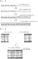
FIG. 1 is a flow chart illustrating a method for manufacturing a photomask according to one embodiment of the present specification. -
FIG. 2 is a plane figure illustrating a shielding mask pattern of a photomask according to one embodiment of the present specification. -
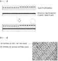
FIG. 3 is a flow chart illustrating a method for forming a pattern using a photomask according to one embodiment of the present specification. -
FIG. 4 is a pattern image prepared using a photomask according to one embodiment of the present specification. -
FIG. 5 is a flow chart illustrating a method for manufacturing a photomask of Comparative Example 1. -
FIG. 6 is a flow chart illustrating a method for manufacturing a photomask of Comparative Example 2. - Hereinafter, the present specification will be described in detail.
- One embodiment of the present specification provides a photomask including a first unit including a first shielding mask pattern provided on a first substrate; a second unit including a second shielding mask pattern provided on a second substrate; an intermediate layer located between a surface of the first unit provided with the first shielding mask pattern and a surface of the second unit provided with the second shielding mask pattern; and a transparent planarization layer located on a surface of the second unit opposite to the surface provided with the intermediate layer.
- The first unit may include a first shielding mask pattern provided on a first substrate, and the second unit may include a second shielding mask pattern provided on a second substrate.
- Materials of the first substrate and the second substrate are not particularly limited, however, those having favorable adhesion with the shielding mask pattern and the intermediate layer, and as a substrate of a photomask, those having a minimum influence on light penetrating the photomask are preferred.
- The first substrate and the second substrate may each be a hard substrate or a flexible substrate. Specifically, the flexible substrate may be a plastic substrate or a plastic film. The plastic substrate or the plastic film is not particularly limited, and examples thereof may include any one or more of polyacrylate, polypropylene (PP), polyethylene terephthalate (PET), polyethylene ether phthalate, polyethylene phthalate, polybuthylene phthalate, polyethylene naphthalate (PEN), polycarbonate (PC), polystyrene (PS), polyether imide, polyether sulfone, polydimethyl siloxane (PDMS), polyetheretherketone (PEEK) and polyimide (PI).
- As the first substrate and the second substrate, substrates having high transparency may be used, and light transmittance of the first substrate and the second substrate may be 50% or greater.
- A difference between the refractive index of each of the first substrate and the second substrate, and the refractive index of the intermediate layer is preferably small, and the refractive indexes of the first substrate and the second substrate may each be greater than or equal to 1.45 and less than or equal to 1.65.
- The first substrate and the second substrate may be formed with materials the same as or different from each other, however, the first substrate and the second substrate are preferably formed with the same material.
- A part of the first shielding mask pattern of the first unit may overlap with the second shielding mask pattern of the second unit, or the first shielding mask pattern of the first unit may not overlap with the second shielding mask pattern of the second unit. Specifically, a part of the first shielding mask pattern of the first unit may overlap with the second shielding mask pattern of the second unit.
- As illustrated in
FIG. 2 , a part of the first shielding mask pattern of the first unit may overlap with the second shielding mask pattern of the second unit. - The surface of the first unit provided with the first shielding mask pattern and the surface of the second unit provided with the second shielding mask pattern may face each other. As illustrated in
FIG. 1 , the surface of the first unit provided with the first shielding mask pattern and the surface of the second unit provided with the second shielding mask pattern may face each other. - The intermediate layer is located between the surface of the first unit provided with the first shielding mask pattern and the surface of the second unit provided with the second shielding mask pattern, preferably has adhesive strength capable of adhering the first unit and the second unit, and has a minimum influence on light penetrating the photomask.
- The intermediate layer may include a silicone-based resin, specifically may include a siloxane-based resin, and more specifically may include polydimethylsiloxane (PDMS).
- The intermediate layer may have a thickness of greater than or equal to 1 µm and less than or equal to 500 µm, however, the thickness is not limited thereto.
- The transparent planarization layer is located on a surface of the second unit opposite to the surface provided with the intermediate layer, and the surface of the second unit opposite to the surface provided with the intermediate layer is a flat layer. Of the transparent planarization layer, surface roughness (Ra) representing a degree of planarization of the surface of the second unit opposite to the surface provided with the intermediate layer is preferably greater than or equal to 0.1 nm and less than or equal to 20 nm.
- As the transparent planarization layer, those that are not shielded by the shielding mask pattern and having a minimum influence on light penetrating the photomask are preferred. Materials having high transparency may be used as the transparent planarization layer, and the transparent planarization layer may have light transmittance of 50% or greater.
- Differences between the refractive index of the transparent planarization layer and the refractive indexes of the first substrate, the second substrate and the intermediate layer are preferably small, and the refractive index of the transparent planarization layer may be greater than or equal to 1.43 and less than or equal to 1.49.
- The transparent planarization layer may have a thickness of greater than or equal to 1 µm and less than or equal to 500 µm. Specifically, the transparent planarization layer may have a thickness of greater than or equal to 1 µm and less than or equal to 50 µm.
- The transparent planarization layer preferably has an excellent coating property so as to form a flat layer, has high light transmittance, and has adhesive and releasing properties so as to be attached to and separated from surfaces of other materials.
- The transparent planarization layer may include a silicone-based resin, specifically, may include a siloxane-based resin, and more specifically, may include polydimethylsiloxane (PDMS).
- The transparent planarization layer may include a silicone-based resin the same as or different from the intermediate layer. The transparent planarization layer preferably includes the same silicone-based resin as the intermediate layer.
- Another embodiment of the present specification provides a laminate including an exposure target including a photoresist layer provided on a base plate; and a photomask including a first unit including a first shielding mask pattern provided on a first substrate, a second unit including a second shielding mask pattern provided on a second substrate, an intermediate layer located between a surface of the first unit provided with the first shielding mask pattern and a surface of the second unit provided with the second shielding mask pattern, and a transparent planarization layer located on a surface of the second unit opposite to the surface provided with the intermediate layer, wherein the photoresist layer of the exposure target is in contact with the transparent planarization layer of the photomask.
- Materials of the base plate are not particularly limited, however, the base plate may be a hard material or a soft material.
- The hard material may include glass, metals, hard plastics or thick plastics.
- The soft material may include soft plastics or thin plastics.
- The base plate may have a thickness of greater than or equal to 15 µm and less than or equal to 2 mm, however, the thickness is not limited thereto.
- The photoresist layer (PR) means a layer including a polymer with varying tolerance for a developing solution by being exposed to light, and the photoresist layer may be a positive photoresist layer or a negative photoresist layer. Specifically, the photoresist layer is preferably a positive photoresist layer.
- The photoresist layer may have a thickness of greater than or equal to 100 nm and less than or equal to 10 µm, however, the thickness is not limited thereto.
- The exposure target may further include a metal layer provided between the base plate and the photoresist layer.
- Materials of the metal layer are not particularly limited, however, the metal layer may be formed with at least one of copper (Cu), chromium (Cr), aluminum (Al), molybdenum (Mo), nickel (Ni), gold (Au) and silver (Ag).
- As for the descriptions on the photomask in the laminate, the description on the photomask provided above may be used.
- One embodiment of the present specification provides a method for manufacturing a photomask including preparing a first unit including a first shielding mask pattern provided on a first substrate and a second unit including a second shielding mask pattern provided on a second substrate; forming an intermediate layer on a surface of the first unit provided with the first shielding mask pattern and then laminating the second unit on the intermediate layer; and forming a transparent planarization layer on a surface of the second unit opposite to the surface provided with the intermediate layer.
- The method for manufacturing a photomask may include preparing a first unit including a first shielding mask pattern provided on a first substrate and a second unit including a second shielding mask pattern provided on a second substrate.
- The method of forming a first shielding mask pattern and a second shielding mask pattern on a first substrate and a second substrate, respectively, may each be inkjet printing, gravure printing, gravure offset printing, screen printing, reverse offset printing, and photolithography. Specifically, the method of forming a first shielding mask pattern and a second shielding mask pattern on a first substrate and a second substrate, respectively, may be photolithography, and after depositing shielding mask metals on a substrate and forming an etching resist pattern, the metals in a region that is not provided with the etching resist pattern are selectively removed through an etching process, and lastly, the etching resist pattern on the shielding mask pattern is peeled off to form the shielding mask pattern.
- As for descriptions on the first unit and the second unit, the descriptions provided above may be used.
- The method for manufacturing a photomask may include forming an intermediate layer on a surface of the first unit provided with the first shielding mask pattern and then laminating the second unit on the intermediate layer.
- The method of forming an intermediate layer may include coating a composition for forming an intermediate layer on a surface of the first unit provided with the first shielding mask pattern, and then drying and curing the composition.
- The laminating of the second unit on the intermediate layer may be laminating so that the second substrate of the second unit is in contact with the intermediate layer thereon, or laminating so that a surface of the second substrate of the second unit provided with the second shielding mask pattern is in contact with the intermediate layer thereon. Specifically, the laminating of the second unit on the intermediate layer is preferably laminating so that a surface of the second substrate of the second unit provided with the second shielding mask pattern is in contact with the intermediate layer thereon. In other words, the surface of the first unit provided with the first shielding mask pattern and the surface of the second unit provided with the second shielding mask pattern preferably face each other.
- The method for manufacturing a photomask may include forming a transparent planarization layer on a surface of the second unit opposite to the surface provided with the intermediate layer.
- The forming of a transparent planarization layer may include coating a composition for forming a transparent planarization layer on a surface of the second unit opposite to the surface provided with the intermediate layer; and drying and curing the composition. Herein, as the methods of coating, drying and curing may employ methods generally used in the art.
- The composition for forming a transparent planarization layer may include a silicone-based resin, specifically, may include a siloxane-based resin, and more specifically, include polydimethylsiloxane (PDMS).
- The composition for forming an intermediate layer and the composition for forming a transparent planarization layer may each include a silicone-based resin, and the composition for forming an intermediate layer may include a silicone-based resin the same as or different from the composition for forming a transparent planarization layer. The composition for forming an intermediate layer preferably includes the same silicone-based resin with the composition for forming a transparent planarization layer.
- The composition for forming an intermediate layer and the composition for forming a transparent planarization layer may each further include a curing agent. The curing agent is not particularly limited, and materials generally used in the art may be selected.
- One embodiment of the present specification provides a method for forming a pattern including preparing an exposure target including a photoresist layer provided on a base plate; laminating so that the photoresist layer of the exposure target is in contact with, in a photomask including a first unit including a first shielding mask pattern provided on a first substrate, a second unit including a second shielding mask pattern provided on a second substrate, an intermediate layer located between a surface of the first unit provided with the first shielding mask pattern and a surface of the second unit provided with the second shielding mask pattern, and a transparent planarization layer located on a surface of the second unit opposite to the surface provided with the intermediate layer, the transparent planarization layer of the photomask; exposing by irradiating light from a side of the first substrate of the photomask; and separating the photomask from the exposure target after the exposing.
- In the method for forming a pattern, descriptions duplicated with the descriptions provided above will not be repeated, and these may cite the descriptions provided above.
- The method for forming a pattern may further include forming a photoresist pattern by developing the exposed exposure target after separating the photomask.
- The method of developing the exposed exposure target may include forming a photoresist pattern by coating a developing solution on the exposed exposure target, or forming a photoresist pattern by immersing the exposed exposure target into a developing solution.
- When the exposure target further includes a metal layer provided between the base plate and the photoresist layer, the method for forming a pattern may further include forming a photoresist pattern by developing the exposed exposure target after separating the photomask; and forming a metal pattern by etching a part of the metal layer where the photoresist pattern is not formed.
- The forming of a metal pattern may include etching a part of the metal layer where the photoresist pattern is not formed; and removing the photoresist pattern after etching the metal layer.
- Hereinafter, the present specification will be described in more detail with reference to example. However, the following examples are for illustrative purposes only, and not to limit the present specification.
- On a surface of a first unit provided with a first shielding mask pattern having a size of 500 mmx500 mm, a silicone-based resin composition was coated to a thickness of 100 µm using a baker applicator, and the result was dried for 10 minutes at 70°C to finally form an intermediate layer having a thickness of 30 µm. As the silicone-based resin composition, a composition mixing a main substance (product name KE-1606) and a curing agent (product name CAT-RG) manufactured by Shin-Etsu Chemical Co., Ltd. in a ratio of 10:1.5 was used.
- On the intermediate layer, a surface of a second unit provided with a second shielding mask pattern having a size of 500 mmx500 mm was laminated so as to face each other.
- As the first unit and the second unit, an aluminum (Al) mesh pattern having a line width of 10 µm, line spacing of 300 µm and a line height of 100 nm was provided on a PET base plate having a thickness of 100 µm.
- On a surface of the second unit opposite to the surface provided with the intermediate layer, the silicone-based resin composition was coated to a thickness of 100 µm using a baker applicator, the result was dried and thermally cured for 10 minutes at 100°C to finally form a transparent planarization layer having a thickness of 30 µm, and a film photomask as in
FIG. 1 was manufactured. - On a PET base plate having a thickness of 100 µm, a positive photoresist formed with a novolac resin and a diazonaphthoquinone derivative was coated to a thickness of 1.5 µm using a slot die coater.
- The manufactured film photomask and the exposure target were laminated as in
FIG. 3 using a roll laminator. - After exposing the laminated laminate using a parallel light exposure apparatus provided with a collimation lens, the film photomask was separated from the exposure target, and the exposure target was immersed in a developing solution having a 2.38 wt% tetramethyl ammonium hydroxide (TMAH) concentration for 50 seconds to form a photoresist pattern.
- A film photomask was manufactured in the same manner as in Example 1 except that the mesh patterns of the first unit and the second unit were disposed so as to overlap as in
FIG. 4 , and a photoresist pattern was formed on the exposure target using the manufactured film photomask. - As a result, it was seen that line widths of the photoresist pattern formed by the first shielding mask pattern of the first unit and the photoresist pattern formed by the second shielding mask pattern of the second unit were the same as in
FIG. 4 . - A film photomask was manufactured in the same manner as in the examples except that the transparent planarization layer was not formed, and a structure of Comparative Example 1 is illustrated in
FIG. 5 . - When using Comparative Example 1, lifting occurred when the photomask and the photoresist of the printing target were brought into contact with each other, and surface contamination occurred.
- A film photomask was manufactured in the same manner as in the examples except that the intermediate layer was formed on a surface of the second unit opposite to the surface provided with the shielding pattern, and a structure of Comparative Example 2 is illustrated in
FIG. 6 . - When using Comparative Example 2, it was seen that line widths of the photoresist pattern formed by the first shielding pattern and the photoresist pattern formed by the second shielding pattern became different.
Claims (17)
- A photomask comprising:a first unit including a first shielding mask pattern provided on a first substrate;a second unit including a second shielding mask pattern provided on a second substrate;an intermediate layer located between a surface of the first unit provided with the first shielding mask pattern and a surface of the second unit provided with the second shielding mask pattern; anda transparent planarization layer located on a surface of the second unit opposite to the surface provided with the intermediate layer.
- The photomask of Claim 1, wherein a part of the first shielding mask pattern of the first unit overlaps with the second shielding mask pattern of the second unit.
- The photomask of Claim 1, wherein the first shielding mask pattern of the first unit does not overlap with the second shielding mask pattern of the second unit.
- The photomask of Claim 1, wherein the surface of the first unit provided with the first shielding mask pattern and the surface of the second unit provided with the second shielding mask pattern face each other.
- The photomask of Claim 1, wherein the intermediate layer and the transparent planarization layer each include a silicone-based resin.
- A laminate comprising:an exposure target including a photoresist layer provided on a base plate; anda photomask including a first unit including a first shielding mask pattern provided on a first substrate, a second unit including a second shielding mask pattern provided on a second substrate, an intermediate layer located between a surface of the first unit provided with the first shielding mask pattern and a surface of the second unit provided with the second shielding mask pattern, and a transparent planarization layer located on a surface of the second unit opposite to the surface provided with the intermediate layer,wherein the photoresist layer of the exposure target is in contact with the transparent planarization layer of the photomask.
- The laminate of Claim 6, wherein the photoresist layer is a positive photoresist layer.
- The laminate of Claim 6, wherein the exposure target further includes a metal layer provided between the base plate and the photoresist layer.
- The laminate of Claim 6, wherein a part of the first shielding mask pattern of the first unit overlaps with the second shielding mask pattern of the second unit.
- The laminate of Claim 6, wherein the first shielding mask pattern of the first unit does not overlap with the second shielding mask pattern of the second unit.
- The laminate of Claim 6, wherein the surface of the first unit provided with the first shielding mask pattern and the surface of the second unit provided with the second shielding mask pattern face each other.
- A method for manufacturing a photomask comprising:preparing a first unit including a first shielding mask pattern provided on a first substrate and a second unit including a second shielding mask pattern provided on a second substrate;forming an intermediate layer on a surface of the first unit provided with the first shielding mask pattern and then laminating the second unit on the intermediate layer; andforming a transparent planarization layer on a surface of the second unit opposite to the surface provided with the intermediate layer.
- The method for manufacturing a photomask of Claim 12, wherein the surface of the first unit provided with the first shielding mask pattern and the surface of the second unit provided with the second shielding mask pattern face each other.
- A method for forming a pattern comprising:preparing an exposure target including a photoresist layer provided on a base plate;laminating so that the photoresist layer of the exposure target is in contact with the transparent planarization layer of the photomask, which including a first unit including a first shielding mask pattern provided on a first substrate, a second unit including a second shielding mask pattern provided on a second substrate, an intermediate layer located between a surface of the first unit provided with the first shielding mask pattern and a surface of the second unit provided with the second shielding mask pattern, and a transparent planarization layer located on a surface of the second unit opposite to the surface provided with the intermediate layer;exposing by irradiating light from a side of the first substrate of the photomask; andseparating the photomask from the exposure target after the exposing.
- The method for forming a pattern of Claim 14, further comprising forming a photoresist pattern by developing the exposed exposure target after separating the photomask.
- The method for forming a pattern of Claim 14, wherein the exposure target further includes a metal layer provided between the base plate and the photoresist layer.
- The method for forming a pattern of Claim 16, further comprising:forming a photoresist pattern by developing the exposed exposure target after separating the photomask; andforming a metal pattern by etching a part of the metal layer where the photoresist pattern is not formed.
Applications Claiming Priority (2)
| Application Number | Priority Date | Filing Date | Title |
|---|---|---|---|
| KR1020150106833A KR102042872B1 (en) | 2015-07-28 | 2015-07-28 | Photomask, laminate comprising the photomask, method for manufacturing the photomask and device for forming pattern using the photomask |
| PCT/KR2016/008299 WO2017018831A1 (en) | 2015-07-28 | 2016-07-28 | Photomask, laminate comprising photomask, photomask preparation method, and pattern forming method using photomask |
Publications (3)
| Publication Number | Publication Date |
|---|---|
| EP3330795A1 true EP3330795A1 (en) | 2018-06-06 |
| EP3330795A4 EP3330795A4 (en) | 2019-03-27 |
| EP3330795B1 EP3330795B1 (en) | 2023-01-11 |
Family
ID=57884776
Family Applications (1)
| Application Number | Title | Priority Date | Filing Date |
|---|---|---|---|
| EP16830864.1A Active EP3330795B1 (en) | 2015-07-28 | 2016-07-28 | Photomask, laminate comprising photomask, photomask preparation method, and pattern forming method using photomask |
Country Status (6)
| Country | Link |
|---|---|
| US (1) | US10747101B2 (en) |
| EP (1) | EP3330795B1 (en) |
| JP (1) | JP6458972B2 (en) |
| KR (1) | KR102042872B1 (en) |
| CN (1) | CN107710071A (en) |
| WO (1) | WO2017018831A1 (en) |
Families Citing this family (1)
| Publication number | Priority date | Publication date | Assignee | Title |
|---|---|---|---|---|
| US11294273B2 (en) * | 2019-10-25 | 2022-04-05 | Innolux Corporation | Mask substrate and method for forming mask substrate |
Family Cites Families (23)
| Publication number | Priority date | Publication date | Assignee | Title |
|---|---|---|---|---|
| JPS5745979B2 (en) | 1973-05-09 | 1982-09-30 | ||
| JPS5950444A (en) | 1982-09-16 | 1984-03-23 | Tokyo Ohka Kogyo Co Ltd | Photomask for microfabrication |
| JPH0566554A (en) * | 1991-09-09 | 1993-03-19 | Sharp Corp | Photo mask |
| JPH0675358A (en) * | 1992-08-27 | 1994-03-18 | Oki Electric Ind Co Ltd | Production of photomask |
| US6300042B1 (en) * | 1998-11-24 | 2001-10-09 | Motorola, Inc. | Lithographic printing method using a low surface energy layer |
| JP2000292905A (en) * | 1999-04-12 | 2000-10-20 | Hitachi Ltd | Method of creating pattern data and method of manufacturing solid state device |
| JP2001296650A (en) * | 2000-04-17 | 2001-10-26 | Nec Corp | Reticle |
| KR100496520B1 (en) * | 2002-09-13 | 2005-06-22 | 주식회사 릿츠 | Stamper manufacturing method using photo lithography and stamper manufactured its method, and light guide panel manufactured using stamper |
| JP2005003949A (en) * | 2003-06-12 | 2005-01-06 | Renesas Technology Corp | Photomask and its manufacturing method |
| US20050100798A1 (en) * | 2003-10-15 | 2005-05-12 | Taiwan Semiconductor Manufacturing Company, Ltd. | Device and method for providing wavelength reduction with a photomask |
| US7259106B2 (en) * | 2004-09-10 | 2007-08-21 | Versatilis Llc | Method of making a microelectronic and/or optoelectronic circuitry sheet |
| KR20060079957A (en) | 2005-01-04 | 2006-07-07 | 삼성에스디아이 주식회사 | Flexible photomask for photolithography, manufacturing method thereof, pattern formation method employing the same |
| JP4563949B2 (en) * | 2005-10-21 | 2010-10-20 | 信越化学工業株式会社 | Mask pattern coating material |
| US7632609B2 (en) | 2005-10-24 | 2009-12-15 | Shin-Etsu Chemical Co., Ltd. | Fabrication method of photomask-blank |
| JP4204583B2 (en) * | 2005-10-24 | 2009-01-07 | 信越化学工業株式会社 | Photomask blank manufacturing method |
| KR20090003601A (en) | 2007-07-03 | 2009-01-12 | 주식회사 엘지화학 | Flexible photomask and its manufacturing method |
| US7858687B2 (en) | 2008-07-30 | 2010-12-28 | E.I. Du Pont De Nemours And Company | Polyimide resins for high temperature wear applications |
| JP2010107886A (en) * | 2008-10-31 | 2010-05-13 | Fujifilm Corp | Hard coat composition for photomask, photomask and method for producing the same |
| US20120094220A1 (en) * | 2009-06-20 | 2012-04-19 | Sharp Kabushiki Kaisha | Photo mask, photolithography method, substrate production method and display panel production method |
| KR101148099B1 (en) * | 2010-10-01 | 2012-05-23 | 엘지이노텍 주식회사 | Carrier tape for TAB-package and Manufacturing method thereof |
| JP5745979B2 (en) | 2011-09-16 | 2015-07-08 | 三菱電機株式会社 | Multiple view liquid crystal display |
| CN202886836U (en) * | 2012-11-14 | 2013-04-17 | 京东方科技集团股份有限公司 | Mask |
| US9304389B2 (en) * | 2013-10-31 | 2016-04-05 | United Microelectronics Corp. | Photomask and fabrication method thereof |
-
2015
- 2015-07-28 KR KR1020150106833A patent/KR102042872B1/en active Active
-
2016
- 2016-07-28 JP JP2017559568A patent/JP6458972B2/en active Active
- 2016-07-28 CN CN201680033687.6A patent/CN107710071A/en active Pending
- 2016-07-28 WO PCT/KR2016/008299 patent/WO2017018831A1/en not_active Ceased
- 2016-07-28 EP EP16830864.1A patent/EP3330795B1/en active Active
- 2016-07-28 US US15/580,241 patent/US10747101B2/en active Active
Also Published As
| Publication number | Publication date |
|---|---|
| CN107710071A (en) | 2018-02-16 |
| US10747101B2 (en) | 2020-08-18 |
| KR20170013750A (en) | 2017-02-07 |
| EP3330795A4 (en) | 2019-03-27 |
| KR102042872B1 (en) | 2019-11-08 |
| JP6458972B2 (en) | 2019-01-30 |
| JP2018521339A (en) | 2018-08-02 |
| WO2017018831A1 (en) | 2017-02-02 |
| EP3330795B1 (en) | 2023-01-11 |
| US20180164677A1 (en) | 2018-06-14 |
Similar Documents
| Publication | Publication Date | Title |
|---|---|---|
| CN107710072B (en) | Photomask, laminate including photomask, photomask manufacturing method, patterning device, and patterning method | |
| WO2009108771A2 (en) | Methods of patterning a conductor on a substrate | |
| SE535467C2 (en) | Method of printing product characteristics on a substrate sheet | |
| KR20090003601A (en) | Flexible photomask and its manufacturing method | |
| JP4832341B2 (en) | Printing plate manufacturing method | |
| US10747101B2 (en) | Photomask, laminate comprising photomask, photomask preparation method, and pattern forming method using photomask | |
| JP6418891B2 (en) | Screen mask and method for manufacturing screen mask | |
| KR102092993B1 (en) | Photomask, laminate comprising the photomask and method for manufacturing the photomask | |
| JP4588041B2 (en) | Printing plate manufacturing method using resin mold | |
| KR20190053427A (en) | A film mask and a method for preparing the same | |
| US8399179B2 (en) | High aspect ratio microstructures | |
| CN109980053A (en) | A kind of electrode preparation method and light emitting diode | |
| KR101964603B1 (en) | Photomask, laminate comprising the photomask, method for manufacturing the photomask and device for forming pattern using the photomask | |
| JP6358488B2 (en) | Method for producing offset printing cliché and offset printing cliché | |
| JP2021146513A (en) | Adhesion layer and metal mask using adhesion layer | |
| KR101550221B1 (en) | High signal to background metal enhanced fluorescence substrate, method for manufacturing substrate thereof, and the biochip using the substrate thereof | |
| CN105044902B (en) | Preparation method, the electrowetting display device of electrowetting display device substrate | |
| CN105278237B (en) | Photomask and method for manufacturing photomask | |
| KR101486712B1 (en) | Method of Producing a Three-Dimensional Metal Structure on Flexible Substrate | |
| Cavallini et al. | Preparation of tools for lithographically controlled wetting and soft lithography |
Legal Events
| Date | Code | Title | Description |
|---|---|---|---|
| STAA | Information on the status of an ep patent application or granted ep patent |
Free format text: STATUS: THE INTERNATIONAL PUBLICATION HAS BEEN MADE |
|
| PUAI | Public reference made under article 153(3) epc to a published international application that has entered the european phase |
Free format text: ORIGINAL CODE: 0009012 |
|
| STAA | Information on the status of an ep patent application or granted ep patent |
Free format text: STATUS: REQUEST FOR EXAMINATION WAS MADE |
|
| 17P | Request for examination filed |
Effective date: 20171110 |
|
| AK | Designated contracting states |
Kind code of ref document: A1 Designated state(s): AL AT BE BG CH CY CZ DE DK EE ES FI FR GB GR HR HU IE IS IT LI LT LU LV MC MK MT NL NO PL PT RO RS SE SI SK SM TR |
|
| AX | Request for extension of the european patent |
Extension state: BA ME |
|
| DAV | Request for validation of the european patent (deleted) | ||
| DAX | Request for extension of the european patent (deleted) | ||
| A4 | Supplementary search report drawn up and despatched |
Effective date: 20190222 |
|
| RIC1 | Information provided on ipc code assigned before grant |
Ipc: G03F 1/48 20120101ALI20190218BHEP Ipc: G03F 1/38 20120101AFI20190218BHEP |
|
| STAA | Information on the status of an ep patent application or granted ep patent |
Free format text: STATUS: EXAMINATION IS IN PROGRESS |
|
| 17Q | First examination report despatched |
Effective date: 20210329 |
|
| GRAP | Despatch of communication of intention to grant a patent |
Free format text: ORIGINAL CODE: EPIDOSNIGR1 |
|
| STAA | Information on the status of an ep patent application or granted ep patent |
Free format text: STATUS: GRANT OF PATENT IS INTENDED |
|
| INTG | Intention to grant announced |
Effective date: 20221102 |
|
| GRAS | Grant fee paid |
Free format text: ORIGINAL CODE: EPIDOSNIGR3 |
|
| GRAA | (expected) grant |
Free format text: ORIGINAL CODE: 0009210 |
|
| STAA | Information on the status of an ep patent application or granted ep patent |
Free format text: STATUS: THE PATENT HAS BEEN GRANTED |
|
| AK | Designated contracting states |
Kind code of ref document: B1 Designated state(s): AL AT BE BG CH CY CZ DE DK EE ES FI FR GB GR HR HU IE IS IT LI LT LU LV MC MK MT NL NO PL PT RO RS SE SI SK SM TR |
|
| REG | Reference to a national code |
Ref country code: GB Ref legal event code: FG4D |
|
| REG | Reference to a national code |
Ref country code: CH Ref legal event code: EP |
|
| REG | Reference to a national code |
Ref country code: DE Ref legal event code: R096 Ref document number: 602016077421 Country of ref document: DE |
|
| REG | Reference to a national code |
Ref country code: IE Ref legal event code: FG4D |
|
| REG | Reference to a national code |
Ref country code: AT Ref legal event code: REF Ref document number: 1543781 Country of ref document: AT Kind code of ref document: T Effective date: 20230215 |
|
| REG | Reference to a national code |
Ref country code: LT Ref legal event code: MG9D |
|
| REG | Reference to a national code |
Ref country code: NL Ref legal event code: MP Effective date: 20230111 |
|
| REG | Reference to a national code |
Ref country code: AT Ref legal event code: MK05 Ref document number: 1543781 Country of ref document: AT Kind code of ref document: T Effective date: 20230111 |
|
| PG25 | Lapsed in a contracting state [announced via postgrant information from national office to epo] |
Ref country code: NL Free format text: LAPSE BECAUSE OF FAILURE TO SUBMIT A TRANSLATION OF THE DESCRIPTION OR TO PAY THE FEE WITHIN THE PRESCRIBED TIME-LIMIT Effective date: 20230111 |
|
| PG25 | Lapsed in a contracting state [announced via postgrant information from national office to epo] |
Ref country code: RS Free format text: LAPSE BECAUSE OF FAILURE TO SUBMIT A TRANSLATION OF THE DESCRIPTION OR TO PAY THE FEE WITHIN THE PRESCRIBED TIME-LIMIT Effective date: 20230111 Ref country code: PT Free format text: LAPSE BECAUSE OF FAILURE TO SUBMIT A TRANSLATION OF THE DESCRIPTION OR TO PAY THE FEE WITHIN THE PRESCRIBED TIME-LIMIT Effective date: 20230511 Ref country code: NO Free format text: LAPSE BECAUSE OF FAILURE TO SUBMIT A TRANSLATION OF THE DESCRIPTION OR TO PAY THE FEE WITHIN THE PRESCRIBED TIME-LIMIT Effective date: 20230411 Ref country code: LV Free format text: LAPSE BECAUSE OF FAILURE TO SUBMIT A TRANSLATION OF THE DESCRIPTION OR TO PAY THE FEE WITHIN THE PRESCRIBED TIME-LIMIT Effective date: 20230111 Ref country code: LT Free format text: LAPSE BECAUSE OF FAILURE TO SUBMIT A TRANSLATION OF THE DESCRIPTION OR TO PAY THE FEE WITHIN THE PRESCRIBED TIME-LIMIT Effective date: 20230111 Ref country code: HR Free format text: LAPSE BECAUSE OF FAILURE TO SUBMIT A TRANSLATION OF THE DESCRIPTION OR TO PAY THE FEE WITHIN THE PRESCRIBED TIME-LIMIT Effective date: 20230111 Ref country code: ES Free format text: LAPSE BECAUSE OF FAILURE TO SUBMIT A TRANSLATION OF THE DESCRIPTION OR TO PAY THE FEE WITHIN THE PRESCRIBED TIME-LIMIT Effective date: 20230111 Ref country code: AT Free format text: LAPSE BECAUSE OF FAILURE TO SUBMIT A TRANSLATION OF THE DESCRIPTION OR TO PAY THE FEE WITHIN THE PRESCRIBED TIME-LIMIT Effective date: 20230111 |
|
| PG25 | Lapsed in a contracting state [announced via postgrant information from national office to epo] |
Ref country code: SE Free format text: LAPSE BECAUSE OF FAILURE TO SUBMIT A TRANSLATION OF THE DESCRIPTION OR TO PAY THE FEE WITHIN THE PRESCRIBED TIME-LIMIT Effective date: 20230111 Ref country code: PL Free format text: LAPSE BECAUSE OF FAILURE TO SUBMIT A TRANSLATION OF THE DESCRIPTION OR TO PAY THE FEE WITHIN THE PRESCRIBED TIME-LIMIT Effective date: 20230111 Ref country code: IS Free format text: LAPSE BECAUSE OF FAILURE TO SUBMIT A TRANSLATION OF THE DESCRIPTION OR TO PAY THE FEE WITHIN THE PRESCRIBED TIME-LIMIT Effective date: 20230511 Ref country code: GR Free format text: LAPSE BECAUSE OF FAILURE TO SUBMIT A TRANSLATION OF THE DESCRIPTION OR TO PAY THE FEE WITHIN THE PRESCRIBED TIME-LIMIT Effective date: 20230412 Ref country code: FI Free format text: LAPSE BECAUSE OF FAILURE TO SUBMIT A TRANSLATION OF THE DESCRIPTION OR TO PAY THE FEE WITHIN THE PRESCRIBED TIME-LIMIT Effective date: 20230111 |
|
| REG | Reference to a national code |
Ref country code: DE Ref legal event code: R097 Ref document number: 602016077421 Country of ref document: DE |
|
| PG25 | Lapsed in a contracting state [announced via postgrant information from national office to epo] |
Ref country code: SM Free format text: LAPSE BECAUSE OF FAILURE TO SUBMIT A TRANSLATION OF THE DESCRIPTION OR TO PAY THE FEE WITHIN THE PRESCRIBED TIME-LIMIT Effective date: 20230111 Ref country code: RO Free format text: LAPSE BECAUSE OF FAILURE TO SUBMIT A TRANSLATION OF THE DESCRIPTION OR TO PAY THE FEE WITHIN THE PRESCRIBED TIME-LIMIT Effective date: 20230111 Ref country code: EE Free format text: LAPSE BECAUSE OF FAILURE TO SUBMIT A TRANSLATION OF THE DESCRIPTION OR TO PAY THE FEE WITHIN THE PRESCRIBED TIME-LIMIT Effective date: 20230111 Ref country code: DK Free format text: LAPSE BECAUSE OF FAILURE TO SUBMIT A TRANSLATION OF THE DESCRIPTION OR TO PAY THE FEE WITHIN THE PRESCRIBED TIME-LIMIT Effective date: 20230111 Ref country code: CZ Free format text: LAPSE BECAUSE OF FAILURE TO SUBMIT A TRANSLATION OF THE DESCRIPTION OR TO PAY THE FEE WITHIN THE PRESCRIBED TIME-LIMIT Effective date: 20230111 |
|
| PLBE | No opposition filed within time limit |
Free format text: ORIGINAL CODE: 0009261 |
|
| STAA | Information on the status of an ep patent application or granted ep patent |
Free format text: STATUS: NO OPPOSITION FILED WITHIN TIME LIMIT |
|
| PG25 | Lapsed in a contracting state [announced via postgrant information from national office to epo] |
Ref country code: SK Free format text: LAPSE BECAUSE OF FAILURE TO SUBMIT A TRANSLATION OF THE DESCRIPTION OR TO PAY THE FEE WITHIN THE PRESCRIBED TIME-LIMIT Effective date: 20230111 |
|
| 26N | No opposition filed |
Effective date: 20231012 |
|
| PG25 | Lapsed in a contracting state [announced via postgrant information from national office to epo] |
Ref country code: SI Free format text: LAPSE BECAUSE OF FAILURE TO SUBMIT A TRANSLATION OF THE DESCRIPTION OR TO PAY THE FEE WITHIN THE PRESCRIBED TIME-LIMIT Effective date: 20230111 |
|
| PG25 | Lapsed in a contracting state [announced via postgrant information from national office to epo] |
Ref country code: MC Free format text: LAPSE BECAUSE OF FAILURE TO SUBMIT A TRANSLATION OF THE DESCRIPTION OR TO PAY THE FEE WITHIN THE PRESCRIBED TIME-LIMIT Effective date: 20230111 |
|
| PG25 | Lapsed in a contracting state [announced via postgrant information from national office to epo] |
Ref country code: MC Free format text: LAPSE BECAUSE OF FAILURE TO SUBMIT A TRANSLATION OF THE DESCRIPTION OR TO PAY THE FEE WITHIN THE PRESCRIBED TIME-LIMIT Effective date: 20230111 |
|
| REG | Reference to a national code |
Ref country code: CH Ref legal event code: PL |
|
| REG | Reference to a national code |
Ref country code: BE Ref legal event code: MM Effective date: 20230731 |
|
| PG25 | Lapsed in a contracting state [announced via postgrant information from national office to epo] |
Ref country code: LU Free format text: LAPSE BECAUSE OF NON-PAYMENT OF DUE FEES Effective date: 20230728 |
|
| PG25 | Lapsed in a contracting state [announced via postgrant information from national office to epo] |
Ref country code: LU Free format text: LAPSE BECAUSE OF NON-PAYMENT OF DUE FEES Effective date: 20230728 |
|
| REG | Reference to a national code |
Ref country code: IE Ref legal event code: MM4A |
|
| PG25 | Lapsed in a contracting state [announced via postgrant information from national office to epo] |
Ref country code: CH Free format text: LAPSE BECAUSE OF NON-PAYMENT OF DUE FEES Effective date: 20230731 |
|
| PG25 | Lapsed in a contracting state [announced via postgrant information from national office to epo] |
Ref country code: IT Free format text: LAPSE BECAUSE OF FAILURE TO SUBMIT A TRANSLATION OF THE DESCRIPTION OR TO PAY THE FEE WITHIN THE PRESCRIBED TIME-LIMIT Effective date: 20230111 Ref country code: BE Free format text: LAPSE BECAUSE OF NON-PAYMENT OF DUE FEES Effective date: 20230731 |
|
| PG25 | Lapsed in a contracting state [announced via postgrant information from national office to epo] |
Ref country code: IE Free format text: LAPSE BECAUSE OF NON-PAYMENT OF DUE FEES Effective date: 20230728 |
|
| PG25 | Lapsed in a contracting state [announced via postgrant information from national office to epo] |
Ref country code: IE Free format text: LAPSE BECAUSE OF NON-PAYMENT OF DUE FEES Effective date: 20230728 |
|
| PG25 | Lapsed in a contracting state [announced via postgrant information from national office to epo] |
Ref country code: BG Free format text: LAPSE BECAUSE OF FAILURE TO SUBMIT A TRANSLATION OF THE DESCRIPTION OR TO PAY THE FEE WITHIN THE PRESCRIBED TIME-LIMIT Effective date: 20230111 |
|
| PG25 | Lapsed in a contracting state [announced via postgrant information from national office to epo] |
Ref country code: BG Free format text: LAPSE BECAUSE OF FAILURE TO SUBMIT A TRANSLATION OF THE DESCRIPTION OR TO PAY THE FEE WITHIN THE PRESCRIBED TIME-LIMIT Effective date: 20230111 |
|
| PGFP | Annual fee paid to national office [announced via postgrant information from national office to epo] |
Ref country code: GB Payment date: 20250624 Year of fee payment: 10 |
|
| PGFP | Annual fee paid to national office [announced via postgrant information from national office to epo] |
Ref country code: FR Payment date: 20250624 Year of fee payment: 10 |
|
| PG25 | Lapsed in a contracting state [announced via postgrant information from national office to epo] |
Ref country code: CY Free format text: LAPSE BECAUSE OF FAILURE TO SUBMIT A TRANSLATION OF THE DESCRIPTION OR TO PAY THE FEE WITHIN THE PRESCRIBED TIME-LIMIT; INVALID AB INITIO Effective date: 20160728 |
|
| PG25 | Lapsed in a contracting state [announced via postgrant information from national office to epo] |
Ref country code: HU Free format text: LAPSE BECAUSE OF FAILURE TO SUBMIT A TRANSLATION OF THE DESCRIPTION OR TO PAY THE FEE WITHIN THE PRESCRIBED TIME-LIMIT; INVALID AB INITIO Effective date: 20160728 |
|
| PGFP | Annual fee paid to national office [announced via postgrant information from national office to epo] |
Ref country code: DE Payment date: 20250624 Year of fee payment: 10 |
|
| PG25 | Lapsed in a contracting state [announced via postgrant information from national office to epo] |
Ref country code: TR Free format text: LAPSE BECAUSE OF FAILURE TO SUBMIT A TRANSLATION OF THE DESCRIPTION OR TO PAY THE FEE WITHIN THE PRESCRIBED TIME-LIMIT Effective date: 20230111 |