EP3329363B1 - Vector arithmethic instruction - Google Patents
Vector arithmethic instruction Download PDFInfo
- Publication number
- EP3329363B1 EP3329363B1 EP16732707.1A EP16732707A EP3329363B1 EP 3329363 B1 EP3329363 B1 EP 3329363B1 EP 16732707 A EP16732707 A EP 16732707A EP 3329363 B1 EP3329363 B1 EP 3329363B1
- Authority
- EP
- European Patent Office
- Prior art keywords
- vector
- source operand
- elements
- bit size
- operand
- Prior art date
- Legal status (The legal status is an assumption and is not a legal conclusion. Google has not performed a legal analysis and makes no representation as to the accuracy of the status listed.)
- Active
Links
Images


Classifications
-
- G—PHYSICS
- G06—COMPUTING OR CALCULATING; COUNTING
- G06F—ELECTRIC DIGITAL DATA PROCESSING
- G06F9/00—Arrangements for program control, e.g. control units
- G06F9/06—Arrangements for program control, e.g. control units using stored programs, i.e. using an internal store of processing equipment to receive or retain programs
- G06F9/30—Arrangements for executing machine instructions, e.g. instruction decode
- G06F9/30003—Arrangements for executing specific machine instructions
- G06F9/30007—Arrangements for executing specific machine instructions to perform operations on data operands
- G06F9/30036—Instructions to perform operations on packed data, e.g. vector, tile or matrix operations
- G06F9/30038—Instructions to perform operations on packed data, e.g. vector, tile or matrix operations using a mask
-
- G—PHYSICS
- G06—COMPUTING OR CALCULATING; COUNTING
- G06F—ELECTRIC DIGITAL DATA PROCESSING
- G06F17/00—Digital computing or data processing equipment or methods, specially adapted for specific functions
- G06F17/10—Complex mathematical operations
- G06F17/16—Matrix or vector computation, e.g. matrix-matrix or matrix-vector multiplication, matrix factorization
-
- G—PHYSICS
- G06—COMPUTING OR CALCULATING; COUNTING
- G06F—ELECTRIC DIGITAL DATA PROCESSING
- G06F9/00—Arrangements for program control, e.g. control units
- G06F9/06—Arrangements for program control, e.g. control units using stored programs, i.e. using an internal store of processing equipment to receive or retain programs
- G06F9/30—Arrangements for executing machine instructions, e.g. instruction decode
- G06F9/30003—Arrangements for executing specific machine instructions
- G06F9/30007—Arrangements for executing specific machine instructions to perform operations on data operands
- G06F9/3001—Arithmetic instructions
- G06F9/30014—Arithmetic instructions with variable precision
-
- G—PHYSICS
- G06—COMPUTING OR CALCULATING; COUNTING
- G06F—ELECTRIC DIGITAL DATA PROCESSING
- G06F9/00—Arrangements for program control, e.g. control units
- G06F9/06—Arrangements for program control, e.g. control units using stored programs, i.e. using an internal store of processing equipment to receive or retain programs
- G06F9/30—Arrangements for executing machine instructions, e.g. instruction decode
- G06F9/30003—Arrangements for executing specific machine instructions
- G06F9/30007—Arrangements for executing specific machine instructions to perform operations on data operands
- G06F9/30036—Instructions to perform operations on packed data, e.g. vector, tile or matrix operations
Definitions
- This disclosure relates to the field of data processing systems. More particularly, this disclosure relates to data processing systems supporting vector arithmetic instructions.
- a vector arithmetic instruction may take two such vector input operands and perform an arithmetic operation specified by the instruction upon respective pairs of vector elements from within the two vector operands.
- Vector processing facilitates parallel computation.
- US2005/0240870 A1 discloses a SIMD mixed mode instruction taking as input a set of four 16-bit operands and a set of 8 eight-bit operands.
- US2005/0125361 A1 discloses a vector by scalar SIMD instruction wherein each of the operands of a first input vector are subjected to an arithmetic operation with a second source operand element storing a scalar value.
- Figure 1 schematically illustrates a data processing system 2 comprising a processor 4 coupled to a memory 6.
- the memory 6 stores data values 8 to the manipulated and program instructions 10 specifying data processing operations to be performed by the processor 4.
- Program instructions 10 are fetched by an instruction fetch unit 12 and passed to decoder circuitry 14.
- the decoder circuitry 14 generates control signals 16 which serve to control processing circuitry 18, 20, 22, 24 within the processor 4 to perform processing operations specified by the decoded instructions.
- the processor 4 supports both vector operations and scalar operations.
- Vector processing circuitry 18 acting upon vector operands stored within a vector register file 22 serves to perform vector processing operations.
- Scalar processing circuitry 20 acting upon scalar operand values stored within a scalar register file 24 serves to perform scalar processing operations.
- vector processing operations can take a variety of different forms. For example, SIMD (Single Instruction Multiple Data) processing operations are one form of vector processing operation. More generally, a vector processing operation is performed upon a plurality of vector elements which together formed a vector operand.
- a vector operand of 256 bits in length may be formed of 16 vector elements each of 16 bits of length.
- the processing operations performed upon the individual vector elements will typically be performed at least partially in parallel, but this need not always be the case.
- Scalar processing operations are performed with input operands comprising a single value, e.g. 64-bit scalar processing operations may be performed upon two 64-bit scalar input operands and generate a 64-bit scalar output operand.
- the vector processing circuitry 18 is formed in accordance with the present disclosure to support at least one mixed-element-sized vector arithmetic instruction performed under control of control signal 16 generated by decoder circuitry 14 when a mixed-element-sized vector arithmetic instruction is fetched, decoded and executed.
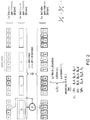
- Figure 2 schematically illustrates the operation and assembler syntax of a mixed-element-sized vector arithmetic instruction.
- the mixed-element-sized vector arithmetic instruction performs an arithmetic processing operation, such as a logical shift, a division, or a compare, upon a first vector of first source operand elements a i .
- an arithmetic processing operation such as a logical shift, a division, or a compare
- first vector of first source operand elements a i there are sixteen first source operand elements a 0 -a 15 .
- Each of these first source operand elements a i has a bit size of A.
- 16 first source operand elements a i are arranged into 4 disjoint subsets a 0 -a 3 , a 4 -a 7 , a 8 -a 11 , and a 12 -a 15.
- the mixed-element-sized vector arithmetic instruction has a second vector of second source operand elements b i .
- the second vector of second source operand elements is formed of four second source operand elements namely second source operand elements b 0 -b 3 , each of bit size B.
- first source operand elements and four second source operand elements there are sixteen first source operand elements and four second source operand elements, more generally there may be N first source operand elements and M and second source operand elements.
- the second source operand elements have a greater bit size B than the first source operand elements bit size A.
- the ratio of the bit size B of the second source operand elements to the bit size A of the first source operand elements may be 4:1. This is the same as the ratio of the number of first source operand elements N to the number of second source operand elements M.
- each of the disjoint subsets of first source operand elements is subject to an arithmetic processing operation with a respective one of the second source operand elements being the second operand input. More particularly, first source operand elements a 1 -a 3 are subject to an arithmetic processing operation with the second source operand element b 0 being the second input to that arithmetic processing operation. For example, each of the first source operand elements a 0 -a 3 may be separately subjected to a logical shift right by a shift amount specified by the second source operand element b 0 . The resulting output operand has the same bit size A as the first source operand elements.
- arithmetic processing operations may be performed for the mixed-element-sized vector arithmetic instruction e.g. a first source operand element a i being divided by a corresponding second source operand element b j or a first source operand element a i being subjected to a compare (subtract) with a corresponding second source operand element b j .
- the arithmetic processing operation such as a logical shift, divide or compare is specified by a mnenonic such as LSR, DIV or CMP.
- the instruction specifies an element size for the first source operand elements, namely whether these are bytes B, half words. H, words W, or double words D. In the case of 64-bit double words D, a 512 bit vector operand would contain 8 such double words.
- the second source operand elements in such a case may be for example, 128-bit vector elements with two of the double word first source operand elements being associated with each of the 128-bit second source operand elements. It will be understood that many other different total vector sizes and vector element sizes may be employed depending upon the implementation and the requirements of the particular instruction set or the processing performed.
- the syntax of the mixed-element-sized vector arithmetic instructions continues by specifying the destination vector register Z D together with its element bit size A. This is followed by specifying the vector register of the first source operand namely Z s1 together with its element bit size A. Finally, the vector register Z S2 of the second source operand together with their element bit size B is specified. This is an example of a mixed-element-sized vector arithmetic instruction having two input operands and one output operand.
- two input operands may be specified with the result being written to a predicate register P D which contains a "true” or a "false” result corresponding to the result of comparing each element in Z S1 with the wider elements in Z S2 (subtraction).
- the processing operation is a shift operation that shifts a first source operand element by a shift amount specified by a corresponding second source operand element.
- the arithmetic processing operation is a division operation that divides a first source operand element by a divisor specified by the corresponding second source operand element.
- the arithmetic processing operation is a compare operation that compares a first source operand element with a corresponding second source operand element.
- the element bit size of the first source operand elements is specified by an element size field "x", as mentioned above, which specifies whether the first source operand elements have the size of 8 bits, 16 bits, 32 bits or 64 bits.
- the second source operand elements may in some example embodiments have a bit size specified by a field within the mixed-element-sized instruction. However, in other example embodiments, such as the one illustrated in Figure 2 , the second source operand elements may have a fixed size, such as 64 bits or 128 bits. The first source operand elements are smaller in bit size then the second source elements. If the second source operand elements have a bit size of 64, then the first source operand elements will have a bit size of one of 8, 16 or 32.
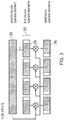
- Figure 3 schematically illustrates how an arithmetic instruction operates such that bit values 26 within a destination operand element are set in dependence upon one or more bit values of different bit significance within at least one of a corresponding first operand element 28 and second source operand element 30.
- bit positions 26 in the destination operand D i are dependent upon corresponding bits 29 having a higher order significance within the first source operand element 28 together with all of the bits 31 within the second source operand 30 which specify the right shift amount to be applied.
- the present disclosure teaches a system in which mixed-element-sized vector arithmetic instructions are supported. This is counter to the normal technical prejudice in this field. Normally all source operands for an arithmetic instruction all have a common element size. The present disclosure recognises that in certain circumstances the provision of mixed-element-sized vector arithmetic instructions provides advantages which justify the instruction bit space that such instructions consume within the instruction sets supported by the processor 4 and decoded by the decoder circuitry 14. When performing multiple operations of a program loop in parallel and that program loop has a scalar value operand, mixed-element-sized vector arithmetic instructions may be used to store copies of that scalar operand not sharing the same bit size as the first source operand elements for respective operations of the loop.
- the provision of mixed-element-sized vector arithmetic instructions may avoid the need to copy a scalar operand from the scalar register file 24 to the vector processing circuitry 18 upon each loop iteration, which can be a relatively slow process compared to the vector processing circuitry 18 accessing the vector register file 22 to which it is more directly coupled.
- one use of the mixed-element-sized vector arithmetic instructions provided by the present disclosure is to copy a scalar operand value which contains more significant bits than the first source vector elements from the scalar register file 24 to each of the wider second source operand elements within a second vector operand.
- the second vector can then be used as one of the vector operand inputs to a mixed-element-sized vector arithmetic instruction which operates on a plurality of first source vector operand elements using the wider second source operand elements into which the scalar operand has been copied.
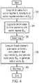
- FIG. 4 is a flow diagram schematically illustrating one example of the above type of operation.
- a 64-bit value from a scalar register X i is directly copied to all vector register elements of vector operand Z S2 .
- Step 34 then duplicates this 64-bit value from the vector register element to which is has been copied across all of the other vector register elements of the second vector.
- a processing loop which is to be performed is entered.
- Step 38 executes mixed-element-sized vector arithmetic instructions on a first input vector Z S1 and a second input vector Z s2 to generate an output vector Z D .
- the multiple copies of the scalar register are present within appropriate elements of the second vector and accordingly do not need to be moved from the scalar register file 24 to the vector register file 22 as the processing proceeds.
- the looping executed is exited.
- first source operand elements a i and second source operand elements b j i.e. a disjoint subset arrangement whereby each disjoint subset of the first source operand elements has a single associated second source operand element. It will be appreciated that in some embodiments such a division of the first source operand elements and association with the second source operand elements need not be provided.
- the above example discusses arithmetic processing operations in the form of shift operations, division operations and compare operations. It will be appreciated that other forms of arithmetic operation may also be supported.
- the operands acted upon by the arithmetic operations may be binary number values where each bit has different positional significance such that the first source operand elements contain binary number values, the second source operand elements contain binary number values and the destination operand elements contain destination operand binary number values.
- the processing operation is performed on the binary number values as a whole rather than independent bitwise operations performed independently of other bits at different positions (such as OR, XOR or AND).
- Figure 5 illustrates a virtual machine implementation that may be used. Whilst the earlier described embodiments implement the present invention in terms of apparatus and methods for operating specific processing hardware supporting the techniques concerned, it is also possible to provide so-called virtual machine implementations of hardware devices. These virtual machine implementations run on a host processor 530 running a host operating system 520 supporting a virtual machine program 510. Typically, large powerful processors are required to provide virtual machine implementations which execute at a reasonable speed, but such an approach may be justified in certain circumstances, such as when there is a desire to run code native to another processor for compatibility or re-use reasons.
- the virtual machine program 510 provides an application program interface to an application program 500 which is the same as the application program interface which would be provided by the real hardware which is the device being modelled by the virtual machine program 510.
- the program instructions including the control of memory accesses described above, may be executed from within the application program 500 using the virtual machine program 510 to model their interaction with the virtual machine hardware.
Landscapes
- Engineering & Computer Science (AREA)
- Physics & Mathematics (AREA)
- Theoretical Computer Science (AREA)
- Software Systems (AREA)
- General Physics & Mathematics (AREA)
- General Engineering & Computer Science (AREA)
- Mathematical Physics (AREA)
- Computational Mathematics (AREA)
- Pure & Applied Mathematics (AREA)
- Mathematical Optimization (AREA)
- Mathematical Analysis (AREA)
- Data Mining & Analysis (AREA)
- Algebra (AREA)
- Databases & Information Systems (AREA)
- Computing Systems (AREA)
- Complex Calculations (AREA)
- Advance Control (AREA)
- Executing Machine-Instructions (AREA)
Applications Claiming Priority (2)
| Application Number | Priority Date | Filing Date | Title |
|---|---|---|---|
| GB1513511.4A GB2540943B (en) | 2015-07-31 | 2015-07-31 | Vector arithmetic instruction |
| PCT/GB2016/051868 WO2017021681A1 (en) | 2015-07-31 | 2016-06-23 | Vector arithmethic instruction |
Publications (2)
| Publication Number | Publication Date |
|---|---|
| EP3329363A1 EP3329363A1 (en) | 2018-06-06 |
| EP3329363B1 true EP3329363B1 (en) | 2020-10-14 |
Family
ID=54062956
Family Applications (1)
| Application Number | Title | Priority Date | Filing Date |
|---|---|---|---|
| EP16732707.1A Active EP3329363B1 (en) | 2015-07-31 | 2016-06-23 | Vector arithmethic instruction |
Country Status (9)
| Country | Link |
|---|---|
| US (1) | US11003447B2 (enExample) |
| EP (1) | EP3329363B1 (enExample) |
| JP (1) | JP7071913B2 (enExample) |
| KR (1) | KR102584001B1 (enExample) |
| CN (1) | CN107851016B (enExample) |
| GB (1) | GB2540943B (enExample) |
| IL (1) | IL256663B (enExample) |
| TW (1) | TWI739754B (enExample) |
| WO (1) | WO2017021681A1 (enExample) |
Families Citing this family (7)
| Publication number | Priority date | Publication date | Assignee | Title |
|---|---|---|---|---|
| CN111651203B (zh) * | 2016-04-26 | 2024-05-07 | 中科寒武纪科技股份有限公司 | 一种用于执行向量四则运算的装置和方法 |
| EP3428792B1 (en) * | 2017-07-10 | 2022-05-04 | Arm Ltd | Testing bit values inside vector elements |
| JP6604393B2 (ja) * | 2018-03-08 | 2019-11-13 | 日本電気株式会社 | ベクトルプロセッサ、演算実行方法、プログラム |
| US10528346B2 (en) * | 2018-03-29 | 2020-01-07 | Intel Corporation | Instructions for fused multiply-add operations with variable precision input operands |
| US20210389948A1 (en) * | 2020-06-10 | 2021-12-16 | Arm Limited | Mixed-element-size instruction |
| US12182570B2 (en) * | 2021-06-25 | 2024-12-31 | Intel Corporation | Apparatuses, methods, and systems for a packed data convolution instruction with shift control and width control |
| CN114296798B (zh) * | 2021-12-10 | 2024-08-13 | 龙芯中科技术股份有限公司 | 向量移位方法、处理器及电子设备 |
Family Cites Families (20)
| Publication number | Priority date | Publication date | Assignee | Title |
|---|---|---|---|---|
| US6408320B1 (en) * | 1998-01-27 | 2002-06-18 | Texas Instruments Incorporated | Instruction set architecture with versatile adder carry control |
| US6282634B1 (en) * | 1998-05-27 | 2001-08-28 | Arm Limited | Apparatus and method for processing data having a mixed vector/scalar register file |
| GB2409068A (en) * | 2003-12-09 | 2005-06-15 | Advanced Risc Mach Ltd | Data element size control within parallel lanes of processing |
| US8082419B2 (en) * | 2004-03-30 | 2011-12-20 | Intel Corporation | Residual addition for video software techniques |
| ATE493703T1 (de) * | 2004-11-03 | 2011-01-15 | Koninkl Philips Electronics Nv | Programmierbare datenverarbeitungsschaltung, die simd-befehle unterstützt |
| US20080091924A1 (en) * | 2006-10-13 | 2008-04-17 | Jouppi Norman P | Vector processor and system for vector processing |
| GB2464292A (en) * | 2008-10-08 | 2010-04-14 | Advanced Risc Mach Ltd | SIMD processor circuit for performing iterative SIMD multiply-accumulate operations |
| GB2474901B (en) * | 2009-10-30 | 2015-01-07 | Advanced Risc Mach Ltd | Apparatus and method for performing multiply-accumulate operations |
| JP5699554B2 (ja) * | 2010-11-11 | 2015-04-15 | 富士通株式会社 | ベクトル処理回路、命令発行制御方法、及びプロセッサシステム |
| GB2488985A (en) * | 2011-03-08 | 2012-09-19 | Advanced Risc Mach Ltd | Mixed size data processing operation with integrated operand conversion instructions |
| WO2013095658A1 (en) | 2011-12-23 | 2013-06-27 | Intel Corporation | Systems, apparatuses, and methods for performing a horizontal add or subtract in response to a single instruction |
| CN104081336B (zh) | 2011-12-23 | 2018-10-23 | 英特尔公司 | 用于检测向量寄存器内的相同元素的装置和方法 |
| CN104185837B (zh) * | 2011-12-23 | 2017-10-13 | 英特尔公司 | 在不同的粒度等级下广播数据值的指令执行单元 |
| CN104137055B (zh) * | 2011-12-29 | 2018-06-05 | 英特尔公司 | 点积处理器、方法、系统和指令 |
| DE112012007058T5 (de) * | 2012-12-19 | 2015-08-06 | Intel Corporation | Vektormaskengesteuertes Clock-Gating für Leistungseffizenz eines Prozessors |
| US9292298B2 (en) * | 2013-07-08 | 2016-03-22 | Arm Limited | Data processing apparatus having SIMD processing circuitry |
| US9323524B2 (en) * | 2013-09-16 | 2016-04-26 | Oracle International Corporation | Shift instruction with per-element shift counts and full-width sources |
| US9552205B2 (en) * | 2013-09-27 | 2017-01-24 | Intel Corporation | Vector indexed memory access plus arithmetic and/or logical operation processors, methods, systems, and instructions |
| US10489155B2 (en) * | 2015-07-21 | 2019-11-26 | Qualcomm Incorporated | Mixed-width SIMD operations using even/odd register pairs for wide data elements |
| US10146535B2 (en) * | 2016-10-20 | 2018-12-04 | Intel Corporatoin | Systems, apparatuses, and methods for chained fused multiply add |
-
2015
- 2015-07-31 GB GB1513511.4A patent/GB2540943B/en active Active
-
2016
- 2016-06-23 WO PCT/GB2016/051868 patent/WO2017021681A1/en not_active Ceased
- 2016-06-23 CN CN201680043340.XA patent/CN107851016B/zh active Active
- 2016-06-23 US US15/743,745 patent/US11003447B2/en active Active
- 2016-06-23 JP JP2018503593A patent/JP7071913B2/ja active Active
- 2016-06-23 EP EP16732707.1A patent/EP3329363B1/en active Active
- 2016-06-23 KR KR1020187003580A patent/KR102584001B1/ko active Active
- 2016-07-19 TW TW105122689A patent/TWI739754B/zh active
-
2017
- 2017-12-31 IL IL256663A patent/IL256663B/en active IP Right Grant
Non-Patent Citations (1)
| Title |
|---|
| None * |
Also Published As
| Publication number | Publication date |
|---|---|
| GB201513511D0 (en) | 2015-09-16 |
| TW201721409A (zh) | 2017-06-16 |
| WO2017021681A1 (en) | 2017-02-09 |
| IL256663B (en) | 2020-02-27 |
| US20180203692A1 (en) | 2018-07-19 |
| EP3329363A1 (en) | 2018-06-06 |
| KR102584001B1 (ko) | 2023-10-04 |
| US11003447B2 (en) | 2021-05-11 |
| JP2018521423A (ja) | 2018-08-02 |
| GB2540943A (en) | 2017-02-08 |
| CN107851016A (zh) | 2018-03-27 |
| TWI739754B (zh) | 2021-09-21 |
| GB2540943B (en) | 2018-04-11 |
| JP7071913B2 (ja) | 2022-05-19 |
| CN107851016B (zh) | 2022-05-17 |
| IL256663A (en) | 2018-02-28 |
| KR20180035211A (ko) | 2018-04-05 |
Similar Documents
| Publication | Publication Date | Title |
|---|---|---|
| EP3329363B1 (en) | Vector arithmethic instruction | |
| TWI842911B (zh) | 用於存取矩陣運算元的多變數跨步讀取操作 | |
| US9766897B2 (en) | Method and apparatus for integral image computation instructions | |
| US6366999B1 (en) | Methods and apparatus to support conditional execution in a VLIW-based array processor with subword execution | |
| TWI512531B (zh) | 用以處理blake安全雜湊演算法的方法、設備、系統及製品 | |
| US9792115B2 (en) | Super multiply add (super MADD) instructions with three scalar terms | |
| CN107918546B (zh) | 利用经掩码的全寄存器访问实现部分寄存器访问的处理器、方法和系统 | |
| US20160179523A1 (en) | Apparatus and method for vector broadcast and xorand logical instruction | |
| US20160011873A1 (en) | Instruction for implementing vector loops of iterations having an iteration dependent condition | |
| CN111433741A (zh) | 向量带进位加法指令 | |
| CN107533460B (zh) | 紧缩有限冲激响应(fir)滤波处理器、方法、系统和指令 | |
| US10749502B2 (en) | Apparatus and method for performing horizontal filter operations | |
| CN106030514B (zh) | 用于执行采用传播的被屏蔽源元素存储指令的处理器及其方法 | |
| US20200134225A1 (en) | Instruction execution that broadcasts and masks data values at different levels of granularity | |
| EP3979073A1 (en) | Efficient implementation of complex vector fused multiply add and complex vector multiply | |
| US9851972B2 (en) | Functional unit for instruction execution pipeline capable of shifting different chunks of a packed data operand by different amounts | |
| CN117130578A (zh) | 位矩阵乘法 | |
| TWI773783B (zh) | 用於基於暫存器的複數處理的設備、方法、積體電路、電腦程式及電腦可讀取儲存媒體 | |
| US10001994B2 (en) | Data processing apparatus and method for performing scan operations omitting a further step | |
| US20210026629A1 (en) | Vector interleaving in a data processing apparatus |
Legal Events
| Date | Code | Title | Description |
|---|---|---|---|
| STAA | Information on the status of an ep patent application or granted ep patent |
Free format text: STATUS: THE INTERNATIONAL PUBLICATION HAS BEEN MADE |
|
| PUAI | Public reference made under article 153(3) epc to a published international application that has entered the european phase |
Free format text: ORIGINAL CODE: 0009012 |
|
| STAA | Information on the status of an ep patent application or granted ep patent |
Free format text: STATUS: REQUEST FOR EXAMINATION WAS MADE |
|
| 17P | Request for examination filed |
Effective date: 20180129 |
|
| AK | Designated contracting states |
Kind code of ref document: A1 Designated state(s): AL AT BE BG CH CY CZ DE DK EE ES FI FR GB GR HR HU IE IS IT LI LT LU LV MC MK MT NL NO PL PT RO RS SE SI SK SM TR |
|
| AX | Request for extension of the european patent |
Extension state: BA ME |
|
| DAV | Request for validation of the european patent (deleted) | ||
| DAX | Request for extension of the european patent (deleted) | ||
| STAA | Information on the status of an ep patent application or granted ep patent |
Free format text: STATUS: EXAMINATION IS IN PROGRESS |
|
| 17Q | First examination report despatched |
Effective date: 20190729 |
|
| GRAP | Despatch of communication of intention to grant a patent |
Free format text: ORIGINAL CODE: EPIDOSNIGR1 |
|
| STAA | Information on the status of an ep patent application or granted ep patent |
Free format text: STATUS: GRANT OF PATENT IS INTENDED |
|
| INTG | Intention to grant announced |
Effective date: 20200519 |
|
| GRAS | Grant fee paid |
Free format text: ORIGINAL CODE: EPIDOSNIGR3 |
|
| GRAA | (expected) grant |
Free format text: ORIGINAL CODE: 0009210 |
|
| STAA | Information on the status of an ep patent application or granted ep patent |
Free format text: STATUS: THE PATENT HAS BEEN GRANTED |
|
| AK | Designated contracting states |
Kind code of ref document: B1 Designated state(s): AL AT BE BG CH CY CZ DE DK EE ES FI FR GB GR HR HU IE IS IT LI LT LU LV MC MK MT NL NO PL PT RO RS SE SI SK SM TR |
|
| REG | Reference to a national code |
Ref country code: GB Ref legal event code: FG4D |
|
| REG | Reference to a national code |
Ref country code: AT Ref legal event code: REF Ref document number: 1324238 Country of ref document: AT Kind code of ref document: T Effective date: 20201015 Ref country code: CH Ref legal event code: EP |
|
| REG | Reference to a national code |
Ref country code: DE Ref legal event code: R096 Ref document number: 602016045820 Country of ref document: DE |
|
| REG | Reference to a national code |
Ref country code: IE Ref legal event code: FG4D |
|
| REG | Reference to a national code |
Ref country code: AT Ref legal event code: MK05 Ref document number: 1324238 Country of ref document: AT Kind code of ref document: T Effective date: 20201014 |
|
| REG | Reference to a national code |
Ref country code: NL Ref legal event code: MP Effective date: 20201014 |
|
| PG25 | Lapsed in a contracting state [announced via postgrant information from national office to epo] |
Ref country code: FI Free format text: LAPSE BECAUSE OF FAILURE TO SUBMIT A TRANSLATION OF THE DESCRIPTION OR TO PAY THE FEE WITHIN THE PRESCRIBED TIME-LIMIT Effective date: 20201014 Ref country code: GR Free format text: LAPSE BECAUSE OF FAILURE TO SUBMIT A TRANSLATION OF THE DESCRIPTION OR TO PAY THE FEE WITHIN THE PRESCRIBED TIME-LIMIT Effective date: 20210115 Ref country code: NO Free format text: LAPSE BECAUSE OF FAILURE TO SUBMIT A TRANSLATION OF THE DESCRIPTION OR TO PAY THE FEE WITHIN THE PRESCRIBED TIME-LIMIT Effective date: 20210114 Ref country code: RS Free format text: LAPSE BECAUSE OF FAILURE TO SUBMIT A TRANSLATION OF THE DESCRIPTION OR TO PAY THE FEE WITHIN THE PRESCRIBED TIME-LIMIT Effective date: 20201014 Ref country code: PT Free format text: LAPSE BECAUSE OF FAILURE TO SUBMIT A TRANSLATION OF THE DESCRIPTION OR TO PAY THE FEE WITHIN THE PRESCRIBED TIME-LIMIT Effective date: 20210215 |
|
| REG | Reference to a national code |
Ref country code: LT Ref legal event code: MG4D |
|
| PG25 | Lapsed in a contracting state [announced via postgrant information from national office to epo] |
Ref country code: SE Free format text: LAPSE BECAUSE OF FAILURE TO SUBMIT A TRANSLATION OF THE DESCRIPTION OR TO PAY THE FEE WITHIN THE PRESCRIBED TIME-LIMIT Effective date: 20201014 Ref country code: BG Free format text: LAPSE BECAUSE OF FAILURE TO SUBMIT A TRANSLATION OF THE DESCRIPTION OR TO PAY THE FEE WITHIN THE PRESCRIBED TIME-LIMIT Effective date: 20210114 Ref country code: LV Free format text: LAPSE BECAUSE OF FAILURE TO SUBMIT A TRANSLATION OF THE DESCRIPTION OR TO PAY THE FEE WITHIN THE PRESCRIBED TIME-LIMIT Effective date: 20201014 Ref country code: PL Free format text: LAPSE BECAUSE OF FAILURE TO SUBMIT A TRANSLATION OF THE DESCRIPTION OR TO PAY THE FEE WITHIN THE PRESCRIBED TIME-LIMIT Effective date: 20201014 Ref country code: IS Free format text: LAPSE BECAUSE OF FAILURE TO SUBMIT A TRANSLATION OF THE DESCRIPTION OR TO PAY THE FEE WITHIN THE PRESCRIBED TIME-LIMIT Effective date: 20210214 Ref country code: ES Free format text: LAPSE BECAUSE OF FAILURE TO SUBMIT A TRANSLATION OF THE DESCRIPTION OR TO PAY THE FEE WITHIN THE PRESCRIBED TIME-LIMIT Effective date: 20201014 Ref country code: AT Free format text: LAPSE BECAUSE OF FAILURE TO SUBMIT A TRANSLATION OF THE DESCRIPTION OR TO PAY THE FEE WITHIN THE PRESCRIBED TIME-LIMIT Effective date: 20201014 |
|
| PG25 | Lapsed in a contracting state [announced via postgrant information from national office to epo] |
Ref country code: NL Free format text: LAPSE BECAUSE OF FAILURE TO SUBMIT A TRANSLATION OF THE DESCRIPTION OR TO PAY THE FEE WITHIN THE PRESCRIBED TIME-LIMIT Effective date: 20201014 Ref country code: HR Free format text: LAPSE BECAUSE OF FAILURE TO SUBMIT A TRANSLATION OF THE DESCRIPTION OR TO PAY THE FEE WITHIN THE PRESCRIBED TIME-LIMIT Effective date: 20201014 |
|
| REG | Reference to a national code |
Ref country code: DE Ref legal event code: R097 Ref document number: 602016045820 Country of ref document: DE |
|
| PG25 | Lapsed in a contracting state [announced via postgrant information from national office to epo] |
Ref country code: LT Free format text: LAPSE BECAUSE OF FAILURE TO SUBMIT A TRANSLATION OF THE DESCRIPTION OR TO PAY THE FEE WITHIN THE PRESCRIBED TIME-LIMIT Effective date: 20201014 Ref country code: SM Free format text: LAPSE BECAUSE OF FAILURE TO SUBMIT A TRANSLATION OF THE DESCRIPTION OR TO PAY THE FEE WITHIN THE PRESCRIBED TIME-LIMIT Effective date: 20201014 Ref country code: CZ Free format text: LAPSE BECAUSE OF FAILURE TO SUBMIT A TRANSLATION OF THE DESCRIPTION OR TO PAY THE FEE WITHIN THE PRESCRIBED TIME-LIMIT Effective date: 20201014 Ref country code: EE Free format text: LAPSE BECAUSE OF FAILURE TO SUBMIT A TRANSLATION OF THE DESCRIPTION OR TO PAY THE FEE WITHIN THE PRESCRIBED TIME-LIMIT Effective date: 20201014 Ref country code: SK Free format text: LAPSE BECAUSE OF FAILURE TO SUBMIT A TRANSLATION OF THE DESCRIPTION OR TO PAY THE FEE WITHIN THE PRESCRIBED TIME-LIMIT Effective date: 20201014 Ref country code: RO Free format text: LAPSE BECAUSE OF FAILURE TO SUBMIT A TRANSLATION OF THE DESCRIPTION OR TO PAY THE FEE WITHIN THE PRESCRIBED TIME-LIMIT Effective date: 20201014 |
|
| PLBE | No opposition filed within time limit |
Free format text: ORIGINAL CODE: 0009261 |
|
| STAA | Information on the status of an ep patent application or granted ep patent |
Free format text: STATUS: NO OPPOSITION FILED WITHIN TIME LIMIT |
|
| PG25 | Lapsed in a contracting state [announced via postgrant information from national office to epo] |
Ref country code: DK Free format text: LAPSE BECAUSE OF FAILURE TO SUBMIT A TRANSLATION OF THE DESCRIPTION OR TO PAY THE FEE WITHIN THE PRESCRIBED TIME-LIMIT Effective date: 20201014 |
|
| 26N | No opposition filed |
Effective date: 20210715 |
|
| PG25 | Lapsed in a contracting state [announced via postgrant information from national office to epo] |
Ref country code: AL Free format text: LAPSE BECAUSE OF FAILURE TO SUBMIT A TRANSLATION OF THE DESCRIPTION OR TO PAY THE FEE WITHIN THE PRESCRIBED TIME-LIMIT Effective date: 20201014 Ref country code: IT Free format text: LAPSE BECAUSE OF FAILURE TO SUBMIT A TRANSLATION OF THE DESCRIPTION OR TO PAY THE FEE WITHIN THE PRESCRIBED TIME-LIMIT Effective date: 20201014 |
|
| PG25 | Lapsed in a contracting state [announced via postgrant information from national office to epo] |
Ref country code: SI Free format text: LAPSE BECAUSE OF FAILURE TO SUBMIT A TRANSLATION OF THE DESCRIPTION OR TO PAY THE FEE WITHIN THE PRESCRIBED TIME-LIMIT Effective date: 20201014 |
|
| PG25 | Lapsed in a contracting state [announced via postgrant information from national office to epo] |
Ref country code: MC Free format text: LAPSE BECAUSE OF FAILURE TO SUBMIT A TRANSLATION OF THE DESCRIPTION OR TO PAY THE FEE WITHIN THE PRESCRIBED TIME-LIMIT Effective date: 20201014 |
|
| REG | Reference to a national code |
Ref country code: CH Ref legal event code: PL |
|
| REG | Reference to a national code |
Ref country code: BE Ref legal event code: MM Effective date: 20210630 |
|
| PG25 | Lapsed in a contracting state [announced via postgrant information from national office to epo] |
Ref country code: LU Free format text: LAPSE BECAUSE OF NON-PAYMENT OF DUE FEES Effective date: 20210623 |
|
| PG25 | Lapsed in a contracting state [announced via postgrant information from national office to epo] |
Ref country code: LI Free format text: LAPSE BECAUSE OF NON-PAYMENT OF DUE FEES Effective date: 20210630 Ref country code: IE Free format text: LAPSE BECAUSE OF NON-PAYMENT OF DUE FEES Effective date: 20210623 Ref country code: CH Free format text: LAPSE BECAUSE OF NON-PAYMENT OF DUE FEES Effective date: 20210630 |
|
| PG25 | Lapsed in a contracting state [announced via postgrant information from national office to epo] |
Ref country code: IS Free format text: LAPSE BECAUSE OF FAILURE TO SUBMIT A TRANSLATION OF THE DESCRIPTION OR TO PAY THE FEE WITHIN THE PRESCRIBED TIME-LIMIT Effective date: 20210214 |
|
| PG25 | Lapsed in a contracting state [announced via postgrant information from national office to epo] |
Ref country code: BE Free format text: LAPSE BECAUSE OF NON-PAYMENT OF DUE FEES Effective date: 20210630 |
|
| P01 | Opt-out of the competence of the unified patent court (upc) registered |
Effective date: 20230429 |
|
| PG25 | Lapsed in a contracting state [announced via postgrant information from national office to epo] |
Ref country code: CY Free format text: LAPSE BECAUSE OF FAILURE TO SUBMIT A TRANSLATION OF THE DESCRIPTION OR TO PAY THE FEE WITHIN THE PRESCRIBED TIME-LIMIT Effective date: 20201014 |
|
| PG25 | Lapsed in a contracting state [announced via postgrant information from national office to epo] |
Ref country code: HU Free format text: LAPSE BECAUSE OF FAILURE TO SUBMIT A TRANSLATION OF THE DESCRIPTION OR TO PAY THE FEE WITHIN THE PRESCRIBED TIME-LIMIT; INVALID AB INITIO Effective date: 20160623 |
|
| PG25 | Lapsed in a contracting state [announced via postgrant information from national office to epo] |
Ref country code: MK Free format text: LAPSE BECAUSE OF FAILURE TO SUBMIT A TRANSLATION OF THE DESCRIPTION OR TO PAY THE FEE WITHIN THE PRESCRIBED TIME-LIMIT Effective date: 20201014 |
|
| PG25 | Lapsed in a contracting state [announced via postgrant information from national office to epo] |
Ref country code: MT Free format text: LAPSE BECAUSE OF FAILURE TO SUBMIT A TRANSLATION OF THE DESCRIPTION OR TO PAY THE FEE WITHIN THE PRESCRIBED TIME-LIMIT Effective date: 20201014 |
|
| PGFP | Annual fee paid to national office [announced via postgrant information from national office to epo] |
Ref country code: DE Payment date: 20250520 Year of fee payment: 10 |
|
| PGFP | Annual fee paid to national office [announced via postgrant information from national office to epo] |
Ref country code: GB Payment date: 20250520 Year of fee payment: 10 |
|
| PGFP | Annual fee paid to national office [announced via postgrant information from national office to epo] |
Ref country code: FR Payment date: 20250520 Year of fee payment: 10 |