EP3328077B1 - Bildverarbeitungsverfahren und -vorrichtung sowie elektronische vorrichtung - Google Patents
Bildverarbeitungsverfahren und -vorrichtung sowie elektronische vorrichtung Download PDFInfo
- Publication number
- EP3328077B1 EP3328077B1 EP17199851.1A EP17199851A EP3328077B1 EP 3328077 B1 EP3328077 B1 EP 3328077B1 EP 17199851 A EP17199851 A EP 17199851A EP 3328077 B1 EP3328077 B1 EP 3328077B1
- Authority
- EP
- European Patent Office
- Prior art keywords
- pixel
- image
- color
- photosensitive
- unit
- Prior art date
- Legal status (The legal status is an assumption and is not a legal conclusion. Google has not performed a legal analysis and makes no representation as to the accuracy of the status listed.)
- Active
Links
Images





Classifications
-
- G—PHYSICS
- G06—COMPUTING OR CALCULATING; COUNTING
- G06T—IMAGE DATA PROCESSING OR GENERATION, IN GENERAL
- G06T5/00—Image enhancement or restoration
- G06T5/50—Image enhancement or restoration using two or more images, e.g. averaging or subtraction
-
- H—ELECTRICITY
- H04—ELECTRIC COMMUNICATION TECHNIQUE
- H04N—PICTORIAL COMMUNICATION, e.g. TELEVISION
- H04N25/00—Circuitry of solid-state image sensors [SSIS]; Control thereof
- H04N25/40—Extracting pixel data from image sensors by controlling scanning circuits, e.g. by modifying the number of pixels sampled or to be sampled
- H04N25/46—Extracting pixel data from image sensors by controlling scanning circuits, e.g. by modifying the number of pixels sampled or to be sampled by combining or binning pixels
-
- H—ELECTRICITY
- H04—ELECTRIC COMMUNICATION TECHNIQUE
- H04N—PICTORIAL COMMUNICATION, e.g. TELEVISION
- H04N25/00—Circuitry of solid-state image sensors [SSIS]; Control thereof
- H04N25/40—Extracting pixel data from image sensors by controlling scanning circuits, e.g. by modifying the number of pixels sampled or to be sampled
- H04N25/44—Extracting pixel data from image sensors by controlling scanning circuits, e.g. by modifying the number of pixels sampled or to be sampled by partially reading an SSIS array
-
- G—PHYSICS
- G06—COMPUTING OR CALCULATING; COUNTING
- G06T—IMAGE DATA PROCESSING OR GENERATION, IN GENERAL
- G06T3/00—Geometric image transformations in the plane of the image
- G06T3/40—Scaling of whole images or parts thereof, e.g. expanding or contracting
- G06T3/4007—Scaling of whole images or parts thereof, e.g. expanding or contracting based on interpolation, e.g. bilinear interpolation
-
- H—ELECTRICITY
- H04—ELECTRIC COMMUNICATION TECHNIQUE
- H04N—PICTORIAL COMMUNICATION, e.g. TELEVISION
- H04N23/00—Cameras or camera modules comprising electronic image sensors; Control thereof
- H04N23/50—Constructional details
- H04N23/55—Optical parts specially adapted for electronic image sensors; Mounting thereof
-
- H—ELECTRICITY
- H04—ELECTRIC COMMUNICATION TECHNIQUE
- H04N—PICTORIAL COMMUNICATION, e.g. TELEVISION
- H04N23/00—Cameras or camera modules comprising electronic image sensors; Control thereof
- H04N23/70—Circuitry for compensating brightness variation in the scene
- H04N23/741—Circuitry for compensating brightness variation in the scene by increasing the dynamic range of the image compared to the dynamic range of the electronic image sensors
-
- H—ELECTRICITY
- H04—ELECTRIC COMMUNICATION TECHNIQUE
- H04N—PICTORIAL COMMUNICATION, e.g. TELEVISION
- H04N23/00—Cameras or camera modules comprising electronic image sensors; Control thereof
- H04N23/80—Camera processing pipelines; Components thereof
- H04N23/84—Camera processing pipelines; Components thereof for processing colour signals
- H04N23/843—Demosaicing, e.g. interpolating colour pixel values
-
- H—ELECTRICITY
- H04—ELECTRIC COMMUNICATION TECHNIQUE
- H04N—PICTORIAL COMMUNICATION, e.g. TELEVISION
- H04N23/00—Cameras or camera modules comprising electronic image sensors; Control thereof
- H04N23/80—Camera processing pipelines; Components thereof
- H04N23/84—Camera processing pipelines; Components thereof for processing colour signals
- H04N23/88—Camera processing pipelines; Components thereof for processing colour signals for colour balance, e.g. white-balance circuits or colour temperature control
-
- H—ELECTRICITY
- H04—ELECTRIC COMMUNICATION TECHNIQUE
- H04N—PICTORIAL COMMUNICATION, e.g. TELEVISION
- H04N25/00—Circuitry of solid-state image sensors [SSIS]; Control thereof
- H04N25/10—Circuitry of solid-state image sensors [SSIS]; Control thereof for transforming different wavelengths into image signals
- H04N25/11—Arrangement of colour filter arrays [CFA]; Filter mosaics
- H04N25/13—Arrangement of colour filter arrays [CFA]; Filter mosaics characterised by the spectral characteristics of the filter elements
- H04N25/134—Arrangement of colour filter arrays [CFA]; Filter mosaics characterised by the spectral characteristics of the filter elements based on three different wavelength filter elements
-
- H—ELECTRICITY
- H04—ELECTRIC COMMUNICATION TECHNIQUE
- H04N—PICTORIAL COMMUNICATION, e.g. TELEVISION
- H04N25/00—Circuitry of solid-state image sensors [SSIS]; Control thereof
- H04N25/50—Control of the SSIS exposure
- H04N25/57—Control of the dynamic range
-
- H—ELECTRICITY
- H04—ELECTRIC COMMUNICATION TECHNIQUE
- H04N—PICTORIAL COMMUNICATION, e.g. TELEVISION
- H04N25/00—Circuitry of solid-state image sensors [SSIS]; Control thereof
- H04N25/50—Control of the SSIS exposure
- H04N25/57—Control of the dynamic range
- H04N25/58—Control of the dynamic range involving two or more exposures
- H04N25/587—Control of the dynamic range involving two or more exposures acquired sequentially, e.g. using the combination of odd and even image fields
-
- G—PHYSICS
- G06—COMPUTING OR CALCULATING; COUNTING
- G06T—IMAGE DATA PROCESSING OR GENERATION, IN GENERAL
- G06T2207/00—Indexing scheme for image analysis or image enhancement
- G06T2207/10—Image acquisition modality
- G06T2207/10141—Special mode during image acquisition
- G06T2207/10144—Varying exposure
-
- G—PHYSICS
- G06—COMPUTING OR CALCULATING; COUNTING
- G06T—IMAGE DATA PROCESSING OR GENERATION, IN GENERAL
- G06T2207/00—Indexing scheme for image analysis or image enhancement
- G06T2207/20—Special algorithmic details
- G06T2207/20172—Image enhancement details
- G06T2207/20208—High dynamic range [HDR] image processing
-
- G—PHYSICS
- G06—COMPUTING OR CALCULATING; COUNTING
- G06T—IMAGE DATA PROCESSING OR GENERATION, IN GENERAL
- G06T2207/00—Indexing scheme for image analysis or image enhancement
- G06T2207/20—Special algorithmic details
- G06T2207/20212—Image combination
- G06T2207/20221—Image fusion; Image merging
-
- G—PHYSICS
- G06—COMPUTING OR CALCULATING; COUNTING
- G06T—IMAGE DATA PROCESSING OR GENERATION, IN GENERAL
- G06T3/00—Geometric image transformations in the plane of the image
- G06T3/40—Scaling of whole images or parts thereof, e.g. expanding or contracting
- G06T3/4015—Image demosaicing, e.g. colour filter arrays [CFA] or Bayer patterns
Definitions
- the present disclosure relates to the imaging processing technology field, and more particularly to an image processing method, an image processing apparatus and an electronic device.
- US2016/0037060A1 relates to a method for generating a high dynamic range image using a temporal filter in an image processing pipeline.
- US2009/0200451A1 relates to an image sensor including an array of pixels and an array of color filters disposed over the array pixels such that each different color filter is disposed over multiple pixels.
- CN103531603A relates to a CMOS image sensor including multiple pixel units and a control unit. Under the control of the control unit, the pixel signal is output individually or pixel signals is output collectively.
- EP2753082A1 relates to a method for executing remosaic processing for conversion into an image of a different pixel array.
- the present disclosure aims to solve at least one of existing problems in the related art to at least extent. Accordingly, the present disclosure provides an image processing method, an image processing apparatus and an electronic device.
- an image sensor includes an array of photosensitive pixel units and an array of filter units arranged on the array of photosensitive pixel unit.
- Each filter unit corresponds to and covers one photosensitive pixel unit, and each photosensitive pixel unit includes a plurality of photosensitive pixels.
- the image sensor is controlled to output a merged image.
- the merged image includes an array of merged pixels, and the photosensitive pixels in a same photosensitive pixel unit are collectively output as one merged pixel.
- a signal-to-noise ratio of the merge image is increased.
- a resolution of the merged image is reduced.
- the image sensor can be controlled to output a color-block image, which includes an array of photosensitive pixel units.
- Each photosensitive pixel unit includes original pixels, and each photosensitive pixel corresponds to one original pixel.
- the resolution of the color-block image still cannot be increased.
- the color-block image needs to be converted into a simulation image by an interpolation algorithm, in which the simulation image includes a Bayer array of simulation pixels.
- the interpolation algorithm may be performed for many times, consuming resource and time.
- embodiments of the present disclosure provide a novel image processing method.
- the image processing method is applied in an electronic device.
- the electronic device includes an imaging apparatus.
- the imaging apparatus includes an image sensor.
- the image sensor 200 includes an array 210 of photosensitive pixel units and an array 220 of filter units arranged on the array 210 of photosensitive pixel units.
- Each filter unit 220a corresponds to one photosensitive pixel unit 210a, and each photosensitive pixel unit 210a includes a plurality of photosensitive pixels 212.
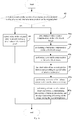
- the image processing method includes the followings.
- the image sensor is controlled to output a merged image.
- the merged image includes merged pixels arranged in a preset array.
- the photosensitive pixels in a same photosensitive pixel unit are collectively output as one merged pixel.
- the merged image has a first brightness.
- the image sensor is controlled to output a color-block image.
- the color-block image includes image pixel units arranged in the preset array. Each image pixel unit includes a plurality of original pixels, and each photosensitive pixel corresponds to one original pixel.
- the color-block image has a second brightness, and the first brightness is greater than the second brightness.
- the merged image is converted into a first image having the first brightness using a scaling algorithm.
- the first image having the first brightness includes first pixels arranged in the preset array, and each photosensitive pixel corresponds to one first pixel.
- the color-block image is converted into a second image having the second brightness using an interpolation algorithm.
- the second image having the second brightness includes second pixels arranged in the preset array, and each photosensitive pixel corresponds to one second pixel.
- the first image and the second image are merged to obtain a HDR image.
- the image sensor 200 can output images in two different modes (there is a brightness difference between the output images), a condition for applying the HDR mode is satisfied.
- directly performing HDR under the 16M mode that is, outputting a plurality of color-block images using different exposure values, performing the interpolation algorithm on each color-block image, and then merging them
- the processing time is reduced, and efficiency is improved.
- Fig. 4 is a schematic diagram illustrating a circuit of an image sensor according to an embodiment of the present disclosure.
- Fig. 5 is a schematic diagram of an array of filter units according to an embodiment of the present disclosure.
- Figs. 2-5 are better viewed together.
- the image sensor 200 according to an embodiment of the present disclosure includes an array 210 of photosensitive pixel units and an array 220 of filter units arranged on the array 210 of photosensitive pixel units.
- the array 210 of photosensitive pixel units includes a plurality of photosensitive pixel units 210a, and each photosensitive pixel unit 210a includes a plurality of adjacent photosensitive pixels 212.
- Each photosensitive pixel 212 includes a photosensitive element 2121 and a transmission tube 2122.
- the photosensitive element 2121 may be a photodiode
- the transmission tube 2122 may be a MOS transistor.
- the array 220 of filter units includes a plurality of filter units 220a. Each filter unit 220a corresponds to one photosensitive pixel unit 210a.
- the filter units 220a are arranged in a Bayer array.
- four adjacent filter units 220a include one red filter unit, one blue filter unit and two green filter units.
- Each photosensitive pixel unit 210a corresponds to a filter unit 220a with a same color. If a photosensitive pixel unit 210a includes n adjacent photosensitive elements 212, one filter unit 220a covers n photosensitive elements 212 in one photosensitive pixel unit 210a.
- the filter unit 220a may be formed integrally, or may be formed by assembling n separate sub filters.
- each photosensitive pixel unit 210a includes four adjacent photosensitive pixels 212. Two adjacent photosensitive pixels 212 collectively form one photosensitive pixel subunit 2120.
- the photosensitive pixel subunit 2120 further includes a source follower 2123 and an analog-to-digital converter 2124.
- the photosensitive pixel unit 210a further includes an adder 213.
- a first electrode of each transmission tube 2122 in the photosensitive pixel subunit 2120 is coupled to a cathode electrode of a corresponding photosensitive element 2121.
- Second electrodes of all the transmission tubes 2122 are collectively coupled to a gate electrode of the source follower 2123 and coupled to an analog-to-digital converter 2124 via the source electrode of the source follower 2123.
- the source follower 2123 may be a MOS transistor.
- Two photosensitive pixel subunits 2120 are coupled to the adder 213 via respective source followers 2123 and respective analog-to-digital converters 2124.
- four adjacent photosensitive elements 2121 in one photosensitive pixel unit 210a of the image sensor 200 collectively use one filter unit 220a with a same color as the photosensitive pixel unit.
- Each photosensitive element 2121 is coupled to a transmission tube 2122 correspondingly.
- Two adjacent photosensitive elements 2121 collectively use one source follower 2123 and one analog-digital converter 2124.
- Four adjacent photosensitive elements 2121 collectively use one adder 213.
- photosensitive elements 2121 are arranged in a 2-by-2 array.
- Two photosensitive elements 2121 in one photosensitive pixel subunit 2120 can be in a same row.
- pixels can be merged, and the merged image can be outputted.
- the photosensitive element 2121 is configured to convert light into charges, and the number of charges is proportional to an illumination intensity.
- the transmission tube 2122 is configured to control a circuit to turn on or off according to a control signal.
- the source follower 2123 is configured to convert the charge generated through light illumination into a voltage signal.
- the analog-to-digital converter 2124 is configured to convert the voltage signal into a digital signal.
- the adder 213 is configured to add and output two digital signals for processing by an image processing module connected to the image sensor 200.
- the image sensor 200 can merge photosensitive pixels of 16M into photosensitive pixels of 4M, i.e., the image sensor 200 outputs the merged image.
- the merged image includes merged pixels arranged in a preset array, and a plurality of photosensitive pixels 212 in a same photosensitive pixel unit 210a are merged and output as one merged pixel.
- each photosensitive pixel unit 210a includes four photosensitive pixels 212, that is, after the merging, the photosensitive pixel 212 quadruples in size, such that the photosensibility of the photosensitive pixel 212 is increased.
- noise points since most part of noise in the image sensor 200 is random, there may be noise points at one or two pixels. After four photosensitive pixels 212 are merged into a big photosensitive pixel 212, an effect of noise points on the big photosensitive pixel is reduced, i.e., the noise is weaken and SNR (signal to noise ratio) is improved.
- a color-block image can be output by image processing.
- the photosensitive element 2121 is configured to convert light into charges, and the number of charges is proportional to an illumination intensity.
- the transmission tube 2122 is configured to control a circuit to turn on or off according to a control signal.
- the source follower 2123 is configured to convert the charge generated through light illumination into a voltage signal.
- the analog-to-digital converter 2124 is configured to convert the voltage signal into a digital signal for processing by an image processing module connected to the image sensor 200.
- the image sensor 200 can output photosensitive pixels of 16M, i.e., the image sensor 200 outputs the color-block image.
- the color-block image includes image pixel units.
- the image pixel unit includes original pixels arranged in a 2-by-2 array. The size of the original pixel is the same as that of the photosensitive pixel.
- filter unit 220a covering four adjacent photosensitive elements 2121 has a same color (i.e., although four photosensitive elements 2121 are exposed respectively, the filter unit 220a covers the four photosensitive elements has a same color), four adjacent original pixels in each image pixel unit of the output image have a same color, and thus the resolution of the image cannot be increased and further processing is required.
- each photosensitive pixel is output separately. Since four adjacent photosensitive pixels have a same color, four adjacent original pixels in an image pixel unit have a same color, which form an untypical Bayer array. However, the untypical Bayer array cannot be directly processed.
- the image sensor 200 adopts a same image processing module for processing the image, in order to realize a compatibility of the true-color image outputs under two modes (i.e., the true-color image under a merged mode and the true-color image under a color-block mode), it is required to perform converting processing on the color-block image, or to convert the image pixel unit in an untypical Bayer array into pixels arranged in the typical Bayer array.
- a merged image when a merged image is output, four adjacent photosensitive pixels with the same color can be output as one merged pixel.
- the photosensibility or the brightness of the merged image is four times that of the color-block image.
- This brightness difference forms a condition for applying the HDR mode, that is, for a same object to be captured, a plurality of frames of image are output by using different exposure parameters and then merged. In this way, a HDR image processing can be directly performed by using the characteristic that images with different brightness can be output by the image sensor 200 in two output modes under a same exposure condition.
- the merged image is equivalent to outputting photosensitive pixels of 4M. Therefore, a size of the merged image output in this situation is different from that of the color-block image by outputting photosensitive pixels of 16M, and the size of the merged image can be processed before the merging.
- the merged image can be magnified with a scaling algorithm, such that the size of the merged image is made to be identical to that of the color-block image.
- the merged image is converted to a high brightness image (the first image having the first brightness).
- the high brightness image includes high brightness pixels (first pixels) arranged in a Bayer array.
- each photosensitive pixel unit in the color-block image is arranged in an untypical Bayer array, and thus the color-block image may not be directly processed to merge with the high brightness image (the first image having the first brightness).
- processing can be performed on the color-block image.
- the color-block image can be converted into a low brightness image (the second image having the second brightness) with an interpolation algorithm.
- the low brightness image includes low brightness pixels (second pixels) arranged in the preset array (i.e. a Bayer array). In this way, the high brightness image (the first image having the first brightness) and the low brightness image (the second image having the second brightness) can be merged, and then converted to a true-color image for display.
- parts with low brightness of the true-color image uses corresponding parts of the merged image, thus improving SNR of low brightness region
- parts with high brightness of the true-color image uses corresponding parts of the color-block image, thus improving resolution of high brightness region.
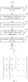
- the act at block 40 includes the followings.
- a pixel value of the original pixel is determined as a pixel value of the second pixel.
- the pixel value of the second pixel is determined according to a pixel value of an association pixel.
- the association pixel is selected from an image pixel unit with a same color as the second pixel and adjacent to an image pixel unit comprising the original pixel.
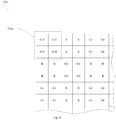
- the pixel value of the original pixel R33 is directly determined as the pixel value of the second pixel R3'3' during conversion.
- the pixel value of the original pixel B55 cannot be directly determined as the pixel value of the second pixel R5'5', and it is required to calculate the pixel value of the second pixel R5'5' according to an association pixel of the second pixel R5'5' by an interpolation algorithm.
- a pixel value of a pixel mentioned in the context should be understood in a broad sense as a color attribute value of the pixel, such as a color value.
- association pixel unit for each second pixel, for example, there may be four association pixel units, in which the association pixel units have the same color as the second pixel and are adjacent to the image pixel unit including the original pixel at the same position as the second pixel.
- the second pixel R5'5' corresponds to the original pixel B55.
- the image pixel units 400, 500, 600 and 700 are selected as the association pixel units, but other red image pixel units far away from the image pixel unit where the original pixel B55 is located are not selected as the association pixel units.
- the red original pixel closest to the original pixel B55 is selected as the association pixel, which means that the association pixels of the second pixel R5'5' include the original pixels R44, R74, R47 and R77.
- the second pixel R5'5' is adjacent to and has the same color as the original pixels R44, R74, R47 and R77.
- the original pixels can be converted into the second pixels in different ways, thus converting the color-block image into the second image having the second brightness. Since the filters in the Bayer array are adopted by the image sensor 200, the SNR of the image is improved. During the image processing procedure, the interpolation processing is performed on the color-block image by the interpolation algorithm, such that the distinguishability and resolution of the image can be improved.
- the act at block 46 i.e., determining the pixel value of the second pixel according to the pixel value of the association pixel
- the act at block 46 includes the followings.
- a change of the color of the second pixel in each direction of at least two directions is calculated according to the pixel value of the association pixel.
- a weight in each direction of the at least two directions is calculated according to the change.
- the pixel value of the second pixel is calculated according to the weight and the pixel value of the association pixel.
- the interpolation processing is realized as follows: with reference to energy changes of the image in different directions and according to weights of the association pixels in different directions, the pixel value of the second pixel is calculated by a linear interpolation. From the direction having a smaller energy change, it can get a higher reference value, i.e., the weight for this direction in the interpolation is high.
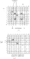
- the pixel value of the second pixel R5'5' is obtained by an interpolation based on the original pixels R44, R74, R47 and R77. Since there is no original pixel with a same color as the second pixel (i.e., R) in the horizontal direction and the vertical direction of the original pixel R55 corresponding the second pixel R5'5', a component of this color (i.e., R) in each of the horizontal direction and the vertical direction is calculated according to the association pixels.
- the components in the horizontal direction are R45 and R75, the components in the vertical direction are R54 and R57. All the components can be calculated according to the original pixels R44, R74, R47 and R77.
- R45 R44*2/3+R47*1/3
- R75 2/3*R74+1/3*R77
- R54 2/3*R44+1/3*R74
- R57 2/3*R47+1/3*R77.
- the change of color and the weight in each of the horizontal direction and the vertical direction are calculated respectively.
- the reference weight in each direction used in the interpolation is determined.
- the weight in the direction with a small change is high, while the weight in the direction with a big change is low.
- the pixel value of the second pixel can be calculated by the interpolation algorithm.
- the original pixels can be converted into the second pixels arranged in the typical Bayer array.
- four adjacent second pixels arranged in the 2-by-2 array include one red second pixel, two green second pixels and one blue second pixel.
- the interpolation processing is not limited to the above-mentioned method, in which only the pixel values of pixels with a same color as the second pixel in the vertical direction and the horizontal direction are considered during calculating the pixel value of the second pixel. In other embodiments, pixel values of pixels with other colors can also be considered.
- the method before the act at block 46, the method further includes performing a white-balance compensation on the color-block image, as illustrated at block 45a.
- the method further includes performing a reverse white-balance compensation on the simulation image, as illustrated at block 47a.
- the red and blue second pixels when converting the color-block image into the second image having the second brightness (the low brightness image), during the interpolation, not only refer to the color weights of original pixels having the same color as the second pixels, but also refer to the color weights of original pixels with the green color.
- it is required to perform the white-balance compensation before the interpolation to exclude an effect of the white-balance in the interpolation calculation.
- it is required to perform the reverse white-balance compensation after the interpolation according to gain values of the red, green and blue colors in the compensation.
- the effect of the white-balance in the interpolation calculation can be excluded, and the second image having the second brightness (the low brightness image) obtained after the interpolation can keep the white-balance of the color-block image.
- the method further includes performing a bad-point compensation on the color-block image, as illustrated at block 45b.
- the original pixels are detected.
- the bad-point compensation is performed according to pixel values of other original pixels in the image pixel unit where the original pixel is located.
- the method includes performing a crosstalk compensation on the color-block image, as illustrated at block 45c.
- photosensitive pixels in one photosensitive pixel unit cover the filters with the same color, and the photosensitive pixels have differences in photosensibility, such that fixed spectrum noise may occur in pure-color areas in the true-color image outputted after converting the second image having the second brightness, and the quality of the image may be affected. Therefore, it is required to perform the crosstalk compensation.
- the crosstalk compensation it is required to set the compensation parameters during the manufacturing process of the image sensor 200 of the imaging apparatus, and to store the parameters related to the crosstalk compensation into the storage of the imaging apparatus or the electronic device provided with the imaging apparatus, such as the mobile phone or tablet computer.
- the compensation parameters can be set by the followings.
- a preset luminous environment is provided.
- imaging parameters of the imaging apparatus are configured.
- multi-frame images are captured.
- the multi-frame images are processed to obtain crosstalk compensation parameters.
- the crosstalk compensation parameters are stored.
- the preset luminous environment may include an LED uniform plate having a color temperature of about 5000K and a brightness of about 1000 lux.
- the imaging parameters may include a gain value, a shutter value and a location of a lens. After setting the related parameters, the crosstalk compensation parameters can be obtained.
- multiple color-block images are obtained using the preset imaging parameters in the preset luminous environment, and combined into one combination color-block image, such that the effect of noise caused by using a single color-block image as reference can be reduced.
- the image pixel unit Gr includes original pixels Gr1, Gr2, Gr3 and Gr4.
- the purpose of the crosstalk compensation is to adjust the photosensitive pixels which may have different photosensibilities to have the same photosensibility.
- the average value is a reference value.
- a color-block image is obtained with the same luminous environment and same imaging parameters as the preset luminous environment and the preset imaging parameters, and the crosstalk compensation is performed on the color-block image according to the calculated compensation parameters to calculate compensated Gr'_avg, Gr'1/Gr'_avg, Gr'2/Gr'_avg, Gr'3/Gr'_avg and Gr'4/Gr'_avg.
- the accuracy of parameters can be determined according to the calculation results from a macro perspective and a micro perspective. From the micro perspective, when a certain original pixel after the compensation still has a big deviation which is easy to be sensed by the user after the imaging process, it means that the parameters are not accurate.
- a ratio threshold can be set for the micro perspective, and another ratio threshold and a number threshold can be set for the macro perspective. In this way, the verification can be performed on the crosstalk compensation parameters to ensure the accuracy of the compensation parameters and to reduce the effect of the crosstalk on the quality of the image.
- the method further includes performing at least one of a mirror shape correction, a demosaicking processing, a denoising processing and an edge sharpening processing on the image having the second brightness, as illustrated at block 47b.
- the second pixels are arranged in the typical Bayer array.
- the second image having the second brightness (low brightness image) can be processed, during which, the mirror shape correction, the demosaicking processing, the denoising processing and the edge sharpening processing are included, such that the processed image can be used to merge with the first image having the first brightness (high brightness image), thus obtaining the HDR image.
- the present disclosure also provides an image processing apparatus.
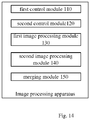
- Fig. 14 is a block diagram of an image processing apparatus according to an embodiment of the present disclosure.
- the image processing apparatu is applied in an electronic device.
- the electronic device includes an imaging apparatus.
- the imaging apparatus includes an image sensor 200.
- the image sensor 200 includes an array 210 of photosensitive pixel units and an array 220 of filter units arranged on the array 210 of photosensitive pixel units.
- Each filter unit 220a corresponds to one photosensitive pixel unit 210a, and each photosensitive pixel unit 210a includes a plurality of photosensitive pixels 212.
- the image processing apparatus includes a first control module 110, a second control module 120, a first image processing module 130, a second image processing module 140 and a merging module 150.
- the first control module 110 is configured to control the image sensor 200 to output a merged image.
- the merged image includes merged pixels arranged in a preset array, and the photosensitive pixels in a same photosensitive pixel unit are collectively output as one merged pixel.
- the merged image has a first brightness.
- the second control module 120 is configured to control the image sensor to output a color-block image.
- the color-block image includes image pixel units arranged in the preset array, each image pixel unit includes a plurality of original pixels, and each photosensitive pixel corresponds to one original pixel.
- the color-block image has a second brightness, and the first brightness is greater than the second brightness.
- the first image processing module 130 is configured to convert the merged image into a first image having the first brightness using a scaling algorithm.
- the first image having the first brightness includes first pixels arranged in the preset array, and each photosensitive pixel corresponds to one first pixel.
- the second image processing module 140 is configured to convert the color-block image into a second image having the second brightness using an interpolation algorithm.
- the second image having the second brightness includes second pixels arranged in the preset array, and each photosensitive pixel corresponds to one second pixel.
- the merging module is configured to merge the first image and the second image to obtain a HDR image.
- the image processing method according to embodiments of the present disclosure can be performed by the image processing apparatus according to embodiments of the present disclosure, which can be applied in the electronic device 1000, and configured to control the image sensor 200 of the imaging apparatus of the electronic device 1000 to output a HDR image.
- the image processing apparatus since the image sensor 200 can output images in two different modes (there is a brightness difference between the output images), a condition for applying the HDR mode is satisfied. Compared with directly performing HDR under the 16M mode (that is, outputting a plurality of color-block images using different exposure values, performing the interpolation algorithm on each color-block image, and then merging them), the processing time is reduced, and efficiency is improved.
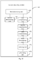
- the second converting module 140 includes a first determining unit 142, a second determining unit 144, and a third determining unit146.
- the first determining unit 142 is configured to determine whether a color of an original pixel is identical to that of a second pixel at a same position as the original pixel.
- the second determining unit 144 is configured to determine a pixel value of the original pixel as a pixel value of the second pixel when the color of the original pixel is identical to that of the second pixel at the same position as the original pixel.
- the third determining unit 146 is configured to determine the pixel value of the second pixel according to a pixel value of an association pixel when the color of the original pixel is different from that of the second pixel at the same position as the original pixel.
- the association pixel is selected from an image pixel unit with a same color as the second pixel and adjacent to an image pixel unit comprising the original pixel.
- the third determining unit 146 includes a first calculating subunit 1461, a second calculating subunit 1462, and a third calculating subunit 1463.
- the act at block 461 can be implemented by the first calculating subunit 1461.
- the first calculating subunit 1461 is configured to calculate a change of the color of the second pixel in each direction of at least two directions according to the pixel value of the association pixel.
- the second calculating subunit 1462 is configured to calculate a weight in each direction of the at least two directions according to the change.
- the third calculating subunit 1463 is configured to calculate the pixel value of the second pixel according to the weight and the pixel value of the association pixel.
- the second converting module 140 includes a first compensating unit 145a and a restoring unit 147a.
- the act at block 45a can be implemented by the first compensating unit 145a.
- the act at block 47a can be implemented by the restoring unit 147a.
- the first compensating unit 145a is configured to perform a white-balance compensation on the color-block image.
- the restoring unit 147a is configured to perform a reverse white-balance compensation on the image having the second brightness.
- the second converting module 140 further includes a second compensating unit 145b.
- the second compensating unit 145b is configured to perform a bad-point compensation on the color-block image.
- the second converting module 140 further includes a third compensating unit 145c.
- the third compensating unit 145c is configured to perform a crosstalk compensation on the color-block image.
- the second converting module 140 further includes a processing unit 147b.
- the processing unit 147b is configured to perform at least one of a mirror shape correction, a demosaicking processing, a denoising processing and an edge sharpening processing on the image having the second brightness.
- the present disclosure also provides an electronic device.
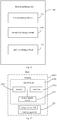
- Fig. 17 is a block diagram of an electronic device 1000 according to an embodiment of the present disclosure.
- the electronic device 1000 of the present disclosure includes a housing 1001, a processor 1002, a memory 1003, a circuit board 1006, a power supply circuit 1007 and an imaging apparatus 100.
- the circuit board 1006 is enclosed by the housing 1001.
- the processor 1002 and the memory 1003 are positioned on the circuit board 1006.
- the power supply circuit 1007 is configured to provide power for respective circuits or components of the electronic device 1000.
- the memory 1003 is configured to store executable program codes.
- the imaging apparatus 100 includes an image sensor 200. As illustrated above, the image sensor 200 includes an array 210 of photosensitive pixel units and an array 220 of filter units arranged on the array 210 of photosensitive pixel units. Each filter unit 220a corresponds to one photosensitive pixel unit 210a, and each photosensitive pixel unit 210a includes a plurality of photosensitive pixels 212.
- the processor 1002 is configured to run a program corresponding to the executable program codes by reading the executable program codes stored in the memory, to perform following operations: controlling an image sensor to output a merged image, in which, the merged image includes merged pixels arranged in a preset array, the photosensitive pixels in a same photosensitive pixel unit are collectively output as one merged pixel, and the merged image has a first brightness; controlling the image sensor to output a color-block image, in which, the color-block image includes image pixel units arranged in the preset array, each image pixel unit includes a plurality of original pixels, each photosensitive pixel corresponds to one original pixel, the color-block image has a second brightness, and the first brightness is greater than the second brightness; converting the merged image into a first image having the first brightness using a scaling algorithm, in which, the first image having the first brightness includes first pixels arranged in the preset array, and each photosensitive pixel corresponds to one first pixel; converting the color-block image into a second image
- the imaging apparatus includes a front camera or a real camera (not illustrated in Fig. 17 ).
- the processor 1002 is configured to run a program corresponding to the executable program codes by reading the executable program codes stored in the memory, to convert the color-block image into the second image by acts of: determining whether a color of an original pixel is identical to that of a second pixel at a same position as the original pixel; when the color of the original pixel is identical to that of the second pixel at the same position as the original pixel, determining a pixel value of the original pixel as a pixel value of the second pixel; and when the color of the original pixel is different from that of the second pixel at the same position as the original pixel, determining the pixel value of the second pixel according to a pixel value of an association pixel, in which the association pixel is selected from an image pixel unit with a same color as the second pixel and adjacent to an image pixel unit comprising the original pixel.
- the processor 1002 is configured to run a program corresponding to the executable program codes by reading the executable program codes stored in the memory, to determine the pixel value of the second pixel according to a pixel value of an association pixel by acts of: calculating a change of the color of the second pixel in each direction of at least two directions according to the pixel value of the association pixel; calculating a weight in each direction of the at least two directions according to the change; and calculating the pixel value of the second pixel according to the weight and the pixel value of the association pixel.
- the processor 1002 is configured to run a program corresponding to the executable program codes by reading the executable program codes stored in the memory, to perform following operations: performing a white-balance compensation on the color-block image; and performing a reverse white-balance compensation on the image having the second brightness.
- the processor 1002 is configured to run a program corresponding to the executable program codes by reading the executable program codes stored in the memory, to perform following operation: performing at least one of a bad-point compensation and a crosstalk compensation on the color-block image.
- the processor 1002 is configured to run a program corresponding to the executable program codes by reading the executable program codes stored in the memory, to perform following operations: performing at least one of a mirror shape correction, a demosaicking processing, a denoising processing and an edge sharpening processing on the image having the second brightness.
- the electronic device 1000 may be a mobile phone or a tablet computer, which is not limited herein.
- the electronic device 1000 may further include an inputting component (not illustrated in Fig. 17 ). It should be understood that, the inputting component may further include one or more of the followings: an inputting interface, a physical button of the electronic device 1000, a microphone, etc.
- the electronic device 1000 may further include one or more of the following components (not illustrated in Fig. 17 ): an audio component, an input/output (I/O) interface, a sensor component and a communication component.
- the audio component is configured to output and/or input audio signals, for example, the audio component includes a microphone.
- the I/O interface is configured to provide an interface between the processor 1002 and peripheral interface modules.
- the sensor component includes one or more sensors to provide status assessments of various aspects of the electronic device 1000.
- the communication component is configured to facilitate communication, wired or wirelessly, between the electronic device 1000 and other devices.
- phraseology and terminology used herein with reference to device or element orientation are only used to simplify description of the present invention, and do not indicate or imply that the device or element referred to must have or operated in a particular orientation. They cannot be seen as limits to the present disclosure.
- first and second are only used for description and cannot be seen as indicating or implying relative importance or indicating or implying the number of the indicated technical features. Thus, the features defined with “first” and “second” may comprise or imply at least one of these features. In the description of the present disclosure, "a plurality of' means two or more than two, unless specified otherwise.
- the terms “mounted,” “connected,” “coupled,” “fixed” and the like are used broadly, and may be, for example, fixed connections, detachable connections, or integral connections; may also be mechanical or electrical connections; may also be direct connections or indirect connections via intervening structures; may also be inner communications of two elements or interactions of two elements, which can be understood by those skilled in the art according to specific situations.
- a structure in which a first feature is "on" a second feature may include an embodiment in which the first feature directly contacts the second feature, and may also include an embodiment in which the first feature indirectly contacts the second feature via an intermediate medium.
- a structure in which a first feature is "on”, “over” or “above” a second feature may indicate that the first feature is right above the second feature or obliquely above the second feature, or just indicate that a horizontal level of the first feature is higher than the second feature.
- a structure in which a first feature is "below”, or “under” a second feature may indicate that the first feature is right under the second feature or obliquely under the second feature, or just indicate that a horizontal level of the first feature is lower than the second feature.
- Any process or method described in a flow chart or described herein in other ways may be understood to include one or more modules, segments or portions of codes of executable instructions for achieving specific logical functions or steps in the process, and the scope of a preferred embodiment of the present disclosure includes other implementations, wherein the order of execution may differ from that which is depicted or discussed, including according to involved function, executing concurrently or with partial concurrence or in the contrary order to perform the function, which should be understood by those skilled in the art.
- the logic and/or step described in other manners herein or shown in the flow chart, for example, a particular sequence table of executable instructions for realizing the logical function may be specifically achieved in any computer readable medium to be used by the instruction execution system, device or equipment (such as the system based on computers, the system comprising processors or other systems capable of acquiring the instruction from the instruction execution system, device and equipment and executing the instruction), or to be used in combination with the instruction execution system, device and equipment.
- the computer readable medium may be any device adaptive for including, storing, communicating, propagating or transferring programs to be used by or in combination with the instruction execution system, device or equipment.
- the computer-readable medium comprise but are not limited to: an electronic connection (an electronic device) with one or more wires, a portable computer enclosure (a magnetic device), a random access memory (RAM), a read-only memory (ROM), an erasable programmable read-only memory (EPROM or a flash memory), an optical fiber device and a portable compact disk read-only memory (CDROM).
- the computer-readable medium may even be a paper or other appropriate medium capable of printing programs thereon, this is because, for example, the paper or other appropriate medium may be optically scanned and then edited, decrypted or processed with other appropriate methods when necessary to obtain the programs in an electric manner, and then the programs may be stored in the computer memories.
- each part of the present disclosure may be realized by hardware, software, firmware or their combination.
- a plurality of steps or methods may be realized by the software or firmware stored in the memory and executed by the appropriate instruction execution system.
- the steps or methods may be realized by one or a combination of the following techniques known in the art: a discrete logic circuit having a logic gate circuit for realizing a logic function of a data signal, an application-specific integrated circuit having an appropriate combination logic gate circuit, a programmable gate array (PGA), a field programmable gate array (FPGA), etc..
- each function cell of the embodiments of the present disclosure may be integrated in a processing module, or these cells may be separate physical existence, or two or more cells are integrated in a processing module.
- the integrated module may be realized in a form of hardware or in a form of software function modules. When the integrated module is realized in a form of software function module and is sold or used as a standalone product, the integrated module may be stored in a computer-readable storage medium.
- the storage medium mentioned above may be read-only memories, magnetic disks, CD, etc.
Landscapes
- Engineering & Computer Science (AREA)
- Multimedia (AREA)
- Signal Processing (AREA)
- Physics & Mathematics (AREA)
- Spectroscopy & Molecular Physics (AREA)
- General Physics & Mathematics (AREA)
- Theoretical Computer Science (AREA)
- Color Television Image Signal Generators (AREA)
Claims (13)
- Bildverarbeitungsverfahren für eine elektronische Vorrichtung, wobei die elektronische Vorrichtung eine Abbildungsvorrichtung umfasst, die einen Bildsensor (200) umfasst, wobei der Bildsensor (200) eine Anordnung (210) photoempfindlicher Pixeleinheiten (210a) und eine Anordnung (220) von Filtereinheiten (220a) umfasst, die auf der Anordnung (210) photoempfindlicher Pixeleinheiten angeordnet sind (210a), jede Filtereinheit (220a) entspricht einer photoempfindlichen Pixeleinheit (210a) und umfasst eine Vielzahl von Filtern in der gleichen Farbe, wobei jede photoempfindliche Pixeleinheit (210a) eine Vielzahl von photoempfindlichen Pixeln umfasst (212), die nebeneinander liegen, und jedes photoempfindliche Pixel (212) einer photoempfindlichen Pixeleinheit von einem Filter abgedeckt ist, wobei das Bildverarbeitungsverfahren Folgendes umfasst:Kontrollieren (10) des Bildsensors (200) auf die Ausgabe eines verschmolzenen Bildes, wobei das verschmolzene Bild in einer Bayer-Anordnung angeordnete verschmolzene Pixel umfasst, die in derselben photoempfindlichen Pixeleinheit (210a) nebeneinander angeordneten photoempfindlichen Pixel (212) zusammen als eine verschmolzene Pixeleinheit ausgegeben werden, und wobei das verschmolzene Bild eine erste Helligkeit aufweist;Kontrollieren (20) des Bildsensors auf die Ausgabe eines Farbblockbildes, wobei das Farbblockbild in einer vorgegebenen Anordnung angeordnete Pixeleinheiten umfasst, wobei die vorgegebene Anordnung die Bayer-Anordnung umfasst, jede Pixeleinheit eine Vielzahl von ursprünglichen Pixeln, die nebeneinander angeordnet sind, umfasst, jedes photoempfindliche Pixel einem ursprünglichen Pixel entspricht, das Farbblockbild eine zweite Helligkeit aufweist, und die erste Helligkeit heller ist als die zweite Helligkeit;Umwandeln (30) des verschmolzenen Bildes in ein erstes Bild mit der ersten Helligkeit mittels eines Skalierungsalgorithmus, wobei das erste Bild erste, in der Bayer-Anordnung angeordnete Pixel, umfasst, und jedes photoempfindliche Pixel (212) einem ersten Pixel entspricht;Umwandeln (40) des Farbblockbildes in ein zweites Bild mit der zweiten Helligkeit mittels eines Interpolationsalgorithmus, wobei das zweite Bild zweite, in der Bayer-Anordnung angeordnete Pixel, umfasst, und jedes photoempfindliche Pixel (212) einem zweiten Pixel entsprichtZusammenführen (50) des ersten und des zweiten Bildes, um ein High Dynamic Range (HDR)-Bild zu erhalten;Durchführen einer Weißabgleich-Kompensation (45a) bei dem Farbblockbild; undDurchführen einer umgekehrten Weißabgleich-Kompensation (47a) bei dem zweiten Bild.
- Bildverarbeitungsverfahren nach Anspruch 1, wobei das Umwandeln (40) des Farbblockbildes in ein zweites Bild mittels des Interpolationsalgorithmus Folgendes umfasst:Bestimmen (42), ob eine Farbe eines ursprünglichen Pixels mit der eines zweiten Pixels in derselben Position wie das ursprüngliche Pixel übereinstimmt;Bestimmen (44) eines Pixelwertes des ursprünglichen Pixels als einen Pixelwert des zweiten Pixels, wenn die Farbe des ursprünglichen Pixels mit der des zweiten Pixels in derselben Position wie das ursprüngliche Pixel übereinstimmt; undBestimmen (46) des Pixelwertes des zweiten Pixels entsprechend eines Pixelwertes eines Assoziationspixels, wobei das Assoziationspixel aus einer Bildpixeleinheit, die dieselbe Farbe wie das zweite Pixel hat und neben einer Bildpixeleinheit liegt, die das ursprüngliche Pixel umfasst, ausgewählt wird, wenn die Farbe des ursprünglichen Pixels sich von der des zweiten Pixels in derselben Position wie das ursprüngliche Pixel unterscheidet.
- Bildverarbeitungsverfahren nach Anspruch 2, wobei das Bestimmen (46) des Pixelwertes des zweiten Pixels entsprechend eines Pixelwertes eines Assoziationspixels das Folgende umfasst:Berechnen (461) einer Farbänderung des zweiten Pixels in jede Richtung von mindestens zwei Richtungen entsprechend des Pixelwertes des Assoziationspixels;Berechnen (462) eines Gewichts in jede Richtung von mindestens zwei Richtungen entsprechend der Änderung; undBerechnen (463) des Pixelwerts des zweiten Pixels entsprechend des Gewichts und des Pixelwertes des Assoziationspixels.
- Bildverarbeitungsverfahren nach einem der Ansprüche 1-3, wobei die Bildpixeleinheit ursprüngliche Pixel, die in einer 2 x 2-Anordnung angeordnet sind, umfasst.
- Bildverarbeitungsverfahren nach einem der Ansprüche 1-4, das weiterhin mindestens eins des Folgenden umfasst:Durchführen mindestens einer Fehlerkompensation (45b) und einer Übersprechkompensation (45c) bei dem Farbblockbild; undDurchführen mindestens eines Rauschunterdrückungsverfahrens und eines Kantenschärfungsverfahrens (47b) bei dem zweiten Bild.
- Bildverarbeitungsverfahren nach einem der Ansprüche 1-5, wobei die zweite Helligkeit einer Hälfte oder einem Viertel der ersten Helligkeit entspricht.
- Bildverarbeitungsvorrichtung, die für das Anwenden in einer elektronischen Vorrichtung geeignet ist, wobei die elektronische Vorrichtung eine Abbildungsvorrichtung umfasst, die einen Bildsensor (200) umfasst, wobei der Bildsensor (200) eine Anordnung (210) von photoempfindlichen Pixeleinheiten (210a) und eine Anordnung (220) von Filtereinheiten (220a), die auf der Anordnung (210) von photoempfindlichen Pixeleinheiten(210a) angeordnet sind, umfasst, wobei jede Filtereinheit (220a) einer photoempfindlichen Pixeleinheit(210a) entspricht und eine Vielzahl von Filtern derselben Farbe umfasst, wobei jede photoempfindliche Pixeleinheit (210a) eine Vielzahl von photoempfindlichen Pixeln (212) umfasst, die nebeneinander liegen, und jedes photoempfindliche Pixel (212) einer photoempfindlichen Pixeleinheit von einem Filter abgedeckt ist; die Bildverarbeitungsvorrichtung umfasst:ein erstes Kontrollmodul (110), das dazu konfiguriert ist, die Ausgabe eines verschmolzenen Bildes durch den Bildsensor (200) zu kontrollieren, wobei das verschmolzene Bild verschmolzene Pixel umfasst, die in einer Bayer-Anordnung angeordnet sind, die photoempfindlichen Pixel (212), die nebeneinander in derselben photoempfindlichen Pixeleinheit (210a) angeordnet sind, werden zusammen als ein verschmolzenes Bild ausgegeben und das verschmolzene Bild hat eine erste Helligkeit;ein zweites Kontrollmodul (120), das dazu konfiguriert ist, die Ausgabe eines Farbblockbildes durch den Bildsensor (200) zu kontrollieren, wobei das Farbblockbild Pixel, die in einer vorgegebenen Anordnung angeordnet sind, umfasst, wobei die vorgegebene Anordnung die Bayer-Anordnung umfasst, jede Pixeleinheit eine Vielzahl von nebeneinander angeordneten ursprünglichen Pixeln umfasst, jedes photoempfindliche Pixel (212) einem ursprünglichen Pixel entspricht, das Farbblockbild eine zweite Helligkeit aufweist und die erste Helligkeit größer ist als die zweite Helligkeit;ein erstes Bildverarbeitungsmodul (130), das dazu konfiguriert ist, das verschmolzene Bild in ein erstes Bild mit der ersten Helligkeit mittels eines Skalierungsalgorithmus umzuwandeln, wobei das erste Bild erste Pixel umfasst, die in einer Bayer-Anordnung angeordnet sind, und jedes photoempfindliche Pixel einem ersten Pixel entspricht;ein zweites Bildverarbeitungsmodul (140), das dazu konfiguriert ist, das Farbblockbild in ein zweites Bild mit der zweiten Helligkeit mittels eines Interpolationsalgorithmus umzuwandeln, wobei das zweite Bild zweite Pixel umfasst, die in der Bayer-Anordnung angeordnet sind und jedes photoempfindliche Pixel (212) einem zweiten Pixel entspricht; undein Verschmelzungsmodul (150), das dazu konfiguriert ist, das erste Bild und das zweite Bild für das Erhalten eines High Dynamic Range (HDR)-Bildes zu verschmelzen;wobei das zweite Umwandlungsmodul (140) Folgendes umfasst:eine erste Kompensationseinheit (145a), die dazu konfiguriert ist, einen Weißabgleich bei dem Farbblockbild durchzuführen; undeine Rückstelleinheit (147a), die dazu konfiguriert ist, einen umgekehrten Weißabgleich bei dem zweiten Bild durchzuführen.
- Bildverarbeitungsvorrichtung nach Anspruch 7, wobei das zweite Bildverarbeitungsmodul (140) Folgendes umfasst:eine erste Bestimmungseinheit (142), die dazu konfiguriert ist, zu bestimmen, ob eine Farbe eines ursprünglichen Pixels identisch mit der eines zweiten Pixels in derselben Position wie das ursprüngliche Pixel ist;eine zweite Bestimmungseinheit (144), die dazu konfiguriert ist, einen Pixelwert des ursprünglichen Pixels als einen Pixelwert des zweiten Pixels zu bestimmen, wenn die Farbe des ursprünglichen Pixels mit der des zweiten Pixels in derselben Position wie das ursprüngliche Pixel identisch ist; undeine dritte Bestimmungseinheit (146), die dazu konfiguriert ist, den Pixelwert des zweiten Pixels entsprechend eines Pixelwertes eines Assoziationspixels zu bestimmen, wenn die Farbe des ursprünglichen Pixels sich von der des zweiten Pixels in derselben Position wie das ursprüngliche Pixel unterscheidet, wobei das Assoziationspixel aus einer Bildpixeleinheit mit derselben Farbe wie das zweite Pixel ausgewählt wird und neben einer Bildpixeleinheit liegt, die das ursprüngliche Pixel umfasst.
- Bildverarbeitungsvorrichtung nach Anspruch 8, wobei die dritte Bestimmungseinheit (146) Folgendes umfasst:eine erste Berechnungsuntereinheit (1461), die dazu konfiguriert ist, eine Farbänderung des zweiten Pixels in jede Richtung von mindestens zwei Richtungen entsprechend des Pixelwertes des Assoziationspixels zu berechnen;eine zweite Berechnungsuntereinheit (1462), die dazu konfiguriert ist, ein Gewicht in jede Richtung von den mindestens zwei Richtungen entsprechend der Änderung zu berechnen; undeine dritte Berechnungsuntereinheit (1463), die dazu konfiguriert ist, den Pixelwert des zweiten Pixels entsprechend des Gewichts und des Pixelwerts des Assoziationspixels zu berechnen.
- Bildverarbeitungsvorrichtung nach einem der Ansprüche 7-9, wobei die Bildpixeleinheit ursprüngliche Pixel, die in einer 2 x 2-Anordnung angeordnet sind, umfasst.
- Bildverarbeitungsvorrichtung nach einem der Ansprüche 7-10, wobei das zweite Umwandlungsmodul (140) mindestens eine von einer zweiten Kompensationseinheit (145b), einer dritten Kompensationseinheit (145c) und einer Verarbeitungseinheit (147b) umfasst; wobei
die zweite Kompensationseinheit (145b) dazu konfiguriert ist, eine Fehlerkompensation bei dem Farbblockbild durchzuführen;
die dritte Kompensationseinheit (145c) dazu konfiguriert ist, eine Übersprechkompensation bei dem Farbblockbild durchzuführen; und
die Verarbeitungseinheit (147b) dazu konfiguriert ist, mindestens eins von einem Rauschunterdrückungsverfahren und einem Kantenschärfungsverfahren bei dem zweiten Bild durchzuführen. - Bildverarbeitungsvorrichtung nach einem der Ansprüche 7-11, wobei die zweite Helligkeit einer Hälfte oder einem Viertel der ersten Helligkeit entspricht.
- Elektronische Vorrichtung (1000), die ein Gehäuse (1001), einen Prozessor (1002), einen Speicher (1003), eine Leiterplatte (1006), eine Stromversorgungsschaltung (1007) und eine Abbildungsvorrichtung (100) umfasst, wobei
die Leiterplatte (1006) von dem Gehäuse (1001) eingeschlossen ist;
der Prozessor (1002) und der Speicher (1003) auf der Leiterplatte (1006) positioniert sind;
die Stromversorgungsschaltung (1007) dazu konfiguriert ist, Strom für die jeweiligen Schaltungen oder Komponenten der elektronischen Vorrichtung (1000) zu liefern;
die Bildvorrichtung (100) einen Bildsensor (200) umfasst, wobei der Bildsensor (200) eine Anordnung (210) von photoempfindlichen Pixeleinheiten (210a) und eine Anordnung (220) von Filtereinheiten, die auf der Anordnung von photoempfindlichen Pixeleinheiten (220a) angeordnet sind, umfasst, jede Filtereinheit (220a) einer photoempfindlichen Pixeleinheit (210a) entspricht und eine Vielzahl von gleichfarbigen Filtern umfasst, jede photoempfindliche Pixeleinheit (210a) eine Vielzahl von nebeneinander liegenden photoempfindlichen Pixeln (212) umfasst und jedes photoempfindliche Pixel (212) einer photoempfindlichen Pixeleinheit von einem Filter abgedeckt ist;
der Speicher (1003) dazu konfiguriert ist, ausführbare Programmcodes zu speichern; und
der Prozessor (1002) dazu konfiguriert ist, ein Programm, das den ausführbaren Programmcodes entspricht, durch Lesen der auf dem Speicher (1002) gespeicherten ausführbaren Programmcodes auszuführen, um das Bildverarbeitungsverfahren nach den Ansprüchen 1-6 durchzuführen.
Applications Claiming Priority (1)
| Application Number | Priority Date | Filing Date | Title |
|---|---|---|---|
| CN201611079317.4A CN106412407B (zh) | 2016-11-29 | 2016-11-29 | 控制方法、控制装置及电子装置 |
Publications (2)
| Publication Number | Publication Date |
|---|---|
| EP3328077A1 EP3328077A1 (de) | 2018-05-30 |
| EP3328077B1 true EP3328077B1 (de) | 2020-01-01 |
Family
ID=58085618
Family Applications (1)
| Application Number | Title | Priority Date | Filing Date |
|---|---|---|---|
| EP17199851.1A Active EP3328077B1 (de) | 2016-11-29 | 2017-11-03 | Bildverarbeitungsverfahren und -vorrichtung sowie elektronische vorrichtung |
Country Status (5)
| Country | Link |
|---|---|
| US (1) | US10531019B2 (de) |
| EP (1) | EP3328077B1 (de) |
| CN (1) | CN106412407B (de) |
| ES (1) | ES2769306T3 (de) |
| WO (1) | WO2018099010A1 (de) |
Cited By (1)
| Publication number | Priority date | Publication date | Assignee | Title |
|---|---|---|---|---|
| CN111355937A (zh) * | 2020-03-11 | 2020-06-30 | 北京迈格威科技有限公司 | 图像处理方法、装置和电子设备 |
Families Citing this family (20)
| Publication number | Priority date | Publication date | Assignee | Title |
|---|---|---|---|---|
| CN106791477B (zh) | 2016-11-29 | 2019-07-19 | Oppo广东移动通信有限公司 | 图像处理方法、图像处理装置、成像装置及制造方法 |
| CN106412407B (zh) * | 2016-11-29 | 2019-06-07 | Oppo广东移动通信有限公司 | 控制方法、控制装置及电子装置 |
| CN107222681B (zh) * | 2017-06-30 | 2018-11-30 | 维沃移动通信有限公司 | 一种图像数据的处理方法和移动终端 |
| CN108270942B (zh) * | 2018-01-31 | 2020-09-25 | 威海华菱光电股份有限公司 | 图像扫描装置、控制图像扫描光信号的接收方法及装置 |
| CN108419022A (zh) * | 2018-03-06 | 2018-08-17 | 广东欧珀移动通信有限公司 | 控制方法、控制装置、计算机可读存储介质和计算机设备 |
| CN110876014B (zh) * | 2018-08-31 | 2022-04-08 | 北京小米移动软件有限公司 | 图像处理方法及装置、电子设备及存储介质 |
| CN110874829B (zh) * | 2018-08-31 | 2022-10-14 | 北京小米移动软件有限公司 | 图像处理方法及装置、电子设备及存储介质 |
| CN111835941B (zh) * | 2019-04-18 | 2022-02-15 | 北京小米移动软件有限公司 | 图像生成方法及装置、电子设备、计算机可读存储介质 |
| US11570424B2 (en) | 2019-06-24 | 2023-01-31 | Infineon Technologies Ag | Time-of-flight image sensor resolution enhancement and increased data robustness using a binning module |
| CN110675404B (zh) * | 2019-09-03 | 2023-03-21 | RealMe重庆移动通信有限公司 | 图像处理方法、图像处理装置、存储介质与终端设备 |
| CN110519485B (zh) * | 2019-09-09 | 2021-08-31 | Oppo广东移动通信有限公司 | 图像处理方法、装置、存储介质及电子设备 |
| KR102625261B1 (ko) | 2019-10-21 | 2024-01-12 | 삼성전자주식회사 | 이미지 장치 |
| CN112785533B (zh) * | 2019-11-07 | 2023-06-16 | RealMe重庆移动通信有限公司 | 图像融合方法、图像融合装置、电子设备与存储介质 |
| KR102880112B1 (ko) * | 2020-03-04 | 2025-11-03 | 에스케이하이닉스 주식회사 | 이미지 센싱 장치 및 그의 동작 방법 |
| CN111491111B (zh) * | 2020-04-20 | 2021-03-26 | Oppo广东移动通信有限公司 | 高动态范围图像处理系统及方法、电子设备和可读存储介质 |
| CN111970451B (zh) * | 2020-08-31 | 2022-01-07 | Oppo(重庆)智能科技有限公司 | 图像处理方法、图像处理装置及终端设备 |
| CN112492161B (zh) * | 2020-11-30 | 2021-10-26 | 维沃移动通信有限公司 | 图像传感器、摄像模组和电子设备 |
| CN112492162B (zh) * | 2020-11-30 | 2022-04-01 | 维沃移动通信有限公司 | 图像传感器、摄像模组和电子设备 |
| CN112437237B (zh) * | 2020-12-16 | 2023-02-03 | 维沃移动通信有限公司 | 拍摄方法及装置 |
| KR20220135801A (ko) * | 2021-03-31 | 2022-10-07 | 에스케이하이닉스 주식회사 | 컬러 보정 회로, 이미징 센싱 장치 및 그 동작방법 |
Family Cites Families (17)
| Publication number | Priority date | Publication date | Assignee | Title |
|---|---|---|---|---|
| KR100843087B1 (ko) * | 2006-09-06 | 2008-07-02 | 삼성전자주식회사 | 영상 생성 장치 및 방법 |
| US8102435B2 (en) * | 2007-09-18 | 2012-01-24 | Stmicroelectronics S.R.L. | Method for acquiring a digital image with a large dynamic range with a sensor of lesser dynamic range |
| US7777804B2 (en) * | 2007-10-26 | 2010-08-17 | Omnivision Technologies, Inc. | High dynamic range sensor with reduced line memory for color interpolation |
| US7745779B2 (en) * | 2008-02-08 | 2010-06-29 | Aptina Imaging Corporation | Color pixel arrays having common color filters for multiple adjacent pixels for use in CMOS imagers |
| TWI422020B (zh) | 2008-12-08 | 2014-01-01 | Sony Corp | 固態成像裝置 |
| US8462221B2 (en) * | 2010-11-03 | 2013-06-11 | Eastman Kodak Company | Method for producing high dynamic range images |
| US8456557B2 (en) * | 2011-01-31 | 2013-06-04 | SK Hynix Inc. | Dynamic range extension for CMOS image sensors for mobile applications |
| JP2013038504A (ja) * | 2011-08-04 | 2013-02-21 | Sony Corp | 撮像装置、および画像処理方法、並びにプログラム |
| JP2013066140A (ja) * | 2011-08-31 | 2013-04-11 | Sony Corp | 撮像装置、および信号処理方法、並びにプログラム |
| JP2013066146A (ja) * | 2011-08-31 | 2013-04-11 | Sony Corp | 画像処理装置、および画像処理方法、並びにプログラム |
| CN104170376B (zh) * | 2012-03-27 | 2016-10-19 | 索尼公司 | 图像处理设备、成像装置及图像处理方法 |
| CN103531603B (zh) * | 2013-10-30 | 2018-10-16 | 上海集成电路研发中心有限公司 | 一种cmos图像传感器 |
| US9479695B2 (en) * | 2014-07-31 | 2016-10-25 | Apple Inc. | Generating a high dynamic range image using a temporal filter |
| CN105472266A (zh) * | 2015-12-18 | 2016-04-06 | 广东欧珀移动通信有限公司 | 高动态范围图像的生成方法、拍照装置和终端 |
| CN105578005B (zh) * | 2015-12-18 | 2018-01-19 | 广东欧珀移动通信有限公司 | 图像传感器的成像方法、成像装置和电子装置 |
| CN105592270B (zh) * | 2015-12-18 | 2018-02-06 | 广东欧珀移动通信有限公司 | 图像亮度补偿方法、装置及终端设备 |
| CN106412407B (zh) * | 2016-11-29 | 2019-06-07 | Oppo广东移动通信有限公司 | 控制方法、控制装置及电子装置 |
-
2016
- 2016-11-29 CN CN201611079317.4A patent/CN106412407B/zh not_active Expired - Fee Related
-
2017
- 2017-05-19 WO PCT/CN2017/085214 patent/WO2018099010A1/zh not_active Ceased
- 2017-10-13 US US15/783,150 patent/US10531019B2/en active Active
- 2017-11-03 ES ES17199851T patent/ES2769306T3/es active Active
- 2017-11-03 EP EP17199851.1A patent/EP3328077B1/de active Active
Non-Patent Citations (1)
| Title |
|---|
| None * |
Cited By (2)
| Publication number | Priority date | Publication date | Assignee | Title |
|---|---|---|---|---|
| CN111355937A (zh) * | 2020-03-11 | 2020-06-30 | 北京迈格威科技有限公司 | 图像处理方法、装置和电子设备 |
| CN111355937B (zh) * | 2020-03-11 | 2021-11-16 | 北京迈格威科技有限公司 | 图像处理方法、装置和电子设备 |
Also Published As
| Publication number | Publication date |
|---|---|
| US20180152646A1 (en) | 2018-05-31 |
| WO2018099010A1 (zh) | 2018-06-07 |
| EP3328077A1 (de) | 2018-05-30 |
| ES2769306T3 (es) | 2020-06-25 |
| CN106412407A (zh) | 2017-02-15 |
| CN106412407B (zh) | 2019-06-07 |
| US10531019B2 (en) | 2020-01-07 |
Similar Documents
| Publication | Publication Date | Title |
|---|---|---|
| US10531019B2 (en) | Image processing method and apparatus, and electronic device | |
| EP3327781B1 (de) | Bildverarbeitungsverfahren und -vorrichtung sowie elektronische vorrichtung | |
| US10559070B2 (en) | Image processing method and apparatus, and electronic device | |
| EP3328071B1 (de) | Bildverarbeitungsverfahren und -vorrichtung sowie elektronische vorrichtung | |
| EP3327779B1 (de) | Bildverarbeitungsverfahren und -vorrichtung sowie elektronische vorrichtung | |
| US10339632B2 (en) | Image processing method and apparatus, and electronic device | |
| EP3328075B1 (de) | Bildverarbeitungsverfahren und -vorrichtung sowie elektronische vorrichtung | |
| EP3328078B1 (de) | Bildverarbeitungsverfahren und -vorrichtung sowie elektronische vorrichtung | |
| US10382709B2 (en) | Image processing method and apparatus, and electronic device | |
| US20180247391A1 (en) | Image processing method and apparatus, and electronic device | |
| US10262395B2 (en) | Image processing method and apparatus, and electronic device | |
| EP3327664A1 (de) | Bildverarbeitungsverfahren und -vorrichtung, elektronische vorrichtung und steuerungsverfahren | |
| EP3327665A1 (de) | Bildverarbeitungsverfahren und -vorrichtung sowie elektronische vorrichtung | |
| CN106791477A (zh) | 图像处理方法、图像处理装置、成像装置及制造方法 |
Legal Events
| Date | Code | Title | Description |
|---|---|---|---|
| PUAI | Public reference made under article 153(3) epc to a published international application that has entered the european phase |
Free format text: ORIGINAL CODE: 0009012 |
|
| STAA | Information on the status of an ep patent application or granted ep patent |
Free format text: STATUS: REQUEST FOR EXAMINATION WAS MADE |
|
| 17P | Request for examination filed |
Effective date: 20171103 |
|
| AK | Designated contracting states |
Kind code of ref document: A1 Designated state(s): AL AT BE BG CH CY CZ DE DK EE ES FI FR GB GR HR HU IE IS IT LI LT LU LV MC MK MT NL NO PL PT RO RS SE SI SK SM TR |
|
| AX | Request for extension of the european patent |
Extension state: BA ME |
|
| STAA | Information on the status of an ep patent application or granted ep patent |
Free format text: STATUS: EXAMINATION IS IN PROGRESS |
|
| 17Q | First examination report despatched |
Effective date: 20190114 |
|
| REG | Reference to a national code |
Ref country code: DE Ref legal event code: R079 Ref document number: 602017010345 Country of ref document: DE Free format text: PREVIOUS MAIN CLASS: H04N0009070000 Ipc: H04N0005347000 |
|
| GRAP | Despatch of communication of intention to grant a patent |
Free format text: ORIGINAL CODE: EPIDOSNIGR1 |
|
| STAA | Information on the status of an ep patent application or granted ep patent |
Free format text: STATUS: GRANT OF PATENT IS INTENDED |
|
| RIC1 | Information provided on ipc code assigned before grant |
Ipc: H04N 5/235 20060101ALI20190708BHEP Ipc: G06T 5/50 20060101ALI20190708BHEP Ipc: H04N 5/355 20110101ALI20190708BHEP Ipc: H04N 9/73 20060101ALI20190708BHEP Ipc: H04N 9/04 20060101ALI20190708BHEP Ipc: H04N 5/347 20110101AFI20190708BHEP Ipc: G06T 3/40 20060101ALI20190708BHEP |
|
| INTG | Intention to grant announced |
Effective date: 20190729 |
|
| GRAS | Grant fee paid |
Free format text: ORIGINAL CODE: EPIDOSNIGR3 |
|
| GRAA | (expected) grant |
Free format text: ORIGINAL CODE: 0009210 |
|
| STAA | Information on the status of an ep patent application or granted ep patent |
Free format text: STATUS: THE PATENT HAS BEEN GRANTED |
|
| RAP1 | Party data changed (applicant data changed or rights of an application transferred) |
Owner name: GUANGDONG OPPO MOBILE TELECOMMUNICATIONS CORP., LT |
|
| AK | Designated contracting states |
Kind code of ref document: B1 Designated state(s): AL AT BE BG CH CY CZ DE DK EE ES FI FR GB GR HR HU IE IS IT LI LT LU LV MC MK MT NL NO PL PT RO RS SE SI SK SM TR |
|
| REG | Reference to a national code |
Ref country code: GB Ref legal event code: FG4D |
|
| REG | Reference to a national code |
Ref country code: CH Ref legal event code: EP Ref country code: AT Ref legal event code: REF Ref document number: 1221296 Country of ref document: AT Kind code of ref document: T Effective date: 20200115 |
|
| REG | Reference to a national code |
Ref country code: DE Ref legal event code: R096 Ref document number: 602017010345 Country of ref document: DE |
|
| REG | Reference to a national code |
Ref country code: IE Ref legal event code: FG4D |
|
| REG | Reference to a national code |
Ref country code: NL Ref legal event code: FP |
|
| REG | Reference to a national code |
Ref country code: ES Ref legal event code: FG2A Ref document number: 2769306 Country of ref document: ES Kind code of ref document: T3 Effective date: 20200625 |
|
| REG | Reference to a national code |
Ref country code: LT Ref legal event code: MG4D |
|
| PG25 | Lapsed in a contracting state [announced via postgrant information from national office to epo] |
Ref country code: FI Free format text: LAPSE BECAUSE OF FAILURE TO SUBMIT A TRANSLATION OF THE DESCRIPTION OR TO PAY THE FEE WITHIN THE PRESCRIBED TIME-LIMIT Effective date: 20200101 Ref country code: LT Free format text: LAPSE BECAUSE OF FAILURE TO SUBMIT A TRANSLATION OF THE DESCRIPTION OR TO PAY THE FEE WITHIN THE PRESCRIBED TIME-LIMIT Effective date: 20200101 Ref country code: RS Free format text: LAPSE BECAUSE OF FAILURE TO SUBMIT A TRANSLATION OF THE DESCRIPTION OR TO PAY THE FEE WITHIN THE PRESCRIBED TIME-LIMIT Effective date: 20200101 Ref country code: PT Free format text: LAPSE BECAUSE OF FAILURE TO SUBMIT A TRANSLATION OF THE DESCRIPTION OR TO PAY THE FEE WITHIN THE PRESCRIBED TIME-LIMIT Effective date: 20200527 Ref country code: CZ Free format text: LAPSE BECAUSE OF FAILURE TO SUBMIT A TRANSLATION OF THE DESCRIPTION OR TO PAY THE FEE WITHIN THE PRESCRIBED TIME-LIMIT Effective date: 20200101 Ref country code: NO Free format text: LAPSE BECAUSE OF FAILURE TO SUBMIT A TRANSLATION OF THE DESCRIPTION OR TO PAY THE FEE WITHIN THE PRESCRIBED TIME-LIMIT Effective date: 20200401 |
|
| PG25 | Lapsed in a contracting state [announced via postgrant information from national office to epo] |
Ref country code: HR Free format text: LAPSE BECAUSE OF FAILURE TO SUBMIT A TRANSLATION OF THE DESCRIPTION OR TO PAY THE FEE WITHIN THE PRESCRIBED TIME-LIMIT Effective date: 20200101 Ref country code: BG Free format text: LAPSE BECAUSE OF FAILURE TO SUBMIT A TRANSLATION OF THE DESCRIPTION OR TO PAY THE FEE WITHIN THE PRESCRIBED TIME-LIMIT Effective date: 20200401 Ref country code: GR Free format text: LAPSE BECAUSE OF FAILURE TO SUBMIT A TRANSLATION OF THE DESCRIPTION OR TO PAY THE FEE WITHIN THE PRESCRIBED TIME-LIMIT Effective date: 20200402 Ref country code: IS Free format text: LAPSE BECAUSE OF FAILURE TO SUBMIT A TRANSLATION OF THE DESCRIPTION OR TO PAY THE FEE WITHIN THE PRESCRIBED TIME-LIMIT Effective date: 20200501 Ref country code: SE Free format text: LAPSE BECAUSE OF FAILURE TO SUBMIT A TRANSLATION OF THE DESCRIPTION OR TO PAY THE FEE WITHIN THE PRESCRIBED TIME-LIMIT Effective date: 20200101 Ref country code: LV Free format text: LAPSE BECAUSE OF FAILURE TO SUBMIT A TRANSLATION OF THE DESCRIPTION OR TO PAY THE FEE WITHIN THE PRESCRIBED TIME-LIMIT Effective date: 20200101 |
|
| REG | Reference to a national code |
Ref country code: DE Ref legal event code: R097 Ref document number: 602017010345 Country of ref document: DE |
|
| PG25 | Lapsed in a contracting state [announced via postgrant information from national office to epo] |
Ref country code: RO Free format text: LAPSE BECAUSE OF FAILURE TO SUBMIT A TRANSLATION OF THE DESCRIPTION OR TO PAY THE FEE WITHIN THE PRESCRIBED TIME-LIMIT Effective date: 20200101 Ref country code: SK Free format text: LAPSE BECAUSE OF FAILURE TO SUBMIT A TRANSLATION OF THE DESCRIPTION OR TO PAY THE FEE WITHIN THE PRESCRIBED TIME-LIMIT Effective date: 20200101 Ref country code: SM Free format text: LAPSE BECAUSE OF FAILURE TO SUBMIT A TRANSLATION OF THE DESCRIPTION OR TO PAY THE FEE WITHIN THE PRESCRIBED TIME-LIMIT Effective date: 20200101 Ref country code: DK Free format text: LAPSE BECAUSE OF FAILURE TO SUBMIT A TRANSLATION OF THE DESCRIPTION OR TO PAY THE FEE WITHIN THE PRESCRIBED TIME-LIMIT Effective date: 20200101 Ref country code: EE Free format text: LAPSE BECAUSE OF FAILURE TO SUBMIT A TRANSLATION OF THE DESCRIPTION OR TO PAY THE FEE WITHIN THE PRESCRIBED TIME-LIMIT Effective date: 20200101 |
|
| PLBE | No opposition filed within time limit |
Free format text: ORIGINAL CODE: 0009261 |
|
| STAA | Information on the status of an ep patent application or granted ep patent |
Free format text: STATUS: NO OPPOSITION FILED WITHIN TIME LIMIT |
|
| REG | Reference to a national code |
Ref country code: AT Ref legal event code: MK05 Ref document number: 1221296 Country of ref document: AT Kind code of ref document: T Effective date: 20200101 |
|
| 26N | No opposition filed |
Effective date: 20201002 |
|
| PG25 | Lapsed in a contracting state [announced via postgrant information from national office to epo] |
Ref country code: AT Free format text: LAPSE BECAUSE OF FAILURE TO SUBMIT A TRANSLATION OF THE DESCRIPTION OR TO PAY THE FEE WITHIN THE PRESCRIBED TIME-LIMIT Effective date: 20200101 |
|
| PG25 | Lapsed in a contracting state [announced via postgrant information from national office to epo] |
Ref country code: PL Free format text: LAPSE BECAUSE OF FAILURE TO SUBMIT A TRANSLATION OF THE DESCRIPTION OR TO PAY THE FEE WITHIN THE PRESCRIBED TIME-LIMIT Effective date: 20200101 Ref country code: SI Free format text: LAPSE BECAUSE OF FAILURE TO SUBMIT A TRANSLATION OF THE DESCRIPTION OR TO PAY THE FEE WITHIN THE PRESCRIBED TIME-LIMIT Effective date: 20200101 |
|
| PG25 | Lapsed in a contracting state [announced via postgrant information from national office to epo] |
Ref country code: MC Free format text: LAPSE BECAUSE OF FAILURE TO SUBMIT A TRANSLATION OF THE DESCRIPTION OR TO PAY THE FEE WITHIN THE PRESCRIBED TIME-LIMIT Effective date: 20200101 |
|
| REG | Reference to a national code |
Ref country code: CH Ref legal event code: PL |
|
| PG25 | Lapsed in a contracting state [announced via postgrant information from national office to epo] |
Ref country code: LU Free format text: LAPSE BECAUSE OF NON-PAYMENT OF DUE FEES Effective date: 20201103 |
|
| REG | Reference to a national code |
Ref country code: BE Ref legal event code: MM Effective date: 20201130 |
|
| PG25 | Lapsed in a contracting state [announced via postgrant information from national office to epo] |
Ref country code: CH Free format text: LAPSE BECAUSE OF NON-PAYMENT OF DUE FEES Effective date: 20201130 Ref country code: LI Free format text: LAPSE BECAUSE OF NON-PAYMENT OF DUE FEES Effective date: 20201130 |
|
| PG25 | Lapsed in a contracting state [announced via postgrant information from national office to epo] |
Ref country code: IE Free format text: LAPSE BECAUSE OF NON-PAYMENT OF DUE FEES Effective date: 20201103 |
|
| PG25 | Lapsed in a contracting state [announced via postgrant information from national office to epo] |
Ref country code: TR Free format text: LAPSE BECAUSE OF FAILURE TO SUBMIT A TRANSLATION OF THE DESCRIPTION OR TO PAY THE FEE WITHIN THE PRESCRIBED TIME-LIMIT Effective date: 20200101 Ref country code: MT Free format text: LAPSE BECAUSE OF FAILURE TO SUBMIT A TRANSLATION OF THE DESCRIPTION OR TO PAY THE FEE WITHIN THE PRESCRIBED TIME-LIMIT Effective date: 20200101 Ref country code: CY Free format text: LAPSE BECAUSE OF FAILURE TO SUBMIT A TRANSLATION OF THE DESCRIPTION OR TO PAY THE FEE WITHIN THE PRESCRIBED TIME-LIMIT Effective date: 20200101 |
|
| PG25 | Lapsed in a contracting state [announced via postgrant information from national office to epo] |
Ref country code: MK Free format text: LAPSE BECAUSE OF FAILURE TO SUBMIT A TRANSLATION OF THE DESCRIPTION OR TO PAY THE FEE WITHIN THE PRESCRIBED TIME-LIMIT Effective date: 20200101 Ref country code: AL Free format text: LAPSE BECAUSE OF FAILURE TO SUBMIT A TRANSLATION OF THE DESCRIPTION OR TO PAY THE FEE WITHIN THE PRESCRIBED TIME-LIMIT Effective date: 20200101 |
|
| PG25 | Lapsed in a contracting state [announced via postgrant information from national office to epo] |
Ref country code: BE Free format text: LAPSE BECAUSE OF NON-PAYMENT OF DUE FEES Effective date: 20201130 |
|
| REG | Reference to a national code |
Ref country code: DE Ref legal event code: R079 Ref document number: 602017010345 Country of ref document: DE Free format text: PREVIOUS MAIN CLASS: H04N0005347000 Ipc: H04N0025460000 |
|
| P01 | Opt-out of the competence of the unified patent court (upc) registered |
Effective date: 20230412 |
|
| PGFP | Annual fee paid to national office [announced via postgrant information from national office to epo] |
Ref country code: NL Payment date: 20251127 Year of fee payment: 9 |
|
| PGFP | Annual fee paid to national office [announced via postgrant information from national office to epo] |
Ref country code: DE Payment date: 20251124 Year of fee payment: 9 |
|
| PGFP | Annual fee paid to national office [announced via postgrant information from national office to epo] |
Ref country code: GB Payment date: 20251126 Year of fee payment: 9 |
|
| PGFP | Annual fee paid to national office [announced via postgrant information from national office to epo] |
Ref country code: IT Payment date: 20251120 Year of fee payment: 9 |
|
| PGFP | Annual fee paid to national office [announced via postgrant information from national office to epo] |
Ref country code: FR Payment date: 20251126 Year of fee payment: 9 |
|
| PGFP | Annual fee paid to national office [announced via postgrant information from national office to epo] |
Ref country code: ES Payment date: 20251202 Year of fee payment: 9 |