EP3327864A1 - Loop antenna - Google Patents
Loop antenna Download PDFInfo
- Publication number
- EP3327864A1 EP3327864A1 EP16886391.8A EP16886391A EP3327864A1 EP 3327864 A1 EP3327864 A1 EP 3327864A1 EP 16886391 A EP16886391 A EP 16886391A EP 3327864 A1 EP3327864 A1 EP 3327864A1
- Authority
- EP
- European Patent Office
- Prior art keywords
- loop
- amplifying
- main
- main loop
- capacitor
- Prior art date
- Legal status (The legal status is an assumption and is not a legal conclusion. Google has not performed a legal analysis and makes no representation as to the accuracy of the status listed.)
- Granted
Links
Images

Classifications
-
- H—ELECTRICITY
- H01—ELECTRIC ELEMENTS
- H01Q—ANTENNAS, i.e. RADIO AERIALS
- H01Q9/00—Electrically-short antennas having dimensions not more than twice the operating wavelength and consisting of conductive active radiating elements
- H01Q9/04—Resonant antennas
-
- H—ELECTRICITY
- H01—ELECTRIC ELEMENTS
- H01Q—ANTENNAS, i.e. RADIO AERIALS
- H01Q23/00—Antennas with active circuits or circuit elements integrated within them or attached to them
-
- H—ELECTRICITY
- H01—ELECTRIC ELEMENTS
- H01Q—ANTENNAS, i.e. RADIO AERIALS
- H01Q7/00—Loop antennas with a substantially uniform current distribution around the loop and having a directional radiation pattern in a plane perpendicular to the plane of the loop
- H01Q7/06—Loop antennas with a substantially uniform current distribution around the loop and having a directional radiation pattern in a plane perpendicular to the plane of the loop with core of ferromagnetic material
- H01Q7/08—Ferrite rod or like elongated core
-
- H—ELECTRICITY
- H04—ELECTRIC COMMUNICATION TECHNIQUE
- H04B—TRANSMISSION
- H04B5/00—Near-field transmission systems, e.g. inductive or capacitive transmission systems
- H04B5/40—Near-field transmission systems, e.g. inductive or capacitive transmission systems characterised by components specially adapted for near-field transmission
- H04B5/48—Transceivers
Definitions
- the present invention relates to a loop antenna that contributes to area expansion of a radio system using a magnetic field.
- NFC near field communication
- a service performed based on intention and behavior of a user while purposely limiting the authentication area.
- a loop antenna coil
- spherical magnetic field distribution is formed on the antenna surface by allowing a current to flow through the antenna.
- the distance attenuation property is more precipitous than that in a system using radio waves, and there is an advantage that a boundary of the radio area can be clearly distinguished; however, in order to widely expand the radio area, increase of an amount of the current supplied from a transmitter is required.
- the present invention has been made in view of the above problem, and an objective of the present invention is to provide a small power-consuming loop antenna that contributes to area expansion of the radio system using a magnetic field.
- a loop antenna of the present invention includes: a main loop that is an open loop coupled to a signal source or a receiving circuit; an amplifying loop that is a closed loop having a same shape as the main loop; a first capacitor that is coupled to the main loop; and a second capacitor that is coupled to the amplifying loop, in which the main loop and the amplifying loop are wound on a bar-shaped rod that is formed of a magnetic body or an insulation body.
- the loop antenna of the present invention in a case of using the signal source, a current that is sufficiently greater than a current flowing through the main loop can be accumulated in the amplifying loop; as a result, it is possible to generate a great magnetic field.
- the main loop in a case of using the receiving circuit, due to an effect that a great current is accumulated in the amplifying loop when receiving the magnetic field, the main loop can receive a receiving current that is greater than that in a case of using no amplifying loop.
- the present invention contributes to the area expansion of the radio system using a magnetic field without significantly increasing power consumption.
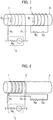
- Fig. 1 is a diagram illustrating an example of a loop antenna according to a first embodiment.
- the loop antenna is a resonant loop antenna including a main loop 1 and an amplifying loop 2.
- the main loop 1 is wound on a bar-shaped rod 3 formed of a magnetic body or an insulation body and is an open loop having terminals T and T that couple a signal source 5 or a (not illustrated) receiving circuit to the main loop 1.
- the number of turns is 1 or more, for example, 5.
- Fig. 1 is a diagram in which the signal source 5 is coupled as an example.
- a resistor R1 and a capacitor C1 are coupled to the main loop 1 in series.
- the amplifying loop 2 is wound on a part of the rod 3 that is different from the part on which the main loop 1 is wound.
- the main loop 1 and the amplifying loop 2 are spaced from each other.
- the amplifying loop 2 is a closed loop including no terminals.
- the number of turns is 1 or more, for example, 5.
- the number of turns may be the same as or different from the number of turns of the main loop 1.
- a resistor R2 and a capacitor C2 are coupled to the main loop 2 in series.
- an alternating current I2 flows through the amplifying loop 2.
- the alternating current I2 becomes greater than the alternating current I1. This allows area expansion of the magnetic field generated by the loop antenna.
- the alternating current I2 depends on multiple elements such as a frequency, the resistor R1, the resistor R2, the capacitor C1, the capacitor C2, an internal resistor R0 of the signal source 5, and a shape of the loop. Thus, it is preferable to adjust respective values of the resistor R1, the resistor R2, the capacitor C1 and the capacitor C2 to maximize the alternating current 12.
- Fig. 1 illustrates the example of a case of coupling the signal source 5 to the loop antenna to use the loop antenna as a transmitting antenna
- the receiving circuit may be coupled to the loop antenna instead of the signal source 5, and the loop antenna may be used as a receiving antenna.
- the alternating current I1 can be maximized by setting respective values of the resistor R1, the resistor R2, the capacitor C1 and the capacitor C2 depending on a frequency and a shape of the loop. Thus, for also the other side, this allows the area expansion of the magnetic field.
- the area expansion of the radio system using the magnetic field is achieved.
- any one or more of the resistor R1, the resistor R2, the capacitor C1 and the capacitor C2 may not be used in some cases. It is the same with the later-described embodiment.
- Fig. 2 is a diagram illustrating an example of a loop antenna according to a second embodiment.
- the main loop 1 and the amplifying loop 2 of the first embodiment are spaced from each other; however, in the second embodiment, the main loop 1 and the amplifying loop 2 are wound on the rod 3 while running side by side. Other configurations are the same with that in the first embodiment.
- the main loop 1 and the amplifying loop 2 since there is the rod 3, the main loop 1 and the amplifying loop 2 generate relatively great magnetic connection.
- the main loop 1 and the amplifying loop 2 run side by side. As a result, the main loop 1 and the amplifying loop 2 are close to each other, thereby generating greater magnetic connection. This allows a greater current to be accumulated in the amplifying loop 2, and thus the area of the magnetic field can further expand.
- the number of turns is arbitrary, and any number of turns is effective.
- the respective numbers of turns of the main loop 1 and the amplifying loop 2 may be different from each other; however, in a case where the number of turns is 2 or more, making the number of turns of the main loop 1 and the number of turns of the amplifying loop 2 equal allows the mutual inductance to be greater, and thus the amplification effect of the current can be enhanced. Hence, it is preferable to make the number of turns of the main loop 1 and the number of turns of the amplifying loop 2 equal.
- a loop antenna of the third embodiment includes optimized capacitors coupled to the main loop 1 and the amplifying loop 2. Other configurations are the same as that of first and second embodiments.
- a frequency f of a signal generated from the signal source 5 is 10 MHz
- the resistor R1 coupled to the main loop 1 is 25 ⁇
- the resistor R2 coupled to the amplifying loop 2 is 1 ⁇
- the internal resistor R0 of the signal source 5 is 25 ⁇ .
- the self-inductance of the loop depends on a geometric shape of the loop.
- Fig. 3 is a diagram illustrating a relationship between the current I2 and the capacitors C1 and C2 of the amplifying loop 2.
- C 1 1 ⁇ 2 L 1 + R 0 + R 1 R 2 ⁇ R 0 + R 1 ⁇ L 2 ⁇ 1
- C 2 1 ⁇ 2 L 1 + R 2 R 0 + R 1 ⁇ R 2 ⁇ L 2 ⁇ 1
- the values of the capacitors C1 and C2 are calculated by using the following equation 2 in which the internal resistor R0 of the signal source 5 of the above equation 1 is changed to an internal resistor R4 of the receiving circuit.
- C 1 1 ⁇ 2 L 1 + R 4 + R 1 R 2 ⁇ R 4 + R 1 ⁇ L 2 ⁇ 1
- C 2 1 ⁇ 2 L 1 + R 2 R 4 + R 1 ⁇ R 2 ⁇ L 2 ⁇ 1
- the current amplification effect becomes maximum at 10 MHz. That is, the current I1 is 10 mA while the current I2 is 70 mA or more. The current I2 is seven times or greater than the current I1. This allows the amplitude of the generatable magnetic field to be amplified seven times or greater. In other words, since the current flowing through the loop antenna can be amplified without increasing the current I1 supplied from the signal source 5, the great magnetic field can be generated with small power consumption. As a result, the area expansion of the radio system using the magnetic field is achieved.
Landscapes
- Engineering & Computer Science (AREA)
- Computer Networks & Wireless Communication (AREA)
- Signal Processing (AREA)
- Near-Field Transmission Systems (AREA)
- Details Of Aerials (AREA)
Abstract
Description
- The present invention relates to a loop antenna that contributes to area expansion of a radio system using a magnetic field.
- Recently, in a short field communication authentication technology such as near field communication (NFC), there is a service performed based on intention and behavior of a user while purposely limiting the authentication area. In a case of forming the authentication area with a magnetic field, a loop antenna (coil) is used, and spherical magnetic field distribution is formed on the antenna surface by allowing a current to flow through the antenna. In the radio system using the magnetic field, the distance attenuation property is more precipitous than that in a system using radio waves, and there is an advantage that a boundary of the radio area can be clearly distinguished; however, in order to widely expand the radio area, increase of an amount of the current supplied from a transmitter is required.
-
- Patent document 1: Japanese Patent Application Publication No.
2013-125991 - Patent document 2: Japanese Patent Application Publication No.
2014-135538 - Patent document 3: Japanese Patent Application Publication No.
2014-135539 - The present invention has been made in view of the above problem, and an objective of the present invention is to provide a small power-consuming loop antenna that contributes to area expansion of the radio system using a magnetic field.
- In order to solve the above problem, a loop antenna of the present invention includes: a main loop that is an open loop coupled to a signal source or a receiving circuit; an amplifying loop that is a closed loop having a same shape as the main loop; a first capacitor that is coupled to the main loop; and a second capacitor that is coupled to the amplifying loop, in which the main loop and the amplifying loop are wound on a bar-shaped rod that is formed of a magnetic body or an insulation body.
- According to the loop antenna of the present invention, in a case of using the signal source, a current that is sufficiently greater than a current flowing through the main loop can be accumulated in the amplifying loop; as a result, it is possible to generate a great magnetic field.
- In addition, according to the loop antenna of the present invention, in a case of using the receiving circuit, due to an effect that a great current is accumulated in the amplifying loop when receiving the magnetic field, the main loop can receive a receiving current that is greater than that in a case of using no amplifying loop.
- As a result of the above, the present invention contributes to the area expansion of the radio system using a magnetic field without significantly increasing power consumption.
-
- [
Fig. 1] Fig. 1 is a diagram illustrating an example of a loop antenna according to a first embodiment. - [
Fig. 2] Fig. 2 is a diagram illustrating an example of a loop antenna according to a second embodiment. - [
Fig. 3] Fig. 3 is a diagram illustrating a relationship between a current I2 and capacitors C1 and C2 of anamplifying loop 2. - [
Fig. 4] Fig. 4 is a diagram illustrating frequency dependence (calculated values) of I1 and I2 when C1 = 31.56 [pF], C2 = 222.09 [pF]. - Embodiments of the present invention are described below referring to the drawings.
-
Fig. 1 is a diagram illustrating an example of a loop antenna according to a first embodiment. - The loop antenna is a resonant loop antenna including a
main loop 1 and anamplifying loop 2. - The
main loop 1 is wound on a bar-shaped rod 3 formed of a magnetic body or an insulation body and is an open loop having terminals T and T that couple asignal source 5 or a (not illustrated) receiving circuit to themain loop 1. The number of turns is 1 or more, for example, 5.Fig. 1 is a diagram in which thesignal source 5 is coupled as an example. A resistor R1 and a capacitor C1 are coupled to themain loop 1 in series. - The amplifying
loop 2 is wound on a part of therod 3 that is different from the part on which themain loop 1 is wound. Themain loop 1 and theamplifying loop 2 are spaced from each other. The amplifyingloop 2 is a closed loop including no terminals. The number of turns is 1 or more, for example, 5. The number of turns may be the same as or different from the number of turns of themain loop 1. A resistor R2 and a capacitor C2 are coupled to themain loop 2 in series. - Once the
main loop 1 is supplied with an alternating current I1 from thesignal source 5, due to the mutual inductance between themain loop 1 and theamplifying loop 2, an alternating current I2 flows through theamplifying loop 2. In general, when a resistance value of the resistor R2 is smaller than a resistance value of the resistor R1, the alternating current I2 becomes greater than the alternating current I1. This allows area expansion of the magnetic field generated by the loop antenna. - The alternating current I2 depends on multiple elements such as a frequency, the resistor R1, the resistor R2, the capacitor C1, the capacitor C2, an internal resistor R0 of the
signal source 5, and a shape of the loop. Thus, it is preferable to adjust respective values of the resistor R1, the resistor R2, the capacitor C1 and the capacitor C2 to maximize thealternating current 12. - Note that, although
Fig. 1 illustrates the example of a case of coupling thesignal source 5 to the loop antenna to use the loop antenna as a transmitting antenna, the receiving circuit may be coupled to the loop antenna instead of thesignal source 5, and the loop antenna may be used as a receiving antenna. - In this case, due to the magnetic field received from outside, a great amount of the alternating current I2 is accumulated in the amplifying
loop 2; however, due to the mutual inductance, also the alternating current I1 flowing through themain loop 1 becomes greater than a case there is noamplifying loop 2. The alternating current I1 can be maximized by setting respective values of the resistor R1, the resistor R2, the capacitor C1 and the capacitor C2 depending on a frequency and a shape of the loop. Thus, for also the other side, this allows the area expansion of the magnetic field. - Hence, according to the loop antenna of the first embodiment, the area expansion of the radio system using the magnetic field is achieved.
- Note that, for example, if a desired current and area can be obtained, any one or more of the resistor R1, the resistor R2, the capacitor C1 and the capacitor C2 may not be used in some cases. It is the same with the later-described embodiment.
-
Fig. 2 is a diagram illustrating an example of a loop antenna according to a second embodiment. - The
main loop 1 and theamplifying loop 2 of the first embodiment are spaced from each other; however, in the second embodiment, themain loop 1 and theamplifying loop 2 are wound on therod 3 while running side by side. Other configurations are the same with that in the first embodiment. - In the first embodiment, since there is the
rod 3, themain loop 1 and theamplifying loop 2 generate relatively great magnetic connection. In the second embodiment, themain loop 1 and the amplifyingloop 2 run side by side. As a result, themain loop 1 and the amplifyingloop 2 are close to each other, thereby generating greater magnetic connection. This allows a greater current to be accumulated in the amplifyingloop 2, and thus the area of the magnetic field can further expand. - In the present invention, the number of turns is arbitrary, and any number of turns is effective. The respective numbers of turns of the
main loop 1 and the amplifyingloop 2 may be different from each other; however, in a case where the number of turns is 2 or more, making the number of turns of themain loop 1 and the number of turns of the amplifyingloop 2 equal allows the mutual inductance to be greater, and thus the amplification effect of the current can be enhanced. Hence, it is preferable to make the number of turns of themain loop 1 and the number of turns of the amplifyingloop 2 equal. - A loop antenna of the third embodiment includes optimized capacitors coupled to the
main loop 1 and the amplifyingloop 2. Other configurations are the same as that of first and second embodiments. - For example, a frequency f of a signal generated from the
signal source 5 is 10 MHz, the resistor R1 coupled to themain loop 1 is 25 Ω, the resistor R2 coupled to the amplifyingloop 2 is 1 Ω, and the internal resistor R0 of thesignal source 5 is 25 Ω. - In addition, self-inductances L of the
main loop 1 and the amplifyingloop 2 are equally 1 µH. - The self-inductance of the loop depends on a geometric shape of the loop. Thus, making the geometric shapes of the
main loop 1 and the amplifyingloop 2 the same easily allows to make these self-inductances equal. -
Fig. 3 is a diagram illustrating a relationship between the current I2 and the capacitors C1 and C2 of the amplifyingloop 2. - Under the above condition, when simulating the current I2 with the capacitor C1 and the capacitor C2 as variables, the result illustrated in
Fig. 3 is obtained. It can be seen that the maximum I2 is obtained when the capacitor C1 is almost 30 pF and the capacitor C2 is almost 220 pF. - Meanwhile, when the above parameters are substituted in the
following equation 1, the capacitor C1 = 31.56 [pF], the capacitor C2 = 222.09 [pF] are obtained. Each frequency ω is calculated by using ω = 2πf. 
- Thus, coupling the capacitors C1 and C2 of the values calculated by using that
equation 1 to themain loop 1 and the amplifyingloop 2 allows the current I2 to be maximized, and the maximum amplification effect can be obtained. - When the receiving circuit is coupled to the
main loop 1, the values of the capacitors C1 and C2 are calculated by using thefollowing equation 2 in which the internal resistor R0 of thesignal source 5 of theabove equation 1 is changed to an internal resistor R4 of the receiving circuit.
-
Fig. 4 is a diagram illustrating frequency dependence (calculated values) of the currents I1 and I2 when C1 = 31.56 [pF], C2 = 222.09 [pF]. - As illustrated in
Fig. 4 , the current amplification effect becomes maximum at 10 MHz. That is, the current I1 is 10 mA while the current I2 is 70 mA or more. The current I2 is seven times or greater than the current I1. This allows the amplitude of the generatable magnetic field to be amplified seven times or greater. In other words, since the current flowing through the loop antenna can be amplified without increasing the current I1 supplied from thesignal source 5, the great magnetic field can be generated with small power consumption. As a result, the area expansion of the radio system using the magnetic field is achieved. -
- 1
- main loop
- 2
- amplifying loop
- 3
- rod
- 5
- signal source
- C1, C2
- capacitor
- I1, I2
- current
- R0, R4
- internal resistor
- R1, R2
- resistor
- T
- terminal
Claims (7)
- A loop antenna comprising:a main loop that is an open loop to be coupled to a signal source or a receiving circuit;an amplifying loop that is a closed loop having a same shape as the main loop;a first capacitor that is coupled to the main loop; anda second capacitor that is coupled to the amplifying loop, whereinthe main loop and the amplifying loop are wound on a bar-shaped rod that is formed of a magnetic body or an insulation body.
- The loop antenna according to claim 1, wherein
the number of turns of the main loop and the number of turns of the amplifying loop are equal. - The loop antenna according to claim 1 or 2, wherein
the main loop and the amplifying loop are spaced from each other. - The loop antenna according to claim 1 or 2, wherein
the main loop and the amplifying loop are wound while running side by side to each other. - The loop antenna according to any one of claims 1 to 4, comprising:a first resistor that is coupled to the first capacitor in series; anda second resistor that is coupled to the second capacitor in series.
- The loop antenna according to claim 5, wherein
the main loop is coupled to the signal source, and when self-inductance of the main loop and self-inductance of the amplifying loop are equal,
the first capacitor C1 of the main loop and the second capacitor C2 of the amplifying loop fulfill conditions of a following equation:
 wherein, L is the self-inductance of the main loop and the amplifying loop,ω is an angular frequency of a signal that is applied to the main loop,R0 is an internal resistor of the signal source,R1 is the first resistor, and R2 is the second resistor.
 - The loop antenna according to claim 5, wherein
the main loop is coupled to the receiving circuit, and
when self-inductance of the main loop and self-inductance of the amplifying loop are equal,
the first capacitor C1 of the main loop and the second capacitor C2 of the amplifying loop fulfill conditions of a following equation: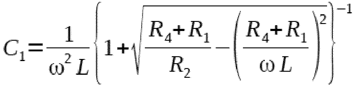
 wherein, L is the self-inductance of the main loop and the amplifying loop,ω is an angular frequency of a signal,R4 is a load resistor of the receiving circuit,R1 is the first resistor, and R2 is the second resistor.
Applications Claiming Priority (2)
| Application Number | Priority Date | Filing Date | Title |
|---|---|---|---|
| JP2016010346A JP6077148B1 (en) | 2016-01-22 | 2016-01-22 | Loop antenna |
| PCT/JP2016/074921 WO2017126151A1 (en) | 2016-01-22 | 2016-08-26 | Loop antenna |
Publications (3)
| Publication Number | Publication Date |
|---|---|
| EP3327864A1 true EP3327864A1 (en) | 2018-05-30 |
| EP3327864A4 EP3327864A4 (en) | 2019-04-17 |
| EP3327864B1 EP3327864B1 (en) | 2019-11-27 |
Family
ID=57981606
Family Applications (1)
| Application Number | Title | Priority Date | Filing Date |
|---|---|---|---|
| EP16886391.8A Active EP3327864B1 (en) | 2016-01-22 | 2016-08-26 | Loop antenna |
Country Status (6)
| Country | Link |
|---|---|
| US (1) | US10454172B2 (en) |
| EP (1) | EP3327864B1 (en) |
| JP (1) | JP6077148B1 (en) |
| KR (1) | KR101950917B1 (en) |
| CN (1) | CN108028465B (en) |
| WO (1) | WO2017126151A1 (en) |
Cited By (1)
| Publication number | Priority date | Publication date | Assignee | Title |
|---|---|---|---|---|
| EP3644439A4 (en) * | 2017-06-20 | 2021-02-24 | Nippon Telegraph and Telephone Corporation | FRAME ANTENNA AND DESIGN PROCESS FOR FRAME ANTENNA |
Family Cites Families (19)
| Publication number | Priority date | Publication date | Assignee | Title |
|---|---|---|---|---|
| JPS58182732A (en) * | 1982-04-20 | 1983-10-25 | Casio Comput Co Ltd | Automatic clearing system |
| US4805232A (en) * | 1987-01-15 | 1989-02-14 | Ma John Y | Ferrite-core antenna |
| WO1996038877A1 (en) * | 1995-05-30 | 1996-12-05 | Sensormatic Electronics Corporation | Eas system antenna configuration for providing improved interrogation field distribution |
| JP2001185939A (en) | 1999-12-24 | 2001-07-06 | Mitsubishi Electric Corp | Antenna coil and electromagnetic induction type non-contact data carrier system |
| DE10107319A1 (en) * | 2000-02-18 | 2002-01-31 | Aisin Seiki | Loop antenna device |
| AU8048701A (en) * | 2000-07-06 | 2002-01-21 | Crane Company C | Twin coil antenna |
| JP3882595B2 (en) * | 2001-11-28 | 2007-02-21 | アイシン精機株式会社 | Antenna device |
| JP2005102101A (en) * | 2003-09-01 | 2005-04-14 | Matsushita Electric Ind Co Ltd | Gate antenna device |
| JP4572555B2 (en) * | 2004-03-25 | 2010-11-04 | パナソニック株式会社 | INSERTION STORAGE MEDIUM DEVICE AND ELECTRONIC DEVICE |
| JP2008259039A (en) * | 2007-04-06 | 2008-10-23 | Alps Electric Co Ltd | Antenna device |
| US8487479B2 (en) * | 2008-02-24 | 2013-07-16 | Qualcomm Incorporated | Ferrite antennas for wireless power transfer |
| WO2009149426A2 (en) * | 2008-06-05 | 2009-12-10 | Qualcomm Incorporated | Ferrite antennas for wireless power transfer |
| JP5218369B2 (en) * | 2009-10-13 | 2013-06-26 | Tdk株式会社 | RFID and wireless communication device |
| JP5684695B2 (en) | 2011-12-13 | 2015-03-18 | 日本電信電話株式会社 | Wireless communication system |
| JP5662954B2 (en) | 2012-02-08 | 2015-02-04 | 株式会社東芝 | Control device and wireless power transmission device |
| KR102144360B1 (en) | 2012-12-05 | 2020-08-13 | 삼성전자주식회사 | Smart nfc antenna matching network system and user device including the same |
| JP5914368B2 (en) | 2013-01-08 | 2016-05-11 | 日本電信電話株式会社 | Portable terminal device and wireless communication system |
| JP5813672B2 (en) | 2013-01-08 | 2015-11-17 | 日本電信電話株式会社 | Wireless communication system |
| CN205657176U (en) * | 2014-02-14 | 2016-10-19 | 株式会社村田制作所 | Antenna device, and wireless communication device |
-
2016
- 2016-01-22 JP JP2016010346A patent/JP6077148B1/en active Active
- 2016-08-26 EP EP16886391.8A patent/EP3327864B1/en active Active
- 2016-08-26 CN CN201680051375.8A patent/CN108028465B/en active Active
- 2016-08-26 US US15/757,249 patent/US10454172B2/en active Active
- 2016-08-26 KR KR1020187006456A patent/KR101950917B1/en active Active
- 2016-08-26 WO PCT/JP2016/074921 patent/WO2017126151A1/en not_active Ceased
Cited By (1)
| Publication number | Priority date | Publication date | Assignee | Title |
|---|---|---|---|---|
| EP3644439A4 (en) * | 2017-06-20 | 2021-02-24 | Nippon Telegraph and Telephone Corporation | FRAME ANTENNA AND DESIGN PROCESS FOR FRAME ANTENNA |
Also Published As
| Publication number | Publication date |
|---|---|
| US20180342806A1 (en) | 2018-11-29 |
| KR101950917B1 (en) | 2019-02-21 |
| KR20180030707A (en) | 2018-03-23 |
| JP2017130863A (en) | 2017-07-27 |
| CN108028465A (en) | 2018-05-11 |
| JP6077148B1 (en) | 2017-02-08 |
| EP3327864A4 (en) | 2019-04-17 |
| US10454172B2 (en) | 2019-10-22 |
| CN108028465B (en) | 2019-03-01 |
| EP3327864B1 (en) | 2019-11-27 |
| WO2017126151A1 (en) | 2017-07-27 |
Similar Documents
| Publication | Publication Date | Title |
|---|---|---|
| US9294154B2 (en) | Enhanced inductive power and data transmission using hyper resonance | |
| US9197986B1 (en) | Electromagnetic induction radio | |
| Jing et al. | Capacity performance of an inductively coupled near field communication system | |
| KR101776991B1 (en) | Wireless power transfer apparatus and method and a method for detecting resonant frequency used in wireless power transfer | |
| US8164530B2 (en) | Antenna formed of multiple resonant loops | |
| CN102918709B (en) | Antenna feed structure and antenna | |
| US10454172B2 (en) | Loop antenna | |
| JP5803550B2 (en) | ANTENNA CIRCUIT, COMMUNICATION DEVICE, AND COMMUNICATION METHOD | |
| EP3273539B1 (en) | Loop antenna | |
| Kim et al. | Comparative study on the power transfer efficiency of magnetic resonance and radio frequency wireless power transmission | |
| JP6240741B2 (en) | Loop antenna | |
| KR101360024B1 (en) | Apparatus and method for transmitting wireless power using capacitors | |
| Oh et al. | Design of Multi-resonant Loop Antenna for Magnetic Induction Communication | |
| CN103545622A (en) | Antenna apparatus and feeding structure thereof | |
| EP3644439B1 (en) | Loop antenna and design method for loop antenna | |
| Heidarian et al. | Optimal coil design for maximum power transfer efficiency in resonantly coupled systems | |
| CN101110655B (en) | Test method and test equipment for radio frequency path | |
| Agbinya et al. | Models and Design of Cooperative Relaying in Inductive Communication Systems | |
| Mohanty et al. | Systematic Analysis to Select Suitable Resonator Topology for Wireless Power Transfer Application | |
| Durnan | Mutual decoupling of collocated loops and coils |
Legal Events
| Date | Code | Title | Description |
|---|---|---|---|
| STAA | Information on the status of an ep patent application or granted ep patent |
Free format text: STATUS: THE INTERNATIONAL PUBLICATION HAS BEEN MADE |
|
| PUAI | Public reference made under article 153(3) epc to a published international application that has entered the european phase |
Free format text: ORIGINAL CODE: 0009012 |
|
| STAA | Information on the status of an ep patent application or granted ep patent |
Free format text: STATUS: REQUEST FOR EXAMINATION WAS MADE |
|
| 17P | Request for examination filed |
Effective date: 20180226 |
|
| AK | Designated contracting states |
Kind code of ref document: A1 Designated state(s): AL AT BE BG CH CY CZ DE DK EE ES FI FR GB GR HR HU IE IS IT LI LT LU LV MC MK MT NL NO PL PT RO RS SE SI SK SM TR |
|
| AX | Request for extension of the european patent |
Extension state: BA ME |
|
| A4 | Supplementary search report drawn up and despatched |
Effective date: 20190314 |
|
| RIC1 | Information provided on ipc code assigned before grant |
Ipc: H04B 5/02 20060101ALI20190308BHEP Ipc: H01Q 7/08 20060101AFI20190308BHEP |
|
| DAV | Request for validation of the european patent (deleted) | ||
| DAX | Request for extension of the european patent (deleted) | ||
| GRAP | Despatch of communication of intention to grant a patent |
Free format text: ORIGINAL CODE: EPIDOSNIGR1 |
|
| STAA | Information on the status of an ep patent application or granted ep patent |
Free format text: STATUS: GRANT OF PATENT IS INTENDED |
|
| INTG | Intention to grant announced |
Effective date: 20190906 |
|
| GRAS | Grant fee paid |
Free format text: ORIGINAL CODE: EPIDOSNIGR3 |
|
| GRAA | (expected) grant |
Free format text: ORIGINAL CODE: 0009210 |
|
| STAA | Information on the status of an ep patent application or granted ep patent |
Free format text: STATUS: THE PATENT HAS BEEN GRANTED |
|
| AK | Designated contracting states |
Kind code of ref document: B1 Designated state(s): AL AT BE BG CH CY CZ DE DK EE ES FI FR GB GR HR HU IE IS IT LI LT LU LV MC MK MT NL NO PL PT RO RS SE SI SK SM TR |
|
| REG | Reference to a national code |
Ref country code: GB Ref legal event code: FG4D |
|
| REG | Reference to a national code |
Ref country code: CH Ref legal event code: EP |
|
| REG | Reference to a national code |
Ref country code: AT Ref legal event code: REF Ref document number: 1207763 Country of ref document: AT Kind code of ref document: T Effective date: 20191215 |
|
| REG | Reference to a national code |
Ref country code: DE Ref legal event code: R096 Ref document number: 602016025322 Country of ref document: DE |
|
| REG | Reference to a national code |
Ref country code: IE Ref legal event code: FG4D |
|
| REG | Reference to a national code |
Ref country code: NL Ref legal event code: MP Effective date: 20191127 |
|
| REG | Reference to a national code |
Ref country code: LT Ref legal event code: MG4D |
|
| PG25 | Lapsed in a contracting state [announced via postgrant information from national office to epo] |
Ref country code: LV Free format text: LAPSE BECAUSE OF FAILURE TO SUBMIT A TRANSLATION OF THE DESCRIPTION OR TO PAY THE FEE WITHIN THE PRESCRIBED TIME-LIMIT Effective date: 20191127 Ref country code: SE Free format text: LAPSE BECAUSE OF FAILURE TO SUBMIT A TRANSLATION OF THE DESCRIPTION OR TO PAY THE FEE WITHIN THE PRESCRIBED TIME-LIMIT Effective date: 20191127 Ref country code: NL Free format text: LAPSE BECAUSE OF FAILURE TO SUBMIT A TRANSLATION OF THE DESCRIPTION OR TO PAY THE FEE WITHIN THE PRESCRIBED TIME-LIMIT Effective date: 20191127 Ref country code: FI Free format text: LAPSE BECAUSE OF FAILURE TO SUBMIT A TRANSLATION OF THE DESCRIPTION OR TO PAY THE FEE WITHIN THE PRESCRIBED TIME-LIMIT Effective date: 20191127 Ref country code: BG Free format text: LAPSE BECAUSE OF FAILURE TO SUBMIT A TRANSLATION OF THE DESCRIPTION OR TO PAY THE FEE WITHIN THE PRESCRIBED TIME-LIMIT Effective date: 20200227 Ref country code: NO Free format text: LAPSE BECAUSE OF FAILURE TO SUBMIT A TRANSLATION OF THE DESCRIPTION OR TO PAY THE FEE WITHIN THE PRESCRIBED TIME-LIMIT Effective date: 20200227 Ref country code: GR Free format text: LAPSE BECAUSE OF FAILURE TO SUBMIT A TRANSLATION OF THE DESCRIPTION OR TO PAY THE FEE WITHIN THE PRESCRIBED TIME-LIMIT Effective date: 20200228 Ref country code: LT Free format text: LAPSE BECAUSE OF FAILURE TO SUBMIT A TRANSLATION OF THE DESCRIPTION OR TO PAY THE FEE WITHIN THE PRESCRIBED TIME-LIMIT Effective date: 20191127 |
|
| PG25 | Lapsed in a contracting state [announced via postgrant information from national office to epo] |
Ref country code: HR Free format text: LAPSE BECAUSE OF FAILURE TO SUBMIT A TRANSLATION OF THE DESCRIPTION OR TO PAY THE FEE WITHIN THE PRESCRIBED TIME-LIMIT Effective date: 20191127 Ref country code: RS Free format text: LAPSE BECAUSE OF FAILURE TO SUBMIT A TRANSLATION OF THE DESCRIPTION OR TO PAY THE FEE WITHIN THE PRESCRIBED TIME-LIMIT Effective date: 20191127 Ref country code: IS Free format text: LAPSE BECAUSE OF FAILURE TO SUBMIT A TRANSLATION OF THE DESCRIPTION OR TO PAY THE FEE WITHIN THE PRESCRIBED TIME-LIMIT Effective date: 20200327 |
|
| PG25 | Lapsed in a contracting state [announced via postgrant information from national office to epo] |
Ref country code: AL Free format text: LAPSE BECAUSE OF FAILURE TO SUBMIT A TRANSLATION OF THE DESCRIPTION OR TO PAY THE FEE WITHIN THE PRESCRIBED TIME-LIMIT Effective date: 20191127 |
|
| PG25 | Lapsed in a contracting state [announced via postgrant information from national office to epo] |
Ref country code: CZ Free format text: LAPSE BECAUSE OF FAILURE TO SUBMIT A TRANSLATION OF THE DESCRIPTION OR TO PAY THE FEE WITHIN THE PRESCRIBED TIME-LIMIT Effective date: 20191127 Ref country code: ES Free format text: LAPSE BECAUSE OF FAILURE TO SUBMIT A TRANSLATION OF THE DESCRIPTION OR TO PAY THE FEE WITHIN THE PRESCRIBED TIME-LIMIT Effective date: 20191127 Ref country code: RO Free format text: LAPSE BECAUSE OF FAILURE TO SUBMIT A TRANSLATION OF THE DESCRIPTION OR TO PAY THE FEE WITHIN THE PRESCRIBED TIME-LIMIT Effective date: 20191127 Ref country code: DK Free format text: LAPSE BECAUSE OF FAILURE TO SUBMIT A TRANSLATION OF THE DESCRIPTION OR TO PAY THE FEE WITHIN THE PRESCRIBED TIME-LIMIT Effective date: 20191127 Ref country code: PT Free format text: LAPSE BECAUSE OF FAILURE TO SUBMIT A TRANSLATION OF THE DESCRIPTION OR TO PAY THE FEE WITHIN THE PRESCRIBED TIME-LIMIT Effective date: 20200419 Ref country code: EE Free format text: LAPSE BECAUSE OF FAILURE TO SUBMIT A TRANSLATION OF THE DESCRIPTION OR TO PAY THE FEE WITHIN THE PRESCRIBED TIME-LIMIT Effective date: 20191127 |
|
| REG | Reference to a national code |
Ref country code: DE Ref legal event code: R097 Ref document number: 602016025322 Country of ref document: DE |
|
| PG25 | Lapsed in a contracting state [announced via postgrant information from national office to epo] |
Ref country code: SK Free format text: LAPSE BECAUSE OF FAILURE TO SUBMIT A TRANSLATION OF THE DESCRIPTION OR TO PAY THE FEE WITHIN THE PRESCRIBED TIME-LIMIT Effective date: 20191127 Ref country code: SM Free format text: LAPSE BECAUSE OF FAILURE TO SUBMIT A TRANSLATION OF THE DESCRIPTION OR TO PAY THE FEE WITHIN THE PRESCRIBED TIME-LIMIT Effective date: 20191127 |
|
| REG | Reference to a national code |
Ref country code: AT Ref legal event code: MK05 Ref document number: 1207763 Country of ref document: AT Kind code of ref document: T Effective date: 20191127 |
|
| PLBE | No opposition filed within time limit |
Free format text: ORIGINAL CODE: 0009261 |
|
| STAA | Information on the status of an ep patent application or granted ep patent |
Free format text: STATUS: NO OPPOSITION FILED WITHIN TIME LIMIT |
|
| 26N | No opposition filed |
Effective date: 20200828 |
|
| PG25 | Lapsed in a contracting state [announced via postgrant information from national office to epo] |
Ref country code: SI Free format text: LAPSE BECAUSE OF FAILURE TO SUBMIT A TRANSLATION OF THE DESCRIPTION OR TO PAY THE FEE WITHIN THE PRESCRIBED TIME-LIMIT Effective date: 20191127 Ref country code: AT Free format text: LAPSE BECAUSE OF FAILURE TO SUBMIT A TRANSLATION OF THE DESCRIPTION OR TO PAY THE FEE WITHIN THE PRESCRIBED TIME-LIMIT Effective date: 20191127 Ref country code: PL Free format text: LAPSE BECAUSE OF FAILURE TO SUBMIT A TRANSLATION OF THE DESCRIPTION OR TO PAY THE FEE WITHIN THE PRESCRIBED TIME-LIMIT Effective date: 20191127 |
|
| PG25 | Lapsed in a contracting state [announced via postgrant information from national office to epo] |
Ref country code: IT Free format text: LAPSE BECAUSE OF FAILURE TO SUBMIT A TRANSLATION OF THE DESCRIPTION OR TO PAY THE FEE WITHIN THE PRESCRIBED TIME-LIMIT Effective date: 20191127 |
|
| PG25 | Lapsed in a contracting state [announced via postgrant information from national office to epo] |
Ref country code: MC Free format text: LAPSE BECAUSE OF FAILURE TO SUBMIT A TRANSLATION OF THE DESCRIPTION OR TO PAY THE FEE WITHIN THE PRESCRIBED TIME-LIMIT Effective date: 20191127 |
|
| REG | Reference to a national code |
Ref country code: CH Ref legal event code: PL |
|
| PG25 | Lapsed in a contracting state [announced via postgrant information from national office to epo] |
Ref country code: CH Free format text: LAPSE BECAUSE OF NON-PAYMENT OF DUE FEES Effective date: 20200831 Ref country code: LU Free format text: LAPSE BECAUSE OF NON-PAYMENT OF DUE FEES Effective date: 20200826 Ref country code: LI Free format text: LAPSE BECAUSE OF NON-PAYMENT OF DUE FEES Effective date: 20200831 |
|
| REG | Reference to a national code |
Ref country code: BE Ref legal event code: MM Effective date: 20200831 |
|
| PG25 | Lapsed in a contracting state [announced via postgrant information from national office to epo] |
Ref country code: BE Free format text: LAPSE BECAUSE OF NON-PAYMENT OF DUE FEES Effective date: 20200831 Ref country code: IE Free format text: LAPSE BECAUSE OF NON-PAYMENT OF DUE FEES Effective date: 20200826 |
|
| PG25 | Lapsed in a contracting state [announced via postgrant information from national office to epo] |
Ref country code: TR Free format text: LAPSE BECAUSE OF FAILURE TO SUBMIT A TRANSLATION OF THE DESCRIPTION OR TO PAY THE FEE WITHIN THE PRESCRIBED TIME-LIMIT Effective date: 20191127 Ref country code: MT Free format text: LAPSE BECAUSE OF FAILURE TO SUBMIT A TRANSLATION OF THE DESCRIPTION OR TO PAY THE FEE WITHIN THE PRESCRIBED TIME-LIMIT Effective date: 20191127 Ref country code: CY Free format text: LAPSE BECAUSE OF FAILURE TO SUBMIT A TRANSLATION OF THE DESCRIPTION OR TO PAY THE FEE WITHIN THE PRESCRIBED TIME-LIMIT Effective date: 20191127 |
|
| PG25 | Lapsed in a contracting state [announced via postgrant information from national office to epo] |
Ref country code: MK Free format text: LAPSE BECAUSE OF FAILURE TO SUBMIT A TRANSLATION OF THE DESCRIPTION OR TO PAY THE FEE WITHIN THE PRESCRIBED TIME-LIMIT Effective date: 20191127 |
|
| PGFP | Annual fee paid to national office [announced via postgrant information from national office to epo] |
Ref country code: DE Payment date: 20250820 Year of fee payment: 10 |
|
| PGFP | Annual fee paid to national office [announced via postgrant information from national office to epo] |
Ref country code: GB Payment date: 20250821 Year of fee payment: 10 |
|
| PGFP | Annual fee paid to national office [announced via postgrant information from national office to epo] |
Ref country code: FR Payment date: 20250828 Year of fee payment: 10 |
|
| REG | Reference to a national code |
Ref country code: DE Ref legal event code: R081 Ref document number: 602016025322 Country of ref document: DE Owner name: NTT, INC., JP Free format text: FORMER OWNER: NIPPON TELEGRAPH AND TELEPHONE CORPORATION, TOKYO, JP Ref country code: DE Ref legal event code: R082 Ref document number: 602016025322 Country of ref document: DE Representative=s name: DENNEMEYER & ASSOCIATES RECHTSANWALTSGESELLSCH, DE |