EP3327795B1 - Thin film and substrate-removed group iii-nitride based devices and method - Google Patents
Thin film and substrate-removed group iii-nitride based devices and method Download PDFInfo
- Publication number
- EP3327795B1 EP3327795B1 EP17202932.4A EP17202932A EP3327795B1 EP 3327795 B1 EP3327795 B1 EP 3327795B1 EP 17202932 A EP17202932 A EP 17202932A EP 3327795 B1 EP3327795 B1 EP 3327795B1
- Authority
- EP
- European Patent Office
- Prior art keywords
- substrate
- epitaxial
- layer
- microns
- thinning
- Prior art date
- Legal status (The legal status is an assumption and is not a legal conclusion. Google has not performed a legal analysis and makes no representation as to the accuracy of the status listed.)
- Active
Links
- 238000000034 method Methods 0.000 title claims description 43
- 239000010409 thin film Substances 0.000 title description 4
- 239000000758 substrate Substances 0.000 claims description 106
- 239000002002 slurry Substances 0.000 claims description 10
- 238000005498 polishing Methods 0.000 claims description 9
- 239000000126 substance Substances 0.000 claims description 6
- 239000002245 particle Substances 0.000 claims description 5
- PIGFYZPCRLYGLF-UHFFFAOYSA-N Aluminum nitride Chemical compound [Al]#N PIGFYZPCRLYGLF-UHFFFAOYSA-N 0.000 claims description 4
- 239000010410 layer Substances 0.000 description 73
- 239000000463 material Substances 0.000 description 34
- 230000008569 process Effects 0.000 description 24
- PMHQVHHXPFUNSP-UHFFFAOYSA-M copper(1+);methylsulfanylmethane;bromide Chemical compound Br[Cu].CSC PMHQVHHXPFUNSP-UHFFFAOYSA-M 0.000 description 20
- 230000006378 damage Effects 0.000 description 10
- 235000012431 wafers Nutrition 0.000 description 10
- 230000007547 defect Effects 0.000 description 8
- 239000000853 adhesive Substances 0.000 description 7
- 230000001070 adhesive effect Effects 0.000 description 7
- 230000008901 benefit Effects 0.000 description 6
- JMASRVWKEDWRBT-UHFFFAOYSA-N Gallium nitride Chemical compound [Ga]#N JMASRVWKEDWRBT-UHFFFAOYSA-N 0.000 description 5
- 238000010521 absorption reaction Methods 0.000 description 5
- 238000013459 approach Methods 0.000 description 5
- 239000010408 film Substances 0.000 description 5
- 239000002131 composite material Substances 0.000 description 4
- 238000013461 design Methods 0.000 description 4
- 229910002601 GaN Inorganic materials 0.000 description 3
- 238000003486 chemical etching Methods 0.000 description 3
- 238000005336 cracking Methods 0.000 description 3
- 229910052751 metal Inorganic materials 0.000 description 3
- 239000002184 metal Substances 0.000 description 3
- 230000005693 optoelectronics Effects 0.000 description 3
- 229910052594 sapphire Inorganic materials 0.000 description 3
- 239000010980 sapphire Substances 0.000 description 3
- IJGRMHOSHXDMSA-UHFFFAOYSA-N Atomic nitrogen Chemical compound N#N IJGRMHOSHXDMSA-UHFFFAOYSA-N 0.000 description 2
- 229910045601 alloy Inorganic materials 0.000 description 2
- 239000000956 alloy Substances 0.000 description 2
- 239000013590 bulk material Substances 0.000 description 2
- 229910003460 diamond Inorganic materials 0.000 description 2
- 239000010432 diamond Substances 0.000 description 2
- 239000002019 doping agent Substances 0.000 description 2
- 238000005530 etching Methods 0.000 description 2
- 238000002474 experimental method Methods 0.000 description 2
- 230000004927 fusion Effects 0.000 description 2
- 238000009499 grossing Methods 0.000 description 2
- 239000012212 insulator Substances 0.000 description 2
- 238000004519 manufacturing process Methods 0.000 description 2
- 239000000203 mixture Substances 0.000 description 2
- 239000004065 semiconductor Substances 0.000 description 2
- 229910052710 silicon Inorganic materials 0.000 description 2
- 239000010703 silicon Substances 0.000 description 2
- 229910002704 AlGaN Inorganic materials 0.000 description 1
- JBRZTFJDHDCESZ-UHFFFAOYSA-N AsGa Chemical compound [As]#[Ga] JBRZTFJDHDCESZ-UHFFFAOYSA-N 0.000 description 1
- ZOXJGFHDIHLPTG-UHFFFAOYSA-N Boron Chemical compound [B] ZOXJGFHDIHLPTG-UHFFFAOYSA-N 0.000 description 1
- GYHNNYVSQQEPJS-UHFFFAOYSA-N Gallium Chemical compound [Ga] GYHNNYVSQQEPJS-UHFFFAOYSA-N 0.000 description 1
- VYPSYNLAJGMNEJ-UHFFFAOYSA-N Silicium dioxide Chemical compound O=[Si]=O VYPSYNLAJGMNEJ-UHFFFAOYSA-N 0.000 description 1
- 238000002679 ablation Methods 0.000 description 1
- 238000004026 adhesive bonding Methods 0.000 description 1
- 239000012790 adhesive layer Substances 0.000 description 1
- 229910052782 aluminium Inorganic materials 0.000 description 1
- XAGFODPZIPBFFR-UHFFFAOYSA-N aluminium Chemical compound [Al] XAGFODPZIPBFFR-UHFFFAOYSA-N 0.000 description 1
- 230000009286 beneficial effect Effects 0.000 description 1
- 238000003339 best practice Methods 0.000 description 1
- 230000015572 biosynthetic process Effects 0.000 description 1
- 229910052796 boron Inorganic materials 0.000 description 1
- -1 carrier Substances 0.000 description 1
- 239000002800 charge carrier Substances 0.000 description 1
- 238000001311 chemical methods and process Methods 0.000 description 1
- 239000008119 colloidal silica Substances 0.000 description 1
- 239000013078 crystal Substances 0.000 description 1
- 238000000151 deposition Methods 0.000 description 1
- 230000008021 deposition Effects 0.000 description 1
- 238000001312 dry etching Methods 0.000 description 1
- 230000000694 effects Effects 0.000 description 1
- 238000010894 electron beam technology Methods 0.000 description 1
- 238000005516 engineering process Methods 0.000 description 1
- 230000005496 eutectics Effects 0.000 description 1
- 230000004907 flux Effects 0.000 description 1
- 238000007499 fusion processing Methods 0.000 description 1
- 229910052733 gallium Inorganic materials 0.000 description 1
- 238000001534 heteroepitaxy Methods 0.000 description 1
- 239000012535 impurity Substances 0.000 description 1
- 229910052738 indium Inorganic materials 0.000 description 1
- APFVFJFRJDLVQX-UHFFFAOYSA-N indium atom Chemical compound [In] APFVFJFRJDLVQX-UHFFFAOYSA-N 0.000 description 1
- 238000002347 injection Methods 0.000 description 1
- 239000007924 injection Substances 0.000 description 1
- 239000011229 interlayer Substances 0.000 description 1
- 230000031700 light absorption Effects 0.000 description 1
- 230000000116 mitigating effect Effects 0.000 description 1
- 238000012986 modification Methods 0.000 description 1
- 230000004048 modification Effects 0.000 description 1
- 229910052757 nitrogen Inorganic materials 0.000 description 1
- 230000003287 optical effect Effects 0.000 description 1
- 230000000737 periodic effect Effects 0.000 description 1
- 230000010287 polarization Effects 0.000 description 1
- 238000007517 polishing process Methods 0.000 description 1
- 238000005086 pumping Methods 0.000 description 1
- 230000006798 recombination Effects 0.000 description 1
- 238000005215 recombination Methods 0.000 description 1
- 230000000717 retained effect Effects 0.000 description 1
- 238000004381 surface treatment Methods 0.000 description 1
- 229910052716 thallium Inorganic materials 0.000 description 1
- BKVIYDNLLOSFOA-UHFFFAOYSA-N thallium Chemical compound [Tl] BKVIYDNLLOSFOA-UHFFFAOYSA-N 0.000 description 1
- 238000000927 vapour-phase epitaxy Methods 0.000 description 1
- 238000001039 wet etching Methods 0.000 description 1
Images

Classifications
-
- H—ELECTRICITY
- H01—ELECTRIC ELEMENTS
- H01L—SEMICONDUCTOR DEVICES NOT COVERED BY CLASS H10
- H01L33/00—Semiconductor devices with at least one potential-jump barrier or surface barrier specially adapted for light emission; Processes or apparatus specially adapted for the manufacture or treatment thereof or of parts thereof; Details thereof
- H01L33/005—Processes
- H01L33/0093—Wafer bonding; Removal of the growth substrate
-
- H—ELECTRICITY
- H01—ELECTRIC ELEMENTS
- H01L—SEMICONDUCTOR DEVICES NOT COVERED BY CLASS H10
- H01L21/00—Processes or apparatus adapted for the manufacture or treatment of semiconductor or solid state devices or of parts thereof
- H01L21/02—Manufacture or treatment of semiconductor devices or of parts thereof
- H01L21/02002—Preparing wafers
- H01L21/02005—Preparing bulk and homogeneous wafers
- H01L21/02008—Multistep processes
- H01L21/0201—Specific process step
-
- H—ELECTRICITY
- H01—ELECTRIC ELEMENTS
- H01L—SEMICONDUCTOR DEVICES NOT COVERED BY CLASS H10
- H01L21/00—Processes or apparatus adapted for the manufacture or treatment of semiconductor or solid state devices or of parts thereof
- H01L21/02—Manufacture or treatment of semiconductor devices or of parts thereof
- H01L21/02104—Forming layers
- H01L21/02365—Forming inorganic semiconducting materials on a substrate
- H01L21/02367—Substrates
- H01L21/0237—Materials
- H01L21/02387—Group 13/15 materials
- H01L21/02389—Nitrides
-
- H—ELECTRICITY
- H01—ELECTRIC ELEMENTS
- H01L—SEMICONDUCTOR DEVICES NOT COVERED BY CLASS H10
- H01L21/00—Processes or apparatus adapted for the manufacture or treatment of semiconductor or solid state devices or of parts thereof
- H01L21/02—Manufacture or treatment of semiconductor devices or of parts thereof
- H01L21/02104—Forming layers
- H01L21/02365—Forming inorganic semiconducting materials on a substrate
- H01L21/02518—Deposited layers
- H01L21/02521—Materials
- H01L21/02538—Group 13/15 materials
- H01L21/0254—Nitrides
-
- H—ELECTRICITY
- H01—ELECTRIC ELEMENTS
- H01L—SEMICONDUCTOR DEVICES NOT COVERED BY CLASS H10
- H01L21/00—Processes or apparatus adapted for the manufacture or treatment of semiconductor or solid state devices or of parts thereof
- H01L21/02—Manufacture or treatment of semiconductor devices or of parts thereof
- H01L21/02104—Forming layers
- H01L21/02365—Forming inorganic semiconducting materials on a substrate
- H01L21/02612—Formation types
- H01L21/02617—Deposition types
- H01L21/02634—Homoepitaxy
-
- H—ELECTRICITY
- H01—ELECTRIC ELEMENTS
- H01L—SEMICONDUCTOR DEVICES NOT COVERED BY CLASS H10
- H01L21/00—Processes or apparatus adapted for the manufacture or treatment of semiconductor or solid state devices or of parts thereof
- H01L21/02—Manufacture or treatment of semiconductor devices or of parts thereof
- H01L21/04—Manufacture or treatment of semiconductor devices or of parts thereof the devices having at least one potential-jump barrier or surface barrier, e.g. PN junction, depletion layer or carrier concentration layer
- H01L21/18—Manufacture or treatment of semiconductor devices or of parts thereof the devices having at least one potential-jump barrier or surface barrier, e.g. PN junction, depletion layer or carrier concentration layer the devices having semiconductor bodies comprising elements of Group IV of the Periodic System or AIIIBV compounds with or without impurities, e.g. doping materials
- H01L21/30—Treatment of semiconductor bodies using processes or apparatus not provided for in groups H01L21/20 - H01L21/26
- H01L21/302—Treatment of semiconductor bodies using processes or apparatus not provided for in groups H01L21/20 - H01L21/26 to change their surface-physical characteristics or shape, e.g. etching, polishing, cutting
- H01L21/306—Chemical or electrical treatment, e.g. electrolytic etching
- H01L21/30625—With simultaneous mechanical treatment, e.g. mechanico-chemical polishing
-
- H—ELECTRICITY
- H01—ELECTRIC ELEMENTS
- H01L—SEMICONDUCTOR DEVICES NOT COVERED BY CLASS H10
- H01L21/00—Processes or apparatus adapted for the manufacture or treatment of semiconductor or solid state devices or of parts thereof
- H01L21/70—Manufacture or treatment of devices consisting of a plurality of solid state components formed in or on a common substrate or of parts thereof; Manufacture of integrated circuit devices or of parts thereof
- H01L21/77—Manufacture or treatment of devices consisting of a plurality of solid state components or integrated circuits formed in, or on, a common substrate
- H01L21/78—Manufacture or treatment of devices consisting of a plurality of solid state components or integrated circuits formed in, or on, a common substrate with subsequent division of the substrate into plural individual devices
- H01L21/7806—Manufacture or treatment of devices consisting of a plurality of solid state components or integrated circuits formed in, or on, a common substrate with subsequent division of the substrate into plural individual devices involving the separation of the active layers from a substrate
-
- H—ELECTRICITY
- H01—ELECTRIC ELEMENTS
- H01L—SEMICONDUCTOR DEVICES NOT COVERED BY CLASS H10
- H01L29/00—Semiconductor devices adapted for rectifying, amplifying, oscillating or switching, or capacitors or resistors with at least one potential-jump barrier or surface barrier, e.g. PN junction depletion layer or carrier concentration layer; Details of semiconductor bodies or of electrodes thereof ; Multistep manufacturing processes therefor
- H01L29/02—Semiconductor bodies ; Multistep manufacturing processes therefor
- H01L29/12—Semiconductor bodies ; Multistep manufacturing processes therefor characterised by the materials of which they are formed
- H01L29/20—Semiconductor bodies ; Multistep manufacturing processes therefor characterised by the materials of which they are formed including, apart from doping materials or other impurities, only AIIIBV compounds
- H01L29/2003—Nitride compounds
-
- H—ELECTRICITY
- H01—ELECTRIC ELEMENTS
- H01L—SEMICONDUCTOR DEVICES NOT COVERED BY CLASS H10
- H01L29/00—Semiconductor devices adapted for rectifying, amplifying, oscillating or switching, or capacitors or resistors with at least one potential-jump barrier or surface barrier, e.g. PN junction depletion layer or carrier concentration layer; Details of semiconductor bodies or of electrodes thereof ; Multistep manufacturing processes therefor
- H01L29/02—Semiconductor bodies ; Multistep manufacturing processes therefor
- H01L29/30—Semiconductor bodies ; Multistep manufacturing processes therefor characterised by physical imperfections; having polished or roughened surface
- H01L29/32—Semiconductor bodies ; Multistep manufacturing processes therefor characterised by physical imperfections; having polished or roughened surface the imperfections being within the semiconductor body
-
- H—ELECTRICITY
- H01—ELECTRIC ELEMENTS
- H01L—SEMICONDUCTOR DEVICES NOT COVERED BY CLASS H10
- H01L33/00—Semiconductor devices with at least one potential-jump barrier or surface barrier specially adapted for light emission; Processes or apparatus specially adapted for the manufacture or treatment thereof or of parts thereof; Details thereof
- H01L33/005—Processes
- H01L33/0062—Processes for devices with an active region comprising only III-V compounds
- H01L33/0075—Processes for devices with an active region comprising only III-V compounds comprising nitride compounds
-
- H—ELECTRICITY
- H01—ELECTRIC ELEMENTS
- H01L—SEMICONDUCTOR DEVICES NOT COVERED BY CLASS H10
- H01L33/00—Semiconductor devices with at least one potential-jump barrier or surface barrier specially adapted for light emission; Processes or apparatus specially adapted for the manufacture or treatment thereof or of parts thereof; Details thereof
- H01L33/02—Semiconductor devices with at least one potential-jump barrier or surface barrier specially adapted for light emission; Processes or apparatus specially adapted for the manufacture or treatment thereof or of parts thereof; Details thereof characterised by the semiconductor bodies
- H01L33/025—Physical imperfections, e.g. particular concentration or distribution of impurities
-
- H—ELECTRICITY
- H01—ELECTRIC ELEMENTS
- H01L—SEMICONDUCTOR DEVICES NOT COVERED BY CLASS H10
- H01L33/00—Semiconductor devices with at least one potential-jump barrier or surface barrier specially adapted for light emission; Processes or apparatus specially adapted for the manufacture or treatment thereof or of parts thereof; Details thereof
- H01L33/02—Semiconductor devices with at least one potential-jump barrier or surface barrier specially adapted for light emission; Processes or apparatus specially adapted for the manufacture or treatment thereof or of parts thereof; Details thereof characterised by the semiconductor bodies
- H01L33/26—Materials of the light emitting region
- H01L33/30—Materials of the light emitting region containing only elements of group III and group V of the periodic system
- H01L33/32—Materials of the light emitting region containing only elements of group III and group V of the periodic system containing nitrogen
-
- H—ELECTRICITY
- H01—ELECTRIC ELEMENTS
- H01S—DEVICES USING THE PROCESS OF LIGHT AMPLIFICATION BY STIMULATED EMISSION OF RADIATION [LASER] TO AMPLIFY OR GENERATE LIGHT; DEVICES USING STIMULATED EMISSION OF ELECTROMAGNETIC RADIATION IN WAVE RANGES OTHER THAN OPTICAL
- H01S5/00—Semiconductor lasers
- H01S5/10—Construction or shape of the optical resonator, e.g. extended or external cavity, coupled cavities, bent-guide, varying width, thickness or composition of the active region
- H01S5/18—Surface-emitting [SE] lasers, e.g. having both horizontal and vertical cavities
- H01S5/183—Surface-emitting [SE] lasers, e.g. having both horizontal and vertical cavities having only vertical cavities, e.g. vertical cavity surface-emitting lasers [VCSEL]
-
- H—ELECTRICITY
- H01—ELECTRIC ELEMENTS
- H01S—DEVICES USING THE PROCESS OF LIGHT AMPLIFICATION BY STIMULATED EMISSION OF RADIATION [LASER] TO AMPLIFY OR GENERATE LIGHT; DEVICES USING STIMULATED EMISSION OF ELECTROMAGNETIC RADIATION IN WAVE RANGES OTHER THAN OPTICAL
- H01S5/00—Semiconductor lasers
- H01S5/30—Structure or shape of the active region; Materials used for the active region
- H01S5/32—Structure or shape of the active region; Materials used for the active region comprising PN junctions, e.g. hetero- or double- heterostructures
- H01S5/323—Structure or shape of the active region; Materials used for the active region comprising PN junctions, e.g. hetero- or double- heterostructures in AIIIBV compounds, e.g. AlGaAs-laser, InP-based laser
- H01S5/32308—Structure or shape of the active region; Materials used for the active region comprising PN junctions, e.g. hetero- or double- heterostructures in AIIIBV compounds, e.g. AlGaAs-laser, InP-based laser emitting light at a wavelength less than 900 nm
-
- H—ELECTRICITY
- H01—ELECTRIC ELEMENTS
- H01S—DEVICES USING THE PROCESS OF LIGHT AMPLIFICATION BY STIMULATED EMISSION OF RADIATION [LASER] TO AMPLIFY OR GENERATE LIGHT; DEVICES USING STIMULATED EMISSION OF ELECTROMAGNETIC RADIATION IN WAVE RANGES OTHER THAN OPTICAL
- H01S2304/00—Special growth methods for semiconductor lasers
- H01S2304/04—MOCVD or MOVPE
Definitions
- This disclosure relates to a method of thinning a substrate or removing the substrate, more particularly to aluminum nitride substrates.
- Aluminum nitride (AlN) and AlN epitaxial films grown on bulk AlN substrates have several uses due to the unique properties of the AlN material system-particularly its very high band gap energy.
- the substrate may need to undergo extreme thinning, such as to less than 20 microns, or be completely removed.
- extreme thinning such as to less than 20 microns, or be completely removed.
- One such example consists of a UV-C VECSEL (vertical external cavity surface emitter lasers) device emitting near 240nm.
- VECSEL vertical external cavity surface emitter lasers
- the term 'bulk AlN' refers to AlN single crystalline AlN boules that are sectioned into wafers on which epitaxial material is grown.
- substrate removal is typically employed for devices grown heteroepitaxially on non-native substrates.
- the substrate removal processes typically exploit material differences that exist between the substrate and epitaxial layers to remove the substrate while maintaining the device layers intact.
- a laser lift-off process can remove gallium nitride (GaN) blue LED device layers grown on sapphire.
- the laser employs a wavelength transparent in sapphire but absorbed by GaN.
- Selective ablation at the substrate/epitaxial layer interface causes the epitaxial layer to separate from the substrate.
- Other examples include AlGaInP LED device layers grown on red light absorbing gallium arsenide (GaAs) substrates.
- the substrate is removed by a chemically selective wet etch that attacks the substrate but not the device layers.
- Another example involves separating device layers by photo-electrochemical (PEC) undercut etching of a strategically located n-type epitaxial material layer.
- PEC photo-electrochemical
- One embodiment is a method of thinning a bulk aluminum nitride substrate, including providing a bulk aluminum nitride (AlN) substrate with at least one epitaxially grown group-III-nitride layer on a first side of the substrate, applying a slurry having a high pH to a second side of the substrate opposite the first side, chemical mechanically polishing the second side of the substrate using the slurry to remove at least a portion of the substrate, resulting in a thinned layer with a thickness less than 50 microns, and bonding the epitaxial layer to a non-native substrate.
- AlN bulk aluminum nitride
- Another embodiment which is not part of the invention, is a device including at least one active zone in a layer of epitaxial Group-III-nitride material, the epitaxial Group-III-nitride layer having a defect density of less than or equal to 10 8 /cm 2 .
- epitaxial processes can now epitaxially grow material and produce devices on 'native' substrates such as gallium nitride (GaN) and aluminum nitride (AlN).
- GaN gallium nitride
- AlN aluminum nitride
- the term 'native' as used here means that the epitaxial layer consists of the same material as the substrate. The discussion may refer to the substrate as the 'bulk' substrate to differentiate it from the epitaxial layer.
- thinning and substrate removal will be referred to collectively as thinning the substrate.
- removing the substrate is an extension of the thinning process to the point where no substrate remains.
- Many of the currently available substrate removal processes do not work for epitaxially grown GaN or AlN.
- PEC photo-electro chemical etching
- p-type doping is currently very problematic for AlN substrates and epitaxial layers, making PEC unlikely to be an effective tool.
- Another approach would use an epitaxially grown layer to form an etch stop or differentially light absorbing layer.
- Many devices formed in the epitaxial layer rely on the high quality gained by epitaxially growth, so etch stops or light absorbing layers with sufficiently contrasting properties are counter to this quality.
- conventional mechanical thinning while an obvious consideration, has a low probability for success.
- Conventional mechanical thinning works on softer materials, such as silicon. AlN and wide band gap materials more generally, lie at the other extreme, having a high hardness.
- Conventional mechanical thinning process would have to be highly aggressive to produce acceptable material removal rates. This would require large abrasive particle size and high force, which causes cracking and sub-surface damage that would extend deep into the substrate and eventually into the device layers themselves.
- the patent also does not apply chemical mechanical polishing for material removal, just for smoothing a surface for epitaxial growth.
- a similar patent, 7,323,414 also addresses mechanical polishing for smoothing a surface, but not full removal of the material.
- CMP chemical mechanical polishing
- etching also has issues as a thinning, substrate removal process, or even damage removal method. Inserting a sufficiently thick etch stop layer with acceptable etch robustness into the epitaxial structure would relinquish the benefits that result from a epitaxially grown layer on a native substrate. Epitaxial growth has the advantage of no lattice mismatch between the substrate and the epitaxial layers, an advantage which is lost for sufficiently thick layers with substitute atoms of differing lattice parameter.
- Group III-Nitride material systems have known crystallographic asymmetry and polarization fields that result in a strong tendency toward anisotropic behavior during chemical etching.
- group-III materials are those identified by Group 3 on the Periodic Table of the elements and include aluminum (Al), Indium (In), Gallium (Ga), Thallium (Tl), and Boron (B).
- Al aluminum
- Indium In
- Ga Gallium
- Tl Thallium
- B Boron
- the group III oriented face is seen to be extremely chemically inert. This anisotropy is observed for both wet and dry etching processes. Whether the etch is wet or dry, chemical, or electrochemical, surface smoothness or planarity will not be preserved for material removal processes that lack any mechanically abrasive planarizing component., This is expected to hold true for both bulk material removal etches and clean up etches used to remove physically created damage. The implication is that a chemical process for removing damage is likely to compromise the surface flatness required for many device applications. In summary, existing methods cannot remove or thin substrates below 20 microns or give rise to other issues.
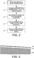
- Figure 1 shows an embodiment of a device 10 mounted on a carrier 16.
- the carrier 16 has perforations such as 18 in this example.
- the layer 12 may be mounted on the carrier 16 using a layer of adhesive 14.
- the layer stack 12 may contain optoelectronic device heterostructures or a device that relies upon a very thin substrate, or upon the substrate being completely removed. As discussed above, these device heterostructures may consist of vertical external cavity surface emitter lasers (VECSELs), distributed Bragg reflectors (DBRs), thin film ergodic LEDs, silicon on insulator (SOI), radio frequency devices, etc.
- VECSELs vertical external cavity surface emitter lasers
- DBRs distributed Bragg reflectors
- SOI silicon on insulator
- Examples of devices that require substrate thinning or removal include UV-C (UV light having a wavelength in the 100 - 280 nanometer range) VECSELs, mentioned before, and UV-C LEDs.
- a VECSEL is a laser device in which the charge carriers are injected by means of an electron beam originating relatively far from the laser cavity, both of which are contained in a vacuum.
- the laser cavity consists of layers of AlN and AlGaN alloys with specific composition and structure so as to generate the necessary conditions for lasing.
- the bulk material despite having low defect density, still has impurity dopant/defect concentrations that cause the material to be absorbing at UV-C wavelengths. Even a single micron of bulk substrate material remaining would result in catastrophic absorption levels, given the multiple passes through the material making up the cavity.
- MOVPE metal organic vapor phase epitaxy
- the process does not incorporate these levels of dopants/defects resulting in a material comparably transparent even at UV-C wavelengths.
- the epitaxial layers need to be fused to a thermal heat sink substrate such as diamond.
- the highly planar, smooth, and damage free surface produced by the methods here enable this wafer fusion process.
- Another example consists of a UV-C LED, whether powered externally by e-beam pumping in vacuum or by conventional electrical injection in a p-/n-junction diode.
- One common LED chip design is the so-called 'thin-chip' or 'thin-film flip-chip' design. Cell phone camera flashes typically employ this design, for example.
- the design works by having a cavity, where instead of mode minimized coherence, its opposite, ergodicity, is obtain. In this approach, light not 'extracted' from the high index crystal layers reflects in a randomized, mostly loss free, manner until it arrives at a trajectory that allows it to escape to the outside world. Therefore, the cavity should be highly transparent.
- approaches to LEDs exist that involve fusing the epitaxial layers to a second substrate material that has desirable light extracting, thermal, and or mechanical properties. This approach also would benefit from fusion to a smooth substrate free epitaxial layer.
- the process starts at 20 in Figure 2 by growing an epitaxial layer 32 on a bulk AlN substrate 30 in Figure 3 .
- the epitaxial layer may contain optoelectronic or other types of electronic devices in at least a portion or zone 34 of the epitaxial layer.
- the region 32 identifies a portion of the epitaxial layer that protects the layer 34 from being removed or thinned.
- the combination of the bulk AlN substrate and the epitaxial layer will be referred to here as the composite substrate.
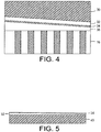
- the process next adheres the composite substrate to a carrier wafer in 22 of Figure 2 .
- a perforated sapphire substrate 16 receives a spin coated adhesive 36 in Figure 4 .
- the composite substrate of the substrate 30, and epitaxial layers 32 and 34 is then mounted on the carrier to provide mechanical support during chemical mechanical planarization. Note that the composite substrate is rotated to be 'upside down.'
- a soft polishing pad applies a relatively high pH slurry having abrasive particles to the bulk AlN substrate.
- a 'high pH' slurry consists of a slurry having a pH in the base range of about 9.5 or higher.
- the slurry consists of a colloidal silica having a pH of 9.8.
- the particle size may vary, but in some embodiments they have a size ranging from 0.02 microns to 0.05 microns. Smaller particle sizes result in slower material removal rates (MRR), but may reduce the chance of any defects being caused by the process and result in greater surface smoothness.
- the resulting device heterostructures may only consist of the device layer 34 and portions of 32.
- the epitaxial layer can be transferred from the carrier substrate and, for example, bonded to a heat sink such as diamond, mentioned above and shown at 26 in Figure 2 .
- the carrier wafer is then removed at 28, leaving only the portion 34 and 32 of the epitaxial layer adhered to the heat sink substrate 40 by means of a direct bond.
- the direct bonding process may involve surface treatments, interlayer depositions, pressure, and/or heat to cause the material of the epitaxial layer to bond to the heat sink without using any adhesives.
- adhesive bonding, metal-metal bonding, metal eutectic bonding, and anodic bonding may also have advantages depending upon the application.
- the epitaxial layer may also be bonded to a different non-native substrate, other than the heat sink, where a non-native substrate is any substrate that is not the substrate upon which it was created.
- Planarity is commonly expressed as total thickness variation (TTV) and represents the numerical thickness difference between the thickest and thinnest portions of the wafer or sample stack.
- the epitaxial layers such as 32 and 34 are typically of the order of a few microns, whereas the substrate 30 is typically hundreds of microns.
- the carrier wafer 16 as well is typically several hundreds of microns or even over 1mm thick.
- An adhesive layer such as 36 is typically in the microns or tens of microns range. The summation of all these layers yields the TTV of the entire stack.
- the epitaxial device layers are hundreds of times thinner than the substrate, carrier, and adhesive stack. If the TTV of the entire stack is greater than the thickness of the epitaxial device layers, the device layers will be removed entirely at the thickest portion of the stack, whereas substrate material will remain at the thinnest portion of the stack. In addition, the material removal process introduces additional deviation from planarity, such as due to axial aparallelism of polishing equipment components. Given these considerations, great attention is required to maintaining low TTV in the epi/substrate/adhesive/carrier stack. Despite best efforts, some non-zero TTV is unavoidable.
- the epitaxial layer allows for an expanded TTV allowance.
- the epitaxial layer is greater than a particular thickness, all the substrate can safely be removed while not risking total removal of the epitaxial layer where the total thickness of the stack is high.
- the particular thickness may depend upon the total thickness variation obtainable by the thinning and polishing processes used. For example, in some experiments if the epitaxial layer is greater than 12 microns thick, the entire substrate may be removed with the entire device layer remaining. If the epitaxial layer is less than 12 microns thick, to prevent potentially catastrophic 'punch through' during thinning, some of the substrate may be unavoidably retained for typical TTV values and CMP methods employed.
- Growing thick epitaxial layers with beneficial properties such as low light absorption represents another important aspect of the invention.
- the resulting device in the case where the entire substrate has been removed, may appear to be very similar in structure to devices grown using heteroepitaxy, since the relationship between the layers and the substrate is no longer relevant, and the process of how the layer came into existence is not detectable from the layer itself.
- the level of defects define here as threading dislocations, in pseudomorphically grown epitaxial films lies far below the level of defects grown on a non-native substrate.
- the reference to pseudomorphically grown epitaxial films used here is a characteristic of the layer, not a reference to the process by which it is made.
- the pseudomorphically grown epitaxial films typically have a threading dislocation density below 10 8 /cm 2 , and can be as low as 10 3 /cm 2 to 10 5 /cm 2 .
- Psuedomorphic growth refers to the process whereby a thin layer of material differing in composition from the underlying substrate, often alloys of the substrate, are grown in a strained state such that the otherwise different lattice parameter matches that of the substrate. Threading dislocations are a class of defects, typically resulting from lattice mismatch between the substrate and epitaxial films, known to lead to light output efficiency reducing non-radiative carrier recombination.
Description
- This disclosure relates to a method of thinning a substrate or removing the substrate, more particularly to aluminum nitride substrates.
- Aluminum nitride (AlN) and AlN epitaxial films grown on bulk AlN substrates have several uses due to the unique properties of the AlN material system-particularly its very high band gap energy. In some instances, the substrate may need to undergo extreme thinning, such as to less than 20 microns, or be completely removed. One such example consists of a UV-C VECSEL (vertical external cavity surface emitter lasers) device emitting near 240nm. The term 'bulk AlN' refers to AlN single crystalline AlN boules that are sectioned into wafers on which epitaxial material is grown.
- Vertical lasers rely on light traversing the laser cavity multiple times. This requires that the reflectors be highly efficient, and that the cavity have very low absorption. At UV-C wavelengths, bulk AlN substrates exhibit absorption loss to the degree that even a micron of substrate material in the cavity would inhibit the gain necessary for successful lasing. Removing the substrate, leaving only higher quality epitaxial material in the cavity, becomes an essential process and device structure. Thin film ergodic LED devices represent another example where light must traverse a low loss cavity multiple times. Substrate removal can also provide benefits to electronic devices. In addition, substrate-removed devices may be fused or bonded onto substrates with superior properties to the one upon which they were formed. Substrate thinning or complete removal and subsequent bonding or fusion can enable devices that require a thin channel in contact with a contrasting material, such as semiconductor on insulator (SOI) and radio frequency devices.
- For class III-V semiconductor devices substrate removal is typically employed for devices grown heteroepitaxially on non-native substrates. In this case, the substrate removal processes typically exploit material differences that exist between the substrate and epitaxial layers to remove the substrate while maintaining the device layers intact.
- For example, a laser lift-off process can remove gallium nitride (GaN) blue LED device layers grown on sapphire. The laser employs a wavelength transparent in sapphire but absorbed by GaN. Selective ablation at the substrate/epitaxial layer interface causes the epitaxial layer to separate from the substrate. Other examples include AlGaInP LED device layers grown on red light absorbing gallium arsenide (GaAs) substrates. The substrate is removed by a chemically selective wet etch that attacks the substrate but not the device layers. Another example involves separating device layers by photo-electrochemical (PEC) undercut etching of a strategically located n-type epitaxial material layer.
- One embodiment is a method of thinning a bulk aluminum nitride substrate, including providing a bulk aluminum nitride (AlN) substrate with at least one epitaxially grown group-III-nitride layer on a first side of the substrate, applying a slurry having a high pH to a second side of the substrate opposite the first side, chemical mechanically polishing the second side of the substrate using the slurry to remove at least a portion of the substrate, resulting in a thinned layer with a thickness less than 50 microns, and bonding the epitaxial layer to a non-native substrate.
- Another embodiment, which is not part of the invention, is a device including at least one active zone in a layer of epitaxial Group-III-nitride material, the epitaxial Group-III-nitride layer having a defect density of less than or equal to 108/cm2.
-
-
Figure 1 shows a epitaxial AlN-based wafer on a carrier. -
Figure 2 shows a flowchart of one embodiment of a method of thinning an AlN substrate. -
Figures 3-5 show various stages of a device undergoing manufacture. - With recent advances in substrate growth technology, epitaxial processes can now epitaxially grow material and produce devices on 'native' substrates such as gallium nitride (GaN) and aluminum nitride (AlN). The term 'native' as used here means that the epitaxial layer consists of the same material as the substrate. The discussion may refer to the substrate as the 'bulk' substrate to differentiate it from the epitaxial layer.
- The ability to epitaxially grow these materials enables highly defect-free material and new devices, many of which require substrate removal or thinning. The lack of material behavior 'contrast' between the substrate and the epitaxial layers precludes many of the methods typically employed for substrate thinning and removal. For purposes of simplifying the discussion, thinning and substrate removal will be referred to collectively as thinning the substrate.
- Essentially, in the embodiments here, removing the substrate is an extension of the thinning process to the point where no substrate remains. Many of the currently available substrate removal processes do not work for epitaxially grown GaN or AlN. Specifically, photo-electro chemical etching (PEC) based approaches have been found to be ineffective for AlN substrate removal. p-type doping is currently very problematic for AlN substrates and epitaxial layers, making PEC unlikely to be an effective tool. Another approach, would use an epitaxially grown layer to form an etch stop or differentially light absorbing layer. Many devices formed in the epitaxial layer rely on the high quality gained by epitaxially growth, so etch stops or light absorbing layers with sufficiently contrasting properties are counter to this quality.
- Similarly, conventional mechanical thinning, while an obvious consideration, has a low probability for success. Conventional mechanical thinning works on softer materials, such as silicon. AlN and wide band gap materials more generally, lie at the other extreme, having a high hardness. Conventional mechanical thinning process would have to be highly aggressive to produce acceptable material removal rates. This would require large abrasive particle size and high force, which causes cracking and sub-surface damage that would extend deep into the substrate and eventually into the device layers themselves.
- Experiments have shown that upon thinning substrates to a thickness of approximately 30 microns, the mechanical thinning process destroys the mechanical integrity of the sample, meaning cracking extends through the entirety of the sample, at which point it no longer adheres to the mounting chuck. This will likely limit substrate thicknesses to a value greater than 30 microns, noting that sub-surface damage will extend throughout the device layers before cracking has led to the obvious destruction of the sample. Thicknesses near 30 microns with useable device layers may be possible, but would likely require prohibitively time consuming abrasive steps with extremely low material removal rates, such as orders of magnitude lower than typical rates. Furthermore, sub-surface damage created by conventional thinning notoriously creates light absorbing regions, regardless of the final thickness reached. This absorption can severely impair device functionality for optoelectronic devices.
- For these reasons, conventional abrasive based thinning is not expected to enable devices below 30 microns in thickness and cannot achieve complete substrate removal for reasonable epitaxial layer thicknesses. For devices where near perfect optical transparency is critical, mechanical thinning cannot be used at all without some sort of mitigating processes, such as damage removal etch. Evidence of the above can be found in a patent application
US Patent 9,299,883 7,323,414 WO 03/043780 A2 WO 2008/088838 A1 . - Purely chemical etching also has issues as a thinning, substrate removal process, or even damage removal method. Inserting a sufficiently thick etch stop layer with acceptable etch robustness into the epitaxial structure would relinquish the benefits that result from a epitaxially grown layer on a native substrate. Epitaxial growth has the advantage of no lattice mismatch between the substrate and the epitaxial layers, an advantage which is lost for sufficiently thick layers with substitute atoms of differing lattice parameter.
- Group III-Nitride material systems have known crystallographic asymmetry and polarization fields that result in a strong tendency toward anisotropic behavior during chemical etching. As used here, group-III materials are those identified by Group 3 on the Periodic Table of the elements and include aluminum (Al), Indium (In), Gallium (Ga), Thallium (Tl), and Boron (B). When etching is carried out on the nitrogen face, which is generally the case for the conventional orientation of group III-nitride substrates, the material is seen to be highly reactive, either chemically as in the case of AlN and/or electrochemically in the case of GaN.
- In sharp contrast, the group III oriented face is seen to be extremely chemically inert. This anisotropy is observed for both wet and dry etching processes. Whether the etch is wet or dry, chemical, or electrochemical, surface smoothness or planarity will not be preserved for material removal processes that lack any mechanically abrasive planarizing component., This is expected to hold true for both bulk material removal etches and clean up etches used to remove physically created damage. The implication is that a chemical process for removing damage is likely to compromise the surface flatness required for many device applications. In summary, existing methods cannot remove or thin substrates below 20 microns or give rise to other issues.
-
Figure 1 shows an embodiment of adevice 10 mounted on acarrier 16. Thecarrier 16 has perforations such as 18 in this example. Thelayer 12 may be mounted on thecarrier 16 using a layer ofadhesive 14. Thelayer stack 12 may contain optoelectronic device heterostructures or a device that relies upon a very thin substrate, or upon the substrate being completely removed. As discussed above, these device heterostructures may consist of vertical external cavity surface emitter lasers (VECSELs), distributed Bragg reflectors (DBRs), thin film ergodic LEDs, silicon on insulator (SOI), radio frequency devices, etc. - Examples of devices that require substrate thinning or removal include UV-C (UV light having a wavelength in the 100 - 280 nanometer range) VECSELs, mentioned before, and UV-C LEDs. Very simply, a VECSEL is a laser device in which the charge carriers are injected by means of an electron beam originating relatively far from the laser cavity, both of which are contained in a vacuum. The laser cavity consists of layers of AlN and AlGaN alloys with specific composition and structure so as to generate the necessary conditions for lasing. As lasing requires stimulated emission, a high photon flux through the active region is necessary. In effect this means that generated photons traverse the cavity many times, necessitating high reflectance from either side of the cavity, and extremely low absorption within the cavity. This last constraint requires the removal of the substrate.
- The bulk material, despite having low defect density, still has impurity dopant/defect concentrations that cause the material to be absorbing at UV-C wavelengths. Even a single micron of bulk substrate material remaining would result in catastrophic absorption levels, given the multiple passes through the material making up the cavity. Because the growth method for the epitaxial layers here is MOVPE (metal organic vapor phase epitaxy), the process does not incorporate these levels of dopants/defects resulting in a material comparably transparent even at UV-C wavelengths. There are other relevant aspects to this device. For instance, the epitaxial layers need to be fused to a thermal heat sink substrate such as diamond. The highly planar, smooth, and damage free surface produced by the methods here enable this wafer fusion process.
- Another example consists of a UV-C LED, whether powered externally by e-beam pumping in vacuum or by conventional electrical injection in a p-/n-junction diode. One common LED chip design is the so-called 'thin-chip' or 'thin-film flip-chip' design. Cell phone camera flashes typically employ this design, for example. The design works by having a cavity, where instead of mode minimized coherence, its opposite, ergodicity, is obtain. In this approach, light not 'extracted' from the high index crystal layers reflects in a randomized, mostly loss free, manner until it arrives at a trajectory that allows it to escape to the outside world. Therefore, the cavity should be highly transparent. In addition, approaches to LEDs exist that involve fusing the epitaxial layers to a second substrate material that has desirable light extracting, thermal, and or mechanical properties. This approach also would benefit from fusion to a smooth substrate free epitaxial layer.
- Turning now to
Figure 2 , the discussion turns to the formation of the device.Figure 2 will be discussed with regard toFigures 3-5 showing the stages of manufacture. In one embodiment, the process starts at 20 inFigure 2 by growing anepitaxial layer 32 on abulk AlN substrate 30 inFigure 3 . The epitaxial layer may contain optoelectronic or other types of electronic devices in at least a portion orzone 34 of the epitaxial layer. Theregion 32 identifies a portion of the epitaxial layer that protects thelayer 34 from being removed or thinned. The combination of the bulk AlN substrate and the epitaxial layer will be referred to here as the composite substrate. - The process next adheres the composite substrate to a carrier wafer in 22 of
Figure 2 . In this embodiment, aperforated sapphire substrate 16 receives a spin coated adhesive 36 inFigure 4 . The composite substrate of thesubstrate 30, andepitaxial layers - The CMP process applied at 24 in
Figure 2 may take many forms. In one embodiment, a soft polishing pad applies a relatively high pH slurry having abrasive particles to the bulk AlN substrate. As used here, a 'high pH' slurry consists of a slurry having a pH in the base range of about 9.5 or higher. In one embodiment, the slurry consists of a colloidal silica having a pH of 9.8. The particle size may vary, but in some embodiments they have a size ranging from 0.02 microns to 0.05 microns. Smaller particle sizes result in slower material removal rates (MRR), but may reduce the chance of any defects being caused by the process and result in greater surface smoothness. - The resulting device heterostructures may only consist of the
device layer 34 and portions of 32. After this point, the epitaxial layer can be transferred from the carrier substrate and, for example, bonded to a heat sink such as diamond, mentioned above and shown at 26 inFigure 2 . The carrier wafer is then removed at 28, leaving only theportion heat sink substrate 40 by means of a direct bond. The direct bonding process may involve surface treatments, interlayer depositions, pressure, and/or heat to cause the material of the epitaxial layer to bond to the heat sink without using any adhesives. However, adhesive bonding, metal-metal bonding, metal eutectic bonding, and anodic bonding may also have advantages depending upon the application. The epitaxial layer may also be bonded to a different non-native substrate, other than the heat sink, where a non-native substrate is any substrate that is not the substrate upon which it was created. - In addition to the damage free and high material removal rate discussed above, the substrate removal or extreme substrate thinning process requires very stringent planarity control of the entire substrate, adhesive, and carrier wafer stack. Planarity is commonly expressed as total thickness variation (TTV) and represents the numerical thickness difference between the thickest and thinnest portions of the wafer or sample stack.
- It should be noted that the epitaxial layers such as 32 and 34 are typically of the order of a few microns, whereas the
substrate 30 is typically hundreds of microns. Thecarrier wafer 16 as well is typically several hundreds of microns or even over 1mm thick. An adhesive layer such as 36 is typically in the microns or tens of microns range. The summation of all these layers yields the TTV of the entire stack. - It should be noted that the epitaxial device layers are hundreds of times thinner than the substrate, carrier, and adhesive stack. If the TTV of the entire stack is greater than the thickness of the epitaxial device layers, the device layers will be removed entirely at the thickest portion of the stack, whereas substrate material will remain at the thinnest portion of the stack. In addition, the material removal process introduces additional deviation from planarity, such as due to axial aparallelism of polishing equipment components. Given these considerations, great attention is required to maintaining low TTV in the epi/substrate/adhesive/carrier stack. Despite best efforts, some non-zero TTV is unavoidable.
- For example, in
Figures 3 and4 , one can see the variation of the top of the substrate reflected in theepitaxial layer 32 andportion 34. At the bonding step, where the substrate wafer and epitaxial layer is attached to the carrier wafer, a high degree of planarity is achieved through best practices. This planarity constraint between the carrier backside and the substrate backside carries through the adhesive 36, which alleviates some of the thickness variation by 'absorbing' the difference. In the finalmounted layers - Growing a thicker epitaxial layer allows for an expanded TTV allowance. Generally, if the epitaxial layer is greater than a particular thickness, all the substrate can safely be removed while not risking total removal of the epitaxial layer where the total thickness of the stack is high. The particular thickness may depend upon the total thickness variation obtainable by the thinning and polishing processes used. For example, in some experiments if the epitaxial layer is greater than 12 microns thick, the entire substrate may be removed with the entire device layer remaining. If the epitaxial layer is less than 12 microns thick, to prevent potentially catastrophic 'punch through' during thinning, some of the substrate may be unavoidably retained for typical TTV values and CMP methods employed. Growing thick epitaxial layers with beneficial properties such as low light absorption represents another important aspect of the invention.
- The resulting device, in the case where the entire substrate has been removed, may appear to be very similar in structure to devices grown using heteroepitaxy, since the relationship between the layers and the substrate is no longer relevant, and the process of how the layer came into existence is not detectable from the layer itself. However, the level of defects, define here as threading dislocations, in pseudomorphically grown epitaxial films lies far below the level of defects grown on a non-native substrate. One should note that the reference to pseudomorphically grown epitaxial films used here is a characteristic of the layer, not a reference to the process by which it is made. In many of the embodiments here, the pseudomorphically grown epitaxial films typically have a threading dislocation density below 108/cm2, and can be as low as 103/cm2 to 105/cm2.
- Psuedomorphic growth refers to the process whereby a thin layer of material differing in composition from the underlying substrate, often alloys of the substrate, are grown in a strained state such that the otherwise different lattice parameter matches that of the substrate. Threading dislocations are a class of defects, typically resulting from lattice mismatch between the substrate and epitaxial films, known to lead to light output efficiency reducing non-radiative carrier recombination.
- It will be appreciated that variants of the above-disclosed and other features and functions, or alternatives thereof, may be combined into many other different systems or applications. Various presently unforeseen or unanticipated alternatives, modifications, variations, or improvements therein may be subsequently made by those skilled in the art which are also intended to be encompassed by the following claims.
Claims (7)
- A method of thinning a bulk aluminum nitride (AlN) substrate (30) with at least one epitaxially grown group-III-nitride layer (32, 34) provided on a first side of the substrate, the method comprising:applying (24) a slurry having a high pH to a second side of the substrate (30) opposite the first side;chemical mechanically polishing the second side of the substrate (30) using the slurry to remove at least a portion of the substrate, resulting in a thinned layer (32, 34) with a thickness less than 50 microns; andbonding the epitaxial layer (32, 34) to a non-native substrate.
- The method of claim 1, wherein the slurry has a pH in the base range.
- The method of claim 1, wherein the slurry includes abrasive particles.
- The method of claim 1, wherein polishing the second side of the substrate (30) comprises to remove at least a portion of the substrate comprises removing the entire substrate.
- The method of claim 1, wherein the epitaxially grown group-III-nitride layer has a threading dislocation density in a range of less than 108/cm2.
- The method of claim 1, wherein the epitaxially grown Group-III-nitride layer (32, 34) has a thickness of at least 10 microns.
- The method of claim 1, further comprising forming at least one light emitting heterostructure in the epitaxial layer.
Applications Claiming Priority (1)
| Application Number | Priority Date | Filing Date | Title |
|---|---|---|---|
| US15/363,050 US10249786B2 (en) | 2016-11-29 | 2016-11-29 | Thin film and substrate-removed group III-nitride based devices and method |
Publications (2)
| Publication Number | Publication Date |
|---|---|
| EP3327795A1 EP3327795A1 (en) | 2018-05-30 |
| EP3327795B1 true EP3327795B1 (en) | 2020-07-08 |
Family
ID=60450452
Family Applications (1)
| Application Number | Title | Priority Date | Filing Date |
|---|---|---|---|
| EP17202932.4A Active EP3327795B1 (en) | 2016-11-29 | 2017-11-21 | Thin film and substrate-removed group iii-nitride based devices and method |
Country Status (3)
| Country | Link |
|---|---|
| US (1) | US10249786B2 (en) |
| EP (1) | EP3327795B1 (en) |
| JP (2) | JP2018170491A (en) |
Families Citing this family (3)
| Publication number | Priority date | Publication date | Assignee | Title |
|---|---|---|---|---|
| FR3061357B1 (en) * | 2016-12-27 | 2019-05-24 | Aledia | METHOD FOR PRODUCING AN OPTOELECTRONIC DEVICE COMPRISING AN ENGRAVING STEP ON THE REAR SIDE OF THE GROWTH SUBSTRATE |
| CN112703609A (en) | 2018-09-12 | 2021-04-23 | Ns材料株式会社 | Infrared sensor and method for manufacturing same |
| US10896861B2 (en) * | 2019-04-22 | 2021-01-19 | Raytheon Company | Heterogeneous multi-layer MMIC assembly |
Citations (1)
| Publication number | Priority date | Publication date | Assignee | Title |
|---|---|---|---|---|
| US20140103353A1 (en) * | 2012-10-12 | 2014-04-17 | Sumitomo Electric Industries, Ltd. | Group iii nitride composite substrate and method for manufacturing the same, laminated group iii nitride composite substrate, and group iii nitride semiconductor device and method for manufacturing the same |
Family Cites Families (23)
| Publication number | Priority date | Publication date | Assignee | Title |
|---|---|---|---|---|
| US5376580A (en) * | 1993-03-19 | 1994-12-27 | Hewlett-Packard Company | Wafer bonding of light emitting diode layers |
| US6596079B1 (en) * | 2000-03-13 | 2003-07-22 | Advanced Technology Materials, Inc. | III-V nitride substrate boule and method of making and using the same |
| US6488767B1 (en) * | 2001-06-08 | 2002-12-03 | Advanced Technology Materials, Inc. | High surface quality GaN wafer and method of fabricating same |
| AU2002365979A1 (en) | 2001-11-20 | 2003-06-10 | Rensselaer Polytechnic Institute | Method for polishing a substrate surface |
| JP2004200347A (en) * | 2002-12-18 | 2004-07-15 | Sumitomo Electric Ind Ltd | Light emitting diode with high heat dissipation capability |
| US7328830B2 (en) * | 2002-12-20 | 2008-02-12 | Agere Systems Inc. | Structure and method for bonding to copper interconnect structures |
| TWI288486B (en) * | 2004-03-17 | 2007-10-11 | Epistar Corp | Light-emitting diode and method for manufacturing the same |
| US20060288929A1 (en) | 2005-06-10 | 2006-12-28 | Crystal Is, Inc. | Polar surface preparation of nitride substrates |
| JP5003033B2 (en) * | 2006-06-30 | 2012-08-15 | 住友電気工業株式会社 | GaN thin film bonded substrate and manufacturing method thereof, and GaN-based semiconductor device and manufacturing method thereof |
| US20100062601A1 (en) | 2006-11-15 | 2010-03-11 | Cabot Microelectronics Corporation | Methods for polishing aluminum nitride |
| US9028612B2 (en) * | 2010-06-30 | 2015-05-12 | Crystal Is, Inc. | Growth of large aluminum nitride single crystals with thermal-gradient control |
| US8323406B2 (en) * | 2007-01-17 | 2012-12-04 | Crystal Is, Inc. | Defect reduction in seeded aluminum nitride crystal growth |
| US7732301B1 (en) * | 2007-04-20 | 2010-06-08 | Pinnington Thomas Henry | Bonded intermediate substrate and method of making same |
| US20090278233A1 (en) * | 2007-07-26 | 2009-11-12 | Pinnington Thomas Henry | Bonded intermediate substrate and method of making same |
| JP2009124160A (en) * | 2008-12-26 | 2009-06-04 | Sumitomo Electric Ind Ltd | Nitride crystal and method for manufacturing nitride crystalline substrate with epitaxial layer |
| KR20120038293A (en) * | 2010-10-13 | 2012-04-23 | 삼성코닝정밀소재 주식회사 | Method for manufacturing semiconductor substrate |
| US20130214325A1 (en) * | 2010-10-29 | 2013-08-22 | Tokuyama Corporation | Method for Manufacturing Optical Element |
| US8908161B2 (en) * | 2011-08-25 | 2014-12-09 | Palo Alto Research Center Incorporated | Removing aluminum nitride sections |
| WO2013123241A1 (en) * | 2012-02-17 | 2013-08-22 | The Regents Of The University Of California | Method for the reuse of gallium nitride epitaxial substrates |
| JP6232853B2 (en) * | 2012-10-12 | 2017-11-22 | 住友電気工業株式会社 | Group III nitride composite substrate and method for manufacturing the same, laminated group III nitride composite substrate, group III nitride semiconductor device and method for manufacturing the same |
| EP2951869A1 (en) * | 2013-01-29 | 2015-12-09 | Hexatech Inc. | Optoelectronic devices incorporating single crystalline aluminum nitride substrate |
| WO2014125688A1 (en) * | 2013-02-18 | 2014-08-21 | 住友電気工業株式会社 | Group iii-nitride composite substrate and method of producing same, layered group iii-nitride composite substrate, as well as group iii-nitride semiconductor device and method of producing same |
| JP2015179734A (en) * | 2014-03-19 | 2015-10-08 | 旭化成株式会社 | Method for manufacturing semiconductor light emitting device and semiconductor light emitting device |
-
2016
- 2016-11-29 US US15/363,050 patent/US10249786B2/en active Active
-
2017
- 2017-11-06 JP JP2017213440A patent/JP2018170491A/en active Pending
- 2017-11-21 EP EP17202932.4A patent/EP3327795B1/en active Active
-
2021
- 2021-11-02 JP JP2021179394A patent/JP7216790B2/en active Active
Patent Citations (1)
| Publication number | Priority date | Publication date | Assignee | Title |
|---|---|---|---|---|
| US20140103353A1 (en) * | 2012-10-12 | 2014-04-17 | Sumitomo Electric Industries, Ltd. | Group iii nitride composite substrate and method for manufacturing the same, laminated group iii nitride composite substrate, and group iii nitride semiconductor device and method for manufacturing the same |
Also Published As
| Publication number | Publication date |
|---|---|
| JP2018170491A (en) | 2018-11-01 |
| US20180331252A1 (en) | 2018-11-15 |
| JP2022028712A (en) | 2022-02-16 |
| US10249786B2 (en) | 2019-04-02 |
| EP3327795A1 (en) | 2018-05-30 |
| JP7216790B2 (en) | 2023-02-01 |
Similar Documents
| Publication | Publication Date | Title |
|---|---|---|
| US9773704B2 (en) | Method for the reuse of gallium nitride epitaxial substrates | |
| JP7216790B2 (en) | Thin film and substrate removal III-nitride based devices and methods | |
| US7732301B1 (en) | Bonded intermediate substrate and method of making same | |
| US7393790B2 (en) | Method of manufacturing carrier wafer and resulting carrier wafer structures | |
| US10510577B2 (en) | Lift off process for chip scale package solid state devices on engineered substrate | |
| US8101498B2 (en) | Bonded intermediate substrate and method of making same | |
| US20110117726A1 (en) | Bonded intermediate substrate and method of making same | |
| US9048169B2 (en) | Formation of substantially pit free indium gallium nitride | |
| JP2009038344A (en) | Formation of nitride-based optoelectronic/electronic device structure on lattice-matched substrate | |
| US20070082486A1 (en) | Method for manufacturing nitride based single crystal substrate and method for manufacturing nitride based semiconductor device | |
| WO2007002607A2 (en) | ELECTRONIC AND/OR OPTOELECTRONIC DEVICES GROWN ON FREE-STANDING GaN SUBSTRATES WITH GaN SPACER STRUCTURES | |
| US8785294B2 (en) | Silicon carbide lamina | |
| US20100012947A1 (en) | PROCESS FOR MAKING A GaN SUBSTRATE | |
| JP2000260760A (en) | Manufacture of wafer and semiconductor device | |
| US20110057295A1 (en) | Epitaxial substrate component made therewith and corresponding production method | |
| US11777051B2 (en) | Method of manufacturing light-emitting element | |
| KR20090096759A (en) | Growth substrate for group 3 nitride-based semiconductor thin films and optoelectronics, and their fabrication methods |
Legal Events
| Date | Code | Title | Description |
|---|---|---|---|
| PUAI | Public reference made under article 153(3) epc to a published international application that has entered the european phase |
Free format text: ORIGINAL CODE: 0009012 |
|
| STAA | Information on the status of an ep patent application or granted ep patent |
Free format text: STATUS: THE APPLICATION HAS BEEN PUBLISHED |
|
| AK | Designated contracting states |
Kind code of ref document: A1 Designated state(s): AL AT BE BG CH CY CZ DE DK EE ES FI FR GB GR HR HU IE IS IT LI LT LU LV MC MK MT NL NO PL PT RO RS SE SI SK SM TR |
|
| AX | Request for extension of the european patent |
Extension state: BA ME |
|
| STAA | Information on the status of an ep patent application or granted ep patent |
Free format text: STATUS: REQUEST FOR EXAMINATION WAS MADE |
|
| 17P | Request for examination filed |
Effective date: 20181130 |
|
| RBV | Designated contracting states (corrected) |
Designated state(s): AL AT BE BG CH CY CZ DE DK EE ES FI FR GB GR HR HU IE IS IT LI LT LU LV MC MK MT NL NO PL PT RO RS SE SI SK SM TR |
|
| STAA | Information on the status of an ep patent application or granted ep patent |
Free format text: STATUS: EXAMINATION IS IN PROGRESS |
|
| 17Q | First examination report despatched |
Effective date: 20190708 |
|
| GRAP | Despatch of communication of intention to grant a patent |
Free format text: ORIGINAL CODE: EPIDOSNIGR1 |
|
| STAA | Information on the status of an ep patent application or granted ep patent |
Free format text: STATUS: GRANT OF PATENT IS INTENDED |
|
| INTG | Intention to grant announced |
Effective date: 20200203 |
|
| GRAS | Grant fee paid |
Free format text: ORIGINAL CODE: EPIDOSNIGR3 |
|
| GRAA | (expected) grant |
Free format text: ORIGINAL CODE: 0009210 |
|
| STAA | Information on the status of an ep patent application or granted ep patent |
Free format text: STATUS: THE PATENT HAS BEEN GRANTED |
|
| AK | Designated contracting states |
Kind code of ref document: B1 Designated state(s): AL AT BE BG CH CY CZ DE DK EE ES FI FR GB GR HR HU IE IS IT LI LT LU LV MC MK MT NL NO PL PT RO RS SE SI SK SM TR |
|
| REG | Reference to a national code |
Ref country code: CH Ref legal event code: EP Ref country code: AT Ref legal event code: REF Ref document number: 1289407 Country of ref document: AT Kind code of ref document: T Effective date: 20200715 |
|
| REG | Reference to a national code |
Ref country code: IE Ref legal event code: FG4D |
|
| REG | Reference to a national code |
Ref country code: DE Ref legal event code: R096 Ref document number: 602017019299 Country of ref document: DE |
|
| REG | Reference to a national code |
Ref country code: LT Ref legal event code: MG4D |
|
| REG | Reference to a national code |
Ref country code: AT Ref legal event code: MK05 Ref document number: 1289407 Country of ref document: AT Kind code of ref document: T Effective date: 20200708 |
|
| REG | Reference to a national code |
Ref country code: NL Ref legal event code: MP Effective date: 20200708 |
|
| PG25 | Lapsed in a contracting state [announced via postgrant information from national office to epo] |
Ref country code: ES Free format text: LAPSE BECAUSE OF FAILURE TO SUBMIT A TRANSLATION OF THE DESCRIPTION OR TO PAY THE FEE WITHIN THE PRESCRIBED TIME-LIMIT Effective date: 20200708 Ref country code: FI Free format text: LAPSE BECAUSE OF FAILURE TO SUBMIT A TRANSLATION OF THE DESCRIPTION OR TO PAY THE FEE WITHIN THE PRESCRIBED TIME-LIMIT Effective date: 20200708 Ref country code: SE Free format text: LAPSE BECAUSE OF FAILURE TO SUBMIT A TRANSLATION OF THE DESCRIPTION OR TO PAY THE FEE WITHIN THE PRESCRIBED TIME-LIMIT Effective date: 20200708 Ref country code: PT Free format text: LAPSE BECAUSE OF FAILURE TO SUBMIT A TRANSLATION OF THE DESCRIPTION OR TO PAY THE FEE WITHIN THE PRESCRIBED TIME-LIMIT Effective date: 20201109 Ref country code: HR Free format text: LAPSE BECAUSE OF FAILURE TO SUBMIT A TRANSLATION OF THE DESCRIPTION OR TO PAY THE FEE WITHIN THE PRESCRIBED TIME-LIMIT Effective date: 20200708 Ref country code: BG Free format text: LAPSE BECAUSE OF FAILURE TO SUBMIT A TRANSLATION OF THE DESCRIPTION OR TO PAY THE FEE WITHIN THE PRESCRIBED TIME-LIMIT Effective date: 20201008 Ref country code: GR Free format text: LAPSE BECAUSE OF FAILURE TO SUBMIT A TRANSLATION OF THE DESCRIPTION OR TO PAY THE FEE WITHIN THE PRESCRIBED TIME-LIMIT Effective date: 20201009 Ref country code: LT Free format text: LAPSE BECAUSE OF FAILURE TO SUBMIT A TRANSLATION OF THE DESCRIPTION OR TO PAY THE FEE WITHIN THE PRESCRIBED TIME-LIMIT Effective date: 20200708 Ref country code: NO Free format text: LAPSE BECAUSE OF FAILURE TO SUBMIT A TRANSLATION OF THE DESCRIPTION OR TO PAY THE FEE WITHIN THE PRESCRIBED TIME-LIMIT Effective date: 20201008 Ref country code: AT Free format text: LAPSE BECAUSE OF FAILURE TO SUBMIT A TRANSLATION OF THE DESCRIPTION OR TO PAY THE FEE WITHIN THE PRESCRIBED TIME-LIMIT Effective date: 20200708 |
|
| PG25 | Lapsed in a contracting state [announced via postgrant information from national office to epo] |
Ref country code: PL Free format text: LAPSE BECAUSE OF FAILURE TO SUBMIT A TRANSLATION OF THE DESCRIPTION OR TO PAY THE FEE WITHIN THE PRESCRIBED TIME-LIMIT Effective date: 20200708 Ref country code: RS Free format text: LAPSE BECAUSE OF FAILURE TO SUBMIT A TRANSLATION OF THE DESCRIPTION OR TO PAY THE FEE WITHIN THE PRESCRIBED TIME-LIMIT Effective date: 20200708 Ref country code: LV Free format text: LAPSE BECAUSE OF FAILURE TO SUBMIT A TRANSLATION OF THE DESCRIPTION OR TO PAY THE FEE WITHIN THE PRESCRIBED TIME-LIMIT Effective date: 20200708 Ref country code: IS Free format text: LAPSE BECAUSE OF FAILURE TO SUBMIT A TRANSLATION OF THE DESCRIPTION OR TO PAY THE FEE WITHIN THE PRESCRIBED TIME-LIMIT Effective date: 20201108 |
|
| PG25 | Lapsed in a contracting state [announced via postgrant information from national office to epo] |
Ref country code: NL Free format text: LAPSE BECAUSE OF FAILURE TO SUBMIT A TRANSLATION OF THE DESCRIPTION OR TO PAY THE FEE WITHIN THE PRESCRIBED TIME-LIMIT Effective date: 20200708 |
|
| REG | Reference to a national code |
Ref country code: DE Ref legal event code: R097 Ref document number: 602017019299 Country of ref document: DE |
|
| PG25 | Lapsed in a contracting state [announced via postgrant information from national office to epo] |
Ref country code: RO Free format text: LAPSE BECAUSE OF FAILURE TO SUBMIT A TRANSLATION OF THE DESCRIPTION OR TO PAY THE FEE WITHIN THE PRESCRIBED TIME-LIMIT Effective date: 20200708 Ref country code: CZ Free format text: LAPSE BECAUSE OF FAILURE TO SUBMIT A TRANSLATION OF THE DESCRIPTION OR TO PAY THE FEE WITHIN THE PRESCRIBED TIME-LIMIT Effective date: 20200708 Ref country code: DK Free format text: LAPSE BECAUSE OF FAILURE TO SUBMIT A TRANSLATION OF THE DESCRIPTION OR TO PAY THE FEE WITHIN THE PRESCRIBED TIME-LIMIT Effective date: 20200708 Ref country code: EE Free format text: LAPSE BECAUSE OF FAILURE TO SUBMIT A TRANSLATION OF THE DESCRIPTION OR TO PAY THE FEE WITHIN THE PRESCRIBED TIME-LIMIT Effective date: 20200708 Ref country code: IT Free format text: LAPSE BECAUSE OF FAILURE TO SUBMIT A TRANSLATION OF THE DESCRIPTION OR TO PAY THE FEE WITHIN THE PRESCRIBED TIME-LIMIT Effective date: 20200708 Ref country code: SM Free format text: LAPSE BECAUSE OF FAILURE TO SUBMIT A TRANSLATION OF THE DESCRIPTION OR TO PAY THE FEE WITHIN THE PRESCRIBED TIME-LIMIT Effective date: 20200708 |
|
| PLBE | No opposition filed within time limit |
Free format text: ORIGINAL CODE: 0009261 |
|
| STAA | Information on the status of an ep patent application or granted ep patent |
Free format text: STATUS: NO OPPOSITION FILED WITHIN TIME LIMIT |
|
| PG25 | Lapsed in a contracting state [announced via postgrant information from national office to epo] |
Ref country code: AL Free format text: LAPSE BECAUSE OF FAILURE TO SUBMIT A TRANSLATION OF THE DESCRIPTION OR TO PAY THE FEE WITHIN THE PRESCRIBED TIME-LIMIT Effective date: 20200708 |
|
| 26N | No opposition filed |
Effective date: 20210409 |
|
| PG25 | Lapsed in a contracting state [announced via postgrant information from national office to epo] |
Ref country code: SK Free format text: LAPSE BECAUSE OF FAILURE TO SUBMIT A TRANSLATION OF THE DESCRIPTION OR TO PAY THE FEE WITHIN THE PRESCRIBED TIME-LIMIT Effective date: 20200708 Ref country code: MC Free format text: LAPSE BECAUSE OF FAILURE TO SUBMIT A TRANSLATION OF THE DESCRIPTION OR TO PAY THE FEE WITHIN THE PRESCRIBED TIME-LIMIT Effective date: 20200708 |
|
| REG | Reference to a national code |
Ref country code: CH Ref legal event code: PL |
|
| PG25 | Lapsed in a contracting state [announced via postgrant information from national office to epo] |
Ref country code: LU Free format text: LAPSE BECAUSE OF NON-PAYMENT OF DUE FEES Effective date: 20201121 |
|
| REG | Reference to a national code |
Ref country code: BE Ref legal event code: MM Effective date: 20201130 |
|
| PG25 | Lapsed in a contracting state [announced via postgrant information from national office to epo] |
Ref country code: SI Free format text: LAPSE BECAUSE OF FAILURE TO SUBMIT A TRANSLATION OF THE DESCRIPTION OR TO PAY THE FEE WITHIN THE PRESCRIBED TIME-LIMIT Effective date: 20200708 Ref country code: LI Free format text: LAPSE BECAUSE OF NON-PAYMENT OF DUE FEES Effective date: 20201130 Ref country code: CH Free format text: LAPSE BECAUSE OF NON-PAYMENT OF DUE FEES Effective date: 20201130 |
|
| PG25 | Lapsed in a contracting state [announced via postgrant information from national office to epo] |
Ref country code: IE Free format text: LAPSE BECAUSE OF NON-PAYMENT OF DUE FEES Effective date: 20201121 |
|
| PG25 | Lapsed in a contracting state [announced via postgrant information from national office to epo] |
Ref country code: TR Free format text: LAPSE BECAUSE OF FAILURE TO SUBMIT A TRANSLATION OF THE DESCRIPTION OR TO PAY THE FEE WITHIN THE PRESCRIBED TIME-LIMIT Effective date: 20200708 Ref country code: MT Free format text: LAPSE BECAUSE OF FAILURE TO SUBMIT A TRANSLATION OF THE DESCRIPTION OR TO PAY THE FEE WITHIN THE PRESCRIBED TIME-LIMIT Effective date: 20200708 Ref country code: CY Free format text: LAPSE BECAUSE OF FAILURE TO SUBMIT A TRANSLATION OF THE DESCRIPTION OR TO PAY THE FEE WITHIN THE PRESCRIBED TIME-LIMIT Effective date: 20200708 |
|
| PG25 | Lapsed in a contracting state [announced via postgrant information from national office to epo] |
Ref country code: MK Free format text: LAPSE BECAUSE OF FAILURE TO SUBMIT A TRANSLATION OF THE DESCRIPTION OR TO PAY THE FEE WITHIN THE PRESCRIBED TIME-LIMIT Effective date: 20200708 |
|
| PG25 | Lapsed in a contracting state [announced via postgrant information from national office to epo] |
Ref country code: BE Free format text: LAPSE BECAUSE OF NON-PAYMENT OF DUE FEES Effective date: 20201130 |
|
| PGFP | Annual fee paid to national office [announced via postgrant information from national office to epo] |
Ref country code: GB Payment date: 20231019 Year of fee payment: 7 |
|
| PGFP | Annual fee paid to national office [announced via postgrant information from national office to epo] |
Ref country code: FR Payment date: 20231019 Year of fee payment: 7 Ref country code: DE Payment date: 20231019 Year of fee payment: 7 |