EP3327789A1 - Fin cut process and fin structure - Google Patents
Fin cut process and fin structure Download PDFInfo
- Publication number
- EP3327789A1 EP3327789A1 EP17202998.5A EP17202998A EP3327789A1 EP 3327789 A1 EP3327789 A1 EP 3327789A1 EP 17202998 A EP17202998 A EP 17202998A EP 3327789 A1 EP3327789 A1 EP 3327789A1
- Authority
- EP
- European Patent Office
- Prior art keywords
- isolation region
- semiconductor fins
- remaining
- semiconductor
- layer
- Prior art date
- Legal status (The legal status is an assumption and is not a legal conclusion. Google has not performed a legal analysis and makes no representation as to the accuracy of the status listed.)
- Withdrawn
Links
Images




Classifications
-
- H—ELECTRICITY
- H10—SEMICONDUCTOR DEVICES; ELECTRIC SOLID-STATE DEVICES NOT OTHERWISE PROVIDED FOR
- H10D—INORGANIC ELECTRIC SEMICONDUCTOR DEVICES
- H10D30/00—Field-effect transistors [FET]
- H10D30/01—Manufacture or treatment
- H10D30/021—Manufacture or treatment of FETs having insulated gates [IGFET]
- H10D30/024—Manufacture or treatment of FETs having insulated gates [IGFET] of fin field-effect transistors [FinFET]
-
- H—ELECTRICITY
- H10—SEMICONDUCTOR DEVICES; ELECTRIC SOLID-STATE DEVICES NOT OTHERWISE PROVIDED FOR
- H10D—INORGANIC ELECTRIC SEMICONDUCTOR DEVICES
- H10D30/00—Field-effect transistors [FET]
- H10D30/60—Insulated-gate field-effect transistors [IGFET]
- H10D30/62—Fin field-effect transistors [FinFET]
- H10D30/6211—Fin field-effect transistors [FinFET] having fin-shaped semiconductor bodies integral with the bulk semiconductor substrates
-
- H—ELECTRICITY
- H10—SEMICONDUCTOR DEVICES; ELECTRIC SOLID-STATE DEVICES NOT OTHERWISE PROVIDED FOR
- H10D—INORGANIC ELECTRIC SEMICONDUCTOR DEVICES
- H10D62/00—Semiconductor bodies, or regions thereof, of devices having potential barriers
- H10D62/10—Shapes, relative sizes or dispositions of the regions of the semiconductor bodies; Shapes of the semiconductor bodies
- H10D62/113—Isolations within a component, i.e. internal isolations
- H10D62/115—Dielectric isolations, e.g. air gaps
-
- H—ELECTRICITY
- H10—SEMICONDUCTOR DEVICES; ELECTRIC SOLID-STATE DEVICES NOT OTHERWISE PROVIDED FOR
- H10D—INORGANIC ELECTRIC SEMICONDUCTOR DEVICES
- H10D64/00—Electrodes of devices having potential barriers
- H10D64/01—Manufacture or treatment
- H10D64/017—Manufacture or treatment using dummy gates in processes wherein at least parts of the final gates are self-aligned to the dummy gates, i.e. replacement gate processes
-
- H—ELECTRICITY
- H10—SEMICONDUCTOR DEVICES; ELECTRIC SOLID-STATE DEVICES NOT OTHERWISE PROVIDED FOR
- H10D—INORGANIC ELECTRIC SEMICONDUCTOR DEVICES
- H10D84/00—Integrated devices formed in or on semiconductor substrates that comprise only semiconducting layers, e.g. on Si wafers or on GaAs-on-Si wafers
- H10D84/01—Manufacture or treatment
- H10D84/0123—Integrating together multiple components covered by H10D12/00 or H10D30/00, e.g. integrating multiple IGBTs
- H10D84/0126—Integrating together multiple components covered by H10D12/00 or H10D30/00, e.g. integrating multiple IGBTs the components including insulated gates, e.g. IGFETs
- H10D84/0135—Manufacturing their gate conductors
-
- H—ELECTRICITY
- H10—SEMICONDUCTOR DEVICES; ELECTRIC SOLID-STATE DEVICES NOT OTHERWISE PROVIDED FOR
- H10D—INORGANIC ELECTRIC SEMICONDUCTOR DEVICES
- H10D84/00—Integrated devices formed in or on semiconductor substrates that comprise only semiconducting layers, e.g. on Si wafers or on GaAs-on-Si wafers
- H10D84/01—Manufacture or treatment
- H10D84/0123—Integrating together multiple components covered by H10D12/00 or H10D30/00, e.g. integrating multiple IGBTs
- H10D84/0126—Integrating together multiple components covered by H10D12/00 or H10D30/00, e.g. integrating multiple IGBTs the components including insulated gates, e.g. IGFETs
- H10D84/0151—Manufacturing their isolation regions
-
- H—ELECTRICITY
- H10—SEMICONDUCTOR DEVICES; ELECTRIC SOLID-STATE DEVICES NOT OTHERWISE PROVIDED FOR
- H10D—INORGANIC ELECTRIC SEMICONDUCTOR DEVICES
- H10D84/00—Integrated devices formed in or on semiconductor substrates that comprise only semiconducting layers, e.g. on Si wafers or on GaAs-on-Si wafers
- H10D84/01—Manufacture or treatment
- H10D84/0123—Integrating together multiple components covered by H10D12/00 or H10D30/00, e.g. integrating multiple IGBTs
- H10D84/0126—Integrating together multiple components covered by H10D12/00 or H10D30/00, e.g. integrating multiple IGBTs the components including insulated gates, e.g. IGFETs
- H10D84/0158—Integrating together multiple components covered by H10D12/00 or H10D30/00, e.g. integrating multiple IGBTs the components including insulated gates, e.g. IGFETs the components including FinFETs
-
- H—ELECTRICITY
- H10—SEMICONDUCTOR DEVICES; ELECTRIC SOLID-STATE DEVICES NOT OTHERWISE PROVIDED FOR
- H10D—INORGANIC ELECTRIC SEMICONDUCTOR DEVICES
- H10D84/00—Integrated devices formed in or on semiconductor substrates that comprise only semiconducting layers, e.g. on Si wafers or on GaAs-on-Si wafers
- H10D84/01—Manufacture or treatment
- H10D84/02—Manufacture or treatment characterised by using material-based technologies
- H10D84/03—Manufacture or treatment characterised by using material-based technologies using Group IV technology, e.g. silicon technology or silicon-carbide [SiC] technology
- H10D84/038—Manufacture or treatment characterised by using material-based technologies using Group IV technology, e.g. silicon technology or silicon-carbide [SiC] technology using silicon technology, e.g. SiGe
-
- H—ELECTRICITY
- H10—SEMICONDUCTOR DEVICES; ELECTRIC SOLID-STATE DEVICES NOT OTHERWISE PROVIDED FOR
- H10D—INORGANIC ELECTRIC SEMICONDUCTOR DEVICES
- H10D84/00—Integrated devices formed in or on semiconductor substrates that comprise only semiconducting layers, e.g. on Si wafers or on GaAs-on-Si wafers
- H10D84/80—Integrated devices formed in or on semiconductor substrates that comprise only semiconducting layers, e.g. on Si wafers or on GaAs-on-Si wafers characterised by the integration of at least one component covered by groups H10D12/00 or H10D30/00, e.g. integration of IGFETs
- H10D84/82—Integrated devices formed in or on semiconductor substrates that comprise only semiconducting layers, e.g. on Si wafers or on GaAs-on-Si wafers characterised by the integration of at least one component covered by groups H10D12/00 or H10D30/00, e.g. integration of IGFETs of only field-effect components
- H10D84/83—Integrated devices formed in or on semiconductor substrates that comprise only semiconducting layers, e.g. on Si wafers or on GaAs-on-Si wafers characterised by the integration of at least one component covered by groups H10D12/00 or H10D30/00, e.g. integration of IGFETs of only field-effect components of only insulated-gate FETs [IGFET]
- H10D84/834—Integrated devices formed in or on semiconductor substrates that comprise only semiconducting layers, e.g. on Si wafers or on GaAs-on-Si wafers characterised by the integration of at least one component covered by groups H10D12/00 or H10D30/00, e.g. integration of IGFETs of only field-effect components of only insulated-gate FETs [IGFET] comprising FinFETs
-
- H—ELECTRICITY
- H10—SEMICONDUCTOR DEVICES; ELECTRIC SOLID-STATE DEVICES NOT OTHERWISE PROVIDED FOR
- H10P—GENERIC PROCESSES OR APPARATUS FOR THE MANUFACTURE OR TREATMENT OF DEVICES COVERED BY CLASS H10
- H10P50/00—Etching of wafers, substrates or parts of devices
- H10P50/20—Dry etching; Plasma etching; Reactive-ion etching
- H10P50/28—Dry etching; Plasma etching; Reactive-ion etching of insulating materials
- H10P50/282—Dry etching; Plasma etching; Reactive-ion etching of insulating materials of inorganic materials
- H10P50/283—Dry etching; Plasma etching; Reactive-ion etching of insulating materials of inorganic materials by chemical means
-
- H—ELECTRICITY
- H10—SEMICONDUCTOR DEVICES; ELECTRIC SOLID-STATE DEVICES NOT OTHERWISE PROVIDED FOR
- H10P—GENERIC PROCESSES OR APPARATUS FOR THE MANUFACTURE OR TREATMENT OF DEVICES COVERED BY CLASS H10
- H10P50/00—Etching of wafers, substrates or parts of devices
- H10P50/73—Etching of wafers, substrates or parts of devices using masks for insulating materials
-
- H—ELECTRICITY
- H10—SEMICONDUCTOR DEVICES; ELECTRIC SOLID-STATE DEVICES NOT OTHERWISE PROVIDED FOR
- H10P—GENERIC PROCESSES OR APPARATUS FOR THE MANUFACTURE OR TREATMENT OF DEVICES COVERED BY CLASS H10
- H10P76/00—Manufacture or treatment of masks on semiconductor bodies, e.g. by lithography or photolithography
- H10P76/40—Manufacture or treatment of masks on semiconductor bodies, e.g. by lithography or photolithography of masks comprising inorganic materials
- H10P76/405—Manufacture or treatment of masks on semiconductor bodies, e.g. by lithography or photolithography of masks comprising inorganic materials characterised by their composition, e.g. multilayer masks
-
- H—ELECTRICITY
- H10—SEMICONDUCTOR DEVICES; ELECTRIC SOLID-STATE DEVICES NOT OTHERWISE PROVIDED FOR
- H10P—GENERIC PROCESSES OR APPARATUS FOR THE MANUFACTURE OR TREATMENT OF DEVICES COVERED BY CLASS H10
- H10P76/00—Manufacture or treatment of masks on semiconductor bodies, e.g. by lithography or photolithography
- H10P76/40—Manufacture or treatment of masks on semiconductor bodies, e.g. by lithography or photolithography of masks comprising inorganic materials
- H10P76/408—Manufacture or treatment of masks on semiconductor bodies, e.g. by lithography or photolithography of masks comprising inorganic materials characterised by their sizes, orientations, dispositions, behaviours or shapes
- H10P76/4085—Manufacture or treatment of masks on semiconductor bodies, e.g. by lithography or photolithography of masks comprising inorganic materials characterised by their sizes, orientations, dispositions, behaviours or shapes characterised by the processes involved to create the masks
-
- H—ELECTRICITY
- H10—SEMICONDUCTOR DEVICES; ELECTRIC SOLID-STATE DEVICES NOT OTHERWISE PROVIDED FOR
- H10P—GENERIC PROCESSES OR APPARATUS FOR THE MANUFACTURE OR TREATMENT OF DEVICES COVERED BY CLASS H10
- H10P95/00—Generic processes or apparatus for manufacture or treatments not covered by the other groups of this subclass
- H10P95/06—Planarisation of inorganic insulating materials
- H10P95/062—Planarisation of inorganic insulating materials involving a dielectric removal step
-
- H—ELECTRICITY
- H10—SEMICONDUCTOR DEVICES; ELECTRIC SOLID-STATE DEVICES NOT OTHERWISE PROVIDED FOR
- H10W—GENERIC PACKAGES, INTERCONNECTIONS, CONNECTORS OR OTHER CONSTRUCTIONAL DETAILS OF DEVICES COVERED BY CLASS H10
- H10W10/00—Isolation regions in semiconductor bodies between components of integrated devices
- H10W10/01—Manufacture or treatment
- H10W10/011—Manufacture or treatment of isolation regions comprising dielectric materials
- H10W10/014—Manufacture or treatment of isolation regions comprising dielectric materials using trench refilling with dielectric materials, e.g. shallow trench isolations
-
- H—ELECTRICITY
- H10—SEMICONDUCTOR DEVICES; ELECTRIC SOLID-STATE DEVICES NOT OTHERWISE PROVIDED FOR
- H10W—GENERIC PACKAGES, INTERCONNECTIONS, CONNECTORS OR OTHER CONSTRUCTIONAL DETAILS OF DEVICES COVERED BY CLASS H10
- H10W10/00—Isolation regions in semiconductor bodies between components of integrated devices
- H10W10/10—Isolation regions comprising dielectric materials
- H10W10/17—Isolation regions comprising dielectric materials formed using trench refilling with dielectric materials, e.g. shallow trench isolations
Definitions
- the present invention relates to semiconductor technology, and more particularly to a semiconductor device and method for manufacturing the same.
- fin field effect transistor FinFET
- distal ends of the fin of a FinFET is etched to form a recess, and a semiconductor material is epitaxially grown in the recess to introduce stress into the channel.
- a dummy gate structure may be formed on a shallow trench isolation (STI) to improve the morphology of the epitaxially grown semiconductor material.
- STI shallow trench isolation
- the present inventors have discovered that, because the upper surface of the STI region is lower than the upper surface of the fins, and as the features sizes of semiconductor devices decrease, the dummy gate structure on the STI region will be coupled to the fin if there is some slight deviation, i.e., a bridge is formed between the dummy gate and the fin, which may cause leakage and affect the reliability of a semiconductor device.
- a first aspect of the present invention provides a method for manufacturing a semiconductor device.
- the method includes providing a substrate structure having a substrate, one or more semiconductor fins extending in a first direction on the substrate, a hardmask layer on the semiconductor fins, and an isolation region surrounding the semiconductor fins and having an upper surface substantially flush with the hardmask layer, the isolation region including a first isolation region disposed on a side of the semiconductor fins in the first direction and a second isolation region disposed on a side of the semiconductor fins in a second direction different from the first direction.
- the method also includes removing the hardmask layer, etching a portion of the first isolation region above the semiconductor fins, forming a mask layer on the semiconductor fins and a remaining first isolation region, etching the second isolation region so that an upper surface of the remaining first isolation region is lower than an upper surface of the semiconductor fins, and removing the mask layer.
- etching the portion of the first isolation region includes removing the portion of the first isolation region above the semiconductor fins, such that an upper surface of a remaining first isolation region is substantially flush with the upper surface of the semiconductor fins.
- etching the portion of the first isolation region includes removing the portion of the first isolation region that is higher than the semiconductor fins so that an upper surface of a remaining first isolation region is higher than the upper surface of the semiconductor fins.
- forming the mask layer on the semiconductor fins and the remaining first isolation region includes forming a mask material layer covering the semiconductor fins, the remaining first isolation region, and the second isolation region, and planarizing the mask material layer such that a remaining mask material layer is substantially flush with the second isolation region, the remaining mask material layer being the mask layer.
- forming the mask layer on the semiconductor fins and the remaining first isolation region includes forming a mask material layer covering the semiconductor fins, the remaining first isolation region, and the second isolation region, and etching back the mask material layer so that a remaining mask material layer is substantially flush with the second isolation region, the remaining mask material layer being the mask layer.
- removing the portion of the first isolation region above the semiconductor fins includes a ribbon-like directional plasma etch process.
- removing the hardmask layer and removing the mask layer each include a wet etching process.
- the hardmask layer, the isolation region, and the mask layer each include silicon oxide, silicon nitride, or silicon oxynitride.
- the method further includes forming a first gate structure on the semiconductor fins, and forming a second gate structure on the remaining first isolation region.
- a second aspect of the present invention provides a semiconductor device, which includes a substrate, one or more semiconductor fins extending in a first direction on the substrate, and an isolation region surrounding the semiconductor fins.
- the isolation region includes a first isolation region and a second isolation region.
- the first isolation region is disposed on a side of the semiconductor fins in the first direction and has an upper surface substantially flush with an upper surface of the semiconductor fins, or the upper surface of the first isolation region is higher than the upper surface of the semiconductor fins.
- the second isolation region is disposed on a side of the semiconductor fins in a second direction different from the first direction and has an upper surface lower than an upper surface of the semiconductor fins.
- the semiconductor device further includes a first gate structure on the semiconductor fins, and a second gate structure on the first isolation region.
- a device according to the second aspect of the present invention may be obtained by a method according to the first aspect of the present invention.
- Relative terms such as “below” or “above” or “upper” or “lower” or “horizontal” or “lateral” or “vertical” may be used herein to describe a relationship of one element, layer or region to another element, layer or region as illustrated in the figures. It will be understood that these terms are intended to encompass different orientations of the device in addition to the orientation depicted in the figures.
- Embodiments of the invention are described herein with reference to cross-sectional illustrations that are schematic illustrations of idealized embodiments (and intermediate structures) of the invention.
- the thickness of layers and regions in the drawings may be enlarged relative to other layers and regions for clarity. Additionally, variations from the shapes of the illustrations as a result, for example, of manufacturing techniques and/or tolerances, are to be expected.
- embodiments of the invention should not be construed as limited to the particular shapes of regions illustrated herein but are to include deviations in shapes that result, for example, from manufacturing.
- an implanted region illustrated as a rectangle will, typically, have rounded or curved features and/or a gradient of implant concentration at its edges rather than a discrete change from implanted to non-implanted region.
- a buried region formed by implantation may result in some implantation in the region between the buried region and the surface through which the implantation takes place.
- the regions illustrated in the figures are schematic in nature and their shapes are not intended to illustrate the actual shape of a region of a device and are not intended to limit the invention.
- the present inventors discovered that the leakage problems can be solved or mitigated by increasing the height of the STI region, e.g., by raising the height of the STI region as high as that of the semiconductor fins.
- the inventors thus propose a novel method for forming a semiconductor device having a raised STI region.
- FIG. 1 is a simplified flowchart of a method for manufacturing a semiconductor device according to an embodiment of the present invention.
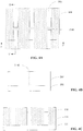
- FIGS. 2A to 7C are cross-sectional views illustrating intermediate stages of a semiconductor device in a manufacturing method according to an embodiment of the present invention.
- figures labelled NA are top or plan views of stages of the manufacturing method of a semiconductor device according to an embodiment of the present invention
- figures labelled NB are cross-sectional views taken along the line B-B' of the corresponding figures NA
- figures labelled NC are cross-sectional views taken along the line C-C' of the corresponding figures NA, where N is an integer ranging from 1 to 7.
- FIG. 1 A method for manufacturing a semiconductor device according to an embodiment of the present invention will be described below with reference to FIG. 1 and FIGS. 2A through 7C.
- FIG. 2A shows a plan view of a substrate structure according to an embodiment of the present invention.
- FIG. 2B is a cross-sectional view of the substrate structure shown in FIG. 2A taken along the line B-B', also referred to as the first direction.
- FIG. 2C is a cross-sectional view of the substrate structure shown in FIG. 2A taken along the line C-C', also referred to as the second direction.
- the substrate structure may include a substrate 201.
- Substrate 201 may be a silicon substrate, a substrate of a group III-V semiconductor material, an insulator-on-silicon (SOI) substrate, and the like.
- the substrate structure may also include one or more semiconductor fins 202 on substrate 201 and extending in the first direction (i.e., along the line B-B'), and a hardmask layer 203 on semiconductor fins 202.
- the first direction is the direction along the channel of a FinFET device.
- Semiconductor fins 202 may be formed of the same material as or of a different material than substrate 201.
- Hardmask layer 203 may include silicon oxide, silicon nitride, or silicon oxynitride. In one embodiment, hardmask layer 203 may include silicon nitride.
- the substrate structure may also include an isolation region 204 surrounding semiconductor fins 202.
- Isolation region 204 has an upper surface substantially flush with an upper surface of hardmask layer 203. As used herein, the term “substantially flush” means that the upper surfaces of the isolation region and the hardmask layer are flush or coplanar within an acceptable process standard deviation range.
- Isolation region 204 includes a first isolation region 214 and a second isolation region 224. First isolation region 214 is located on sides of semiconductor fins 202 in the first direction (i.e., the direction along the line B-B'), and the second isolation region 224 is located on sides of semiconductor fins 202 in the second direction different from the first direction (i.e., the direction along the line C-C').
- the second direction may be, for example, substantially perpendicular to the first direction, also referred to as the direction perpendicular to the channel.
- isolation region 204 may include a dielectric material, such as an oxide, a nitride, an oxynitride material.
- the isolation region between semiconductor fins 202 in the first direction is referred to as the first isolation region.
- the isolation region between semiconductor fins 202 in the second direction is referred to as the second isolation region.
- the substrate structure may be formed, for example, by providing an initial substrate, forming a patterned initial hardmask layer on the initial substrate, etching the initial substrate using the patterned initial hardmask layer as a mask to form a substrate, forming a first semiconductor fin on the substrate, and forming a first hardmask layer on the first semiconductor fin, cutting off the first semiconductor fin and the first hard mask layer using, e.g., a single diffusion break (SDB) process to form semiconductor fins and the hardmask layer on the semiconductor fins, and forming an isolation material (e.g., by deposition) and a spacer material. Thereafter, a planarization (e.g., CMP) process is performed on the isolation material to form the isolation region.
- SDB single diffusion break
- hardmask layer 203 is removed, as shown in FIGS. 3A, 3B, and 3C .
- hardmask layer 203 may be removed using a wet etching process. After removing hardmask layer 203, semiconductor fins 202 and a portion of first isolation region 214 above (higher than) the semiconductor fins 202 is exposed.
- step 106 an etch process is performed on the portion of first isolation region 214 that is above (higher than) semiconductor fins 202.
- first isolation region 214 that is above (higher than) semiconductor fin 202 is removed, so that a remaining first isolation region has an upper surface substantially flush with an upper surface of semiconductor fin 202.
- only a portion of first isolation region 214 that is above semiconductor fin 202 is removed, so that the upper surface of remaining first isolation region 214 is higher than the upper surface of semiconductor fin 202.
- first isolation region 214 above semiconductor fins 202 may be etched using a ribbon-like directional plasma etch process.
- the ribbon-like directional plasma etch process can etch a material in a certain direction while materials in other directions are basically not etched or etched only very little.
- first isolation region 214 disposed on a side of semiconductor fin 202 in the first direction is etched using the ribbon-like directional plasma etch process, and a portion of first isolation region 214 disposed on a side of semiconductor fin 202 in the second direction is not etched.
- a mask layer 501 is formed on semiconductor fins 202 and on a remaining first isolation region 214A, as shown in FIGS. 5A, 5B, and 5C .
- a mask material layer (not shown) may be formed on semiconductor fins 202, remaining first isolation region 214A, and second isolation region 224. Thereafter, in one embodiment, a planarization (e.g., a chemical mechanical polishing) process may be performed on the mask material layer to remove a portion of the mask material layer on second isolation region 224 so that a remaining mask material layer is substantially flush with second isolation region 224, the remaining mask material layer is a mask layer 501. Alternatively, in another embodiment, the mask material layer may be etched back to remove a portion of the mask material layer on second isolation region 224 so that a remaining mask material layer is substantially flush with second isolation region 224, the remaining mask material layer is mask layer 501.
- mask layer 501 may include silicon nitride, silicon oxide, or silicon oxynitride.
- second isolation region 224 is etched so that an upper surface of a remaining second isolation region 224A is lower than an upper surface of semiconductor fins 202, as shown in FIGS. 6A, 6B, and 6C .
- second isolation region 224 may be etched using a dry etch process.
- step 112 mask layer 501 is removed, as shown in FIGS. 7A, 7B, and 7C .
- mask layer 501 may be removed using a wet etch process.
- the upper surface of remaining first isolation region 214A is substantially flush with the upper surface of semiconductor fins 202, and the upper surface of remaining second isolation region 224A is lower than the upper surface of semiconductor fins 202. Further, as described above, the upper surface of remaining first isolation region 214A may be higher than the upper surface of semiconductor fins 202 in the case where a portion of first isolation region 214A that is above (higher than) semiconductor fins 202 is removed.
- first gate structure (not shown) may be formed on semiconductor fins 202, and a second gate structure (not shown) may be formed on remaining first isolation region 214A.
- the above-described manufacturing method provides an elevated isolation region, i.e., a first isolation region has an upper surface that is substantially flush with an upper surface of the semiconductor fins or higher than the upper surface of the semiconductor fins, that is, the height of the first isolation region has improved.
- a dummy gate structure corresponding to a subsequently formed second gate structure formed on the first isolation region will not form a bridge with the semiconductor fins even if there is some deviation in the dummy gate structure, thereby reducing leakage caused by the bridge formed between the dummy gate structure with the semiconductor fins and improving the reliability of the semiconductor device.
- Embodiments of the present invention also provide a semiconductor device.
- the semiconductor device includes a substrate 201, one or more semiconductor fins 202 on substrate 201 and extending in a first direction, and an isolation region surrounding semiconductor fins 202.
- the isolation region includes a first isolation region 214A and a second isolation region 224A.
- First isolation region 214A is disposed on a side of semiconductor fins 202 in the first direction and has an upper surface substantially flush with an upper surface of semiconductor fins 202, as shown in FIG. 7B , or the upper surface of first isolation region 214A is higher than the upper surface of semiconductor fins 202.
- Second isolation region 224A is disposed on a side of semiconductor fins 202 in a second direction different from the first direction and has an upper surface that is lower that the upper surface of semiconductor fins 202, as shown in FIG. 7C .
- the semiconductor device includes may also include a first gate structure (not shown) on semiconductor fins 202 and a second gate structure (not shown) on first isolation region 214A.
Landscapes
- Element Separation (AREA)
- Insulated Gate Type Field-Effect Transistor (AREA)
- Chemical & Material Sciences (AREA)
- Chemical Kinetics & Catalysis (AREA)
- General Chemical & Material Sciences (AREA)
Abstract


Description
- The present application claims priority to Chinese patent application No.
201611046394.X - The present invention relates to semiconductor technology, and more particularly to a semiconductor device and method for manufacturing the same.
- For improving the fin field effect transistor (FinFET) performance, distal ends of the fin of a FinFET is etched to form a recess, and a semiconductor material is epitaxially grown in the recess to introduce stress into the channel. A dummy gate structure may be formed on a shallow trench isolation (STI) to improve the morphology of the epitaxially grown semiconductor material.
- The present inventors have discovered that, because the upper surface of the STI region is lower than the upper surface of the fins, and as the features sizes of semiconductor devices decrease, the dummy gate structure on the STI region will be coupled to the fin if there is some slight deviation, i.e., a bridge is formed between the dummy gate and the fin, which may cause leakage and affect the reliability of a semiconductor device.
- It is an object of the present invention to provide a solution for solving the bridging problems when manufacturing a semiconductor device.
- The object is achieved by the features of the respective independent claims. Further embodiments and developments are defined in the dependent claims.
- A first aspect of the present invention provides a method for manufacturing a semiconductor device. The method includes providing a substrate structure having a substrate, one or more semiconductor fins extending in a first direction on the substrate, a hardmask layer on the semiconductor fins, and an isolation region surrounding the semiconductor fins and having an upper surface substantially flush with the hardmask layer, the isolation region including a first isolation region disposed on a side of the semiconductor fins in the first direction and a second isolation region disposed on a side of the semiconductor fins in a second direction different from the first direction. The method also includes removing the hardmask layer, etching a portion of the first isolation region above the semiconductor fins, forming a mask layer on the semiconductor fins and a remaining first isolation region, etching the second isolation region so that an upper surface of the remaining first isolation region is lower than an upper surface of the semiconductor fins, and removing the mask layer.
- Preferably, etching the portion of the first isolation region includes removing the portion of the first isolation region above the semiconductor fins, such that an upper surface of a remaining first isolation region is substantially flush with the upper surface of the semiconductor fins.
- Preferably, etching the portion of the first isolation region includes removing the portion of the first isolation region that is higher than the semiconductor fins so that an upper surface of a remaining first isolation region is higher than the upper surface of the semiconductor fins.
- Preferably, forming the mask layer on the semiconductor fins and the remaining first isolation region includes forming a mask material layer covering the semiconductor fins, the remaining first isolation region, and the second isolation region, and planarizing the mask material layer such that a remaining mask material layer is substantially flush with the second isolation region, the remaining mask material layer being the mask layer.
- Preferably, forming the mask layer on the semiconductor fins and the remaining first isolation region includes forming a mask material layer covering the semiconductor fins, the remaining first isolation region, and the second isolation region, and etching back the mask material layer so that a remaining mask material layer is substantially flush with the second isolation region, the remaining mask material layer being the mask layer.
- Preferably, removing the portion of the first isolation region above the semiconductor fins includes a ribbon-like directional plasma etch process.
- Preferably, removing the hardmask layer and removing the mask layer each include a wet etching process.
- Preferably, the hardmask layer, the isolation region, and the mask layer each include silicon oxide, silicon nitride, or silicon oxynitride.
- Preferably, the method further includes forming a first gate structure on the semiconductor fins, and forming a second gate structure on the remaining first isolation region.
- A second aspect of the present invention provides a semiconductor device, which includes a substrate, one or more semiconductor fins extending in a first direction on the substrate, and an isolation region surrounding the semiconductor fins. The isolation region includes a first isolation region and a second isolation region. The first isolation region is disposed on a side of the semiconductor fins in the first direction and has an upper surface substantially flush with an upper surface of the semiconductor fins, or the upper surface of the first isolation region is higher than the upper surface of the semiconductor fins. The second isolation region is disposed on a side of the semiconductor fins in a second direction different from the first direction and has an upper surface lower than an upper surface of the semiconductor fins.
- Preferably, the semiconductor device further includes a first gate structure on the semiconductor fins, and a second gate structure on the first isolation region.
- A device according to the second aspect of the present invention may be obtained by a method according to the first aspect of the present invention.
- The following detailed description together with the accompanying drawings will provide a better understanding of the nature and advantages of the present invention.
- Embodiments of the present invention are described with reference to the accompanying drawings. In the drawings, like reference numbers may indicate identical or functionally similar elements.
-
FIG. 1 is a simplified flowchart of a method for manufacturing a semiconductor device according to an embodiment of the present invention. -
FIGS. 2A to 7C are cross-sectional views illustrating intermediate stages of an interconnect structure in a manufacturing method according to an embodiment of the present invention. - Embodiments of the present invention now will be described more fully hereinafter with reference to the accompanying drawings. The invention may, however, be embodied in many different forms and should not be construed as limited to the embodiments set forth herein. Rather, these embodiments are provided so that this disclosure will be thorough and complete, and will fully convey the invention to those skilled in the art. The features may not be drawn to scale, some details may be exaggerated relative to other elements for clarity. In the drawings, like numbers refer to like elements throughout.
- It will be understood that when an element such as a layer, region or substrate is referred to as being "on" or extending "onto" another element, it can be directly on or extend directly onto the other element or intervening elements may also be present. In contrast, when an element is referred to as being "directly on" or extending "directly onto" another element, there are no intervening elements present. It will also be understood that when an element is referred to as being "connected" or "coupled" to another element, it can be directly connected or coupled to the other element or intervening elements may be present. In contrast, when an element is referred to as being "directly connected" or "directly coupled" to another element, there are no intervening elements present.
- Relative terms such as "below" or "above" or "upper" or "lower" or "horizontal" or "lateral" or "vertical" may be used herein to describe a relationship of one element, layer or region to another element, layer or region as illustrated in the figures. It will be understood that these terms are intended to encompass different orientations of the device in addition to the orientation depicted in the figures.
- The terminology used herein is for the purpose of describing particular embodiments only and is not intended to be limiting of the invention. As used herein, the singular forms "a", "an", and "the" are intended to include the plural forms as well, unless the context clearly indicates otherwise. It will be further understood that the terms "comprises", "comprising", "includes", and/or "including" when used herein, specify the presence of stated features, integers, steps, operations, elements, and/or components, but do not preclude the presence or addition of one or more other features, integers, steps, operations, elements, components, and/or groups thereof.
- Embodiments of the invention are described herein with reference to cross-sectional illustrations that are schematic illustrations of idealized embodiments (and intermediate structures) of the invention. The thickness of layers and regions in the drawings may be enlarged relative to other layers and regions for clarity. Additionally, variations from the shapes of the illustrations as a result, for example, of manufacturing techniques and/or tolerances, are to be expected. Thus, embodiments of the invention should not be construed as limited to the particular shapes of regions illustrated herein but are to include deviations in shapes that result, for example, from manufacturing. For example, an implanted region illustrated as a rectangle will, typically, have rounded or curved features and/or a gradient of implant concentration at its edges rather than a discrete change from implanted to non-implanted region. Likewise, a buried region formed by implantation may result in some implantation in the region between the buried region and the surface through which the implantation takes place. Thus, the regions illustrated in the figures are schematic in nature and their shapes are not intended to illustrate the actual shape of a region of a device and are not intended to limit the invention.
- The embodiments described and references in the disclosure to "one embodiment," "an embodiment," "an exemplary embodiment" indicate that the embodiments described may include a particular feature, structure, or characteristic. However, every embodiment may not necessary include the particular feature, structure or characteristic. As used throughout this disclosure, the terms "depositing" and "forming" are used interchangeably.
- It should be noted that like reference numerals are used to denote like elements, and once an element has been defined in a drawings, it will not be further described in other drawings.
- Embodiments of the present invention now will be described more fully hereinafter with reference to the accompanying drawings, in which embodiments of the invention are shown. This invention may, however, be embodied in many different forms and should not be construed as limited to the embodiments set forth herein.
- The present inventors discovered that the leakage problems can be solved or mitigated by increasing the height of the STI region, e.g., by raising the height of the STI region as high as that of the semiconductor fins. The inventors thus propose a novel method for forming a semiconductor device having a raised STI region.
-
FIG. 1 is a simplified flowchart of a method for manufacturing a semiconductor device according to an embodiment of the present invention.FIGS. 2A to 7C are cross-sectional views illustrating intermediate stages of a semiconductor device in a manufacturing method according to an embodiment of the present invention. In the following description, unless otherwise specified, figures labelled NA are top or plan views of stages of the manufacturing method of a semiconductor device according to an embodiment of the present invention, figures labelled NB are cross-sectional views taken along the line B-B' of the corresponding figures NA, and figures labelled NC are cross-sectional views taken along the line C-C' of the corresponding figures NA, where N is an integer ranging from 1 to 7. - A method for manufacturing a semiconductor device according to an embodiment of the present invention will be described below with reference to
FIG. 1 andFIGS. 2A through 7C. - Referring to
FIG. 1 , a substrate structure is provided atstep 102.FIG. 2A shows a plan view of a substrate structure according to an embodiment of the present invention.FIG. 2B is a cross-sectional view of the substrate structure shown inFIG. 2A taken along the line B-B', also referred to as the first direction.FIG. 2C is a cross-sectional view of the substrate structure shown inFIG. 2A taken along the line C-C', also referred to as the second direction. - Referring to
FIGS. 2A, 2B, and 2C , the substrate structure may include asubstrate 201.Substrate 201 may be a silicon substrate, a substrate of a group III-V semiconductor material, an insulator-on-silicon (SOI) substrate, and the like. - The substrate structure may also include one or
more semiconductor fins 202 onsubstrate 201 and extending in the first direction (i.e., along the line B-B'), and ahardmask layer 203 onsemiconductor fins 202. The first direction is the direction along the channel of a FinFET device.Semiconductor fins 202 may be formed of the same material as or of a different material thansubstrate 201.Hardmask layer 203 may include silicon oxide, silicon nitride, or silicon oxynitride. In one embodiment,hardmask layer 203 may include silicon nitride. - The substrate structure may also include an
isolation region 204 surroundingsemiconductor fins 202.Isolation region 204 has an upper surface substantially flush with an upper surface ofhardmask layer 203. As used herein, the term "substantially flush" means that the upper surfaces of the isolation region and the hardmask layer are flush or coplanar within an acceptable process standard deviation range.Isolation region 204 includes afirst isolation region 214 and asecond isolation region 224.First isolation region 214 is located on sides ofsemiconductor fins 202 in the first direction (i.e., the direction along the line B-B'), and thesecond isolation region 224 is located on sides ofsemiconductor fins 202 in the second direction different from the first direction (i.e., the direction along the line C-C'). The second direction may be, for example, substantially perpendicular to the first direction, also referred to as the direction perpendicular to the channel. In one embodiment,isolation region 204 may include a dielectric material, such as an oxide, a nitride, an oxynitride material. - It will be appreciated that in the case where the substrate structure includes
multiple semiconductor fins 202 extending in the first direction, the isolation region betweensemiconductor fins 202 in the first direction is referred to as the first isolation region. In the case where the substrate structure includesmultiple semiconductor fins 202 extending in the second direction, the isolation region betweensemiconductor fins 202 in the second direction is referred to as the second isolation region. - The substrate structure may be formed, for example, by providing an initial substrate, forming a patterned initial hardmask layer on the initial substrate, etching the initial substrate using the patterned initial hardmask layer as a mask to form a substrate, forming a first semiconductor fin on the substrate, and forming a first hardmask layer on the first semiconductor fin, cutting off the first semiconductor fin and the first hard mask layer using, e.g., a single diffusion break (SDB) process to form semiconductor fins and the hardmask layer on the semiconductor fins, and forming an isolation material (e.g., by deposition) and a spacer material. Thereafter, a planarization (e.g., CMP) process is performed on the isolation material to form the isolation region.
- Referring back to
FIG. 1 , instep 104,hardmask layer 203 is removed, as shown inFIGS. 3A, 3B, and 3C . For example,hardmask layer 203 may be removed using a wet etching process. After removinghardmask layer 203,semiconductor fins 202 and a portion offirst isolation region 214 above (higher than) thesemiconductor fins 202 is exposed. - Next, in
step 106, an etch process is performed on the portion offirst isolation region 214 that is above (higher than)semiconductor fins 202. - In one embodiment, referring to
FIGS. 4A, 4B, and 4C , the entire portion offirst isolation region 214 that is above (higher than)semiconductor fin 202 is removed, so that a remaining first isolation region has an upper surface substantially flush with an upper surface ofsemiconductor fin 202. In another embodiment, only a portion offirst isolation region 214 that is abovesemiconductor fin 202 is removed, so that the upper surface of remainingfirst isolation region 214 is higher than the upper surface ofsemiconductor fin 202. - In one embodiment, a portion of
first isolation region 214 abovesemiconductor fins 202 may be etched using a ribbon-like directional plasma etch process. The ribbon-like directional plasma etch process can etch a material in a certain direction while materials in other directions are basically not etched or etched only very little. Thus, only a portion offirst isolation region 214 disposed on a side ofsemiconductor fin 202 in the first direction is etched using the ribbon-like directional plasma etch process, and a portion offirst isolation region 214 disposed on a side ofsemiconductor fin 202 in the second direction is not etched. - Next, in
step 108, amask layer 501 is formed onsemiconductor fins 202 and on a remainingfirst isolation region 214A, as shown inFIGS. 5A, 5B, and 5C . - In one embodiment, a mask material layer (not shown) may be formed on
semiconductor fins 202, remainingfirst isolation region 214A, andsecond isolation region 224. Thereafter, in one embodiment, a planarization (e.g., a chemical mechanical polishing) process may be performed on the mask material layer to remove a portion of the mask material layer onsecond isolation region 224 so that a remaining mask material layer is substantially flush withsecond isolation region 224, the remaining mask material layer is amask layer 501. Alternatively, in another embodiment, the mask material layer may be etched back to remove a portion of the mask material layer onsecond isolation region 224 so that a remaining mask material layer is substantially flush withsecond isolation region 224, the remaining mask material layer ismask layer 501. In an exemplary embodiment,mask layer 501 may include silicon nitride, silicon oxide, or silicon oxynitride. - Next, in
step 110,second isolation region 224 is etched so that an upper surface of a remainingsecond isolation region 224A is lower than an upper surface ofsemiconductor fins 202, as shown inFIGS. 6A, 6B, and 6C . For example,second isolation region 224 may be etched using a dry etch process. - Next, in
step 112,mask layer 501 is removed, as shown inFIGS. 7A, 7B, and 7C . For example,mask layer 501 may be removed using a wet etch process. - Referring to
FIGS. 7B and 7C , the upper surface of remainingfirst isolation region 214A is substantially flush with the upper surface ofsemiconductor fins 202, and the upper surface of remainingsecond isolation region 224A is lower than the upper surface ofsemiconductor fins 202. Further, as described above, the upper surface of remainingfirst isolation region 214A may be higher than the upper surface ofsemiconductor fins 202 in the case where a portion offirst isolation region 214A that is above (higher than)semiconductor fins 202 is removed. - Thereafter, a first gate structure (not shown) may be formed on
semiconductor fins 202, and a second gate structure (not shown) may be formed on remainingfirst isolation region 214A. - The above-described manufacturing method provides an elevated isolation region, i.e., a first isolation region has an upper surface that is substantially flush with an upper surface of the semiconductor fins or higher than the upper surface of the semiconductor fins, that is, the height of the first isolation region has improved. Thus, a dummy gate structure (corresponding to a subsequently formed second gate structure) formed on the first isolation region will not form a bridge with the semiconductor fins even if there is some deviation in the dummy gate structure, thereby reducing leakage caused by the bridge formed between the dummy gate structure with the semiconductor fins and improving the reliability of the semiconductor device.
- Embodiments of the present invention also provide a semiconductor device. Referring to
FIGS. 7A, 7B, and 7C , the semiconductor device includes asubstrate 201, one ormore semiconductor fins 202 onsubstrate 201 and extending in a first direction, and an isolation region surroundingsemiconductor fins 202. The isolation region includes afirst isolation region 214A and asecond isolation region 224A.First isolation region 214A is disposed on a side ofsemiconductor fins 202 in the first direction and has an upper surface substantially flush with an upper surface ofsemiconductor fins 202, as shown inFIG. 7B , or the upper surface offirst isolation region 214A is higher than the upper surface ofsemiconductor fins 202.Second isolation region 224A is disposed on a side ofsemiconductor fins 202 in a second direction different from the first direction and has an upper surface that is lower that the upper surface ofsemiconductor fins 202, as shown inFIG. 7C . - In one embodiment, the semiconductor device includes may also include a first gate structure (not shown) on
semiconductor fins 202 and a second gate structure (not shown) onfirst isolation region 214A.
Claims (12)
- A method for manufacturing a semiconductor device, the method comprising:providing a substrate structure including a substrate, one or more semiconductor fins extending in a first direction on the substrate, a hardmask layer on the semiconductor fins, and an isolation region surrounding the semiconductor fins and having an upper surface substantially flush with the hardmask layer, the isolation region including a first isolation region disposed on a side of the semiconductor fins in the first direction and a second isolation region disposed on a side of the semiconductor fins in a second direction different from the first direction;removing the hardmask layer;etching a portion of the first isolation region above the semiconductor fins;forming a mask layer on the semiconductor fins and a remaining first isolation region;etching the second isolation region so that an upper surface of the remaining first isolation region is lower than an upper surface of the semiconductor fins; andremoving the mask layer.
- The method of claim 1, wherein etching the portion of the first isolation region comprises:removing the portion of the first isolation region above the semiconductor fins so that an upper surface of a remaining first isolation region is substantially flush with the upper surface of the semiconductor fins.
- The method of claim 1, wherein etching the portion of the first isolation region comprises:removing the portion of the first isolation region that is higher than the semiconductor fins so that an upper surface of a remaining first isolation region is higher than the upper surface of the semiconductor fins.
- The method of any one of the claims 1-3, wherein forming the mask layer on the semiconductor fins and the remaining first isolation region comprises:forming a mask material layer covering the semiconductor fins, the remaining first isolation region, and the second isolation region;planarizing the mask material layer so that a remaining mask material layer is substantially flush with the second isolation region, the remaining mask material layer being the mask layer.
- The method of any one of the claims 1-3, wherein forming the mask layer on the semiconductor fins and the remaining first isolation region comprises:forming a mask material layer covering the semiconductor fins, the remaining first isolation region, and the second isolation region;etching back the mask material layer so that a remaining mask material layer is substantially flush with the second isolation region, the remaining mask material layer being the mask layer.
- The method of any one of the claims 1-5, wherein removing the portion of the first isolation region above the semiconductor fins comprises a ribbon-like directional plasma etch process.
- The method of any one of the claims 1-6, wherein removing the hardmask layer comprises a wet etching process.
- The method of any one of the claims 1-7, wherein removing the mask layer comprises a wet etching process.
- The method of any one of the claims 1-8, wherein the hardmask layer, the isolation region, and the mask layer each comprise silicon oxide, silicon nitride, or silicon oxynitride.
- The method of any one of the claims 1-9, further comprising:forming a first gate structure on the semiconductor fins; andforming a second gate structure on the remaining first isolation region.
- A semiconductor device, comprising:a substrate;one or more semiconductor fins extending in a first direction on the substrate; andan isolation region surrounding the semiconductor fins and including a first isolation region and a second isolation region, wherein the first isolation region is disposed on a side of the semiconductor fins in the first direction and has an upper surface substantially flush with an upper surface of the semiconductor fins, or the upper surface of the first isolation region is higher than the upper surface of the semiconductor fins, anda second isolation region is disposed on a side of the semiconductor fins in a second direction different from the first direction and has an upper surface lower than an upper surface of the semiconductor fins.
- The semiconductor device of claim 11, further comprising:a first gate structure on the semiconductor fins; anda second gate structure on the first isolation region.
Applications Claiming Priority (1)
| Application Number | Priority Date | Filing Date | Title |
|---|---|---|---|
| CN201611046394.XA CN108091611B (en) | 2016-11-23 | 2016-11-23 | Semiconductor device and method of manufacturing the same |
Publications (1)
| Publication Number | Publication Date |
|---|---|
| EP3327789A1 true EP3327789A1 (en) | 2018-05-30 |
Family
ID=60452426
Family Applications (1)
| Application Number | Title | Priority Date | Filing Date |
|---|---|---|---|
| EP17202998.5A Withdrawn EP3327789A1 (en) | 2016-11-23 | 2017-11-22 | Fin cut process and fin structure |
Country Status (3)
| Country | Link |
|---|---|
| US (1) | US10325813B2 (en) |
| EP (1) | EP3327789A1 (en) |
| CN (1) | CN108091611B (en) |
Families Citing this family (4)
| Publication number | Priority date | Publication date | Assignee | Title |
|---|---|---|---|---|
| CN111640665B (en) * | 2019-03-01 | 2023-05-26 | 中芯国际集成电路制造(上海)有限公司 | Semiconductor device and method of forming the same |
| US10985161B2 (en) | 2019-05-31 | 2021-04-20 | International Business Machines Corporation | Single diffusion break isolation for gate-all-around field-effect transistor devices |
| US11688650B2 (en) * | 2019-07-05 | 2023-06-27 | Tokyo Electron Limited | Etching method and substrate processing apparatus |
| US20250191966A1 (en) * | 2023-12-07 | 2025-06-12 | International Business Machines Corporation | Lowering gate aspect ratio on sti region |
Citations (5)
| Publication number | Priority date | Publication date | Assignee | Title |
|---|---|---|---|---|
| US20070111455A1 (en) * | 2005-11-14 | 2007-05-17 | Samsung Electronics Co., Ltd. | Fabrication of local damascene finFETs using contact type nitride damascene mask |
| US20140117454A1 (en) * | 2012-10-26 | 2014-05-01 | Taiwan Semiconductor Manufacturing Company, Ltd. | FinFET with Dummy Gate on Non-Recessed Shallow Trench Isolation (STI) |
| US20140264572A1 (en) * | 2013-03-15 | 2014-09-18 | Sung-min Kim | Methods of forming semiconductor devices using hard mask layers |
| US20150162247A1 (en) * | 2013-12-11 | 2015-06-11 | Samsung Electronics Co., Ltd. | Semiconductor device, electronic device including the same and manufacturing methods thereof |
| US20160225848A1 (en) * | 2015-01-30 | 2016-08-04 | Globalfoundries Inc. | Process for single diffusion break with simplfied process |
Family Cites Families (3)
| Publication number | Priority date | Publication date | Assignee | Title |
|---|---|---|---|---|
| KR102085525B1 (en) * | 2013-11-27 | 2020-03-09 | 삼성전자 주식회사 | Semiconductor device and method for fabricating the same |
| US9368496B1 (en) * | 2015-01-30 | 2016-06-14 | Globalfoundries Inc. | Method for uniform recess depth and fill in single diffusion break for fin-type process and resulting devices |
| US10061199B2 (en) * | 2015-06-24 | 2018-08-28 | Tokyo Electron Limited | Methods of forming a mask for substrate patterning |
-
2016
- 2016-11-23 CN CN201611046394.XA patent/CN108091611B/en active Active
-
2017
- 2017-10-09 US US15/728,204 patent/US10325813B2/en active Active
- 2017-11-22 EP EP17202998.5A patent/EP3327789A1/en not_active Withdrawn
Patent Citations (5)
| Publication number | Priority date | Publication date | Assignee | Title |
|---|---|---|---|---|
| US20070111455A1 (en) * | 2005-11-14 | 2007-05-17 | Samsung Electronics Co., Ltd. | Fabrication of local damascene finFETs using contact type nitride damascene mask |
| US20140117454A1 (en) * | 2012-10-26 | 2014-05-01 | Taiwan Semiconductor Manufacturing Company, Ltd. | FinFET with Dummy Gate on Non-Recessed Shallow Trench Isolation (STI) |
| US20140264572A1 (en) * | 2013-03-15 | 2014-09-18 | Sung-min Kim | Methods of forming semiconductor devices using hard mask layers |
| US20150162247A1 (en) * | 2013-12-11 | 2015-06-11 | Samsung Electronics Co., Ltd. | Semiconductor device, electronic device including the same and manufacturing methods thereof |
| US20160225848A1 (en) * | 2015-01-30 | 2016-08-04 | Globalfoundries Inc. | Process for single diffusion break with simplfied process |
Non-Patent Citations (1)
| Title |
|---|
| RUFFELL SIMON ET AL: "Directed ribbon-beam capability for novel etching applications", JOURNAL OF VACUUM SCIENCE & TECHNOLOGY B: MICROELECTRONICS AND NANOMETER STRUCTURES, AMERICAN INSTITUTE OF PHYSICS, 2 HUNTINGTON QUADRANGLE, MELVILLE, NY 11747, vol. 33, no. 6, 1 January 1901 (1901-01-01), XP012200946, ISSN: 2166-2746, [retrieved on 19010101], DOI: 10.1116/1.4932161 * |
Also Published As
| Publication number | Publication date |
|---|---|
| CN108091611A (en) | 2018-05-29 |
| US10325813B2 (en) | 2019-06-18 |
| CN108091611B (en) | 2020-11-13 |
| US20180144986A1 (en) | 2018-05-24 |
Similar Documents
| Publication | Publication Date | Title |
|---|---|---|
| CN103928335B (en) | Semiconductor device and manufacturing method thereof | |
| US10930765B2 (en) | Method of manufacturing FinFET device with non-recessed STI | |
| US11575010B2 (en) | Semiconductor device and manufacturing method thereof | |
| US10748899B2 (en) | Epitaxial source and drain structures for high voltage devices | |
| US10325813B2 (en) | Fin cut process and fin structure | |
| EP3316286A1 (en) | Dummy gate structures and manufacturing method thereof | |
| US9082717B2 (en) | Isolation region, semiconductor device and methods for forming the same | |
| TWI546892B (en) | Semiconductor device and method of forming same | |
| EP3264471A1 (en) | Improved epi integrality on source/drain region of finfet | |
| US9633893B2 (en) | Method to protect against contact related shorts on UTBB | |
| EP3319128A1 (en) | Method to improve channel stop implantation | |
| JP2010171144A (en) | Semiconductor device | |
| EP3176816A1 (en) | Well implantation process for finfet device | |
| US10008495B2 (en) | Method for forming FinFET device | |
| CN103578987B (en) | Semiconductor device and manufacturing method thereof | |
| US10600890B2 (en) | Contact to metal gate isolation structure | |
| CN109427907B (en) | Semiconductor device and manufacturing method thereof | |
| KR101051809B1 (en) | High voltage device and manufacturing method thereof | |
| KR100613370B1 (en) | Semiconductor device and manufacturing method thereof | |
| KR100490846B1 (en) | Semiconductor device and fabrication method thereof | |
| CN117727686A (en) | A shallow trench isolation structure and preparation method | |
| CN116469772A (en) | Method for preparing semiconductor structure and semiconductor structure | |
| KR100373710B1 (en) | manufacturing method of shallow trench isolation of semiconductor devices | |
| KR100323720B1 (en) | Elevated semiconductor layer and method for forming the same | |
| KR20050117330A (en) | Method of making isolation layer of semiconductor device |
Legal Events
| Date | Code | Title | Description |
|---|---|---|---|
| PUAI | Public reference made under article 153(3) epc to a published international application that has entered the european phase |
Free format text: ORIGINAL CODE: 0009012 |
|
| STAA | Information on the status of an ep patent application or granted ep patent |
Free format text: STATUS: THE APPLICATION HAS BEEN PUBLISHED |
|
| AK | Designated contracting states |
Kind code of ref document: A1 Designated state(s): AL AT BE BG CH CY CZ DE DK EE ES FI FR GB GR HR HU IE IS IT LI LT LU LV MC MK MT NL NO PL PT RO RS SE SI SK SM TR |
|
| AX | Request for extension of the european patent |
Extension state: BA ME |
|
| STAA | Information on the status of an ep patent application or granted ep patent |
Free format text: STATUS: REQUEST FOR EXAMINATION WAS MADE |
|
| 17P | Request for examination filed |
Effective date: 20180920 |
|
| RBV | Designated contracting states (corrected) |
Designated state(s): AL AT BE BG CH CY CZ DE DK EE ES FI FR GB GR HR HU IE IS IT LI LT LU LV MC MK MT NL NO PL PT RO RS SE SI SK SM TR |
|
| RAP1 | Party data changed (applicant data changed or rights of an application transferred) |
Owner name: SEMICONDUCTOR MANUFACTURING INTERNATIONAL (BEIJING Owner name: SEMICONDUCTOR MANUFACTURING INTERNATIONAL (SHANGHA |
|
| STAA | Information on the status of an ep patent application or granted ep patent |
Free format text: STATUS: EXAMINATION IS IN PROGRESS |
|
| 17Q | First examination report despatched |
Effective date: 20200819 |
|
| STAA | Information on the status of an ep patent application or granted ep patent |
Free format text: STATUS: THE APPLICATION IS DEEMED TO BE WITHDRAWN |
|
| 18D | Application deemed to be withdrawn |
Effective date: 20210112 |