EP3326061B1 - Simd sliding window operation - Google Patents
Simd sliding window operation Download PDFInfo
- Publication number
- EP3326061B1 EP3326061B1 EP16742134.6A EP16742134A EP3326061B1 EP 3326061 B1 EP3326061 B1 EP 3326061B1 EP 16742134 A EP16742134 A EP 16742134A EP 3326061 B1 EP3326061 B1 EP 3326061B1
- Authority
- EP
- European Patent Office
- Prior art keywords
- lane
- register
- input data
- data element
- simd
- Prior art date
- Legal status (The legal status is an assumption and is not a legal conclusion. Google has not performed a legal analysis and makes no representation as to the accuracy of the status listed.)
- Active
Links
Images


Classifications
-
- G—PHYSICS
- G06—COMPUTING OR CALCULATING; COUNTING
- G06F—ELECTRIC DIGITAL DATA PROCESSING
- G06F9/00—Arrangements for program control, e.g. control units
- G06F9/06—Arrangements for program control, e.g. control units using stored programs, i.e. using an internal store of processing equipment to receive or retain programs
- G06F9/30—Arrangements for executing machine instructions, e.g. instruction decode
- G06F9/30003—Arrangements for executing specific machine instructions
- G06F9/30007—Arrangements for executing specific machine instructions to perform operations on data operands
- G06F9/3001—Arithmetic instructions
-
- G—PHYSICS
- G06—COMPUTING OR CALCULATING; COUNTING
- G06F—ELECTRIC DIGITAL DATA PROCESSING
- G06F15/00—Digital computers in general; Data processing equipment in general
- G06F15/76—Architectures of general purpose stored program computers
- G06F15/82—Architectures of general purpose stored program computers data or demand driven
-
- G—PHYSICS
- G06—COMPUTING OR CALCULATING; COUNTING
- G06F—ELECTRIC DIGITAL DATA PROCESSING
- G06F9/00—Arrangements for program control, e.g. control units
- G06F9/06—Arrangements for program control, e.g. control units using stored programs, i.e. using an internal store of processing equipment to receive or retain programs
- G06F9/30—Arrangements for executing machine instructions, e.g. instruction decode
- G06F9/30003—Arrangements for executing specific machine instructions
- G06F9/30007—Arrangements for executing specific machine instructions to perform operations on data operands
- G06F9/30032—Movement instructions, e.g. MOVE, SHIFT, ROTATE, SHUFFLE
-
- G—PHYSICS
- G06—COMPUTING OR CALCULATING; COUNTING
- G06F—ELECTRIC DIGITAL DATA PROCESSING
- G06F9/00—Arrangements for program control, e.g. control units
- G06F9/06—Arrangements for program control, e.g. control units using stored programs, i.e. using an internal store of processing equipment to receive or retain programs
- G06F9/30—Arrangements for executing machine instructions, e.g. instruction decode
- G06F9/30003—Arrangements for executing specific machine instructions
- G06F9/30007—Arrangements for executing specific machine instructions to perform operations on data operands
- G06F9/30036—Instructions to perform operations on packed data, e.g. vector, tile or matrix operations
-
- G—PHYSICS
- G06—COMPUTING OR CALCULATING; COUNTING
- G06F—ELECTRIC DIGITAL DATA PROCESSING
- G06F9/00—Arrangements for program control, e.g. control units
- G06F9/06—Arrangements for program control, e.g. control units using stored programs, i.e. using an internal store of processing equipment to receive or retain programs
- G06F9/30—Arrangements for executing machine instructions, e.g. instruction decode
- G06F9/30098—Register arrangements
- G06F9/3012—Organisation of register space, e.g. banked or distributed register file
- G06F9/30134—Register stacks; shift registers
-
- G—PHYSICS
- G06—COMPUTING OR CALCULATING; COUNTING
- G06F—ELECTRIC DIGITAL DATA PROCESSING
- G06F9/00—Arrangements for program control, e.g. control units
- G06F9/06—Arrangements for program control, e.g. control units using stored programs, i.e. using an internal store of processing equipment to receive or retain programs
- G06F9/30—Arrangements for executing machine instructions, e.g. instruction decode
- G06F9/38—Concurrent instruction execution, e.g. pipeline or look ahead
- G06F9/3885—Concurrent instruction execution, e.g. pipeline or look ahead using a plurality of independent parallel functional units
- G06F9/3887—Concurrent instruction execution, e.g. pipeline or look ahead using a plurality of independent parallel functional units controlled by a single instruction for multiple data lanes [SIMD]
-
- G—PHYSICS
- G06—COMPUTING OR CALCULATING; COUNTING
- G06F—ELECTRIC DIGITAL DATA PROCESSING
- G06F15/00—Digital computers in general; Data processing equipment in general
- G06F15/76—Architectures of general purpose stored program computers
- G06F15/80—Architectures of general purpose stored program computers comprising an array of processing units with common control, e.g. single instruction multiple data processors
- G06F15/8007—Architectures of general purpose stored program computers comprising an array of processing units with common control, e.g. single instruction multiple data processors single instruction multiple data [SIMD] multiprocessors
-
- G—PHYSICS
- G06—COMPUTING OR CALCULATING; COUNTING
- G06F—ELECTRIC DIGITAL DATA PROCESSING
- G06F9/00—Arrangements for program control, e.g. control units
- G06F9/06—Arrangements for program control, e.g. control units using stored programs, i.e. using an internal store of processing equipment to receive or retain programs
- G06F9/30—Arrangements for executing machine instructions, e.g. instruction decode
- G06F9/30003—Arrangements for executing specific machine instructions
- G06F9/30007—Arrangements for executing specific machine instructions to perform operations on data operands
- G06F9/30021—Compare instructions, e.g. Greater-Than, Equal-To, MINMAX
-
- G—PHYSICS
- G06—COMPUTING OR CALCULATING; COUNTING
- G06F—ELECTRIC DIGITAL DATA PROCESSING
- G06F9/00—Arrangements for program control, e.g. control units
- G06F9/06—Arrangements for program control, e.g. control units using stored programs, i.e. using an internal store of processing equipment to receive or retain programs
- G06F9/30—Arrangements for executing machine instructions, e.g. instruction decode
- G06F9/30003—Arrangements for executing specific machine instructions
- G06F9/30007—Arrangements for executing specific machine instructions to perform operations on data operands
- G06F9/30029—Logical and Boolean instructions, e.g. XOR, NOT
-
- G—PHYSICS
- G06—COMPUTING OR CALCULATING; COUNTING
- G06F—ELECTRIC DIGITAL DATA PROCESSING
- G06F9/00—Arrangements for program control, e.g. control units
- G06F9/06—Arrangements for program control, e.g. control units using stored programs, i.e. using an internal store of processing equipment to receive or retain programs
- G06F9/30—Arrangements for executing machine instructions, e.g. instruction decode
- G06F9/30098—Register arrangements
- G06F9/30105—Register structure
- G06F9/30112—Register structure comprising data of variable length
Definitions
- the present disclosure is generally related to sliding window operations for a single-instruction-multiple-data (SIMD) architecture. More specifically, the present disclosure is related to reducing an amount of shifts and registers associated with performing the sliding window operations.
- SIMD single-instruction-multiple-data
- wireless telephones such as mobile and smart phones, tablets and laptop computers that are small, lightweight, and easily carried by users.
- These devices can communicate voice and data packets over wireless networks.
- many such devices incorporate additional functionality such as a digital still camera, a digital video camera, a digital recorder, and an audio file player.
- such devices can process executable instructions, including software applications, such as a web browser application, that can be used to access the Internet. As such, these devices can include significant computing capabilities.
- a conventional convolution function may use a "sliding window" to process an input data stream.
- a sliding window of a portion of data elements from the input data stream may be used to generate a first output that is a function (e.g., a sum of products) of each data element in the sliding window.
- the sliding window is shifted and the next output is determined as a function of each data element in the shifted sliding window.
- a relatively large number of registers and shifts may be used to perform convolution functions using a conventional sliding window instruction.
- a single-instruction-multiple-data (SIMD) architecture may execute a conventional sliding window instruction using a four data input "lane.”
- the lane may perform a convolution function on four data inputs (e.g., a sliding window width of "4") from a register to produce an output.
- the data elements may be shifted by one location in a second register and the lane may perform a convolution function on the data elements in the second register.
- United States Patent No. 6,009,505 relates to a system and method for routing one operand to arithmetic logic units from fixed register slots and another operand from any register slot.
- the present invention relates to an apparatus and a method as defined in the appended claims.
- Systems and methods for reducing shifts and registers for performing sliding window operations are disclosed.
- techniques for performing sliding window operations within a single SIMD lane by referencing multiple registers that include data for operations are disclosed.
- a sliding window operation references a first register and a second register.
- a SIMD lane may reference the first register and the second register to perform sliding window operations on data in the first and second registers.
- a portion of the first register in the SIMD lane may store four data elements (e.g., data element “0”, data element “1”, data element “2”, and data element “3") of an input data stream
- a portion of the second register in the SIMD lane may store the next four data elements (e.g., data element "4", data element "5", data element "6", and data element "7") of the input data stream.
- the corresponding portion of the second register may include shifted data of the input data stream.
- the SIMD lane references the two registers to perform up to five sliding window operations.
- a SIMD architecture may multiplex data in the registers to perform the sliding window operations.
- the first SIMD lane may perform a first sliding operation using the first four data elements in the first register (e.g., data element "0", data element "1", data element "2", and data element "3"), a second sliding window operation using data elements "1, 2, and 3" of the first register and data element "4" of the second register, a third sliding window operation using data elements "2 and 3" of the first register and data elements "4 and 5" of the second register, a fourth sliding window operation using data element “3" of the first register and data elements "4, 5, and 6" of the second register, etc.
- an apparatus in a particular aspect, includes a first register having a lane storing first input data elements; a second register having a lane storing second input data elements, wherein a width N of the lane of the second register is equal to a width N of the lane of the first register and characterised in that the first input data elements include N data elements of an input data stream and the second input data elements include a next N data elements of the input data stream, such that the second input data elements are shifted by N relative to the first input data elements; and a single-instruction-multiple-data, SIMD, lane having a lane width N equal to the width of the lane of the first register, wherein the SIMD lane is configured to perform a plurality of sliding window operations on the first input data elements in the lane of the first register and the second input data elements in the lane of the second register, wherein performing each sliding window operation includes determining a result based on a first position input data element selected from a first input data element stored in a first position of the
- a method in another particular aspect, includes storing first input data elements in a lane of a first register; storing second input data elements in a lane of a second register, wherein a width of the lane of the second register is equal to a width of the lane of the first register, characterised in that the first input data elements include N data elements of an input data stream and the second input data elements include a next N data elements of the input data stream, such that the second input data elements are shifted by N relative to the first input data elements; and performing a plurality of sliding window operations on the first input data elements in the lane of the first register and the second input data elements in the lane of the second register using a single-instruction-multiple-data, SIMD, lane having a lane width N equal to the width of the lane of the first register, wherein performing each sliding window operation includes determining a result based on a first position input data element selected from a first input data element stored in a first position of the first register and a second input data element stored
- SIMD lane may perform sliding window operations using fewer registers and shifts than a conventional SIMD architecture.
- the system performs the sliding window operations within a single-instruction-multiple-data (SIMD) lane by referencing multiple registers that include data for the operations.
- SIMD single-instruction-multiple-data
- the system includes a SIMD architecture 102 (e.g., convolutional function hardware and/or sliding window hardware).
- Input data 104 is provided to the SIMD architecture 102. As described below, particular portions of the input data 104 may be shifted and stored in certain register positions to enable sliding window operations to be performed according to the techniques described herein.
- the input data 104 may include sixty-four data elements (e.g., data element "0” to data element “63”). In alternative implementations, the input data 104 may include additional (or fewer data elements).
- the input data 104 includes first input data elements 106 and second input data elements 108.
- the first input data elements 106 may include data element “0", data element "1", data element "2", and data element "3".
- the second input data elements 108 may include data element "4", data element "5", data element "6", and data element "7".
- the input data 104 may also include third input data elements (e.g., data element “8” through data element “11"), fourth input data elements (e.g., data element “12” through data element “15”), fifth input data elements (e.g., data element "16” through data element “19”), etc.
- third input data elements e.g., data element "8” through data element “11”
- fourth input data elements e.g., data element "12” through data element “15”
- fifth input data elements e.g., data element "16” through data element “19
- the SIMD architecture 102 may be configured to apply a convolution function to the input data 104 to generate output data 110.
- the SIMD architecture 102 applies a "sliding window" function to data elements in the input data 104 to generate the output data 110.
- Each output data element of the output data 110 may be a function (e.g., a sum of products) of the input data elements in the sliding window.
- a first output data element of the output data 110 may be a sum of products of the first input data elements 106.
- the first output data element of the output data 110 may be a function of data element "0", data element "1", data element "2", and data element "3".
- the second output data element of the output data 110 may be a function of data element "1", data element "2", data element "3", and data element "4".
- the SIMD architecture 102 may include a first SIMD lane 122, a second SIMD lane 124, a third SIMD lane 126, and a fourth SIMD lane 128. Although four SIMD lanes are depicted in FIG. 1 , in alternative implementations, additional (or fewer) SIMD lanes may be included in the SIMD architecture 102. As described below, each SIMD lane 122-128 is configured to perform sliding window operations on input data elements within the corresponding SIMD lane 122-128.
- the system also includes a first register 130 and a second register 140.
- Each register 130, 140 stores input data elements of the input data 104.
- the first register 130 may include a first lane 132, a second lane 134, a third lane 136, and a fourth lane 138.
- each lane 132-138 of the first register 130 may have a width of four.
- each lane 132-138 of the first register 130 may be allocated to store four data elements.
- each lane 132-138 of the first register 130 may be operable to store four input data elements of the input data 104.
- the first lane 132 of the first register 130 may store the first input data elements 106 (e.g., data element “0” through data element “3") of the input data 104
- the second lane 134 of the first register 130 may store the second input data elements 108 (e.g., data element "4" through data element “7") of the input data 104
- the third lane 136 of the first register 130 may store the third input data elements (e.g., data element "8” through data element "11") of the input data 104
- the fourth lane 138 of the first register 130 may store the fourth input data elements (e.g. data element "12” through data element "15") of the input data 104.
- each lane 132-138 of the first register 130 is equal to a lane width of a corresponding SIMD lane 122-128.
- the lane width of the first SIMD lane 122 is equal to the width of the first lane 132 of the first register 130
- the lane width of the second SIMD lane 124 is equal to the width of the second lane 134 of the first register 130
- the lane width of the third SIMD lane 126 is equal to the width of the third lane 136 of the first register 130
- the lane width of the fourth SIMD lane 128 is equal to the width of the fourth lane 138 of the first register 130.
- the second register 140 may include a first lane 142, a second lane 144, a third lane 146, and a fourth lane 148.
- each lane 142-148 of the second register 140 may also have a width of four.
- each lane 142-148 of the second register 140 may be operable to store four input data elements of the input data 104.
- the input data elements stored in the corresponding lanes 142-148 of the second register 140 may be shifted by the lane width (e.g., shifted by four).
- the first lane 142 of the second register 140 may store the second input data elements 108 (e.g., data element "4" through data element "7") of the input data 104
- the second lane 144 of the second register 140 may store the third input data elements (e.g., data element "8” through data element "11") of the input data 104
- the third lane 146 of the second register 140 may store the fourth input data elements (e.g., data element "12” through data element "15") of the input data 104
- the fourth lane 148 of the second register 140 may store the fifth input data elements (e.g. data element "16” through data element "19") of the input data 104.
- Each data element is stored in a particular position of a corresponding register.
- a "position" of a register corresponds to a relative address (or location) in the register with respect to the starting address. For example, a data element stored in a first position may be stored at a location at the beginning of the register, and a data element stored in a last position may be stored at a location at the end of the register.
- data element "0" may be stored at a first position of the first register 130 and data element "4" may be stored at a first position of the second register 140.
- Data element "1" and data element "5" may be stored at a second positon of the first register 130 and a second positon of the second register 140, respectively.
- Data element “2" and data element “6 may be stored at a third position of the first register 130 and a third position of the second register 140, respectively.
- Data element "3” and data element “7” may be stored at a fourth position of the first register 130 and a fourth position of the second register 140, respectively.
- the first SIMD lane 122 preferences the first register 130 and the second register 140 to perform sliding window operations on data that is equivalent to the lane size. As described in greater detail with respect to FIG. 2 , circuitry within the first SIMD lane 122 multiplexes data in the registers 130, 140 to perform the sliding window operations.
- the first SIMD lane 122 preferences the first lanes 132, 142 of the first and second registers 130, 140, respectively, to perform up to five sliding window operations. To illustrate, the first SIMD lane 122 may perform a first sliding window operation using the first four data elements in the first register 130 (e.g., data element "0", data element "1", data element "2", and data element "3").
- the first SIMD lane 122 may perform a second sliding window operation using data element "1" through data element "3" in the first lane 132 of the first register 130 and using data element "4" in the first lane 142 of the second register 140.
- the first SIMD lane 122 may also be configured to perform a third sliding window operation using data element "2" and data element “3" of the first lane 132 of the first register 130 and using data element "4" and data element "5" of the first lane 142 of the second register 140. After performing the third sliding window operation, the first SIMD lane 122 may perform a fourth sliding window operation using data element "3" of the first lane 132 of the first register 130 and using data element "4" through data element "6" of the first lane 142 of the second register 140. The first SIMD lane 122 may further be configured to perform a fifth sliding window operation using the first four data elements in the second register 140 (e.g., data element "4" through data element "7").
- the first SIMD lane 122 may perform five sliding window operations using two registers 130, 140.
- Data elements in the first lane 132 of the first register 130 and data elements in the first lane 142 of the second register 142 may be "offset" by a single shift (e.g., a four element shift) in the input data 104.
- the first SIMD lane 122 may have "access" to eight data elements using two registers 130, 140.
- two registers 130, 140 may be used to perform five sliding window operations compared to a conventional SIMD architecture that may require a single SIMD lane to use four registers and four shifts (e.g., four single-elements shifts). As shown in FIG.
- the second SIMD lane 124, the third SIMD lane 126, and the fourth SIMD lane 128 may each perform up to five sliding window operations using the two registers 130, 140.
- the SIMD lanes 124-128 may operate in a substantially similar manner with respect to the corresponding lanes 134-138, 144-148 of the registers 130, 140, respectively, as the first SIMD lane 122 operates with respect to the first lanes 132, 142 of the registers 130, 140.
- the second SIMD lane 124 may perform up to five sliding window operations using the second input data elements 108 in the second lane 134 of the first register 130 and using the third input data elements in the second lane 144 of the second register 140.
- the third SIMD lane 126 may perform up to five sliding window operations using the third input data elements in the third lane 136 of the first register 130 and using the fourth input data elements in the third lane 146 of the second register 140. Additionally, the fourth SIMD lane 128 may perform up to five sliding window operations using the fourth input data elements in the fourth lane 138 of the first register 130 and using the fifth input data elements in the fourth lane 148 of the second register 140. Additional SIMD lanes (not shown) may operate in a substantially similar manner as the illustrated SIMD lanes 122-128 to perform sliding window operations on the remaining input data 104.
- the first SIMD lane 122 includes a first multiplexer 202, a second multiplexer 204, a third multiplexer 206, a fourth multiplexer 208, and an arithmetic and logic unit (ALU) 210.
- the ALU 210 may include sum of products circuitry.
- the circuitry within the first SIMD lane 122 is for illustrative purposes and is not intended to be limiting. For example, additional (or fewer) circuit components may be included in the first SIMD lane 122. Although circuitry within the first SIMD lane 122 is depicted in FIG. 2 , the other SIMD lanes 124-128 of the system of FIG. 1 may include similar circuit components.
- a first input of the first multiplexer 202 may be coupled to data element "0" stored in the first lane 132 of the first register 130, and a second input of the first multiplexer 202 may be coupled to data element "4" stored in the first lane 142 of the second register 140. Based on a selection signal (not shown) provided to the first multiplexer 202, the first multiplexer 202 may provide data element "0" or data element "4" to the ALU 210.
- an immediate field in an operational code of an instruction may determine whether the multiplexer 202 provides data element "0" (e.g., a data element in a first window in the first lane 142) or data element "4" (e.g., a data element in a first window in the first lane 142) to the ALU 210.
- a first input of the second multiplexer 204 may be coupled to data element "1" stored in the first lane 132 of the first register 130, and a second input of the second multiplexer 204 may be coupled to data element "5" stored in the first lane 142 of the second register 140. Based on a selection signal (not shown) provided to the second multiplexer 204, the second multiplexer 204 may provide data element "1" or data element "5" to the ALU 210.
- the immediate field in the operational code of the instruction may determine whether the multiplexer 204 provides data element "1" (e.g., a data element in a second window in the first lane 142) or data element "5" (e.g., a data element in a second window in the first lane 142) to the ALU 210.
- data element "1" e.g., a data element in a second window in the first lane 142
- data element "5" e.g., a data element in a second window in the first lane 142
- a first input of the third multiplexer 206 may be coupled to data element "2" stored in the first lane 132 of the first register 130, and a second input of the third multiplexer 206 may be coupled to data element "6" stored in the first lane 142 of the second register 140. Based on a selection signal (not shown) provided to the third multiplexer 206, the third multiplexer 206 may provide data element "2" or data element "6" to the ALU 210.
- the immediate field in the operational code of the instruction may determine whether the multiplexer 206 provides data element "2" (e.g., a data element in a third window in the first lane 142) or data element "6" (e.g., a data element in a third window in the first lane 142) to the ALU 210.
- data element "2" e.g., a data element in a third window in the first lane 142
- data element "6" e.g., a data element in a third window in the first lane 142
- a first input of the fourth multiplexer 208 may be coupled to data element "3" stored in the first lane 132 of the first register 130, and a second input of the fourth multiplexer 208 may be coupled to data element "7" stored in the first lane 142 of the second register 140. Based on a selection signal (not shown) provided to the fourth multiplexer 208, the fourth multiplexer 208 may provide data element "3" or data element "7" to the ALU 210.
- the immediate field in the operational code of the instruction may determine whether the multiplexer 208 provides data element "3" (e.g., a data element in a fourth window in the first lane 142) or data element "7" (e.g., a data element in a fourth window in the first lane 142) to the ALU 210.
- the first SIMD lane 122 may simultaneously perform sliding window operations on a plurality of windows in the first lane 132 of the first register 130, a plurality of windows in the first lane 142 of the second register 140, or any combination thereof, based on the instruction.
- the first SIMD lane 122 may perform up to five sliding window operations based on data in the first lanes 132, 142 of the registers 130, 140.
- the following example corresponds to the third sliding window operation (e.g., a sum of products operations using data element "2", data element “3", data element "4", and data element "5"); however, similar techniques may be applied to perform the first sliding widow operation, the second sliding window operation, the fourth sliding window operation, and the fifth sliding window operation.
- the first multiplexer 202 may provide data element "4" to the ALU 210 based on the selection signal provided to the first multiplexer 202, and the second multiplexer 204 may provide data element "5" to the ALU 210 based on the selection signal provided to the second multiplexer 204.
- the third multiplexer 206 may provide data element "2" to the ALU 210 based on the selection signal provided to the third multiplexer 206, and the fourth multiplexer 208 may provide data element "3" to the ALU 210 based on the selection signal provided to the fourth multiplexer 208.
- the ALU 210 may be configured to generate output data 110 based on the sum of products of data element "2", data element “3", data element "4", and data element "5".
- the ALU 210 may perform a vertical operation (e.g., a multiplication operation) on the data elements provided by the multiplexers 202-208.
- the ALU 210 may multiply data element "2" with data element “3” to generate a first product, multiply data element “3” with data element "4" to generate a second product, multiply data element "4" with data element "5" to generate a third product, and multiply data element "5" with data element "2" to generate a fourth product.
- the ALU 210 may perform a horizontal operation on the products resulting from the vertical operation.
- a horizontal operation may include a summation operation, a bitwise OR operation, or a multiplication operation.
- the ALU 210 may sum the first product, the second product, the third product, and the fourth product.
- the horizontal operation may be performed after the vertical operation.
- the horizontal operation and the vertical operation correspond to a sum-of-products.
- FIG. 2 depicts the ALU 210 as sum of products circuitry
- ALUs may be implemented with the first SIMD lane 122 to perform sliding window operations.
- an ALU that performs a product of sums operation, a logical AND operation, a logical OR operation, a logical NAND operation, or a logical NOR operation may be implemented with the first SIMD lane 122.
- the circuitry within the first SIMD lane 122 may perform up to five sliding window operations using two registers 130, 140 and a single shift (e.g., a four element shift between the registers 130, 140) compared to a SIMD architecture that may require a single SIMD lane to use four registers and four shifts (e.g., four single-elements shifts).
- a single shift e.g., a four element shift between the registers 130, 140
- four shifts e.g., four single-elements shifts.
- FIG. 2 because the data in the second register 140 is shifted by four instead of one, all of the data elements necessary to calculate up to five outputs are accessible to the first SIMD lane 122 using two registers 130, 140.
- a reduced number of registers and shifts may be utilized compared to other sliding window operations and SIMD architectures.
- the system 300 includes a processor 301, a memory 302, the first register 130, and the second register 140.
- the processor 301 includes a logic shifter circuit 304.
- the processor 301 may retrieve the input data 104 from a memory location in the memory 302 and may load the input data 104 into the first register 130.
- the processor 301 may load the input data 104 into the first register 130 according to an alignment depicted in FIG. 1 . For example, data element "0" through data element “3” may be loaded into the first lane 132 of the first register 130, data element "4" through data element “7” may be loaded into the second lane 134 of the first register 130, etc.
- the processor 301 may also retrieve the input data 104 from the memory location in the memory 302 and provide the input data 104 to the logic shifter circuit 304 upon receiving the load instruction.
- the logic shifter circuit 304 may be configured to shift the input data 104 by the lane width of the SIMD lanes 122-128. For example, the logic shifter circuit 304 may shift the input data 104 by four to generate shifted input data 314.
- the processor 301 may load the shifted input data 314 into the second register 140 according to the alignment depicted in FIG. 1 . For example, data element "4" through data element "7" may be loaded into the first lane 142 of the second register 140, data element “8” through data element "11” may be loaded into the second lane 144 of the second register 140, etc.
- the logic shifter circuit 304 is depicted to be included in the processor 301, in other implementations, the logic shifter circuit 304 may be external to the processor 301.
- the processor 301 may be a central processing unit (CPU) of a device (e.g., a mobile phone).
- the processor 301 may be external to the CPU (e.g., the processor 301 may be an application-specific integrated circuit).
- the system 300 of FIG. 3 may provide a shift during a load operation to align the data elements in the registers 130, 140 as depicted in FIG. 1 .
- the logic shifter circuit 304 may shift the input data 104 such that the first lane 142 of the second register 140 stores data element "4" through data element "7" (as opposed to data element "0” through data element "3”).
- the shift may enable the first SIMD lane 122 to perform up to five sliding window operations using the two registers 130, 140, as described with respect to FIGS. 1-2 .
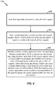
- the method 400 may be performed by the SIMD architecture 102 of FIG. 1 (e.g., the SIMD lanes 122-128) and/or the processor 301 of FIG. 3 using the first register 130 of FIGS. 1-3 , the second register 140 of FIGS. 1-3 , the output register 212 of FIG. 2 , the memory 302 of FIG. 3 , or any combination thereof.
- the SIMD architecture 102 of FIG. 1 e.g., the SIMD lanes 122-128
- the processor 301 of FIG. 3 using the first register 130 of FIGS. 1-3 , the second register 140 of FIGS. 1-3 , the output register 212 of FIG. 2 , the memory 302 of FIG. 3 , or any combination thereof.
- the method 400 includes storing first input data elements in a lane of a first register, at 402.
- the processor 301 may store the first input data elements 106 (e.g., data element "0" through data element "3") of the input data 104 into the first lane 132 of the first register 130.
- the processor 301 may load the first input data elements 106 into the first lane 132 of the first register 130 in response to receiving the load instruction.
- the processor 301 may store the second input data elements 108 (e.g., data element "4" through data element "7") of the input data 104 into the second lane 124 of the first register 130.
- the processor 301 may load the second input data elements 108 into the second lane 134 of the first register 130 in response to receiving the load instruction.
- Second input data elements may be stored in a lane of a second register, at 404.
- the processor 301 may store the second input data elements 108 of the input data into the first lane 142 of the second register 140.
- the processor 301 may retrieve the input data 104 from the memory location in the memory 302 and provide the input data 104 to the logic shifter circuit 304 upon receiving the load instruction.
- the logic shifter circuit 304 may shift the input data 104 by the lane width of the SIMD lanes 122-128.
- the logic shifter circuit 304 may shift the input data 104 by four to generate shifted input data 314.
- the processor may load the shifted input data 314 into the second register 140 according to the alignment depicted in FIG.
- data element "4" through data element "7" may be loaded into the first lane 142 of the second register 140.
- the width of the first lane 142 of the second register 140 may be equal to the width of the first lane 132 of the first register 130.
- a sliding window operation may be performed on the first input data elements in the lane of the first register and the second input data elements in the lane of the second register using a SIMD lane having a lane width equal to the width of the lane of the first register, at 406.
- a "sliding window operation" may include any operation in which multiple neighboring data elements (e.g., the first input data elements and the second input data elements) in a data stream are taken as data inputs and an output is produced.
- a sum of products is described above as a sliding window operation, it should be understood that a sum of products is merely one example.
- Other examples of sliding window operations may include a product of sums, summation operations, multiplication operations, etc.
- Performing the sliding window operation may include determining a result based on a first input data element stored in a first position of the first register and a second input data element stored in a second position of the second register that is different from the first position.
- the result of one sliding window operation may be based on data elements "1-4".
- Data element "1" may be in one position of the first register 130 (e.g., the second position) and data element "4" may be in another position of the second register 140 (e.g., the first position) that is different from the position of data element "1".
- the first SIMD lane 122 may perform up to five sliding window operations (e.g., five sliding window operations) using the first input data elements 106 stored in the first lane 132 of the first register 130 and using the second input data elements 108 stored in the first lane 142 of the second register 140.
- the number of sliding window operations (e.g., five) performed by the first SIMD lane 122 may be greater than or equal to the width (e.g., four) of the first SIMD lane 122.
- the method 400 of FIG. 4 may enable the first SIMD lane 122 to perform up to five sliding window operations using two registers 130, 140 and a single shift (e.g., a four data element shift between the registers 130, 140 by the logic shifter circuit 304 as depicted in FIG. 3 ) compared to another SIMD architecture that may require a single SIMD lane to use four registers and four shifts (e.g., four single-elements shifts). Because the data in the second register 140 is shifted by four instead of one, all of the data elements necessary to calculate up to five outputs are accessible to the first SIMD lane 122 using two registers 130, 140. Thus, a reduced number of registers and shifts may be utilized compared to other sliding window operations and SIMD architectures.
- the method 400 may include performing similar operations at additional SIMD lanes.
- the SIMD lanes 124-128 may operate in a substantially similar manner with respect to the corresponding lanes 134-138, 144-148 of the registers 130, 140, respectively, as the first SIMD lane 122 operates with respect to the first lanes 132, 142 of the registers 130, 140.
- the second SIMD lane 124 may perform up to five sliding window operations using the second input data elements 108 in the second lane 134 of the first register 130 and using the third input data elements in the second lane 144 of the second register 140.
- the third SIMD lane 126 may perform up to five sliding window operations using the third input data elements in the third lane 136 of the first register 130 and using the fourth input data elements in the third lane 146 of the second register 140. Additionally, the fourth SIMD lane 128 may perform up to five sliding window operations using the fourth input data elements in the fourth lane 138 of the first register 130 and using the fifth input data elements in the fourth lane 148 of the second register 140. Additional SIMD lanes (not shown) may operate in a substantially similar manner as the illustrated SIMD lanes 122-128 to perform sliding window operations on the remaining input data 104.
- the device 500 includes a processor 510, such as a digital signal processor, coupled to a memory 532.
- a processor 510 such as a digital signal processor
- the processor 510 is configured to execute software (e.g., a program of one or more instructions 568) stored in the memory 532.
- the processor 510 includes the SIMD architecture 102 of FIG. 1 , the first register 130 of FIG. 1 , and the second register 140 of FIG. 1 .
- the SIMD architecture 102 may be within an execution unit of the processor 510 and may reference the registers 130, 140 to perform convolution functions, as described above.
- the processor 510 may be operable to perform the method 400 of FIG. 4 .
- the processor 510 may store the first input data elements 106 in the first lane 132 of the first register 130 and may store the second input data elements 108 in the first lane 142 of the second register 140.
- the SIMD architecture 102 may perform up to five sliding window operations using the data elements stored in the first lanes 132, 142 of the registers 130, 140, respectively, as described above.
- the processor 510 may be configured to execute one or more instructions 568 stored in the memory 532 to perform the method 400 of FIG. 4 .
- the memory 532 may be a non-transitory computer-readable medium that includes instructions 568 that, when executed by the processor 510, cause the processor 510 to perform the method 400 of FIG. 4 .
- a wireless interface 540 may be coupled to the processor 510 and to an antenna 542.
- a coder/decoder (CODEC) 534 can also be coupled to the processor 510.
- a speaker 536 and a microphone 538 can be coupled to the CODEC 534.
- a display controller 526 can be coupled to the processor 510 and to a display device 528.
- the processor 510, the display controller 526, the memory 532, the CODEC 534, and the wireless interface 540 are included in a system-in-package or system-on-chip device 522.
- an input device 530 and a power supply 544 are coupled to the system-on-chip device 522.
- the display device 528, the input device 530, the speaker 536, the microphone 538, the antenna 542, and the power supply 544 are external to the system-on-chip device 522.
- each of the display device 528, the input device 530, the speaker 536, the microphone 538, the antenna 542, and the power supply 544 can be coupled to one or more components of the system-on-chip device 522, such as one or more interfaces or controllers.
- the convolution functions with respect to FIGS. 1-4 may be used to perform image processing at the device 500.
- the convolution functions may be applied to a kernel (e.g., a convolution matrix or a mask) to blur pixels of an image, to sharpen pixels of an image, to detect edges within an image, etc.
- a kernel e.g., a convolution matrix or a mask
- the device 500 may perform image processing using fewer registers and shifts compared to devices using other SIMD architectures.
- an apparatus includes first means for storing data.
- the first means for storing data has a lane storing first input data element.
- the first means for storing data may include the first register 130 of FIGS. 1-3 and 5 , one or more other devices, circuits, modules, or any combination thereof.
- the apparatus may also include second means for storing data.
- the second means for storing data has a lane storing second input data elements.
- the second means for storing data may include the second register 140 of FIGS. 1-3 and 5 , one or more other devices, circuits, modules, or any combination thereof.
- a width of the first lane of the second means for storing data is equal to a width of the first lane of the first means for storing data.
- the width (e.g., four) of the first lane 132 of the first register 130 may be equal to the width (e.g., four) of the first lane 142 of the second register 140.
- the apparatus may also include means for a performing sliding window operation on the first input data elements in the lane of the first means for storing data and the second input data elements in the lane of the second means for storing data.
- the means for performing the sliding window operations may include the SIMD architecture 102 of FIGS. 1 and 5 , the multiplexers 202-208 of FIG. 2 , the processor 301 of FIG. 3 , the instructions 568 executable by the processor 510 of FIG. 5 , one or more other devices, circuits, modules, or any combination thereof.
- the means for performing the sliding window operations has a lane width equal to the width of the lane of the first means for storing data.
- Performing the sliding window operation includes determining a result based on a first input data element stored in a first position of the first means for storing data and a second input data element stored in a second position of the second means for storing data.
- the second position is different from the first position.
- a software module may reside in random access memory (RAM), flash memory, read-only memory (ROM), programmable read-only memory (PROM), erasable programmable read-only memory (EPROM), electrically erasable programmable read-only memory (EEPROM), registers, hard disk, a removable disk, a compact disc read-only memory (CD-ROM), or any other form of storage medium known in the art.
- An exemplary non-transitory (e.g. tangible) storage medium is coupled to the processor such that the processor can read information from, and write information to, the storage medium.
- the storage medium may be integral to the processor.
- the processor and the storage medium may reside in an application-specific integrated circuit (ASIC).
- ASIC application-specific integrated circuit
- the ASIC may reside in a computing device or a user terminal.
- the processor and the storage medium may reside as discrete components in a computing device or user terminal.
Landscapes
- Engineering & Computer Science (AREA)
- Theoretical Computer Science (AREA)
- Software Systems (AREA)
- Physics & Mathematics (AREA)
- General Physics & Mathematics (AREA)
- General Engineering & Computer Science (AREA)
- Computer Hardware Design (AREA)
- Mathematical Physics (AREA)
- Computational Mathematics (AREA)
- Pure & Applied Mathematics (AREA)
- Mathematical Optimization (AREA)
- Mathematical Analysis (AREA)
- Executing Machine-Instructions (AREA)
- Complex Calculations (AREA)
- Advance Control (AREA)
Applications Claiming Priority (2)
| Application Number | Priority Date | Filing Date | Title |
|---|---|---|---|
| US14/803,728 US10459731B2 (en) | 2015-07-20 | 2015-07-20 | Sliding window operation |
| PCT/US2016/041779 WO2017014979A1 (en) | 2015-07-20 | 2016-07-11 | Simd sliding window operation |
Publications (2)
| Publication Number | Publication Date |
|---|---|
| EP3326061A1 EP3326061A1 (en) | 2018-05-30 |
| EP3326061B1 true EP3326061B1 (en) | 2022-05-25 |
Family
ID=56511938
Family Applications (1)
| Application Number | Title | Priority Date | Filing Date |
|---|---|---|---|
| EP16742134.6A Active EP3326061B1 (en) | 2015-07-20 | 2016-07-11 | Simd sliding window operation |
Country Status (8)
Families Citing this family (4)
| Publication number | Priority date | Publication date | Assignee | Title |
|---|---|---|---|---|
| US11803377B2 (en) * | 2017-09-08 | 2023-10-31 | Oracle International Corporation | Efficient direct convolution using SIMD instructions |
| US11403727B2 (en) | 2020-01-28 | 2022-08-02 | Nxp Usa, Inc. | System and method for convolving an image |
| CN113887695A (zh) * | 2020-07-03 | 2022-01-04 | 北京君正集成电路股份有限公司 | 一种基于simd的卷积运算的并行优化方法 |
| US11586442B2 (en) | 2020-08-06 | 2023-02-21 | Nxp Usa, Inc. | System and method for convolving image with sparse kernels |
Family Cites Families (20)
| Publication number | Priority date | Publication date | Assignee | Title |
|---|---|---|---|---|
| JPS5743239A (en) * | 1980-08-27 | 1982-03-11 | Hitachi Ltd | Data processor |
| US6009505A (en) * | 1996-12-02 | 1999-12-28 | Compaq Computer Corp. | System and method for routing one operand to arithmetic logic units from fixed register slots and another operand from any register slot |
| US6230253B1 (en) * | 1998-03-31 | 2001-05-08 | Intel Corporation | Executing partial-width packed data instructions |
| HK1048539A1 (zh) * | 2000-03-08 | 2003-04-04 | Sun Microsystems, Inc. | 设有次字元的置换功能及操作码(opcode)的修正功能的处理架构 |
| DE10023319B4 (de) * | 2000-05-12 | 2008-07-10 | Man Roland Druckmaschinen Ag | Verfahren zum Umspulen von Thermotransferband zum Bebildern von Druckformen |
| US7126991B1 (en) | 2003-02-03 | 2006-10-24 | Tibet MIMAR | Method for programmable motion estimation in a SIMD processor |
| US7275147B2 (en) * | 2003-03-31 | 2007-09-25 | Hitachi, Ltd. | Method and apparatus for data alignment and parsing in SIMD computer architecture |
| GB2409065B (en) | 2003-12-09 | 2006-10-25 | Advanced Risc Mach Ltd | Multiplexing operations in SIMD processing |
| US7933405B2 (en) | 2005-04-08 | 2011-04-26 | Icera Inc. | Data access and permute unit |
| US7761694B2 (en) * | 2006-06-30 | 2010-07-20 | Intel Corporation | Execution unit for performing shuffle and other operations |
| US20080100628A1 (en) | 2006-10-31 | 2008-05-01 | International Business Machines Corporation | Single Precision Vector Permute Immediate with "Word" Vector Write Mask |
| GB2444744B (en) * | 2006-12-12 | 2011-05-25 | Advanced Risc Mach Ltd | Apparatus and method for performing re-arrangement operations on data |
| WO2008077803A1 (en) | 2006-12-22 | 2008-07-03 | Telefonaktiebolaget L M Ericsson (Publ) | Simd processor with reduction unit |
| CN101021832A (zh) * | 2007-03-19 | 2007-08-22 | 中国人民解放军国防科学技术大学 | 支持局部寄存和条件执行的64位浮点整数融合运算群 |
| CN100461095C (zh) * | 2007-11-20 | 2009-02-11 | 浙江大学 | 一种支持多模式的媒体增强流水线乘法单元设计方法 |
| US9081501B2 (en) * | 2010-01-08 | 2015-07-14 | International Business Machines Corporation | Multi-petascale highly efficient parallel supercomputer |
| CN102012893B (zh) * | 2010-11-25 | 2012-07-18 | 中国人民解放军国防科学技术大学 | 一种可扩展向量运算装置 |
| US9588766B2 (en) * | 2012-09-28 | 2017-03-07 | Intel Corporation | Accelerated interlane vector reduction instructions |
| US9424031B2 (en) | 2013-03-13 | 2016-08-23 | Intel Corporation | Techniques for enabling bit-parallel wide string matching with a SIMD register |
| CN104699458A (zh) * | 2015-03-30 | 2015-06-10 | 哈尔滨工业大学 | 定点向量处理器及其向量数据访存控制方法 |
-
2015
- 2015-07-20 US US14/803,728 patent/US10459731B2/en active Active
-
2016
- 2016-07-11 CN CN201680039649.1A patent/CN107873091B/zh active Active
- 2016-07-11 JP JP2018502081A patent/JP6737869B2/ja active Active
- 2016-07-11 BR BR112018001183A patent/BR112018001183A2/pt not_active Application Discontinuation
- 2016-07-11 WO PCT/US2016/041779 patent/WO2017014979A1/en active Application Filing
- 2016-07-11 KR KR1020187001587A patent/KR102092049B1/ko active Active
- 2016-07-11 CA CA2990249A patent/CA2990249A1/en not_active Abandoned
- 2016-07-11 EP EP16742134.6A patent/EP3326061B1/en active Active
Also Published As
| Publication number | Publication date |
|---|---|
| EP3326061A1 (en) | 2018-05-30 |
| CN107873091B (zh) | 2021-05-28 |
| US10459731B2 (en) | 2019-10-29 |
| KR20180030540A (ko) | 2018-03-23 |
| JP6737869B2 (ja) | 2020-08-12 |
| BR112018001183A2 (pt) | 2018-09-11 |
| JP2018525730A (ja) | 2018-09-06 |
| WO2017014979A1 (en) | 2017-01-26 |
| CN107873091A (zh) | 2018-04-03 |
| CA2990249A1 (en) | 2017-01-26 |
| KR102092049B1 (ko) | 2020-04-20 |
| US20170024218A1 (en) | 2017-01-26 |
Similar Documents
| Publication | Publication Date | Title |
|---|---|---|
| US10474466B2 (en) | SIMD sign operation | |
| JP4750157B2 (ja) | データを右方向平行シフトマージする方法及び装置 | |
| EP3033670B1 (en) | Vector accumulation method and apparatus | |
| EP3326061B1 (en) | Simd sliding window operation | |
| TWI803634B (zh) | 子向量數值之加載及複製之處理器、操作一處理器之方法、處理設備及包含指令的非暫時性電腦可讀媒體 | |
| KR101697548B1 (ko) | Fifo 로드 명령 | |
| MXPA03011899A (es) | Un metodo, aparato, e instrucciones para efectuar una operacion de signo que multiplica. | |
| KR20050005730A (ko) | 라운드 및 시프트를 갖는 simd 정수 곱셈 하이 | |
| CN111506520B (zh) | 一种地址生成的方法、相关装置以及存储介质 | |
| EP4446878A1 (en) | Vector shifting method, processor, and electronic device | |
| EP3335127A1 (en) | Simd multiply and horizontal reduce operations | |
| KR102121866B1 (ko) | 와이드 데이터 엘리먼트들에 대한 레지스터 쌍을 사용하는 짝수-엘리먼트 및 홀수-엘리먼트 연산들을 가지는 혼합-폭 simd 연산들 | |
| CN114746840A (zh) | 用于乘法和累加操作的处理器单元 | |
| CN108139886B (zh) | 用于图像处理器的多功能执行通道 | |
| CN105630467B (zh) | 用户交互界面的渲染处理方法及处理装置 | |
| WO2022191859A1 (en) | Vector processing using vector-specific data type | |
| US12271732B1 (en) | Configuration of a deep vector engine using an opcode table, control table, and datapath table | |
| US20150006850A1 (en) | Processor with heterogeneous clustered architecture |
Legal Events
| Date | Code | Title | Description |
|---|---|---|---|
| STAA | Information on the status of an ep patent application or granted ep patent |
Free format text: STATUS: THE INTERNATIONAL PUBLICATION HAS BEEN MADE |
|
| PUAI | Public reference made under article 153(3) epc to a published international application that has entered the european phase |
Free format text: ORIGINAL CODE: 0009012 |
|
| STAA | Information on the status of an ep patent application or granted ep patent |
Free format text: STATUS: REQUEST FOR EXAMINATION WAS MADE |
|
| 17P | Request for examination filed |
Effective date: 20171213 |
|
| AK | Designated contracting states |
Kind code of ref document: A1 Designated state(s): AL AT BE BG CH CY CZ DE DK EE ES FI FR GB GR HR HU IE IS IT LI LT LU LV MC MK MT NL NO PL PT RO RS SE SI SK SM TR |
|
| AX | Request for extension of the european patent |
Extension state: BA ME |
|
| DAV | Request for validation of the european patent (deleted) | ||
| DAX | Request for extension of the european patent (deleted) | ||
| GRAP | Despatch of communication of intention to grant a patent |
Free format text: ORIGINAL CODE: EPIDOSNIGR1 |
|
| STAA | Information on the status of an ep patent application or granted ep patent |
Free format text: STATUS: GRANT OF PATENT IS INTENDED |
|
| INTG | Intention to grant announced |
Effective date: 20210712 |
|
| GRAJ | Information related to disapproval of communication of intention to grant by the applicant or resumption of examination proceedings by the epo deleted |
Free format text: ORIGINAL CODE: EPIDOSDIGR1 |
|
| STAA | Information on the status of an ep patent application or granted ep patent |
Free format text: STATUS: REQUEST FOR EXAMINATION WAS MADE |
|
| INTC | Intention to grant announced (deleted) | ||
| GRAP | Despatch of communication of intention to grant a patent |
Free format text: ORIGINAL CODE: EPIDOSNIGR1 |
|
| STAA | Information on the status of an ep patent application or granted ep patent |
Free format text: STATUS: GRANT OF PATENT IS INTENDED |
|
| INTG | Intention to grant announced |
Effective date: 20211221 |
|
| GRAS | Grant fee paid |
Free format text: ORIGINAL CODE: EPIDOSNIGR3 |
|
| GRAA | (expected) grant |
Free format text: ORIGINAL CODE: 0009210 |
|
| STAA | Information on the status of an ep patent application or granted ep patent |
Free format text: STATUS: THE PATENT HAS BEEN GRANTED |
|
| AK | Designated contracting states |
Kind code of ref document: B1 Designated state(s): AL AT BE BG CH CY CZ DE DK EE ES FI FR GB GR HR HU IE IS IT LI LT LU LV MC MK MT NL NO PL PT RO RS SE SI SK SM TR |
|
| REG | Reference to a national code |
Ref country code: GB Ref legal event code: FG4D |
|
| REG | Reference to a national code |
Ref country code: CH Ref legal event code: EP |
|
| REG | Reference to a national code |
Ref country code: AT Ref legal event code: REF Ref document number: 1494531 Country of ref document: AT Kind code of ref document: T Effective date: 20220615 Ref country code: DE Ref legal event code: R096 Ref document number: 602016072381 Country of ref document: DE |
|
| REG | Reference to a national code |
Ref country code: IE Ref legal event code: FG4D |
|
| REG | Reference to a national code |
Ref country code: LT Ref legal event code: MG9D |
|
| REG | Reference to a national code |
Ref country code: NL Ref legal event code: MP Effective date: 20220525 |
|
| REG | Reference to a national code |
Ref country code: AT Ref legal event code: MK05 Ref document number: 1494531 Country of ref document: AT Kind code of ref document: T Effective date: 20220525 |
|
| PG25 | Lapsed in a contracting state [announced via postgrant information from national office to epo] |
Ref country code: SE Free format text: LAPSE BECAUSE OF FAILURE TO SUBMIT A TRANSLATION OF THE DESCRIPTION OR TO PAY THE FEE WITHIN THE PRESCRIBED TIME-LIMIT Effective date: 20220525 Ref country code: PT Free format text: LAPSE BECAUSE OF FAILURE TO SUBMIT A TRANSLATION OF THE DESCRIPTION OR TO PAY THE FEE WITHIN THE PRESCRIBED TIME-LIMIT Effective date: 20220926 Ref country code: NO Free format text: LAPSE BECAUSE OF FAILURE TO SUBMIT A TRANSLATION OF THE DESCRIPTION OR TO PAY THE FEE WITHIN THE PRESCRIBED TIME-LIMIT Effective date: 20220825 Ref country code: NL Free format text: LAPSE BECAUSE OF FAILURE TO SUBMIT A TRANSLATION OF THE DESCRIPTION OR TO PAY THE FEE WITHIN THE PRESCRIBED TIME-LIMIT Effective date: 20220525 Ref country code: LT Free format text: LAPSE BECAUSE OF FAILURE TO SUBMIT A TRANSLATION OF THE DESCRIPTION OR TO PAY THE FEE WITHIN THE PRESCRIBED TIME-LIMIT Effective date: 20220525 Ref country code: HR Free format text: LAPSE BECAUSE OF FAILURE TO SUBMIT A TRANSLATION OF THE DESCRIPTION OR TO PAY THE FEE WITHIN THE PRESCRIBED TIME-LIMIT Effective date: 20220525 Ref country code: GR Free format text: LAPSE BECAUSE OF FAILURE TO SUBMIT A TRANSLATION OF THE DESCRIPTION OR TO PAY THE FEE WITHIN THE PRESCRIBED TIME-LIMIT Effective date: 20220826 Ref country code: FI Free format text: LAPSE BECAUSE OF FAILURE TO SUBMIT A TRANSLATION OF THE DESCRIPTION OR TO PAY THE FEE WITHIN THE PRESCRIBED TIME-LIMIT Effective date: 20220525 Ref country code: ES Free format text: LAPSE BECAUSE OF FAILURE TO SUBMIT A TRANSLATION OF THE DESCRIPTION OR TO PAY THE FEE WITHIN THE PRESCRIBED TIME-LIMIT Effective date: 20220525 Ref country code: BG Free format text: LAPSE BECAUSE OF FAILURE TO SUBMIT A TRANSLATION OF THE DESCRIPTION OR TO PAY THE FEE WITHIN THE PRESCRIBED TIME-LIMIT Effective date: 20220825 Ref country code: AT Free format text: LAPSE BECAUSE OF FAILURE TO SUBMIT A TRANSLATION OF THE DESCRIPTION OR TO PAY THE FEE WITHIN THE PRESCRIBED TIME-LIMIT Effective date: 20220525 |
|
| PG25 | Lapsed in a contracting state [announced via postgrant information from national office to epo] |
Ref country code: RS Free format text: LAPSE BECAUSE OF FAILURE TO SUBMIT A TRANSLATION OF THE DESCRIPTION OR TO PAY THE FEE WITHIN THE PRESCRIBED TIME-LIMIT Effective date: 20220525 Ref country code: PL Free format text: LAPSE BECAUSE OF FAILURE TO SUBMIT A TRANSLATION OF THE DESCRIPTION OR TO PAY THE FEE WITHIN THE PRESCRIBED TIME-LIMIT Effective date: 20220525 Ref country code: LV Free format text: LAPSE BECAUSE OF FAILURE TO SUBMIT A TRANSLATION OF THE DESCRIPTION OR TO PAY THE FEE WITHIN THE PRESCRIBED TIME-LIMIT Effective date: 20220525 Ref country code: IS Free format text: LAPSE BECAUSE OF FAILURE TO SUBMIT A TRANSLATION OF THE DESCRIPTION OR TO PAY THE FEE WITHIN THE PRESCRIBED TIME-LIMIT Effective date: 20220925 |
|
| PG25 | Lapsed in a contracting state [announced via postgrant information from national office to epo] |
Ref country code: SM Free format text: LAPSE BECAUSE OF FAILURE TO SUBMIT A TRANSLATION OF THE DESCRIPTION OR TO PAY THE FEE WITHIN THE PRESCRIBED TIME-LIMIT Effective date: 20220525 Ref country code: SK Free format text: LAPSE BECAUSE OF FAILURE TO SUBMIT A TRANSLATION OF THE DESCRIPTION OR TO PAY THE FEE WITHIN THE PRESCRIBED TIME-LIMIT Effective date: 20220525 Ref country code: RO Free format text: LAPSE BECAUSE OF FAILURE TO SUBMIT A TRANSLATION OF THE DESCRIPTION OR TO PAY THE FEE WITHIN THE PRESCRIBED TIME-LIMIT Effective date: 20220525 Ref country code: EE Free format text: LAPSE BECAUSE OF FAILURE TO SUBMIT A TRANSLATION OF THE DESCRIPTION OR TO PAY THE FEE WITHIN THE PRESCRIBED TIME-LIMIT Effective date: 20220525 Ref country code: DK Free format text: LAPSE BECAUSE OF FAILURE TO SUBMIT A TRANSLATION OF THE DESCRIPTION OR TO PAY THE FEE WITHIN THE PRESCRIBED TIME-LIMIT Effective date: 20220525 Ref country code: CZ Free format text: LAPSE BECAUSE OF FAILURE TO SUBMIT A TRANSLATION OF THE DESCRIPTION OR TO PAY THE FEE WITHIN THE PRESCRIBED TIME-LIMIT Effective date: 20220525 |
|
| PG25 | Lapsed in a contracting state [announced via postgrant information from national office to epo] |
Ref country code: MC Free format text: LAPSE BECAUSE OF FAILURE TO SUBMIT A TRANSLATION OF THE DESCRIPTION OR TO PAY THE FEE WITHIN THE PRESCRIBED TIME-LIMIT Effective date: 20220525 |
|
| REG | Reference to a national code |
Ref country code: DE Ref legal event code: R097 Ref document number: 602016072381 Country of ref document: DE Ref country code: CH Ref legal event code: PL |
|
| REG | Reference to a national code |
Ref country code: BE Ref legal event code: MM Effective date: 20220731 |
|
| PG25 | Lapsed in a contracting state [announced via postgrant information from national office to epo] |
Ref country code: AL Free format text: LAPSE BECAUSE OF FAILURE TO SUBMIT A TRANSLATION OF THE DESCRIPTION OR TO PAY THE FEE WITHIN THE PRESCRIBED TIME-LIMIT Effective date: 20220525 |
|
| PLBE | No opposition filed within time limit |
Free format text: ORIGINAL CODE: 0009261 |
|
| STAA | Information on the status of an ep patent application or granted ep patent |
Free format text: STATUS: NO OPPOSITION FILED WITHIN TIME LIMIT |
|
| PG25 | Lapsed in a contracting state [announced via postgrant information from national office to epo] |
Ref country code: LU Free format text: LAPSE BECAUSE OF NON-PAYMENT OF DUE FEES Effective date: 20220711 Ref country code: LI Free format text: LAPSE BECAUSE OF NON-PAYMENT OF DUE FEES Effective date: 20220731 Ref country code: CH Free format text: LAPSE BECAUSE OF NON-PAYMENT OF DUE FEES Effective date: 20220731 |
|
| 26N | No opposition filed |
Effective date: 20230228 |
|
| PG25 | Lapsed in a contracting state [announced via postgrant information from national office to epo] |
Ref country code: SI Free format text: LAPSE BECAUSE OF FAILURE TO SUBMIT A TRANSLATION OF THE DESCRIPTION OR TO PAY THE FEE WITHIN THE PRESCRIBED TIME-LIMIT Effective date: 20220525 Ref country code: BE Free format text: LAPSE BECAUSE OF NON-PAYMENT OF DUE FEES Effective date: 20220731 |
|
| PG25 | Lapsed in a contracting state [announced via postgrant information from national office to epo] |
Ref country code: IE Free format text: LAPSE BECAUSE OF NON-PAYMENT OF DUE FEES Effective date: 20220711 |
|
| PG25 | Lapsed in a contracting state [announced via postgrant information from national office to epo] |
Ref country code: IT Free format text: LAPSE BECAUSE OF FAILURE TO SUBMIT A TRANSLATION OF THE DESCRIPTION OR TO PAY THE FEE WITHIN THE PRESCRIBED TIME-LIMIT Effective date: 20220525 |
|
| PG25 | Lapsed in a contracting state [announced via postgrant information from national office to epo] |
Ref country code: HU Free format text: LAPSE BECAUSE OF FAILURE TO SUBMIT A TRANSLATION OF THE DESCRIPTION OR TO PAY THE FEE WITHIN THE PRESCRIBED TIME-LIMIT; INVALID AB INITIO Effective date: 20160711 |
|
| PG25 | Lapsed in a contracting state [announced via postgrant information from national office to epo] |
Ref country code: MK Free format text: LAPSE BECAUSE OF FAILURE TO SUBMIT A TRANSLATION OF THE DESCRIPTION OR TO PAY THE FEE WITHIN THE PRESCRIBED TIME-LIMIT Effective date: 20220525 Ref country code: CY Free format text: LAPSE BECAUSE OF FAILURE TO SUBMIT A TRANSLATION OF THE DESCRIPTION OR TO PAY THE FEE WITHIN THE PRESCRIBED TIME-LIMIT Effective date: 20220525 |
|
| PG25 | Lapsed in a contracting state [announced via postgrant information from national office to epo] |
Ref country code: TR Free format text: LAPSE BECAUSE OF FAILURE TO SUBMIT A TRANSLATION OF THE DESCRIPTION OR TO PAY THE FEE WITHIN THE PRESCRIBED TIME-LIMIT Effective date: 20220525 |
|
| PG25 | Lapsed in a contracting state [announced via postgrant information from national office to epo] |
Ref country code: MT Free format text: LAPSE BECAUSE OF FAILURE TO SUBMIT A TRANSLATION OF THE DESCRIPTION OR TO PAY THE FEE WITHIN THE PRESCRIBED TIME-LIMIT Effective date: 20220525 |
|
| PGFP | Annual fee paid to national office [announced via postgrant information from national office to epo] |
Ref country code: DE Payment date: 20240613 Year of fee payment: 9 |
|
| PG25 | Lapsed in a contracting state [announced via postgrant information from national office to epo] |
Ref country code: BG Free format text: LAPSE BECAUSE OF FAILURE TO SUBMIT A TRANSLATION OF THE DESCRIPTION OR TO PAY THE FEE WITHIN THE PRESCRIBED TIME-LIMIT Effective date: 20220525 |
|
| PG25 | Lapsed in a contracting state [announced via postgrant information from national office to epo] |
Ref country code: BG Free format text: LAPSE BECAUSE OF FAILURE TO SUBMIT A TRANSLATION OF THE DESCRIPTION OR TO PAY THE FEE WITHIN THE PRESCRIBED TIME-LIMIT Effective date: 20220525 |
|
| PGFP | Annual fee paid to national office [announced via postgrant information from national office to epo] |
Ref country code: GB Payment date: 20250612 Year of fee payment: 10 |
|
| PGFP | Annual fee paid to national office [announced via postgrant information from national office to epo] |
Ref country code: FR Payment date: 20250612 Year of fee payment: 10 |