EP3324456A1 - Ultra-fast method for preparing organic/organic thin film by using self-diffusion effects - Google Patents
Ultra-fast method for preparing organic/organic thin film by using self-diffusion effects Download PDFInfo
- Publication number
- EP3324456A1 EP3324456A1 EP16824591.8A EP16824591A EP3324456A1 EP 3324456 A1 EP3324456 A1 EP 3324456A1 EP 16824591 A EP16824591 A EP 16824591A EP 3324456 A1 EP3324456 A1 EP 3324456A1
- Authority
- EP
- European Patent Office
- Prior art keywords
- organic
- thin film
- inorganic
- substrate
- derivative
- Prior art date
- Legal status (The legal status is an assumption and is not a legal conclusion. Google has not performed a legal analysis and makes no representation as to the accuracy of the status listed.)
- Withdrawn
Links
Images




Classifications
-
- H—ELECTRICITY
- H10—SEMICONDUCTOR DEVICES; ELECTRIC SOLID-STATE DEVICES NOT OTHERWISE PROVIDED FOR
- H10K—ORGANIC ELECTRIC SOLID-STATE DEVICES
- H10K71/00—Manufacture or treatment specially adapted for the organic devices covered by this subclass
- H10K71/10—Deposition of organic active material
- H10K71/12—Deposition of organic active material using liquid deposition, e.g. spin coating
-
- H—ELECTRICITY
- H10—SEMICONDUCTOR DEVICES; ELECTRIC SOLID-STATE DEVICES NOT OTHERWISE PROVIDED FOR
- H10K—ORGANIC ELECTRIC SOLID-STATE DEVICES
- H10K10/00—Organic devices specially adapted for rectifying, amplifying, oscillating or switching; Organic capacitors or resistors having potential barriers
- H10K10/40—Organic transistors
- H10K10/46—Field-effect transistors, e.g. organic thin-film transistors [OTFT]
- H10K10/462—Insulated gate field-effect transistors [IGFETs]
- H10K10/466—Lateral bottom-gate IGFETs comprising only a single gate
-
- H—ELECTRICITY
- H10—SEMICONDUCTOR DEVICES; ELECTRIC SOLID-STATE DEVICES NOT OTHERWISE PROVIDED FOR
- H10K—ORGANIC ELECTRIC SOLID-STATE DEVICES
- H10K10/00—Organic devices specially adapted for rectifying, amplifying, oscillating or switching; Organic capacitors or resistors having potential barriers
- H10K10/40—Organic transistors
- H10K10/46—Field-effect transistors, e.g. organic thin-film transistors [OTFT]
- H10K10/462—Insulated gate field-effect transistors [IGFETs]
- H10K10/484—Insulated gate field-effect transistors [IGFETs] characterised by the channel regions
-
- H—ELECTRICITY
- H10—SEMICONDUCTOR DEVICES; ELECTRIC SOLID-STATE DEVICES NOT OTHERWISE PROVIDED FOR
- H10K—ORGANIC ELECTRIC SOLID-STATE DEVICES
- H10K30/00—Organic devices sensitive to infrared radiation, light, electromagnetic radiation of shorter wavelength or corpuscular radiation
- H10K30/10—Organic devices sensitive to infrared radiation, light, electromagnetic radiation of shorter wavelength or corpuscular radiation comprising heterojunctions between organic semiconductors and inorganic semiconductors
-
- H—ELECTRICITY
- H10—SEMICONDUCTOR DEVICES; ELECTRIC SOLID-STATE DEVICES NOT OTHERWISE PROVIDED FOR
- H10K—ORGANIC ELECTRIC SOLID-STATE DEVICES
- H10K50/00—Organic light-emitting devices
- H10K50/10—OLEDs or polymer light-emitting diodes [PLED]
- H10K50/11—OLEDs or polymer light-emitting diodes [PLED] characterised by the electroluminescent [EL] layers
-
- H—ELECTRICITY
- H10—SEMICONDUCTOR DEVICES; ELECTRIC SOLID-STATE DEVICES NOT OTHERWISE PROVIDED FOR
- H10K—ORGANIC ELECTRIC SOLID-STATE DEVICES
- H10K71/00—Manufacture or treatment specially adapted for the organic devices covered by this subclass
-
- H—ELECTRICITY
- H10—SEMICONDUCTOR DEVICES; ELECTRIC SOLID-STATE DEVICES NOT OTHERWISE PROVIDED FOR
- H10K—ORGANIC ELECTRIC SOLID-STATE DEVICES
- H10K71/00—Manufacture or treatment specially adapted for the organic devices covered by this subclass
- H10K71/80—Manufacture or treatment specially adapted for the organic devices covered by this subclass using temporary substrates
-
- H—ELECTRICITY
- H10—SEMICONDUCTOR DEVICES; ELECTRIC SOLID-STATE DEVICES NOT OTHERWISE PROVIDED FOR
- H10K—ORGANIC ELECTRIC SOLID-STATE DEVICES
- H10K77/00—Constructional details of devices covered by this subclass and not covered by groups H10K10/80, H10K30/80, H10K50/80 or H10K59/80
- H10K77/10—Substrates, e.g. flexible substrates
-
- H—ELECTRICITY
- H10—SEMICONDUCTOR DEVICES; ELECTRIC SOLID-STATE DEVICES NOT OTHERWISE PROVIDED FOR
- H10K—ORGANIC ELECTRIC SOLID-STATE DEVICES
- H10K77/00—Constructional details of devices covered by this subclass and not covered by groups H10K10/80, H10K30/80, H10K50/80 or H10K59/80
- H10K77/10—Substrates, e.g. flexible substrates
- H10K77/111—Flexible substrates
-
- H—ELECTRICITY
- H10—SEMICONDUCTOR DEVICES; ELECTRIC SOLID-STATE DEVICES NOT OTHERWISE PROVIDED FOR
- H10K—ORGANIC ELECTRIC SOLID-STATE DEVICES
- H10K85/00—Organic materials used in the body or electrodes of devices covered by this subclass
- H10K85/50—Organic perovskites; Hybrid organic-inorganic perovskites [HOIP], e.g. CH3NH3PbI3
-
- H—ELECTRICITY
- H10—SEMICONDUCTOR DEVICES; ELECTRIC SOLID-STATE DEVICES NOT OTHERWISE PROVIDED FOR
- H10K—ORGANIC ELECTRIC SOLID-STATE DEVICES
- H10K85/00—Organic materials used in the body or electrodes of devices covered by this subclass
- H10K85/701—Langmuir Blodgett films
-
- B—PERFORMING OPERATIONS; TRANSPORTING
- B05—SPRAYING OR ATOMISING IN GENERAL; APPLYING FLUENT MATERIALS TO SURFACES, IN GENERAL
- B05D—PROCESSES FOR APPLYING FLUENT MATERIALS TO SURFACES, IN GENERAL
- B05D1/00—Processes for applying liquids or other fluent materials
- B05D1/18—Processes for applying liquids or other fluent materials performed by dipping
- B05D1/20—Processes for applying liquids or other fluent materials performed by dipping substances to be applied floating on a fluid
- B05D1/202—Langmuir Blodgett films (LB films)
- B05D1/204—LB techniques
-
- H—ELECTRICITY
- H10—SEMICONDUCTOR DEVICES; ELECTRIC SOLID-STATE DEVICES NOT OTHERWISE PROVIDED FOR
- H10K—ORGANIC ELECTRIC SOLID-STATE DEVICES
- H10K2102/00—Constructional details relating to the organic devices covered by this subclass
- H10K2102/301—Details of OLEDs
- H10K2102/311—Flexible OLED
-
- H—ELECTRICITY
- H10—SEMICONDUCTOR DEVICES; ELECTRIC SOLID-STATE DEVICES NOT OTHERWISE PROVIDED FOR
- H10K—ORGANIC ELECTRIC SOLID-STATE DEVICES
- H10K30/00—Organic devices sensitive to infrared radiation, light, electromagnetic radiation of shorter wavelength or corpuscular radiation
- H10K30/30—Organic devices sensitive to infrared radiation, light, electromagnetic radiation of shorter wavelength or corpuscular radiation comprising bulk heterojunctions, e.g. interpenetrating networks of donor and acceptor material domains
-
- H—ELECTRICITY
- H10—SEMICONDUCTOR DEVICES; ELECTRIC SOLID-STATE DEVICES NOT OTHERWISE PROVIDED FOR
- H10K—ORGANIC ELECTRIC SOLID-STATE DEVICES
- H10K30/00—Organic devices sensitive to infrared radiation, light, electromagnetic radiation of shorter wavelength or corpuscular radiation
- H10K30/50—Photovoltaic [PV] devices
-
- H—ELECTRICITY
- H10—SEMICONDUCTOR DEVICES; ELECTRIC SOLID-STATE DEVICES NOT OTHERWISE PROVIDED FOR
- H10K—ORGANIC ELECTRIC SOLID-STATE DEVICES
- H10K50/00—Organic light-emitting devices
- H10K50/10—OLEDs or polymer light-emitting diodes [PLED]
- H10K50/11—OLEDs or polymer light-emitting diodes [PLED] characterised by the electroluminescent [EL] layers
- H10K50/12—OLEDs or polymer light-emitting diodes [PLED] characterised by the electroluminescent [EL] layers comprising dopants
-
- H—ELECTRICITY
- H10—SEMICONDUCTOR DEVICES; ELECTRIC SOLID-STATE DEVICES NOT OTHERWISE PROVIDED FOR
- H10K—ORGANIC ELECTRIC SOLID-STATE DEVICES
- H10K50/00—Organic light-emitting devices
- H10K50/10—OLEDs or polymer light-emitting diodes [PLED]
- H10K50/14—Carrier transporting layers
- H10K50/15—Hole transporting layers
-
- H—ELECTRICITY
- H10—SEMICONDUCTOR DEVICES; ELECTRIC SOLID-STATE DEVICES NOT OTHERWISE PROVIDED FOR
- H10K—ORGANIC ELECTRIC SOLID-STATE DEVICES
- H10K85/00—Organic materials used in the body or electrodes of devices covered by this subclass
- H10K85/10—Organic polymers or oligomers
- H10K85/111—Organic polymers or oligomers comprising aromatic, heteroaromatic, or aryl chains, e.g. polyaniline, polyphenylene or polyphenylene vinylene
-
- H—ELECTRICITY
- H10—SEMICONDUCTOR DEVICES; ELECTRIC SOLID-STATE DEVICES NOT OTHERWISE PROVIDED FOR
- H10K—ORGANIC ELECTRIC SOLID-STATE DEVICES
- H10K85/00—Organic materials used in the body or electrodes of devices covered by this subclass
- H10K85/10—Organic polymers or oligomers
- H10K85/111—Organic polymers or oligomers comprising aromatic, heteroaromatic, or aryl chains, e.g. polyaniline, polyphenylene or polyphenylene vinylene
- H10K85/113—Heteroaromatic compounds comprising sulfur or selene, e.g. polythiophene
-
- H—ELECTRICITY
- H10—SEMICONDUCTOR DEVICES; ELECTRIC SOLID-STATE DEVICES NOT OTHERWISE PROVIDED FOR
- H10K—ORGANIC ELECTRIC SOLID-STATE DEVICES
- H10K85/00—Organic materials used in the body or electrodes of devices covered by this subclass
- H10K85/10—Organic polymers or oligomers
- H10K85/151—Copolymers
-
- H—ELECTRICITY
- H10—SEMICONDUCTOR DEVICES; ELECTRIC SOLID-STATE DEVICES NOT OTHERWISE PROVIDED FOR
- H10K—ORGANIC ELECTRIC SOLID-STATE DEVICES
- H10K85/00—Organic materials used in the body or electrodes of devices covered by this subclass
- H10K85/20—Carbon compounds, e.g. carbon nanotubes or fullerenes
- H10K85/211—Fullerenes, e.g. C60
- H10K85/215—Fullerenes, e.g. C60 comprising substituents, e.g. PCBM
-
- H—ELECTRICITY
- H10—SEMICONDUCTOR DEVICES; ELECTRIC SOLID-STATE DEVICES NOT OTHERWISE PROVIDED FOR
- H10K—ORGANIC ELECTRIC SOLID-STATE DEVICES
- H10K85/00—Organic materials used in the body or electrodes of devices covered by this subclass
- H10K85/30—Coordination compounds
-
- Y—GENERAL TAGGING OF NEW TECHNOLOGICAL DEVELOPMENTS; GENERAL TAGGING OF CROSS-SECTIONAL TECHNOLOGIES SPANNING OVER SEVERAL SECTIONS OF THE IPC; TECHNICAL SUBJECTS COVERED BY FORMER USPC CROSS-REFERENCE ART COLLECTIONS [XRACs] AND DIGESTS
- Y02—TECHNOLOGIES OR APPLICATIONS FOR MITIGATION OR ADAPTATION AGAINST CLIMATE CHANGE
- Y02E—REDUCTION OF GREENHOUSE GAS [GHG] EMISSIONS, RELATED TO ENERGY GENERATION, TRANSMISSION OR DISTRIBUTION
- Y02E10/00—Energy generation through renewable energy sources
- Y02E10/50—Photovoltaic [PV] energy
- Y02E10/549—Organic PV cells
-
- Y—GENERAL TAGGING OF NEW TECHNOLOGICAL DEVELOPMENTS; GENERAL TAGGING OF CROSS-SECTIONAL TECHNOLOGIES SPANNING OVER SEVERAL SECTIONS OF THE IPC; TECHNICAL SUBJECTS COVERED BY FORMER USPC CROSS-REFERENCE ART COLLECTIONS [XRACs] AND DIGESTS
- Y02—TECHNOLOGIES OR APPLICATIONS FOR MITIGATION OR ADAPTATION AGAINST CLIMATE CHANGE
- Y02P—CLIMATE CHANGE MITIGATION TECHNOLOGIES IN THE PRODUCTION OR PROCESSING OF GOODS
- Y02P70/00—Climate change mitigation technologies in the production process for final industrial or consumer products
- Y02P70/50—Manufacturing or production processes characterised by the final manufactured product
Definitions
- the present disclosure provides a method for forming a thin film on a liquid substrate. Specifically, it relates to a method for forming an organic/inorganic thin film through the surface tension between a liquid substrate and a solution by supplying the solution to the liquid substrate.
- organic/inorganic thin film is a fundamental technology in nanotechnology. It is a technology essential for most electronic devices such as mobile phones, military equipment, solar cells, etc., which need to be lightweight, thin and bendable.
- Vacuum deposition has been the representative technology for formation of an organic/inorganic thin film since the mid-20th century. There has been a lot of advancement focused on electronic materials and many methods have been proposed.
- the vacuum deposition techniques include physical deposition and chemical deposition methods.
- the wet deposition techniques include electro-plating, spin coating, slot-die coating, etc.
- Organic solar cells can be given as an example of the reason why a new technology for forming organic thin films is necessary.
- the organic solar is drawing attentions as a next-generation solar cell because it can be produced at low cost and is light and flexible. With low price and light weight, it is applicable to most fields where energy harvesting is necessary, such as batteries for mobile phones, military equipment, etc.
- the spin coating method has been considered the most effective method for fabricating high-efficiency organic solar cells capable of controlling nanomorphology, it is disadvantageous in that it is inappropriate for commercialization because it is impossible to achieve large-area thin film.
- large-area thin film can be achieved with many thin film forming methods such as doctor blading, slot-die coating, etc., it is difficult to fabricate high-efficiency organic solar cells due to the difficulty in forming uniform thin films because they are very sensitive to such factors as ink composition, interaction between the ink and the surface, etc.
- Patent document 1 KR 10-1189172 B .
- the present disclosure is directed to providing a method for forming a uniform single-layer or multi-layer organic/inorganic thin film with improved air-stability very quickly and effectively on a liquid substrate with little material loss by using the difference in surface tension between solutions.
- An ultra-fast method for forming an organic/inorganic thin film by using a spontaneous spreading effect includes: a step of preparing a solution by dissolving one or more organic/inorganic material in a solvent; a step of forming an organic/inorganic thin film by supplying the prepared solution onto a liquid substrate; and a step of transferring the formed thin film to a substrate, wherein, in the step of forming the organic/inorganic thin film, the organic/inorganic material forms the thin film on the liquid substrate through a spontaneous spreading phenomenon caused by a difference in surface tension between the liquid substrate and the solution and through evaporation of the solvent and a dissolution process of the solvent to the liquid substrate.
- a single-layer or multi-layer thin film is formed on the liquid substrate by a solution wherein a single or composite organic/inorganic material is dissolved in a solvent.
- the organic/inorganic material includes one or more of an organic compound including a conjugated polymer or a conjugated small molecule such as a polybenzothiophene derivative, a polythiophene derivative, a poly(p-phenylene) derivative, a polyfluorene derivative, a polyacetylene derivative, a polypyrrole derivative, a polyvinylcarbazole derivative, a polyaniline derivative and a polyphenylenevinylene derivative, an n-type polymer compound such as a polyperylene derivative, a fullerene derivative such as fullerene (C 60 ), [6,6]-phenyl-C 61 -butyric acid methyl ether (PCBM), [6,6]-phenyl-C 71 -butyric acid methyl ether (PC70BM), an inorganic/organic hybrid perovskite compound of a perovskite structure containing an amidinium ion and an organic ammonium ion as monovalent organic
- the liquid substrate is one having a higher surface tension than the solvent, selected from a group consisting of distilled water, glycerol, formamide and ethylene glycol.
- the solvent is one capable of dissolving the organic/inorganic material and having a difference in surface tension with the liquid substrate such that a spontaneous spreading effect can occur, selected from a group consisting of chlorobenzene, chloroform, toluene and dichlorobenzene.
- the substrate to which the organic/inorganic thin film is transferred is one of a flexible polymer substrate, a metal substrate and a glass substrate.
- the flexible polymer substrate is one selected from a group consisting of polydimethylsiloxane (PDMS), polyethylene terephthalate (PET), polyethylene naphthalate (PEN) polyethylene (PE), polyethersulfone (PES), polycarbonate (PC), polyarylate (PAR) and polyimide (PI).
- PDMS polydimethylsiloxane
- PET polyethylene terephthalate
- PEN polyethylene naphthalate
- PE polyethylene
- PES polyethersulfone
- PC polycarbonate
- PAR polyarylate
- PI polyimide
- the metal substrate is one selected from a group consisting of SUS (steel use stainless), aluminum, steel and copper.
- the present disclosure provides an organic/inorganic thin film prepared by the method for forming an organic/inorganic thin film described above.
- the present disclosure provides an organic/inorganic electronic device containing the organic/inorganic thin film.
- the organic/inorganic electronic device is one of a solar cell, a light-emitting diode and a transistor.
- the present disclosure relates to a method for forming an organic/inorganic thin film on a liquid substrate by using the surface tension between the liquid substrate and a solution and allows for fabrication of an organic/inorganic electronic device including a solar cell, a light-emitting diode, a thin-film transistor, etc.
- a uniform organic/inorganic thin film can be formed very quickly and effectively with little material loss and the process is very simple because the formed thin film can be transferred freely to a glass, plastic or metal substrate without additional treatment.
- the present disclosure can improve the efficiency of an organic/inorganic electronic device because the nanomorphology of the thin film can be controlled effectively during the crystallization, orientation and phase separation of materials.
- the organic/inorganic solution used for spin coating can be utilized without modification. That is to say, the present disclosure solves the problems occurring during thin film formation by the conventional spin coating method that about 90% or more material is lost and it is difficult to attain a uniform thin film because a lot of time is required for optimization due to high sensitivity to such factors as ink composition, interaction between the ink and the surface, etc.
- the present disclosure allows for effective formation of a multi-layer thin film without limitation to solvent or material.
- a multi-layer thin film is formed by the spin coating method, there is a limitation that a solvent which does not dissolves the thin film of the lower layer has to be used.
- a multi-layer thin film can be prepared from various materials because the formed thin film can be transferred freely.
- the existing thin film formation method such as spin coating is limited in that the process should be conducted under a nitrogen atmosphere because of change in material characteristics due to oxygen or water
- the present disclosure can ensure the atmospheric stability of the thin film material because the thin film is formed very quickly.
- price competitiveness can be ensured because an organic/inorganic electronic device can be fabricated under an air atmosphere.
- the present disclosure can save the time and cost required for the formation and transfer of a thin film and can improve price competitiveness in the manufacturing of solar cells, light-emitting diodes and transistors.
- the present disclosure provides a method for forming a thin film with a nanomorphology effectively controlled during crystallization, phase separation, etc. without the loss of a supplied solution by using the spontaneous spreading phenomenon on a liquid substrate, with minimized modification of the existing organic/inorganic solution for spin coating and allows for fabrication of a high-efficiency organic electronic device at low cost.
- the method of the present disclosure includes a step of preparing a solution by dissolving one or more organic/inorganic material in a solvent and a step of forming an organic/inorganic thin film by supplying the prepared solution onto a liquid substrate.
- the present disclosure provides a method for forming the layers of an organic/inorganic electronic device by using the spontaneous spreading phenomenon.
- a solution 30 is formed before the solution 30 is supplied onto a liquid substrate 20 accommodated in a container 10.
- the solution 30 is prepared by adding one or more organic/inorganic material to a solvent and dissolving sufficiently under an inert gas condition. If necessary, the nanomorphology can be controlled by further adding an additive.
- the organic/inorganic material added to the solvent is dissolved in the solvent to form the solution and is used in the finally fabricated organic/inorganic thin-film device.
- the solvent may be used to dissolve an organic material and has the property of spreading on the liquid substrate 20.
- the organic/inorganic material added to the solvent may be one or more of an organic compound including a conjugated polymer or a conjugated small molecule such as a polybenzothiophene derivative, a polythiophene derivative, a poly(p-phenylene) derivative, a polyfluorene derivative, a polyacetylene derivative, a polypyrrole derivative, a polyvinylcarbazole derivative, a polyaniline derivative and a polyphenylenevinylene derivative, an n-type polymer compound such as a polyperylene derivative, a fullerene derivative such as fullerene (C 60 ), [6,6]-phenyl-C 61 -butyric acid methyl ether (PCBM), [6,6]-phenyl-C 71 -butyric acid methyl ether (PC70BM), an inorganic/organic hybrid perovskite compound of a perovskite structure containing an amidinium ion and an organic ammonium
- the liquid substrate may be a solvent which does not dissolve the organic/inorganic material and has a higher surface tension than the solvent, including distilled water, glycerol, formamide, ethylene glycol, etc.
- the solvent may be a solvent which dissolves the organic/inorganic material and has a difference in surface tension with the liquid substrate such that a spontaneous spreading effect can occur, including chlorobenzene, chloroform, toluene, dichlorobenzene, etc.
- FIG. 1 shows that, due to the surface tension between the liquid substrate 20 and the solution 30, a polymer which is an organic material spreads thinly on the liquid substrate 20 through evaporation and dissolution of the solvent. That is to say, the spontaneous spreading of the organic/inorganic solution 30 occurs due to the difference in the surface tension with the liquid substrate 20 and the solvent is evaporated into the air and, at the same time, is dissolved into the liquid substrate during the diffusion.
- the liquid substrate 20 may be a liquid which has a high surface tension and does not dissolve the organic/inorganic material, such as water.
- I through IV show a process whereby an organic/inorganic thin film is transferred from the solution 30 supplied onto the liquid substrate 20.
- I and II of FIG. 1 show the step of forming a thin film.
- a trace amount of the solution 30 is added dropwise to the liquid substrate 20 under an air atmosphere at room temperature using a pipette 40 or a syringe and is allowed to stand until the solvent dissolving the organic/inorganic material is completely dissolved into the liquid substrate 20 or evaporated into the air.
- III and IV of FIG. 1 show the step of separating and transferring the thin film.
- a target substrate 50 to which the organic/inorganic thin film is to be transferred is lowered vertically toward the liquid substrate 20 such that it contacts with the upper side of the organic/inorganic thin film from which all the solvent contained in the solution 30 has evaporated. During this process, the organic/inorganic thin film is transferred as soon as it contacts with the target substrate 50. If the target substrate 50 is lifted vertically from the liquid substrate 20, the organic/inorganic thin film is separated from the liquid substrate 20 and the transfer is completed.
- the liquid substrate 20 may be a solvent which does not dissolve the organic/inorganic material and has a higher surface tension than the solvent, including distilled water, glycerol, formamide, ethylene glycol, etc.
- test example and examples are for illustrative purposes only and the scope of the present disclosure is not limited by the examples.
- FIG. 2 shows the change in the thickness of the organic thin film due to spontaneous spreading.
- FIG. 2 shows the increase and decrease of the thickness of the thin film depending on the concentration and amount of the solution, the size of the container holding the water and the number of transferred thin films. That is to say, the figure shows increase and decrease of the thickness of the organic thin film formed through spontaneous spreading depending on the concentration and amount of the solution, the size of the container holding the water and the number of transferred thin films.
- the thickness of the organic thin film increases with the concentration and amount of the solution and the number of transferred thin films and decreases with the size of the container holding the water.
- the size of the formed thin film can be controlled by varying the size of the container (bath), it is possible to obtain a large-area thin film having uniform properties.
- FIG. 3 shows that the organic/inorganic thin film is transferred regardless of the type or shape of a target substrate.
- FIG. 3 shows that the organic/inorganic thin film is transferred to target substrates formed of PDMS (a), PET (b), paper (c) and glass (d). It can be seen that the transfer is achieved as desired regardless of the type or shape of the target substrate.
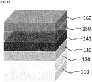
- FIG. 4 shows the structure of an organic solar cell or an organic light-emitting diode to which the organic thin film prepared according to the present disclosure is applied.
- examples and comparative examples are described referring to FIG. 4 .
- Comparative Example 1 Fabrication of organic solar cell by using spin coating method
- anode layer 120 transparent ITO having a sheet resistance of 15 ⁇ /sq and a thickness of -1,500 ⁇ was prepared on a glass substrate 110.
- the glass substrate on which the ITO anode layer was formed was ultrasonically washed with acetone and isopropyl alcohol for 15 minutes each and then dried. Then, the ITO substrate was surface-treated for 10 minutes using an atmospheric plasma surface-treating apparatus.
- PEDOT:PSS polyethylenedioxythiophene polystyrene sulfonate
- a photoactive layer 140 with a thickness of 100 nm was formed by spin-coating a solution prepared by dissolving 15 mg of regioregular poly(trihexylthiophene) (P3HT) as an electron donor and 12 mg of the fullerene derivative [6,6]-phenyl-C 61 -butyric acid methyl ether (PCBM) as an electron acceptor in 1 mL of chlorobenzene on the hole transport layer. Then, the substrate was dried at 50 °C for 40 minutes.
- P3HT regioregular poly(trihexylthiophene)
- PCBM fullerene derivative
- the substrate was dried at 50 °C for 40 minutes.
- the substrate was loaded in a vacuum deposition apparatus and an organic solar cell was obtained by forming lithium fluoride as a cathode layer of a counter electrode on the photoactive layer to a thickness of 0.5 nm and then forming an Al thin film with a thickness of 100 nm by vacuum deposition, thereby forming a double-layered cathode layer 150,160.
- the voltage-current density measurement result of the organic solar cell device fabricated by the spin coating method in Comparative Example 1 is shown in FIG. 6 .
- the V oc , J sc and FF of the fabricated organic solar cell were measured to be 0.62, 10.9 and 64.2%, respectively.
- the photovoltaic conversion rate was 4.4%.
- an organic solar cell was fabricated in the same manner as in Comparative Example 1, except that 10 ⁇ L of a solution prepared by dissolving 15 mg of P3HT and 12 mg of the fullerene derivative PCBM in 1 mL of chlorobenzene was dropped onto distilled water as a liquid substrate and an organic photoactive layer was formed by using the spontaneous spreadingeffect caused by the difference in surface tension between the two solutions and then transferred onto a hole transport layer.
- the V oc , J sc and FF of the fabricated organic solar cell were measured to be 0.67, 13.7 and 69%, respectively.
- the photovoltaic conversion rate was 6.3%.
- the voltage-current density measurement result is shown in FIG. 6 .
- An organic solar cell was fabricated in the same manner as in Comparative Example 1, except that ITO having a sheet resistance of 30 ⁇ /sq and a thickness of -1,500 ⁇ was prepared on a PEN substrate, 10 ⁇ L of a solution prepared by dissolving 10 mg of PTB7 and 15 mg of PC70BM in 1 mL of a 90:10 (v/v) solvent mixture of chlorobenzene and 1,8-diidooctane (DIO) was dropped onto distilled water as a liquid substrate and an organic photoactive layer was formed by using the spontaneous spreadingeffect caused by the difference in surface tension between the two solutions and then transferred onto a hole transport layer.
- ITO having a sheet resistance of 30 ⁇ /sq and a thickness of -1,500 ⁇ was prepared on a PEN substrate
- the V oc , J sc and FF of the fabricated organic solar cell were measured to be 0.75, 14.7 and 68%, respectively.
- the photovoltaic conversion rate was 7.3%.
- An organic solar cell was fabricated in the same manner as in Comparative Example 1, except that 15 ⁇ L of a solution prepared by dissolving 15 mg of PTB7 and 10 mg of the polyperylene derivative PNDI in 1 mL of a 99.5:0.5 (v/v) solvent mixture of chlorobenzene and 1,8-diidooctane (DIO) was dropped onto distilled water as a liquid substrate and an organic photoactive layer was formed by using the spontaneous spreading effect caused by the difference in surface tension between the two solutions and then transferred onto a hole transport layer.
- the V oc , J sc and FF of the fabricated organic solar cell were measured to be 0.81, 18.8 and 51%, respectively.
- the photovoltaic conversion rate was 7.7%.
- An organic solar cell was fabricated in the same manner as in Comparative Example 1, except that 10 ⁇ L of a solution prepared by dissolving 15 mg of PTB7-Th in a 95:5 (v/v) solvent mixture of chlorobenzene and 1,8-diidooctane (DIO) was dropped onto acetone as a liquid substrate, an electron donor layer was formed by using the spontaneous spreading effect caused by the difference in surface tension between the two solutions and then transferred onto a hole transport layer, 15 ⁇ L of a solution prepared by dissolving 10 mg of the polyperylene derivative PNDI in 1 mL of chloroform was dropped onto distilled water as a liquid substrate and an electron acceptor layer was formed and transferred onto the electron donor layer.
- a solution prepared by dissolving 15 mg of PTB7-Th in a 95:5 (v/v) solvent mixture of chlorobenzene and 1,8-diidooctane (DIO) was dropped onto acetone as a liquid substrate
- the V oc , J sc and FF of the fabricated organic solar cell were measured to be 0.79, 13.46 and 56%, respectively.
- the photovoltaic conversion rate was 5.96%.
- the voltage-current density measurement result of the device is shown in FIG. 7 .
- Comparative Example 2 Fabrication of organic/inorganic hybrid perovskite solar cell device by using spin coating method
- a glass substrate on which FTO having a sheet resistance of 20 ⁇ /sq was deposited as a cathode layer was ultrasonically washed with distilled water, acetone and isopropyl alcohol for 15 minutes each and then dried. Then, the FTO substrate was surface-treated for 10 minutes using an atmospheric plasma surface-treating apparatus.
- ZnO nanoparticles were spin-coated on the FTO cathode layer to a thickness of 40 nm as an electron transport layer.
- the substrate was dried at room temperature and transferred to a glovebox under a dry nitrogen atmosphere of 1 ppm or lower oxygen.
- a photoactive layer with a thickness of 270 nm was formed by coating a 1.2 M methylammonium lead triiodide (CH 3 NH 3 PbI 3 ) solution prepared by dissolving methylammonium iodide (CH 3 NH 3 I) and lead diiodide (PbI 2 ) in a 7:3 (v/v) solvent mixture of ⁇ -butyrolactone and dimethyl sulfoxide at a molar ratio of 1:1 and stirring at 60 °C for 12 hours on the electron transport layer. Then, the substrate was dried at 100 °C for 10 minutes.
- CH 3 NH 3 PbI 3 methylammonium lead triiodide
- PbI 2 lead diiodide
- a hole transport layer was formed by adding 13.6 ⁇ L of Li-bis(trifluoromethanesulfonyl)imide (Li-TFSI)/acetonitrile (28.3 mg/1 mL) and 6.8 ⁇ L of TBP to a poly(triarylamine) (PTAA) solution dissolved in toluene to 15 mg/mL and spin-coating the solution on the photoactive layer.
- Li-TFSI Li-bis(trifluoromethanesulfonyl)imide
- PTAA poly(triarylamine)
- An organic/inorganic hybrid perovskite solar cell was obtained by forming Ag thin film with a thickness of 100 nm as a cathode layer of a counter electrode on the photoactive layer by vacuum deposition.
- the voltage-current density measurement result of the organic/inorganic hybrid perovskite solar cell device fabricated by the spin coating method in Comparative Example 2 is shown in FIG. 8 .
- the V oc , J sc and FF of the fabricated organic solar cell were measured to be 0.94, 16.72 and 69%, respectively.
- the photovoltaic conversion rate was 10.16%.
- An organic/inorganic hybrid perovskite solar cell was fabricated in the same manner as in Comparative Example 1, except that 20 ⁇ L of a 1.2 M methylammonium lead triiodide (CH 3 NH 3 PbI 3 ) solution prepared by dissolving methylammonium iodide (CH 3 NH 3 I) and lead diiodide (PbI 2 ) in a 7:3 (v/v) solvent mixture of ⁇ -butyrolactone and dimethyl sulfoxide at a molar ratio of 1:1 and stirring at 60 °C for 12 hours was dropped on acetone as a liquid substrate and a photoactive layer was formed by using the spontaneous spreading effect caused by the difference in surface tension between the two solutions and then transferred onto a hole transport layer, which was then dried at 100 °C for 10 minutes.
- a methylammonium lead triiodide CH 3 NH 3 PbI 3
- the V oc , J sc and FF of the fabricated organic/inorganic hybrid perovskite solar cell were measured to be 0.89, 16.49 and 74%, respectively.
- the photovoltaic conversion rate was 10.91%.
- the voltage-current density measurement result of the device is shown in FIG. 8 .
- Comparative Example 3 Fabrication of polymer light-emitting diode by using spin coating method
- An organic light-emitting diode having a structure shown in FIG. 4 was fabricated.
- the photoactive layer 140 of Comparative Example 1 was replaced by a light-emitting layer 140.
- a PEDOT:PSS hole transport layer with a thickness of about 40 nm was formed on a PET/ITO substrate pretreated as in Comparative Example 1 using a spin coater. After heat treatment at 130 °C for 20 minutes, a solution in which a light-emitting polymer (Merck super yellow polymer, PDY-132) was dissolved in toluene to a concentration of 0.5 wt% was spin-coated on the hole transport layer to obtain a thin film with a thickness of 100 nm. The thin film was heat-treated at 90 °C for 30 minutes.
- a light-emitting polymer Merck super yellow polymer, PDY-132
- the substrate was loaded in a vacuum deposition apparatus and a polymer light-emitting diode was obtained by forming lithium fluoride as a cathode layer of a counter electrode on the light-emitting layer to a thickness of 0.5 nm and then forming an Al thin film with a thickness of 100 nm by vacuum deposition, thereby forming a double-layered cathode layer.
- a polymer light-emitting diode was fabricated in the same manner as in Comparative Example 3, except that 10 ⁇ L of a solution in which a light-emitting polymer (Merck super yellow polymer, PDY-132) was dissolved in toluene to a concentration of 0.5 wt% was dropped on distilled water as a liquid substrate and a light-emitting layer was formed by using the spontaneous spreading effect caused by the difference in surface tension between the two solutions and then transferred onto a hole transport layer.
- a light-emitting polymer Merck super yellow polymer, PDY-132
- a polymer light-emitting diode was fabricated in the same manner as in Comparative Example 3, except that methylammonium bromide and lead dibromide were dissolved in dimethyl sulfoxide at a molar ratio of 1:1 to a concentration of 10 wt%, methylammonium chloride and lead dichloride were similarly dissolved in dimethyl sulfoxide at a molar ratio of 1:1 to a concentration of 10 wt%, the two solutions were mixed at a volume ratio of 1:1, 20 ⁇ L of the mixture was dropped onto chloroform as a liquid substrate and a light-emitting layer was formed by using the spontaneous spreading effect caused by the difference in surface tension between the two solutions and then transferred onto a hole transport layer.
- An organic thin-film transistor having a structure shown in FIG. 5 was fabricated.
- a gate electrode 220 ITO was deposited on a polyethersulfone (PES) substrate 210 by pulsed laser deposition.
- a polymer gate insulation layer 230 was prepared by mixing 8 wt% PVP and 1.6 wt% MMF with a PGMEA solvent, dropping 20 ⁇ L of the PVP solution on IPA as a liquid substrate and forming a thin film by using the spontaneous spreading effect caused by the difference in surface tension between the two solutions and then transferred onto the ITO electrode.
- the substrate was heat-treated on a hot plate at 90 °C for 90 seconds inside a glovebox under a nitrogen atmosphere and then treated with UV and ozone for 10 minutes.
- the substrate was further heat-treated at 90 °C for 1 hour for curing and crosslinking of PVP.
- the surface of the insulation layer was treated with oxygen plasma, HMDS and OTS before forming a semiconductor layer 250.
- a pentacene layer with a thickness of 300 ⁇ was deposited by thermal evaporation at a pressure of 3.0x10 -7 Torr.
- An organic thin-film transistor was fabricated by depositing a source electrode 260 and a silver drain electrode 240 with a thickness of 100 nm on the semiconductor layer by thermal deposition using a shadow mask.
- the present disclosure relates to a method for forming a thin film on a liquid substrate by using the surface tension between the liquid substrate and a solution and allows for fabrication of an organic/inorganic electronic device including a high-performance organic solar cell with an effectively controlled nanomorphology.
- a large-area thin film can be formed effectively with little material loss and the process is very simple because the formed thin film can be transferred freely to a glass, plastic or metal substrate without limitation.
Landscapes
- Engineering & Computer Science (AREA)
- Chemical & Material Sciences (AREA)
- Materials Engineering (AREA)
- Manufacturing & Machinery (AREA)
- Physics & Mathematics (AREA)
- Optics & Photonics (AREA)
- Inorganic Chemistry (AREA)
- Electromagnetism (AREA)
- Photovoltaic Devices (AREA)
- Liquid Deposition Of Substances Of Which Semiconductor Devices Are Composed (AREA)
- Thin Film Transistor (AREA)
Abstract
Description
- The present disclosure provides a method for forming a thin film on a liquid substrate. Specifically, it relates to a method for forming an organic/inorganic thin film through the surface tension between a liquid substrate and a solution by supplying the solution to the liquid substrate.
- The fabrication of an organic/inorganic thin film is a fundamental technology in nanotechnology. It is a technology essential for most electronic devices such as mobile phones, military equipment, solar cells, etc., which need to be lightweight, thin and bendable.
- Vacuum deposition has been the representative technology for formation of an organic/inorganic thin film since the mid-20th century. There has been a lot of advancement focused on electronic materials and many methods have been proposed. The vacuum deposition techniques include physical deposition and chemical deposition methods. And the wet deposition techniques include electro-plating, spin coating, slot-die coating, etc.
- High-performance electronic devices using organic/inorganic thin films are being researched actively around the world. Also in the industry, investments are being made consistently in the development of new technology for productivity improvement and cost reduction because the organic/inorganic thin film formation is a fundamental technology in electronic devices such as semiconductors, displays and solar cells. In the light of this global trend, it is expected that the investment will be expanded further and competitions for breakthrough thin film formation technologies that can produce thinner and cost-effective devices will become more increasingly fierce.
- Organic solar cells can be given as an example of the reason why a new technology for forming organic thin films is necessary. The organic solar is drawing attentions as a next-generation solar cell because it can be produced at low cost and is light and flexible. With low price and light weight, it is applicable to most fields where energy harvesting is necessary, such as batteries for mobile phones, military equipment, etc.
- Despite the high marketability and applicability, there is an obstacle to the commercialization of the organic solar cell considered as the next-generation energy source due to the difficulties in large-scale process and the R2R (roll-to-roll) process. Although many researches are being conducted on processes for large-scale process, it is difficult to fabricate large area organic solar cells with high efficiency due to the difficulty in the control of nanomorphology over a large area.
- Although the spin coating method has been considered the most effective method for fabricating high-efficiency organic solar cells capable of controlling nanomorphology, it is disadvantageous in that it is inappropriate for commercialization because it is impossible to achieve large-area thin film. Although large-area thin film can be achieved with many thin film forming methods such as doctor blading, slot-die coating, etc., it is difficult to fabricate high-efficiency organic solar cells due to the difficulty in forming uniform thin films because they are very sensitive to such factors as ink composition, interaction between the ink and the surface, etc.
- Reference can be made to Korean Patent Registration No.
10-1189172 (Oct. 10, 2012 - (Patent document 1)
KR 10-1189172 B - The present disclosure is directed to providing a method for forming a uniform single-layer or multi-layer organic/inorganic thin film with improved air-stability very quickly and effectively on a liquid substrate with little material loss by using the difference in surface tension between solutions.
- An ultra-fast method for forming an organic/inorganic thin film by using a spontaneous spreading effect according to the present disclosure includes: a step of preparing a solution by dissolving one or more organic/inorganic material in a solvent; a step of forming an organic/inorganic thin film by supplying the prepared solution onto a liquid substrate; and a step of transferring the formed thin film to a substrate, wherein, in the step of forming the organic/inorganic thin film, the organic/inorganic material forms the thin film on the liquid substrate through a spontaneous spreading phenomenon caused by a difference in surface tension between the liquid substrate and the solution and through evaporation of the solvent and a dissolution process of the solvent to the liquid substrate.
- In the step of forming the organic/inorganic thin film, a single-layer or multi-layer thin film is formed on the liquid substrate by a solution wherein a single or composite organic/inorganic material is dissolved in a solvent.
- The organic/inorganic material includes one or more of an organic compound including a conjugated polymer or a conjugated small molecule such as a polybenzothiophene derivative, a polythiophene derivative, a poly(p-phenylene) derivative, a polyfluorene derivative, a polyacetylene derivative, a polypyrrole derivative, a polyvinylcarbazole derivative, a polyaniline derivative and a polyphenylenevinylene derivative, an n-type polymer compound such as a polyperylene derivative, a fullerene derivative such as fullerene (C60), [6,6]-phenyl-C61-butyric acid methyl ether (PCBM), [6,6]-phenyl-C71-butyric acid methyl ether (PC70BM), an inorganic/organic hybrid perovskite compound of a perovskite structure containing an amidinium ion and an organic ammonium ion as monovalent organic cations, a divalent metal ion as an inorganic cation and a halogen ion as an anion, or an inorganic semiconductor quantum dot compound selected from CdS, CdSe, CdTe, PbS, PbSe, PbSxSei-x (0 < x < 1), Bi2S3, Bi2Se3, InP, InCuS2, In(CuGa)Se2, Sb2S3, Sb2Se3, SnSx (1 ≤ x ≤ 2), NiS, CoS, FeSx (1 ≤ x ≤ 2), In2S3, MoS and MoSe.
- The liquid substrate is one having a higher surface tension than the solvent, selected from a group consisting of distilled water, glycerol, formamide and ethylene glycol.
- The solvent is one capable of dissolving the organic/inorganic material and having a difference in surface tension with the liquid substrate such that a spontaneous spreading effect can occur, selected from a group consisting of chlorobenzene, chloroform, toluene and dichlorobenzene.
- The substrate to which the organic/inorganic thin film is transferred is one of a flexible polymer substrate, a metal substrate and a glass substrate.
- The flexible polymer substrate is one selected from a group consisting of polydimethylsiloxane (PDMS), polyethylene terephthalate (PET), polyethylene naphthalate (PEN) polyethylene (PE), polyethersulfone (PES), polycarbonate (PC), polyarylate (PAR) and polyimide (PI).
- The metal substrate is one selected from a group consisting of SUS (steel use stainless), aluminum, steel and copper.
- The present disclosure provides an organic/inorganic thin film prepared by the method for forming an organic/inorganic thin film described above.
- The present disclosure provides an organic/inorganic electronic device containing the organic/inorganic thin film.
- The organic/inorganic electronic device is one of a solar cell, a light-emitting diode and a transistor.
- The present disclosure relates to a method for forming an organic/inorganic thin film on a liquid substrate by using the surface tension between the liquid substrate and a solution and allows for fabrication of an organic/inorganic electronic device including a solar cell, a light-emitting diode, a thin-film transistor, etc.
- According to the present disclosure, a uniform organic/inorganic thin film can be formed very quickly and effectively with little material loss and the process is very simple because the formed thin film can be transferred freely to a glass, plastic or metal substrate without additional treatment.
- In addition, the present disclosure can improve the efficiency of an organic/inorganic electronic device because the nanomorphology of the thin film can be controlled effectively during the crystallization, orientation and phase separation of materials.
- Also, in the present disclosure, the organic/inorganic solution used for spin coating can be utilized without modification. That is to say, the present disclosure solves the problems occurring during thin film formation by the conventional spin coating method that about 90% or more material is lost and it is difficult to attain a uniform thin film because a lot of time is required for optimization due to high sensitivity to such factors as ink composition, interaction between the ink and the surface, etc.
- In addition, the present disclosure allows for effective formation of a multi-layer thin film without limitation to solvent or material. When a multi-layer thin film is formed by the spin coating method, there is a limitation that a solvent which does not dissolves the thin film of the lower layer has to be used. In contrast, according to the present disclosure, a multi-layer thin film can be prepared from various materials because the formed thin film can be transferred freely.
- Whereas the existing thin film formation method such as spin coating is limited in that the process should be conducted under a nitrogen atmosphere because of change in material characteristics due to oxygen or water, the present disclosure can ensure the atmospheric stability of the thin film material because the thin film is formed very quickly. In addition, price competitiveness can be ensured because an organic/inorganic electronic device can be fabricated under an air atmosphere.
- The present disclosure can save the time and cost required for the formation and transfer of a thin film and can improve price competitiveness in the manufacturing of solar cells, light-emitting diodes and transistors.
- In addition, it is applicable to wearable flexible organic/inorganic electronic devices requiring flexibility and low cost because it allows various substrates to be used.
-
-
FIG. 1 schematically shows an ultra-fast organic/inorganic thin film preparation and transfer process by using a spontaneous spreading effect according to the present disclosure. -
FIG. 2 shows increase and decrease of the thickness of a thin film formed by spontaneous spreading depending on the concentration and amount of a solution, the size of a container and the number of transferred thin films. -
FIG. 3 shows that an organic/inorganic thin film is transferred regardless of the type or shape of a target substrate. -
FIG. 4 shows the structure of an organic solar cell or an organic light-emitting diode to which an organic thin film prepared according to the present disclosure is applied. -
FIG. 5 shows the structure of an organic thin-film transistor to which an organic thin film prepared according to the present disclosure is applied. -
FIG. 6 shows the current-voltage curve of an organic solar cell fabricated in Example 1 and Comparative Example 1. -
FIG. 7 shows the current-voltage curve of an organic solar cell fabricated in Example 4. -
FIG. 8 shows the current-voltage curve of an organic/inorganic hybrid solar cell fabricated in Example 5 and Comparative Example 2. - Hereinafter, the exemplary embodiments of the present disclosure will be described in detail with reference to the attached drawings. However, the present disclosure is not limited by the exemplary embodiments described below but may be embodied in various ways. The exemplary embodiments are provided so that the description of the present disclosure is complete and the scope of the present disclosure is completely conveyed to those of ordinary skill. In the drawings, like numerals refer to like elements.
- The present disclosure provides a method for forming a thin film with a nanomorphology effectively controlled during crystallization, phase separation, etc. without the loss of a supplied solution by using the spontaneous spreading phenomenon on a liquid substrate, with minimized modification of the existing organic/inorganic solution for spin coating and allows for fabrication of a high-efficiency organic electronic device at low cost.
- The method of the present disclosure includes a step of preparing a solution by dissolving one or more organic/inorganic material in a solvent and a step of forming an organic/inorganic thin film by supplying the prepared solution onto a liquid substrate. The present disclosure provides a method for forming the layers of an organic/inorganic electronic device by using the spontaneous spreading phenomenon.
- An ultra-fast method for forming and transferring a large-area organic/inorganic thin film by using the spontaneous spreading effect is described referring to
FIG. 1 . - First, a
solution 30 is formed before thesolution 30 is supplied onto aliquid substrate 20 accommodated in acontainer 10. - The
solution 30 is prepared by adding one or more organic/inorganic material to a solvent and dissolving sufficiently under an inert gas condition. If necessary, the nanomorphology can be controlled by further adding an additive. The organic/inorganic material added to the solvent is dissolved in the solvent to form the solution and is used in the finally fabricated organic/inorganic thin-film device. The solvent may be used to dissolve an organic material and has the property of spreading on theliquid substrate 20. - For example, the organic/inorganic material added to the solvent may be one or more of an organic compound including a conjugated polymer or a conjugated small molecule such as a polybenzothiophene derivative, a polythiophene derivative, a poly(p-phenylene) derivative, a polyfluorene derivative, a polyacetylene derivative, a polypyrrole derivative, a polyvinylcarbazole derivative, a polyaniline derivative and a polyphenylenevinylene derivative, an n-type polymer compound such as a polyperylene derivative, a fullerene derivative such as fullerene (C60), [6,6]-phenyl-C61-butyric acid methyl ether (PCBM), [6,6]-phenyl-C71-butyric acid methyl ether (PC70BM), an inorganic/organic hybrid perovskite compound of a perovskite structure containing an amidinium ion and an organic ammonium ion as monovalent organic cations, a divalent metal ion as an inorganic cation and a halogen ion as an anion, or an inorganic semiconductor quantum dot compound selected from CdS, CdSe, CdTe, PbS, PbSe, PbSxSei-x (0 < x < 1), Bi2S3, Bi2Se3, InP, InCuS2, In(CuGa)Se2, Sb2S3, Sb2Se3, SnSx (1 ≤ x ≤ 2), NiS, CoS, FeSx (1 ≤ x ≤ 2), In2S3, MoS and MoSe, although not being limited thereto.
- For example, the liquid substrate may be a solvent which does not dissolve the organic/inorganic material and has a higher surface tension than the solvent, including distilled water, glycerol, formamide, ethylene glycol, etc.
- For example, the solvent may be a solvent which dissolves the organic/inorganic material and has a difference in surface tension with the liquid substrate such that a spontaneous spreading effect can occur, including chlorobenzene, chloroform, toluene, dichlorobenzene, etc.
-
FIG. 1 shows that, due to the surface tension between theliquid substrate 20 and thesolution 30, a polymer which is an organic material spreads thinly on theliquid substrate 20 through evaporation and dissolution of the solvent. That is to say, the spontaneous spreading of the organic/inorganic solution 30 occurs due to the difference in the surface tension with theliquid substrate 20 and the solvent is evaporated into the air and, at the same time, is dissolved into the liquid substrate during the diffusion. - Next, a step of forming a thin film on the
liquid substrate 20 by using the formedsolution 30 is described referring toFIG. 1 . Theliquid substrate 20 may be a liquid which has a high surface tension and does not dissolve the organic/inorganic material, such as water. - In
FIG. 1 , I through IV show a process whereby an organic/inorganic thin film is transferred from thesolution 30 supplied onto theliquid substrate 20. - Specifically, I and II of
FIG. 1 show the step of forming a thin film. A trace amount of thesolution 30 is added dropwise to theliquid substrate 20 under an air atmosphere at room temperature using apipette 40 or a syringe and is allowed to stand until the solvent dissolving the organic/inorganic material is completely dissolved into theliquid substrate 20 or evaporated into the air. - III and IV of
FIG. 1 show the step of separating and transferring the thin film. Atarget substrate 50 to which the organic/inorganic thin film is to be transferred is lowered vertically toward theliquid substrate 20 such that it contacts with the upper side of the organic/inorganic thin film from which all the solvent contained in thesolution 30 has evaporated. During this process, the organic/inorganic thin film is transferred as soon as it contacts with thetarget substrate 50. If thetarget substrate 50 is lifted vertically from theliquid substrate 20, the organic/inorganic thin film is separated from theliquid substrate 20 and the transfer is completed. - For example, the
liquid substrate 20 may be a solvent which does not dissolve the organic/inorganic material and has a higher surface tension than the solvent, including distilled water, glycerol, formamide, ethylene glycol, etc. - Hereinafter, the present disclosure will be described in detail through a test example and examples.
- However, the following test example and examples are for illustrative purposes only and the scope of the present disclosure is not limited by the examples.
- 10 µL of a solution of PTB7:PC71 BM in chlorobenzene was added dropwise onto 50 mL of water held in a Petri dish with a diameter of 10 cm at room temperature under an air atmosphere. A thin film was formed within 10 seconds as the organic solvent was completely dried.
-
FIG. 2 shows the change in the thickness of the organic thin film due to spontaneous spreading. - Specifically,
FIG. 2 shows the increase and decrease of the thickness of the thin film depending on the concentration and amount of the solution, the size of the container holding the water and the number of transferred thin films. That is to say, the figure shows increase and decrease of the thickness of the organic thin film formed through spontaneous spreading depending on the concentration and amount of the solution, the size of the container holding the water and the number of transferred thin films. - It can be seen that the thickness of the organic thin film increases with the concentration and amount of the solution and the number of transferred thin films and decreases with the size of the container holding the water.
- Because the size of the formed thin film can be controlled by varying the size of the container (bath), it is possible to obtain a large-area thin film having uniform properties.
-
FIG. 3 shows that the organic/inorganic thin film is transferred regardless of the type or shape of a target substrate. - Specifically,
FIG. 3 shows that the organic/inorganic thin film is transferred to target substrates formed of PDMS (a), PET (b), paper (c) and glass (d). It can be seen that the transfer is achieved as desired regardless of the type or shape of the target substrate. -
FIG. 4 shows the structure of an organic solar cell or an organic light-emitting diode to which the organic thin film prepared according to the present disclosure is applied. Hereinafter, examples and comparative examples are described referring toFIG. 4 . - First, comparative examples are described referring to
FIG. 4 . - As an
anode layer 120, transparent ITO having a sheet resistance of 15 Ω/sq and a thickness of -1,500 Å was prepared on aglass substrate 110. The glass substrate on which the ITO anode layer was formed was ultrasonically washed with acetone and isopropyl alcohol for 15 minutes each and then dried. Then, the ITO substrate was surface-treated for 10 minutes using an atmospheric plasma surface-treating apparatus. - Then, as a
hole transport layer 130, polyethylenedioxythiophene polystyrene sulfonate (PEDOT:PSS) was spin-coated on the ITO anode layer to a thickness of 40 nm. The substrate was dried at 140 °C for 15 minutes and transferred to a glovebox under a dry nitrogen atmosphere of 1 ppm or lower oxygen. Then, aphotoactive layer 140 with a thickness of 100 nm was formed by spin-coating a solution prepared by dissolving 15 mg of regioregular poly(trihexylthiophene) (P3HT) as an electron donor and 12 mg of the fullerene derivative [6,6]-phenyl-C61-butyric acid methyl ether (PCBM) as an electron acceptor in 1 mL of chlorobenzene on the hole transport layer. Then, the substrate was dried at 50 °C for 40 minutes. - Next, the substrate was loaded in a vacuum deposition apparatus and an organic solar cell was obtained by forming lithium fluoride as a cathode layer of a counter electrode on the photoactive layer to a thickness of 0.5 nm and then forming an Al thin film with a thickness of 100 nm by vacuum deposition, thereby forming a double-layered cathode layer 150,160.
- The voltage-current density measurement result of the organic solar cell device fabricated by the spin coating method in Comparative Example 1 is shown in
FIG. 6 . - The Voc, Jsc and FF of the fabricated organic solar cell were measured to be 0.62, 10.9 and 64.2%, respectively. The photovoltaic conversion rate was 4.4%.
- Hereinafter, the examples of the present disclosure are described referring again to
FIG. 4 . - In this example, an organic solar cell was fabricated in the same manner as in Comparative Example 1, except that 10 µL of a solution prepared by dissolving 15 mg of P3HT and 12 mg of the fullerene derivative PCBM in 1 mL of chlorobenzene was dropped onto distilled water as a liquid substrate and an organic photoactive layer was formed by using the spontaneous spreadingeffect caused by the difference in surface tension between the two solutions and then transferred onto a hole transport layer.
- The Voc, Jsc and FF of the fabricated organic solar cell were measured to be 0.67, 13.7 and 69%, respectively. The photovoltaic conversion rate was 6.3%. The voltage-current density measurement result is shown in
FIG. 6 . - An organic solar cell was fabricated in the same manner as in Comparative Example 1, except that ITO having a sheet resistance of 30 Ω/sq and a thickness of -1,500 Å was prepared on a PEN substrate, 10 µL of a solution prepared by dissolving 10 mg of PTB7 and 15 mg of PC70BM in 1 mL of a 90:10 (v/v) solvent mixture of chlorobenzene and 1,8-diidooctane (DIO) was dropped onto distilled water as a liquid substrate and an organic photoactive layer was formed by using the spontaneous spreadingeffect caused by the difference in surface tension between the two solutions and then transferred onto a hole transport layer.
- The Voc, Jsc and FF of the fabricated organic solar cell were measured to be 0.75, 14.7 and 68%, respectively. The photovoltaic conversion rate was 7.3%.
- An organic solar cell was fabricated in the same manner as in Comparative Example 1, except that 15 µL of a solution prepared by dissolving 15 mg of PTB7 and 10 mg of the polyperylene derivative PNDI in 1 mL of a 99.5:0.5 (v/v) solvent mixture of chlorobenzene and 1,8-diidooctane (DIO) was dropped onto distilled water as a liquid substrate and an organic photoactive layer was formed by using the spontaneous spreading effect caused by the difference in surface tension between the two solutions and then transferred onto a hole transport layer.
- The Voc, Jsc and FF of the fabricated organic solar cell were measured to be 0.81, 18.8 and 51%, respectively. The photovoltaic conversion rate was 7.7%.
- An organic solar cell was fabricated in the same manner as in Comparative Example 1, except that 10 µL of a solution prepared by dissolving 15 mg of PTB7-Th in a 95:5 (v/v) solvent mixture of chlorobenzene and 1,8-diidooctane (DIO) was dropped onto acetone as a liquid substrate, an electron donor layer was formed by using the spontaneous spreading effect caused by the difference in surface tension between the two solutions and then transferred onto a hole transport layer, 15 µL of a solution prepared by dissolving 10 mg of the polyperylene derivative PNDI in 1 mL of chloroform was dropped onto distilled water as a liquid substrate and an electron acceptor layer was formed and transferred onto the electron donor layer.
- The Voc, Jsc and FF of the fabricated organic solar cell were measured to be 0.79, 13.46 and 56%, respectively. The photovoltaic conversion rate was 5.96%. The voltage-current density measurement result of the device is shown in
FIG. 7 . - A glass substrate on which FTO having a sheet resistance of 20 Ω/sq was deposited as a cathode layer was ultrasonically washed with distilled water, acetone and isopropyl alcohol for 15 minutes each and then dried. Then, the FTO substrate was surface-treated for 10 minutes using an atmospheric plasma surface-treating apparatus.
- Then, ZnO nanoparticles were spin-coated on the FTO cathode layer to a thickness of 40 nm as an electron transport layer. The substrate was dried at room temperature and transferred to a glovebox under a dry nitrogen atmosphere of 1 ppm or lower oxygen. Then, a photoactive layer with a thickness of 270 nm was formed by coating a 1.2 M methylammonium lead triiodide (CH3NH3PbI3) solution prepared by dissolving methylammonium iodide (CH3NH3I) and lead diiodide (PbI2) in a 7:3 (v/v) solvent mixture of γ-butyrolactone and dimethyl sulfoxide at a molar ratio of 1:1 and stirring at 60 °C for 12 hours on the electron transport layer. Then, the substrate was dried at 100 °C for 10 minutes.
- Next, the substrate was loaded in a vacuum deposition apparatus and a hole transport layer was formed by adding 13.6 µL of Li-bis(trifluoromethanesulfonyl)imide (Li-TFSI)/acetonitrile (28.3 mg/1 mL) and 6.8 µL of TBP to a poly(triarylamine) (PTAA) solution dissolved in toluene to 15 mg/mL and spin-coating the solution on the photoactive layer. An organic/inorganic hybrid perovskite solar cell was obtained by forming Ag thin film with a thickness of 100 nm as a cathode layer of a counter electrode on the photoactive layer by vacuum deposition.
- The voltage-current density measurement result of the organic/inorganic hybrid perovskite solar cell device fabricated by the spin coating method in Comparative Example 2 is shown in
FIG. 8 . - The Voc, Jsc and FF of the fabricated organic solar cell were measured to be 0.94, 16.72 and 69%, respectively. The photovoltaic conversion rate was 10.16%.
- An organic/inorganic hybrid perovskite solar cell was fabricated in the same manner as in Comparative Example 1, except that 20 µL of a 1.2 M methylammonium lead triiodide (CH3NH3PbI3) solution prepared by dissolving methylammonium iodide (CH3NH3I) and lead diiodide (PbI2) in a 7:3 (v/v) solvent mixture of γ-butyrolactone and dimethyl sulfoxide at a molar ratio of 1:1 and stirring at 60 °C for 12 hours was dropped on acetone as a liquid substrate and a photoactive layer was formed by using the spontaneous spreading effect caused by the difference in surface tension between the two solutions and then transferred onto a hole transport layer, which was then dried at 100 °C for 10 minutes.
- The Voc, Jsc and FF of the fabricated organic/inorganic hybrid perovskite solar cell were measured to be 0.89, 16.49 and 74%, respectively. The photovoltaic conversion rate was 10.91%. The voltage-current density measurement result of the device is shown in
FIG. 8 . - An organic light-emitting diode having a structure shown in
FIG. 4 was fabricated. In this comparative example, thephotoactive layer 140 of Comparative Example 1 was replaced by a light-emittinglayer 140. - A PEDOT:PSS hole transport layer with a thickness of about 40 nm was formed on a PET/ITO substrate pretreated as in Comparative Example 1 using a spin coater. After heat treatment at 130 °C for 20 minutes, a solution in which a light-emitting polymer (Merck super yellow polymer, PDY-132) was dissolved in toluene to a concentration of 0.5 wt% was spin-coated on the hole transport layer to obtain a thin film with a thickness of 100 nm. The thin film was heat-treated at 90 °C for 30 minutes. The substrate was loaded in a vacuum deposition apparatus and a polymer light-emitting diode was obtained by forming lithium fluoride as a cathode layer of a counter electrode on the light-emitting layer to a thickness of 0.5 nm and then forming an Al thin film with a thickness of 100 nm by vacuum deposition, thereby forming a double-layered cathode layer.
- A polymer light-emitting diode was fabricated in the same manner as in Comparative Example 3, except that 10 µL of a solution in which a light-emitting polymer (Merck super yellow polymer, PDY-132) was dissolved in toluene to a concentration of 0.5 wt% was dropped on distilled water as a liquid substrate and a light-emitting layer was formed by using the spontaneous spreading effect caused by the difference in surface tension between the two solutions and then transferred onto a hole transport layer.
- A polymer light-emitting diode was fabricated in the same manner as in Comparative Example 3, except that methylammonium bromide and lead dibromide were dissolved in dimethyl sulfoxide at a molar ratio of 1:1 to a concentration of 10 wt%, methylammonium chloride and lead dichloride were similarly dissolved in dimethyl sulfoxide at a molar ratio of 1:1 to a concentration of 10 wt%, the two solutions were mixed at a volume ratio of 1:1, 20 µL of the mixture was dropped onto chloroform as a liquid substrate and a light-emitting layer was formed by using the spontaneous spreading effect caused by the difference in surface tension between the two solutions and then transferred onto a hole transport layer.
- An organic thin-film transistor having a structure shown in
FIG. 5 was fabricated. - As a
gate electrode 220, ITO was deposited on a polyethersulfone (PES)substrate 210 by pulsed laser deposition. A polymergate insulation layer 230 was prepared by mixing 8 wt% PVP and 1.6 wt% MMF with a PGMEA solvent, dropping 20 µL of the PVP solution on IPA as a liquid substrate and forming a thin film by using the spontaneous spreading effect caused by the difference in surface tension between the two solutions and then transferred onto the ITO electrode. For removal of the solvent, the substrate was heat-treated on a hot plate at 90 °C for 90 seconds inside a glovebox under a nitrogen atmosphere and then treated with UV and ozone for 10 minutes. - Then, the substrate was further heat-treated at 90 °C for 1 hour for curing and crosslinking of PVP. In order to increase pentacene grain size and induce growth in the (001) direction, the surface of the insulation layer was treated with oxygen plasma, HMDS and OTS before forming a
semiconductor layer 250. A pentacene layer with a thickness of 300 Å was deposited by thermal evaporation at a pressure of 3.0x10⁻⁷ Torr. An organic thin-film transistor was fabricated by depositing asource electrode 260 and asilver drain electrode 240 with a thickness of 100 nm on the semiconductor layer by thermal deposition using a shadow mask. - As described above, the present disclosure relates to a method for forming a thin film on a liquid substrate by using the surface tension between the liquid substrate and a solution and allows for fabrication of an organic/inorganic electronic device including a high-performance organic solar cell with an effectively controlled nanomorphology.
- According to the present disclosure, a large-area thin film can be formed effectively with little material loss and the process is very simple because the formed thin film can be transferred freely to a glass, plastic or metal substrate without limitation.
- Those skilled in the art will appreciate that the conceptions and specific embodiments disclosed in the foregoing description may be readily utilized as a basis for modifying or designing other embodiments for carrying out the same purposes of the present disclosure. Those skilled in the art will also appreciate that such equivalent embodiments do not depart from the spirit and scope of the disclosure as set forth in the appended claims.
Claims (11)
- An ultra-fast method for formation of an organic/inorganic thin film by using a spontaneous spreading effect, comprising:a step of preparing a solution by dissolving one or more organic/inorganic material in a solvent;a step of forming an organic/inorganic thin film by supplying the prepared solution onto a liquid substrate; anda step of transferring the formed thin film to a substrate,wherein, in the step of forming the organic/inorganic thin film, the organic/inorganic material forms the thin film on the liquid substrate through a spontaneous spreading phenomenon caused by a difference in surface tension between the liquid substrate and the solution and through evaporation of the solvent and a dissolution process of the solvent to the liquid substrate.
- The ultra-fast method for formation of an organic/inorganic thin film by using a spontaneous spreading effect according to claim 1, wherein, in the step of forming the organic/inorganic thin film, a single-layer or multi-layer thin film is formed on the liquid substrate by a solution wherein a single or composite organic/inorganic material is dissolved in a solvent.
- The ultra-fast method for formation of an organic/inorganic thin film by using a spontaneous spreading effect according to claim 2, wherein the organic/inorganic material comprises one or more of an organic compound comprising a conjugated polymer or a conjugated small molecule such as a polybenzothiophene derivative, a polythiophene derivative, a poly(p-phenylene) derivative, a polyfluorene derivative, a polyacetylene derivative, a polypyrrole derivative, a polyvinylcarbazole derivative, a polyaniline derivative and a polyphenylenevinylene derivative, an n-type polymer compound such as a polyperylene derivative, a fullerene derivative such as fullerene (C60), [6,6]-phenyl-C61-butyric acid methyl ether (PCBM), [6,6]-phenyl-C71-butyric acid methyl ether (PC70BM), an inorganic/organic hybrid perovskite compound of a perovskite structure comprising an amidinium ion and an organic ammonium ion as monovalent organic cations, a divalent metal ion as an inorganic cation and a halogen ion as an anion, or an inorganic semiconductor quantum dot compound selected from CdS, CdSe, CdTe, PbS, PbSe, PbSxSei-x (0 < x < 1), Bi2S3, Bi2Se3, InP, InCuS2, In(CuGa)Se2, Sb2S3, Sb2Se3, SnSx (1 ≤ x ≤ 2), NiS, CoS, FeSx (1 ≤ x ≤ 2), In2S3, MoS and MoSe.
- The ultra-fast method for formation of an organic/inorganic thin film by using a spontaneous spreading effect according to claim 2, wherein the liquid substrate is one having a higher surface tension than the solvent, selected from a group consisting of distilled water, glycerol, formamide and ethylene glycol.
- The ultra-fast method for formation of an organic/inorganic thin film by using a spontaneous spreading effect according to claim 2, wherein the solvent is one capable of dissolving the organic/inorganic material and having a difference in surface tension with the liquid substrate such that a spontaneous spreading effect can occur, selected from a group consisting of chlorobenzene, chloroform, toluene and dichlorobenzene.
- The ultra-fast method for formation of an organic/inorganic thin film by using a spontaneous spreading effect according to claim 1, wherein the substrate to which the organic/inorganic thin film is transferred is one of a flexible polymer substrate, a metal substrate and a glass substrate.
- The ultra-fast method for formation of an organic/inorganic thin film by using a spontaneous spreading effect according to claim 6, wherein the flexible polymer substrate is one selected from a group consisting of polydimethylsiloxane (PDMS), polyethylene terephthalate (PET), polyethylene naphthalate (PEN) polyethylene (PE), polyethersulfone (PES), polycarbonate (PC), polyarylate (PAR) and polyimide (PI).
- The ultra-fast method for formation of an organic/inorganic thin film by using a spontaneous spreading effect according to claim 6, wherein the metal substrate is one selected from a group consisting of SUS (steel use stainless), aluminum, steel and copper.
- An organic/inorganic thin film prepared by the method for preparing an organic/inorganic thin film by using a spontaneous spreading effect according to any of claims 1 to 8.
- An organic/inorganic electronic device comprising the organic/inorganic thin film according to claim 9.
- The organic/inorganic electronic device according to claim 10, wherein the organic/inorganic electronic device is one of a solar cell, a light-emitting diode and a transistor.
Applications Claiming Priority (2)
| Application Number | Priority Date | Filing Date | Title |
|---|---|---|---|
| KR1020150101194A KR101687491B1 (en) | 2015-07-16 | 2015-07-16 | Ultrafast formation and transfer of organic and inorganic thin-films utilizing spontaneous spreading effect |
| PCT/KR2016/005336 WO2017010674A1 (en) | 2015-07-16 | 2016-05-19 | Ultra-fast method for preparing organic/organic thin film by using self-diffusion effects |
Publications (2)
| Publication Number | Publication Date |
|---|---|
| EP3324456A1 true EP3324456A1 (en) | 2018-05-23 |
| EP3324456A4 EP3324456A4 (en) | 2019-03-27 |
Family
ID=57735610
Family Applications (1)
| Application Number | Title | Priority Date | Filing Date |
|---|---|---|---|
| EP16824591.8A Withdrawn EP3324456A4 (en) | 2015-07-16 | 2016-05-19 | ULTRA-RAPID PROCESS FOR PREPARING ORGANIC / ORGANIC THIN LAYER USING SELF-DISPENSING EFFECTS |
Country Status (4)
| Country | Link |
|---|---|
| US (1) | US10580983B2 (en) |
| EP (1) | EP3324456A4 (en) |
| KR (1) | KR101687491B1 (en) |
| WO (1) | WO2017010674A1 (en) |
Families Citing this family (11)
| Publication number | Priority date | Publication date | Assignee | Title |
|---|---|---|---|---|
| WO2020152610A1 (en) * | 2019-01-23 | 2020-07-30 | Ahdieh Amjadi | Composite polymer/perovskite quantum dots luminescent material |
| KR102272548B1 (en) | 2019-08-08 | 2021-07-05 | 고려대학교 산학협력단 | A perovskite photoelectric device and manufacturing method thereof |
| CN110669235A (en) * | 2019-09-30 | 2020-01-10 | 北京工业大学 | A kind of convenient preparation method of PDMS thin film |
| KR102456930B1 (en) * | 2020-09-17 | 2022-10-21 | 한국전력공사 | Method for making large area carrier transport layer on liquid substrate and Method for transferring the carrier transport layer |
| CN113061285B (en) * | 2021-02-26 | 2021-10-22 | 中国科学院深圳先进技术研究院 | A kind of preparation method of ultra-thin porous stretchable film electrode |
| CN113644202B (en) * | 2021-08-05 | 2023-10-20 | 电子科技大学 | Organic solar cell prepared by spontaneous orientation film forming method and preparation method thereof |
| CN114907373B (en) * | 2022-05-31 | 2024-08-20 | 深圳先进电子材料国际创新研究院 | Conjugated organic small molecular material and preparation method and application thereof |
| CN116063716B (en) * | 2023-02-21 | 2023-09-01 | 上海懿禾嘉朋新材料科技有限公司 | Preparation method of flexible continuous defect-free MOF film |
| CN116528636A (en) * | 2023-03-13 | 2023-08-01 | 哈尔滨工业大学(深圳) | Planar self-powered light detector device based on micro-capacitance array and preparation method thereof |
| CN116528638A (en) * | 2023-03-29 | 2023-08-01 | 北京大学深圳研究生院 | Preparation method of active layer, narrow-band near-infrared photodiode and preparation method thereof |
| CN116496523A (en) * | 2023-05-22 | 2023-07-28 | 季华实验室 | A kind of high crystallinity ultra-thin polymer film and preparation method thereof |
Family Cites Families (13)
| Publication number | Priority date | Publication date | Assignee | Title |
|---|---|---|---|---|
| FR2818009B1 (en) * | 2000-12-07 | 2003-03-28 | Teherani Ferechteh Hosseini | PROCESS FOR PRODUCING A PROHIBITED BROADBAND SEMICONDUCTOR |
| US7777303B2 (en) * | 2002-03-19 | 2010-08-17 | The Regents Of The University Of California | Semiconductor-nanocrystal/conjugated polymer thin films |
| AU2003268487A1 (en) * | 2002-09-05 | 2004-03-29 | Nanosys, Inc. | Nanocomposites |
| CN1694791B (en) * | 2002-11-12 | 2010-08-18 | 大赛璐化学工业株式会社 | Porous membrane and method for producing same |
| FR2873492B1 (en) * | 2004-07-21 | 2006-11-24 | Commissariat Energie Atomique | PHOTOACTIVE NANOCOMPOSITE AND METHOD OF MANUFACTURING THE SAME |
| KR101174391B1 (en) * | 2004-08-27 | 2012-08-16 | 국립대학법인 홋가이도 다이가쿠 | Process for production of submicrohoneycomb structures |
| JP4341579B2 (en) * | 2005-05-19 | 2009-10-07 | セイコーエプソン株式会社 | Microlens manufacturing method |
| JP5276344B2 (en) * | 2008-03-26 | 2013-08-28 | 大日本スクリーン製造株式会社 | Substrate processing method and substrate processing apparatus |
| KR20100031036A (en) * | 2008-09-11 | 2010-03-19 | 포항공과대학교 산학협력단 | A manufacturing method of a thin film organic semiconductor using a phase seperation of blend of organic semiconductor/insulating polymer and organic thin film transister |
| US20110139183A1 (en) * | 2009-12-11 | 2011-06-16 | Katrina Mikhaylichenko | System and method of preventing pattern collapse using low surface tension fluid |
| KR101189172B1 (en) | 2010-12-16 | 2012-10-10 | 한국기계연구원 | Spray coating apparatus for organic solar cell, and the organic solar cell thereby |
| KR101288622B1 (en) * | 2011-03-04 | 2013-07-19 | 동아대학교 산학협력단 | Semiconductor layer generating Method of Organic Thin Film Transistor, OTFT generated by the Method, Display element generated by the OTFT, and Display Device generated by the Display element |
| US9416456B1 (en) * | 2011-05-20 | 2016-08-16 | University Of South Florida | Nano-hybrid structured regioregular polyhexylthiophene (RRPHTh) blend films for production of photoelectrochemical energy |
-
2015
- 2015-07-16 KR KR1020150101194A patent/KR101687491B1/en not_active Expired - Fee Related
-
2016
- 2016-05-19 US US15/744,137 patent/US10580983B2/en active Active
- 2016-05-19 WO PCT/KR2016/005336 patent/WO2017010674A1/en not_active Ceased
- 2016-05-19 EP EP16824591.8A patent/EP3324456A4/en not_active Withdrawn
Also Published As
| Publication number | Publication date |
|---|---|
| WO2017010674A1 (en) | 2017-01-19 |
| KR101687491B1 (en) | 2016-12-16 |
| US10580983B2 (en) | 2020-03-03 |
| US20180212148A1 (en) | 2018-07-26 |
| EP3324456A4 (en) | 2019-03-27 |
Similar Documents
| Publication | Publication Date | Title |
|---|---|---|
| US10580983B2 (en) | Ultra-fast method for formation of organic/inorganic thin film by using spontaneous spreading effect | |
| US9859515B2 (en) | Methods for producing thin film charge selective transport layers | |
| US7713779B2 (en) | Photoactive nanocomposite and method for the production thereof | |
| US9076768B2 (en) | Systems and methods for producing low work function electrodes | |
| Zhao et al. | Application of biuret, dicyandiamide, or urea as a cathode buffer layer toward the efficiency enhancement of polymer solar cells | |
| CN102509769B (en) | Thin-film photoelectric conversion devices based on hybridization of Ag2S flake nanocrystal arrays and P3HT prepared at low temperature | |
| Im et al. | Improved stability of interfacial energy-level alignment in inverted planar perovskite solar cells | |
| CN106256029A (en) | Organic solar cell and manufacturing method thereof | |
| WO2012106119A1 (en) | Photovoltaic cells | |
| Yu et al. | Optimization of the energy level alignment between the photoactive layer and the cathode contact utilizing solution-processed hafnium acetylacetonate as buffer layer for efficient polymer solar cells | |
| KR101282564B1 (en) | Modified PEDOT:PSS with Organic Solvent And Organic Solar Cells using It | |
| KR20200020346A (en) | The method for forming perovskite photoactive layer by in-line continuously coating and the apparatus for roll in-line continuously coating | |
| US11205753B2 (en) | Use of sequential processing for highly efficient organic solar cells based on conjugated polymers with temperature dependent aggregation | |
| CN113644202A (en) | A kind of organic solar cell prepared by spontaneous directional film formation method and preparation method thereof | |
| KR20180035057A (en) | Organic photovoltaics and method for manufacturing the same | |
| Inaba et al. | Eco-Friendly Push-Coated Polymer Solar Cells with No Active Material Wastes Yield Power Conversion Efficiencies over 5.5% | |
| Ko et al. | Ultrathin Poly (3-hexylthiophene) Nanowires as Chemically Robust and Versatile Surface Passivators of Perovskite Solar Absorbers | |
| Ciceroni et al. | Graphene oxide for DSSC, OPV and perovskite stability | |
| KR101316237B1 (en) | Manufacturing Method of Solution-processed semiconductor buffer layer And solar cells using it | |
| KR100822356B1 (en) | Manufacturing method of organic based solar cell inducing molecular arrangement using brush | |
| Yasuda et al. | Air-stable triarylamine-based amorphous polymer as donor material for bulk-heterojunction organic solar cells | |
| WO2015025333A1 (en) | Multilayer solar cell | |
| KR102540686B1 (en) | Method for producing perovskite compound powder | |
| Candan et al. | P3HT: PCBM Fotoaktif Tabanlı Tersine Çevrilmiş Polimer Güneş Hücrelerinin Üretimi ve Karakterizasyonu | |
| Raj | Heterojunction Perovskite Solar Cells |
Legal Events
| Date | Code | Title | Description |
|---|---|---|---|
| STAA | Information on the status of an ep patent application or granted ep patent |
Free format text: STATUS: THE INTERNATIONAL PUBLICATION HAS BEEN MADE |
|
| PUAI | Public reference made under article 153(3) epc to a published international application that has entered the european phase |
Free format text: ORIGINAL CODE: 0009012 |
|
| STAA | Information on the status of an ep patent application or granted ep patent |
Free format text: STATUS: REQUEST FOR EXAMINATION WAS MADE |
|
| 17P | Request for examination filed |
Effective date: 20180215 |
|
| AK | Designated contracting states |
Kind code of ref document: A1 Designated state(s): AL AT BE BG CH CY CZ DE DK EE ES FI FR GB GR HR HU IE IS IT LI LT LU LV MC MK MT NL NO PL PT RO RS SE SI SK SM TR |
|
| AX | Request for extension of the european patent |
Extension state: BA ME |
|
| DAV | Request for validation of the european patent (deleted) | ||
| DAX | Request for extension of the european patent (deleted) | ||
| A4 | Supplementary search report drawn up and despatched |
Effective date: 20190222 |
|
| RIC1 | Information provided on ipc code assigned before grant |
Ipc: H01L 51/00 20060101AFI20190218BHEP Ipc: B05D 1/20 20060101ALI20190218BHEP |
|
| STAA | Information on the status of an ep patent application or granted ep patent |
Free format text: STATUS: EXAMINATION IS IN PROGRESS |
|
| 17Q | First examination report despatched |
Effective date: 20210902 |
|
| STAA | Information on the status of an ep patent application or granted ep patent |
Free format text: STATUS: THE APPLICATION IS DEEMED TO BE WITHDRAWN |
|
| 18D | Application deemed to be withdrawn |
Effective date: 20220113 |