EP3324344B1 - Digitale elektronische schaltung und system zum implementieren eines gepulsten neuronalen netzes zur durchführung von unüberwachten nachweisen von mustern - Google Patents
Digitale elektronische schaltung und system zum implementieren eines gepulsten neuronalen netzes zur durchführung von unüberwachten nachweisen von mustern Download PDFInfo
- Publication number
- EP3324344B1 EP3324344B1 EP17305186.3A EP17305186A EP3324344B1 EP 3324344 B1 EP3324344 B1 EP 3324344B1 EP 17305186 A EP17305186 A EP 17305186A EP 3324344 B1 EP3324344 B1 EP 3324344B1
- Authority
- EP
- European Patent Office
- Prior art keywords
- signal
- input
- digital
- binary
- neuron
- Prior art date
- Legal status (The legal status is an assumption and is not a legal conclusion. Google has not performed a legal analysis and makes no representation as to the accuracy of the status listed.)
- Active
Links
Images



Classifications
-
- G—PHYSICS
- G06—COMPUTING OR CALCULATING; COUNTING
- G06N—COMPUTING ARRANGEMENTS BASED ON SPECIFIC COMPUTATIONAL MODELS
- G06N3/00—Computing arrangements based on biological models
- G06N3/02—Neural networks
- G06N3/04—Architecture, e.g. interconnection topology
- G06N3/049—Temporal neural networks, e.g. delay elements, oscillating neurons or pulsed inputs
-
- G—PHYSICS
- G06—COMPUTING OR CALCULATING; COUNTING
- G06F—ELECTRIC DIGITAL DATA PROCESSING
- G06F18/00—Pattern recognition
- G06F18/20—Analysing
- G06F18/21—Design or setup of recognition systems or techniques; Extraction of features in feature space; Blind source separation
- G06F18/214—Generating training patterns; Bootstrap methods, e.g. bagging or boosting
- G06F18/2148—Generating training patterns; Bootstrap methods, e.g. bagging or boosting characterised by the process organisation or structure, e.g. boosting cascade
-
- G—PHYSICS
- G06—COMPUTING OR CALCULATING; COUNTING
- G06F—ELECTRIC DIGITAL DATA PROCESSING
- G06F18/00—Pattern recognition
- G06F18/20—Analysing
- G06F18/21—Design or setup of recognition systems or techniques; Extraction of features in feature space; Blind source separation
- G06F18/217—Validation; Performance evaluation; Active pattern learning techniques
- G06F18/2178—Validation; Performance evaluation; Active pattern learning techniques based on feedback of a supervisor
-
- G—PHYSICS
- G06—COMPUTING OR CALCULATING; COUNTING
- G06F—ELECTRIC DIGITAL DATA PROCESSING
- G06F18/00—Pattern recognition
- G06F18/20—Analysing
- G06F18/22—Matching criteria, e.g. proximity measures
-
- G—PHYSICS
- G06—COMPUTING OR CALCULATING; COUNTING
- G06N—COMPUTING ARRANGEMENTS BASED ON SPECIFIC COMPUTATIONAL MODELS
- G06N3/00—Computing arrangements based on biological models
- G06N3/02—Neural networks
- G06N3/06—Physical realisation, i.e. hardware implementation of neural networks, neurons or parts of neurons
- G06N3/063—Physical realisation, i.e. hardware implementation of neural networks, neurons or parts of neurons using electronic means
-
- G—PHYSICS
- G06—COMPUTING OR CALCULATING; COUNTING
- G06N—COMPUTING ARRANGEMENTS BASED ON SPECIFIC COMPUTATIONAL MODELS
- G06N3/00—Computing arrangements based on biological models
- G06N3/02—Neural networks
- G06N3/08—Learning methods
- G06N3/088—Non-supervised learning, e.g. competitive learning
-
- G—PHYSICS
- G06—COMPUTING OR CALCULATING; COUNTING
- G06V—IMAGE OR VIDEO RECOGNITION OR UNDERSTANDING
- G06V20/00—Scenes; Scene-specific elements
- G06V20/40—Scenes; Scene-specific elements in video content
- G06V20/41—Higher-level, semantic clustering, classification or understanding of video scenes, e.g. detection, labelling or Markovian modelling of sport events or news items
-
- G—PHYSICS
- G06—COMPUTING OR CALCULATING; COUNTING
- G06V—IMAGE OR VIDEO RECOGNITION OR UNDERSTANDING
- G06V20/00—Scenes; Scene-specific elements
- G06V20/40—Scenes; Scene-specific elements in video content
- G06V20/44—Event detection
Definitions
- the invention relates to a digital electronic circuit and system for performing unsupervised detection of repeating patterns in a series of events. It belongs to the technical fields of digital electronics and machine learning, and more particularly to the sub-field of hardware-implemented neural networks. It lends itself to several applications including - but not limited to - video stream processing (e.g. Dynamic Vision Sensors) and audio processing (e.g. artificial cochleae).
- video stream processing e.g. Dynamic Vision Sensors
- audio processing e.g. artificial cochleae
- STDP spike-timing-dependent plasticity
- WO 2012/054109 discloses an artificial neural network having a plurality of synapses, each synapses having an adjustable weight which takes discrete values and changes in discrete steps with a probability depending on a time elapsed between a pair of spikes originating from a post-synaptic neuron circuit and a pre-synaptic neuron circuit connected to it.
- Operating such an artificial neural network is computationally intensive, as updating the synapses weights (essential for learning) requires multiply-accumulate operations, and multiplications are known to be the most space and power-hungry operations in the digital implementation of artificial neural networks.
- WO2013119867 discloses an artificial neural network wherein synapses do not have weights - or, equivalently, have binary weights: a synapse is then either existing or non-existing. Despite this simplification, operating this artificial neural network remains computationally intensive, as it requires measuring and applying variable delays to input and output spikes.
- artificial neural networks generally suffer from a lack of robustness: they may fail to detect a pattern it if is slightly distorted, or if the event acquisition rates varies.
- spiking neural networks are most often implemented by software running on general or specialized (e.g. graphical processing units, GPU).
- general or specialized e.g. graphical processing units, GPU.
- hardware implementations - based e.g. on FPGA (Field Programmable Gate Array) or other programmable circuits, or even on ASICs (Application Specific Integrated Circuit) - are used to improve performances.
- FPGA Field Programmable Gate Array
- ASICs Application Specific Integrated Circuit
- the invention aims at overcoming these drawbacks of the prior art by providing a digital hardware implementation of a spiking network which is simple and economical in terms of computing time, energy consumption and/or silicon surface, while being very effective for performing robust unsupervised detection of repeating patterns.
- Jarollahi et al. (DOI:10.1109/ISCAS.2012.6271922) disclosed the architecture and implementation of an associative memory using sparse clustered network.
- Rastegari et al. (DOI: 10.1007/978-3-319-46493-0_32) disclosed binary convolutional neural networks XNOR-net and, in October 2016, Esser et al. (DOI:10.1073/pnas.1604850113) disclosed convolutional networks for fast, energy-efficient neuromorphic computing.
- the present invention provides a digital electronic circuit implementing a spiking neural network, according to claim 1. Further aspects of the invention are outlined in the dependent claims.
- Each signal/event type may represent e.g. the address of a pixel of an image detector whose change in luminance exceeds a threshold, a sound in an audio stream, etc.
- ⁇ E1 ... EM ⁇ be the M-element set of allowable event types
- TS be a list of contiguous (i.e.
- each signal of TS belonging to a signal type of the set.
- the list TS does not need to have timestamps, but it needs to be ordered. It is possible that some events (and therefore signals) are in fact simultaneous or quasi-simultaneous, in which case their order in the list is partially arbitrary.
- event will also be used for designating an event-representing digital signal.
- a "pattern” is constituted by a group of nearby events that occur repeatedly within the series TS, even if different repetitions slightly differ, e.g. due to noise (some events can be missing, or additional events can be interleaved).
- the invention aims at providing a digital circuit capable of detecting such patterns, otherwise stated of generating a distinguishable output signal when a pattern occurs.
- the detection is performed by unsupervised learning, i.e. it is not required to enter a list of the patterns to be detected: after some presentations, the circuit learns alone to recognize repeating patterns within the input series TS.
- the series TS is read sequentially, until a predetermined number N of events has been acquired.
- the acquired signals are used to fill an M-element Boolean vector, or array, called a "data packet”, or more simply a “packet", each element of which is associated to an event type: E1, E2... EM.
- a data packet or more simply a "packet"
- E1, E2... EM events type
- all the elements of the input packet are set to "0"; whenever an element "Ei” is acquired, the corresponding element of the input packet takes the value "1".
- the input packet will therefore contain N "ones" and M-N "zeros".
- the packet does not keep track of the order of the N events. As explained above, this is an important feature of the invention, and does contribute to its robustness.
- the size N of a packet has to be smaller - typically by at least a factor of 10 - than the number M of event types (albeit this is not the case for the example of table 1, which is only provided as an illustration). Indeed, the method does not allow taking into account the presence of several events of a same type within a same packet, therefore such a situation should be exceptional.
- the detection of patterns is performed using a set of P "neurons", each associated to a set of W unique event types, i.e. to a subset of the M-element set of all possible event types.
- W is smaller than the number N of events in a packet; the number P of neuron may advantageously be equal to M, for reasons which will be explained furthers, but this is by no mean essential.
- Each neuron is represented by an M-element Boolean vector, or array, each element of which is associated to an event type. Each element of this vector represents a binary "weight" associated to an event type which may or may not be present in the data packet. Neurons are initialized by randomly setting W of their elements to "1", while the remaining (M-W) elements are at "0".
- an event packet is acquired, it is compared to the binary weight vector of each one of the P neurons.
- the comparison consists in performing a logical AND between elements of the packet and corresponding weights of each neuron. This allows identifying events of the input packet whose corresponding weight, for a particular neuron, is "1" ("matches"). The number of matches for a neuron determines its "potential".
- NR1, NR2, NRP designate different neurons, characterized by their weight vectors.
- a potential value is attributed to each one of the neurons, but this is not necessarily the case.
- the potential is not necessarily equal to the number of matches. More generally, it may be any value representative of this number, e.g. a suitable, preferably monotone, function thereof. It should also be understood that "1" could be replaced by "0” and vice-versa, provided that suitable (and trivial) changes to the processing hardware are also performed. However, the method described above is the simplest to implement.
- the training is performed by swapping a certain number n swap of - randomly chosen - unused weights of the neurons (i.e. "ones" of the neuron weight vector which do not coincide with "ones” of the input vectors) with - also randomly chosen - active but unused inputs (i.e. "zeros" of the neuron weight vector which coincide with "ones” of the input vector).
- n swap active i.e. "1" valued
- Table 3 shows the vector of the second neuron NR2 after the swapping.
- the neurons When the potential of a neuron reaches or exceeds a second, or “firing”, threshold TF, the neurons emits an output signal (it "fires").
- Each neurons has a binary output which normally takes a “0” value, and which commutes to "1" when the threshold TF is reached.
- the second (“firing") threshold TF is the same for all the neurons; it is greater or equal to the highest possible value for the first ("learning") threshold TL.
- the output signal may take any alternative format, provided that it allows identifying the neurons which have fired.
- Figure 1 shows a general block diagram of an electronic circuit SNN.
- the circuit may e.g. be implemented in a FPGA and comprises four main functional blocks:
- the subdivision of the circuit in functional blocks may or may not correspond to a physical reality.
- logic blocks belonging to a same functional block may or may not be adjacent to each other.
- event-representing signals ES consist of two fields: an "address” field EA, which identifies the event type, and a “population” field NPN.
- a 16-bit signal ES may comprise a 10-bit event field, allowing identifying 1024 different event types, and a 6-bit population field.
- the input unit comprises a FIFO buffer IB and a packet maker PM.
- the FIFO buffer is a conventional device and does not deserve a detailed description. It is necessary in most implementations because event-representing signals ES arrive asynchronously; without a buffer, a new signal may arrive before that the packet maker has finished processing the previous one, and be lost.
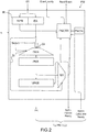
- FIG. 2 A block diagram of the packet maker is illustrated on figure 2 . Clock, enable and set/reset signals, as well as power supplies, are omitted for the sake of simplicity.
- Event-representing signals received from the FIFO buffer are temporarily stored in an input register IR.
- a controller PMCTR which may be modeled by a finite state machine, may read from register IR the population number NPN to perform a "filtering": only signals having particular values of the NPN fields are processed. The usefulness of this filtering operation will be explained later, with reference to figure 5 .
- the address field EA is provided to the select input SI of an M-output demultiplexer DMX, having a constant value of "1" applied to its data input DI.
- Each possible value of the address field EA i.e. each possible signal type, uniquely identifies an output of the demultiplexer, and a logical "1" is transferred to said output to be stored in a corresponding memory element of an M-bit register PKR. Before receiving the first signal, all the memory elements of said register had been initialized to "0".
- the address field of each incoming signal is also provided to the select input SI of an M-input multiplexer MX, whose output is connected to the controller PMCTR.
- MX M-input multiplexer
- PMCTR controller PMCTR
- the register PKR contains a fully formed" packet PK, which is transferred to another register, VPKR, in order to be provided to the packet maker output (in practice, this means that the matching unit receives a signal informing it that it can read the packet at the output of the packet maker, said output being directly connected to the register VPKR).
- VPKR Unlike PKR, whose content changes at each reception of an event-representing signal, VPKR always contains a "fully formed” signal, and its content only changes upon the completion of the next packet. This is why VPKR, and not PKR, is directly connected to the output of the packet maker.
- the controller exchanges different signals with other blocks of the circuit: it receives a "Event_ready” signal from the FIFO buffer, indicating that the buffer is not full, and sends to it a "Read Event” prompting the transmission of the first available signal to the input register IR; it sends a "Spike Packet Ready” signal to the match calculator unit MU and receives from it a "Match Calculator Ready”; the "Spike Packet Ready” signal also triggers the transfer of the packet PK from the register PKR to VPKR. And, depending on the received signals, it controls the operation of the other logical blocks (demultiplexer, multiplexer, counter, register).
- Figure 3 is a block diagram of the matching unit MU.
- the matching unit comprises a controller MCTRL - which, again, may be modeled by a finite state machine - controlling the operation of the logical blocks of the unit and exchanging signals with the controllers of other units. As discussed above, it exchanges "Spike Packet Ready” and "Match Calculator Ready” signals with the input unit in order to acquire packets PK from it. It also receives a "STDP Unit Ready” signal informing it when the learning unit is ready to update neurons.
- the main task of the packet maker is to calculate the matching between a packet PK and the binary weight vectors BWV of all the neurons - or at least of a predetermined subset thereof.
- the controller MCTRL increments a counter SYAC, whose content successively takes values corresponding to all the memory (or "synaptic") addresses SYA of the binary weights vector of the different neurons.
- the content of the counter is used to perform a reading access to the memory, allowing the matching unit to read the binary weight vector BWV and the learning threshold TL of the corresponding neuron, which are stored in respective registers.
- the current SYA address is also stored in a field of an output register OSR, connected to an output port of the circuit.
- Another field of the output register stores the population number NPN, which may be provided from a signal coming from outside the circuit, or be a constant value (e.g. if the filter implemented by the input unit controller ensures that only signals having a same population number are processed; in this case, the value of NPN stored in the output register OSR may be different from that of the processed signals; again, this issue will be discussed later with reference to figure 5 ).
- the synaptic address SYA is also stored in a field of another register, called the "learning event register" LER, to which the learning unit has access.
- the outputs of these logical gates are stored in an M-bit register MR, called the matching register.
- M-bit register MR M-bit register
- An adder MADD e.g. a three-stage pipelined adder
- the potential PT is provided at the input of three logical blocks:
- Digital comparers are well known digital elements.
- Logic block MIN can be obtained by combining a digital comparer and a multiplexer.
- Figures 4A and 4B form a block diagram of the learning unit LU.
- the learning unit receives a learning triggering signal LTS, comprising the learning event LEV and the LR flag, from the matching unit. More precisely, the LR signal triggers the storing of LEV in a FIFO buffer LUB. When it is full, and therefore unable to acquire further LTS signals, the buffer generates a "FIFO full” signal - whose complement constitutes the "STDP Unit Ready” transmitted to the controller MCTRL of the matching unit; when "STDP Unit Ready” goes to zero, the matching unit stops its operation, and when "STDP Unit Ready” goes again to one it resumes it.
- LTS learning triggering signal
- the buffer When empty, the buffer also generates a "FIFO empty” signal, which is transmitted to a controller LCTR of the learning unit; the "FIFO empty” signal is also transmitted to the controller MCTRL of the matching unit, which triggers the "Match Calculator Ready” flag when it is informed that the learning unit has finished its job.
- the controller can be modeled as a Finite State Machine, and supervises the operation of the logical blocks of the learning unit. In particular, it generates a "FIFO Read_en” signal triggering the extraction of the first available data element from the buffer LUB.
- the data element extracted from the buffer is a learning event LEV, which comprises a synaptic address SYA, i.e. the address of a neuron within the memory NM, and the updated learning threshold of the same neuron, TL'.
- SYA synaptic address
- TL' updated learning threshold of the same neuron
- Transmitting the synaptic address SYA to the memory NM triggers a reading operation of the data items, stored at said address, defining a neuron which has crossed the learning threshold.
- These data items are the binary weight vector BWV, the learning threshold TL itself and the swap number n swap . They are temporarily stored in an input register IOR.
- the learning threshold is not processed by the learning unit, so its storage could also be omitted. Instead, the learning unit changes the values of the binary weight vector BWV and, preferably, of the swap number n swap : this is the aim of the learning process.
- the updated values of the binary weight vector, BWV', and of the swap number, n' swap are stored in respective field of the output register LOR, together with TL' (see above).
- Updating n swap simply consists in subtracting the decrement dn swap from it, which is performed by a conventional subtracting block, SB1.
- Updating the binary weight vector is the most complex operation performed by the whole circuit. As explained above, it consists in swapping n swap "ones" and “zeros" within the vector. To ensure that the exact number of bits is swapped, the current (i.e. not updated) value of n swap , read from the IOR register, is transmitted to the controller LCTR, which stores it into a counter LUCN. The counter is decremented after each swapping operation; the learning process ends when its content reaches zero, and this triggers the generation of the "Write_enable" signal from the controller (see above).
- the bit swapping block WSLB which constitutes the bulk of the learning unit, receives at its inputs the data packet PK, generated from the packet maker PM, and the current binary weight vector BWV from the IOR register.
- the binary weight vector BWV and the complemented (i.e. passed through a bank of M “NOT” gates) data packet PK undergo a bit-wise logical AND operation, carried out by a bank of AND gates LAG1 operating in parallel.
- the result which is called the "ineffective weights vector" IWV is stored in a register.
- the IWV vector contains a "1" at each position corresponding to a "1" in the weight vector and a "0" in the data packet; otherwise stated, IWV represents active weights associated to missing events.
- the result which is called the "ineffective spikes vector” ISV is stored in a register.
- the ISV vector contains a "1" at each position corresponding to a "0" in the weight vector and a "1" in the data packet; otherwise stated, ISV represents events of the packet corresponding to inactive weights.
- the IWV and ISV vectors are transferred to respective circular shift registers CSR1, CSR2, and undergo a circular shift by a same (pseudo)random amount rv, determined by a random number generator RNG, controlled by the controller LCTR and having an output connected to a shift input port of each circular shift register.
- RNG random number generator
- the circularly-shifted vectors IWV and ISV then undergo a bit-wise logical AND operation with respective mask vectors WM, SM, stored by registers. Before the first swapping, all the bits of the mask vectors are set at a logical "1", therefore IWV and ISV are unchanged by the bit-wise AND operation.
- References WMAG, SMAG designate the banks of logical AND gates performing the operation.
- MIWV is a 1024-bit binary word
- figure 4C uses a 16-bit word for the sake of simplicity. More precisely, the value of IWV is taken to be "0010000010000000".
- This 16-bit word is used to fill a 4x4 two-dimensional array, whose lines are L0: "0010”; L1: “0000”; L2: “1000” and L3: "0000". Conversely, the columns are C0 "0010”; C1: "0000”; C2: “1000” and C3: "0000".
- the first active bit is the third one, i.e.
- OR gates POG1 - POG4 are used for OR-ing the bits of the four columns.
- the output of a logical gate is a bit taking the value "1" if the corresponding line contains at least one "1", representing an ineffective weight, and "0" otherwise.
- the bits corresponding to lines L0 and L2 are set to "1", those of lines L1 and L3 to "0".
- a first priority encoder PRE1 receives at its inputs the outputs of these logical gates (1 - 0 - 1 - 0). The inputs have different priorities: the one corresponding to line L0 has the highest priority, followed by L1, then L2 and finally L3.
- the output of the priority encoder is a 2-bit word identifying the highest-priority input having a "1" value; in this case, this output is "00", identifying line L0.
- This output is provided at the "select" input SI of a multiplexer PMUX, whose four inputs are connected to respective lines of the columns. Therefore, the four bits of the selected line L0 are present on the output of the multiplexer, to be provided as inputs to a second priority encoder PRE2, whose output is another 2-bit word identifying the position of the first "1" of the line - in this case "10", corresponding to the third position.
- a 4-bit number is then formed by juxtaposing the outputs of the first and second priority encoders, in this order. The value of this number (“0010", i.e. 2) corresponds to the position of the first "1" within the IWV vector - i.e. the third position.
- the random number rv determining the amount of the circular shift is then subtracted from the output of logical blocks FFAB1, FFAB2 using subtracting blocks SB2, SB3. It is important to note that these are "circular" subtractions: for instance, if the output of FFAB1, that of FFAB2 and rv are 10-bit binary words, a negative result -
- -1; therefore, the result will always be comprised between 0 and 2 10 -1 1023.
- the results of the subtractions represent the rv th active bits of the IWV and of the ISV vectors. Otherwise stated, the subtractions readjust the positions found by logical blocks FFAB1, FFAB2, compensating the circular shift.
- a first multiplexer LMUX1 has two data inputs connected to the outputs of the subtracting blocks SB2, SB3, a select input SI connected to the controller LCTR and an output connected to an address input of a register UWR, whose content has been initialized to the current value of the weight vector BWV.
- a second multiplexer LMUX2 has two data inputs receiving constant binary values: "1" and "0", a select input SI connected to the controller LCTR and an output connected to a data input of register UWR.
- the register also has a "write_enable” input receiving a signal (reference wr_en) generated by the controller.
- the multiplexer can be used to write a "0" at the position of the rv th ineffective weight of the binary weight vector, and a "1" at the position of the rv th ineffective spike. This is the first of the required swapping operations, improving the match between the weight vector and the data packet.
- the output of SB2 is also applied to an address input of the register storing the WM mask, said register having a constant "0" applied at its data input.
- the output of SB3 is also applied to an address input of the register storing the SM mask, said register having a constant "0” applied at its data input.
- the updated masks are then bit-wise AND-ed with the circularly shifted IWV and ISV vectors, the results being applied at the input of logical blocks FFAB1, FFAB2. Due to the bit-wise AND operations with the updated mask, the first active bits of IWV and ISV are now put to zero, therefore FFAB1 and FFAB2 find the second active bits of the original IWV/ISV vectors, and so on.
- the updated binary weight vector BWV' contained in the UWR register, is then transmitted to the corresponding field of the output vector LOR, before being written into the memory, as already explained.
- the circuit described above has been implemented using a XC6SLX150T-3 Spartan-6 ® FPGA by Xilinx ®. Synthesis was performed using Verilog language and a XST synthesizer, also by Xilinx.
- the initial value of the learning threshold was taken to be 7, and its final value (TL MAX ) was 12; the firing threshold was also equal to 12.
- n swap was 32, with a decrement dn swap of 8 down to 0 (or, in some other embodiment, to a nonzero minimal value, e.g. 1).
- all these parameters are programmable in the FPGA through a JTAG port.
- a set of 64 "conventional" supervised STDP neurons was added to classify the detected pattern.
- a supervised STDP neuron has an extra external input (called “supervisor”), encoded also through AER (Address Event Representation), which forces post-synaptic spikes from this neuron when its representative "category” (or feature) is present at the input. Therefore, whenever a "supervisor” spike arrives, the corresponding active synapses will be potentiated. Otherwise active synapses will be depressed.
- Suitable STDP neurons are described e.g. in the paper by Masquelier T, Guyonneau R, and Thorpe SJ "Spike Timing Dependent Plasticity Finds the Start of Repeating Patterns in Continuous Spike Trains" PLoS ONE 3(1): e1377 (2008 ).
- the circuit was operated at a clock frequency of 100 MHz.
- the learning unit was able to accept about one packet every 10.24 ⁇ s, i.e. every 1024 clock cycle.
- Each packet contained 64 events (spikes), therefore the theoretical event acceptance rate of the circuit was of about 6 Meps (million events per seconds); in practice, an acceptance rate of 5.3 Meps was actually achieved.
- a software simulation running on one core of an Intel ® CoreTM i5 CPU could not exceed 10 keps (thousand events per second).
- Power consumption at maximum speed rate was 530 mW: 143 mW of static consumption and 387 mW of dynamic consumption, corresponding to 73 nJ for each input spike. It has been estimated that a standard-cell ASIC implementation, based for instance on Toshiba's FFSATM technology) would reduce consumption by 70% while improving speed by a factor of 5.
- the circuit has been tested using event-representing signals generated by a simulator. Repeating patterns were generated, including at least one event among 32 different event types; signals representing 992 other event types were generated randomly. It was found that 6 presentations were sufficient to ensure reliable detection of the patterns.
- the detection algorithm turned out to be quite insensitive to spike loss: the rate of successful detection was only reduced by 2% (from 100% to 98%) if 40% of the spikes were deleted; the rate was still of 88% with a 50% deletion rate. It also proved reasonably insensitive to jitter: at an input spike rate of 20.48 keps (average time to make a packet: about 3.2 ms) a jitter of up to 2 ms only reduced the detection rate by 4% (from 100% to 96%).
- Figure 5 illustrates a diagram of a digital system comprising a plurality of digital electronic circuits of the type described above - in the figure there are three such circuits: SNN1, SNN2 and SNN3. Each of these circuits implements a population filter: PF1, PF2, PF3, only allowing in event-representing signals characterized by a particular population number.
- the filters are represented as separate logic blocks but, as explained above, they may be implemented by the input unit controllers.
- an additional circuit SUP implementing a different, supervised, artificial neural network (of any known type) may also be present.
- circuits SNN1, SNN2, SNN3 and SUP are connected to respective input ports of a digital signal merger SMG, having a single output which is connected to the inputs of the circuits, thus implementing a data loop.
- An event generator EG for instance, a dynamic vision sensor, or DVS
- IIC for instance, an Address-Event-Representation - AER - interface
- An output interface circuit OIC for instance, another AER interface
- the merger SMG provides arbitration to manage the collisions between output signals of circuits "firing" almost simultaneously.
- the input interface generates event-representing signals ES with a population number of 1; therefore they are processed by circuits SNN1 and SNN2. These circuits have a matching unit configured to generate output signals having a population number of 2; this way, these output signals constitute events suitable to be processed by circuit SNN3. In turn, this circuit produces output signals with population number of 3, suitable to be processed by the supervised artificial neural network SUP. And the output signals of this latter circuit have a population number of 4, in order to be accepted by the output interface.
- the system implements a multi-layer neural network wherein circuits SNN1 and SNN2 implement a first layer, circuit SNN3 a second layer and SUP a third layer. The first and second layers perform unsupervised detection of recurring pattern, while the third (supervised) layer associates each detected pattern to a predetermined class.
- a general controller GCTR supervises the operation of the system. For instance, it may set the values of different parameters of the circuits of the systems (e.g. TL, TF, n swap , N, the population numbers of the filters...; in figures 2 - 4 , all these parameters are represented by signal coming from outside the units), perform different tests etc.
- TL, TF, n swap , N the population numbers of the filters...; in figures 2 - 4 , all these parameters are represented by signal coming from outside the units
- the system of figure 5 may be implemented in a single FPGA (or another kind of programmable device), or ASIC, or in the form of a multi-chip system.
- the implementation of one or some logic blocks may be changed without changing that of the other blocks - except, if necessary, for ensuring the compatibility of the data formats.
- the disclosed implementations are believed to realize an optimal trade-off between complexity, speed and power consumption.
- n swap random numbers could be generated successively in order to swap non-successive ineffective weight and ineffective spike bits. This implementation, however, would be much slower.
- the data representations may also be changed to a certain extent.
- the binary weight vector of each neuron is represented by a single M-bit binary word.
- This implementation is less flexible and a conversion to the "explicit" M-bit representation is required in order to be able to perform the bitwise AND operation in the matching unit and in the learning unit.
- the number W of weights is not necessarily the same for all the neurons; similarly, thresholds TL and TF may be different from a neuron to another. If different neuron uses different values for TF, the matching unit will have to be slightly modified in order to include an additional register storing the TF value for the currently processed neuron.
Landscapes
- Engineering & Computer Science (AREA)
- Theoretical Computer Science (AREA)
- Physics & Mathematics (AREA)
- Data Mining & Analysis (AREA)
- Life Sciences & Earth Sciences (AREA)
- General Physics & Mathematics (AREA)
- Evolutionary Computation (AREA)
- Artificial Intelligence (AREA)
- General Engineering & Computer Science (AREA)
- Biophysics (AREA)
- Biomedical Technology (AREA)
- Health & Medical Sciences (AREA)
- Computational Linguistics (AREA)
- Software Systems (AREA)
- Computing Systems (AREA)
- Mathematical Physics (AREA)
- Molecular Biology (AREA)
- General Health & Medical Sciences (AREA)
- Bioinformatics & Cheminformatics (AREA)
- Bioinformatics & Computational Biology (AREA)
- Computer Vision & Pattern Recognition (AREA)
- Evolutionary Biology (AREA)
- Neurology (AREA)
- Multimedia (AREA)
- Image Analysis (AREA)
Claims (13)
- Digitale elektronische Schaltung (SNN), die ein gepulstes neuronales Netzwerke implementiert und Folgendes umfasst:- eine Eingangseinheit (IU), konfiguriert zum Empfangen, an einem Eingangsport der digitalen elektronischen Schaltung, einer Reihe von digitalen Signalen (ES), die jeweilige Ereignisse darstellen, wobei jedes Signal der Reihe zu einem Signaltyp eines M-Element-Satzes von Signaltypen gehört, und zum Erzeugen eines Datenpakets (PK), das für N zusammenhängende Signale der Reihe repräsentativ ist, wobei 1<N<M ist;- einen Speicher (NM) zum Speichern von einer Mehrzahl von Neuronen definierenden Daten, wobei die jedes der Neuronen definierenden Daten einen Satz von binären Gewichtungen (BWV) umfassen, die für einen Teilsatz des Satzes von Signaltypen repräsentativ sind;- eine Übereinstimmungsberechnungseinheit (MCU), die mit der Eingangseinheit und dem Speicher verbunden ist, konfiguriert zum:
Empfangen eines Datenpakets (PK) von der Eingangseinheit; zum Berechnen, für mindestens einige der durch die vom Speicher (NM) gespeicherten Daten definierten Neuronen, eines Potentialwertes (PT), der für die Anzahl von Signalen des Eingangspakets repräsentativ ist, deren Typen zum Teilsatz des Neurons gehören; und zum Erzeugen, an einem Ausgangsport der digitalen elektronischen Schaltung, einer Reihe von Ausgangssignalen (OS), die Neuronen mit einem Potentialwert anzeigen, der einen Schwellenwert TF, Feuerungsschwelle genannt, überschreitet; und- eine Lerneinheit (LU), die mit der Eingangseinheit, der Übereinstimmungsberechnungseinheit und dem Speicher verbunden ist, die zum Modifizieren, innerhalb des Speichers, des Satzes von binären Gewichtungen von Neuronen mit einem Potentialwert konfiguriert sind, der einen Schwellenwert TL, Lernschwelle genannt, überschreitet, wobei das Modifizieren das Vertauschen von nswap≥1 binären Gewichtungen, die für Signaltypen des Teilsatzes des Satzes von nicht im Eingangspaket enthaltenen Signaltypen repräsentativ sind, mit der gleichen Anzahl von binären Gewichtungen umfasst, die für Signaltypen repräsentativ sind, die im Eingangspaket enthalten sind und derzeit nicht zum Teilsatz des Satzes von Signaltypen gehören; wobei:- der Satz von binären Gewichtungen (BWV) jedes Neurons, der für den Teilsatz des Satzes von Signaltypen repräsentativ ist, durch einen vom Speicher gespeicherten booleschen Vektor implementiert wird, wobei der Vektor M Komponenten aufweist, wobei jede Komponente mit einem anderen Signaltyp des M-Element-Satzes von Signaltypen assoziiert ist, wobei die mit den Elementen des Teilsatzes assoziierten Komponenten einen ersten booleschen Wert annehmen und die übrigen Komponenten einen zweiten booleschen Wert annehmen, der sich von dem ersten unterscheidet:- die Eingangseinheit einen Demultiplexer (DMX) mit einem Dateneingang (DI), einem Auswahleingang (SI) und M Ausgängen und ein M-Bit-Register (PKR) mit M Speicherelementen umfasst, von denen jedes einen mit einem jeweiligen Ausgang des Demultiplexers verbundenen Dateneingang aufweist, wobei der Demultiplexer zum Empfangen eines ersten konstanten Binärwertes an seinem Dateneingang und eines digitalen Signals (ES) oder eines Teils eines digitalen Signals (EA) an seinem Auswahleingang konfiguriert ist, das zu einem Signaltyp des M-Element-Satzes von Signaltypen gehört, wodurch ein erster konstanter boolescher Wert in einem der mit dem Signaltyp assoziierten M Speicherelemente gespeichert wird, wobei die M Speicherelemente des Registers mit einem zweiten konstanten booleschen Wert initialisiert werden, der sich von dem ersten unterscheidet; und- die Lerneinheit Folgendes umfasst:- eine erste Bank von logischen UND-Gattern (LAG1), konfiguriert zum Empfangen, an ihren Eingängen, des Satzes von binären Gewichtungen (BWV) für ein Neuron und einer invertierten Version eines von der Eingangseinheit erzeugten Datenpakets, wobei die Ausgangssignale der ersten Bank von logischen UND-Gattern ein erstes binäres Wort (IWV) bilden, Ineffektive-Gewichtungen-Vektor genannt;- eine zweite Bank von logischen UND-Gattern (LAG2), konfiguriert zum Empfangen, an ihren Eingängen, einer invertierten Version des Satzes von binären Gewichtungen (BWV) und des Datenpakets (PK), wobei die Ausgangssignale der ersten Bank von logischen UND-Gattern ein zweites binäres Wort (ISV) bilden, Ineffektive-Pulse-Vektor genannt;- ein erstes (CSR1) und zweites (CSR2) Ringschieberegister zum Speichern des Ineffektive-Gewichtungen-Vektors und des Ineffektive-Pulse-Vektors;- einen Zufallszahlengenerator (RNG), der mit dem ersten und zweiten Ringschieberegister verbunden ist, um zu bewirken, dass der Inhalt der Register eine Ringverschiebung um denselben zufälligen Betrag (rv) erfährt; und- einen logischen Block (WSLB), konfiguriert zum:- Bestimmen der Positionen der nswaps ersten Bits des Inhalts des ersten Ringschieberegisters mit einem ersten Binärwert, dann Nachjustieren der bestimmten Position zum Kompensieren des zufälligen Betrags (rv) der Ringverschiebung;- Bestimmen der Positionen der nswaps ersten Bits des Inhalts des zweiten Ringschieberegisters mit dem ersten Binärwert, dann Nachjustieren der bestimmten Position zum Kompensieren des zufälligen Betrags (rv) der Ringverschiebung;- Speichern eines zweiten Binärwerts, der sich vom ersten Binärwert unterscheidet, in einem Speicherelement eines temporären Registers (UWR), das innerhalb des Registers die ersten nachjustierten Positionen aufweist; Speichern des ersten Binärwerts in den Speicherelementen des temporären Registers, die innerhalb des Registers die zweiten nachjustierten Positionen aufweisen; und Halten des Inhalts der übrigen Speicherelemente des temporären Registers unverändert;wobei die Lerneinheit ferner zum Zuführen des Inhalts des temporären Registers dem Speicher als den aktualisierten Satz von binären Gewichtungen (BWV') für das entsprechende Neuron konfiguriert ist. - Digitale elektronische Schaltung nach Anspruch 1, wobei die vom Speicher gespeicherten und jedes Neuron definierenden Daten auch Werte von TL und nswap umfassen.
- Digitale elektronische Schaltung nach Anspruch 2, wobei mindestens eine aus der Übereinstimmungseinheit und der Lerneinheit ferner zum Modifizieren der vom Speicher gespeicherten Werte von TL und nswap durch Verringern von TL und Erhöhen von nswap mit zunehmendem Potentialwert des entsprechenden Neurons konfiguriert ist.
- Digitale elektronische Schaltung nach einem der vorherigen Ansprüche, wobei die vom Speicher gespeicherten und jedes Neuron definierenden Daten auch einen Wert von TF umfassen.
- Digitale elektronische Schaltung nach einem der vorherigen Ansprüche, wobei die Teilsätze des Satzes von mit allen Neuronen assoziierten Signaltypen eine gleiche Anzahl W<N von Elementen haben.
- Digitale elektronische Schaltung nach einem der vorherigen Ansprüche, die ferner einen Zähler (PMCN) und einen Controller (PMCTR) umfasst, wobei der Controller konfiguriert ist zum:
Vergleichen des Inhalts des M-Bit-Registers (PKR) mit dem an seinem Auswahleingang anliegenden digitalen Signal, um den Inhalt des mit dem Signaltyp assoziierten Speicherelements zu bestimmen, zu dem das digitale Signal (ES) gehört; zum Inkrementieren des Zählers, wenn der Inhalt den zweiten konstanten booleschen Wert hat, und zum Zuführen des Inhalts des M-Bit-Registers, der das Datenpaket (PK) bildet, zur Übereinstimmungsberechnungseinheit, wenn der Zähler anzeigt, dass zu N verschiedenen Signaltypen gehörende Digitalsignale empfangen wurden. - Digitale elektronische Schaltung nach einem der vorherigen Ansprüche, wobei die Übereinstimmungsberechnungseinheit eine Bank von logischen UND-Gattern (MAG), einen Binäraddierer (MADD), einen ersten (MCMP1) digitalen Komparator und einen Controller (MCTRL) umfasst, wobei der Controller konfiguriert ist zum:- sukzessiven Auslesen der Sätze von binären Gewichten (BWV) einer Mehrzahl von den Neuronen aus dem Speicher;- Verwenden der Bank von logischen UND-Gattern (MAG) zum Berechnen von M-Bit übereinstimmenden Binärwörtern durch Ausführen einer bitweisen logischen UND-Operation zwischen jedem der Sätze von binären Gewichtungen und dem von der Eingangseinheit empfangenen Datenpaket;- Verwenden des Binäraddierers (MADD) zum Berechnen von Neuronenpotentialen (PT) durch Addieren der Bits jedes übereinstimmenden Binärwortes; und- Verwenden des ersten digitalen Komparators (MCMP1) zum Durchführen eines Vergleichs jedes Neuronenpotentials mit dem Feuerungsschwellenwert TF und, abhängig vom Ergebnis des Vergleichs, zum Erzeugen des Ausgangssignals (OS).
- Digitale elektronische Schaltung nach Anspruch 7, wobei die Übereinstimmungsberechnungseinheit ferner einen zweiten digitalen Komparator (MCMP2) umfasst, und ihr Controller (MCTRL) ferner konfiguriert ist zum:- Verwenden des zweiten digitalen Komparators (MCMP2) zum Durchführen eines Vergleichs jedes Neuronenpotentials mit der Lernschwelle TL und, abhängig vom Ergebnis des Vergleichs, zum Erzeugen eines Lernauslösesignals (LTS), das das Neuron anzeigt, und Übertragen desselben zu der Lerneinheit.
- Digitale elektronische Schaltung nach einem der Ansprüche 7 und 8, wobei die Übereinstimmungsberechnungseinheit auch einen digitalen Block (MIN) zum Auswählen des kleinsten aus dem Potentialwert und einem Endwert der Lernschwelle und zum Zuführen desselben zum Speicher als neuen Wert (TL') von TL für das entsprechende Neuron umfasst.
- Digitale elektronische Schaltung nach einem der vorherigen Ansprüche, wobei jedes digitale Signal der Reihe (ES) auch einen Indikator einer Neuronenpopulation (NPN) umfasst und wobei die Eingangseinheit auch ein Filter (PF1 - PF3) umfasst, das zum Zulassen oder Zurückweisen eingehender digitaler Signale in Abhängigkeit von einem Wert des entsprechenden Indikators einer Neuronenpopulation konfiguriert ist.
- Digitales elektronisches System, das Folgendes umfasst:- eine Mehrzahl von digitalen elektronischen Schaltungen (SNN1 bis SNN3) nach Anspruch 10, von denen mindestens zwei Eingangseinheiten mit Filtern (PF1 bis PF3) umfassen, konfiguriert zum Zulassen eingehender digitaler Signale mit unterschiedlichen Werten des Indikators einer Neuronenpopulation (NPN), wobei die Übereinstimmungseinheiten der digitalen elektronischen Schaltung zum Erzeugen eines Ausgangssignals konfiguriert sind, das auch einen aktualisierten Indikator einer Neuronenpopulation enthält; und. einen Signalzusammenführer (SMG) mit einer Mehrzahl von Eingangsports und einem einzigen Ausgangsport, wobei die Eingangsports des Signalzusammenführers mit den Ausgangsports der digitalen elektronischen Schaltungen verbunden sind und der Ausgangsport des Signalzusammenführers mit den Eingangsports der digitalen elektronischen Schaltungen und mit einem Ausgangsport des digitalen elektronischen Systems verbunden ist.
- Digitales elektronisches System nach Anspruch 11, das ferner eine digitale Schaltung umfasst, die ein überwachtes künstliches neuronales Netzwerk (SUP) mit einem Eingangsport und einem Ausgangsport implementiert, wobei der Eingangsport der Schaltung mit dem Ausgangsport des Signalzusammenführers über ein Filter (PF4) verbunden ist, das zum Zulassen oder Zurückweisen eingehender digitaler Signale in Abhängigkeit von einem Wert des entsprechenden Indikators einer Neuronenpopulation konfiguriert ist, wobei der Ausgangsport der Schaltung mit einem Eingangsport des Signalzusammenführers verbunden ist.
- Digitale(s) elektronische(s) Schaltung oder System nach einem der vorherigen Ansprüche, implementiert durch ein FPGA.
Priority Applications (3)
| Application Number | Priority Date | Filing Date | Title |
|---|---|---|---|
| US16/349,248 US11853862B2 (en) | 2016-11-21 | 2017-11-20 | Method, digital electronic circuit and system for unsupervised detection of repeating patterns in a series of events |
| PCT/EP2017/079767 WO2018091706A1 (en) | 2016-11-21 | 2017-11-20 | Method, digital electronic circuit and system for unsupervised detection of repeating patterns in a series of events |
| US16/417,218 US20190340494A1 (en) | 2016-11-21 | 2019-05-20 | Method, Digital Electronic Circuit and System for Unsupervised Detection of Repeating Patterns in a Series of Events |
Applications Claiming Priority (1)
| Application Number | Priority Date | Filing Date | Title |
|---|---|---|---|
| EP16306525.3A EP3324343A1 (de) | 2016-11-21 | 2016-11-21 | Unüberwachte detektion von sich wiederholenden mustern in eine reihe von ereignissen |
Publications (2)
| Publication Number | Publication Date |
|---|---|
| EP3324344A1 EP3324344A1 (de) | 2018-05-23 |
| EP3324344B1 true EP3324344B1 (de) | 2021-06-30 |
Family
ID=58098388
Family Applications (2)
| Application Number | Title | Priority Date | Filing Date |
|---|---|---|---|
| EP16306525.3A Ceased EP3324343A1 (de) | 2016-11-21 | 2016-11-21 | Unüberwachte detektion von sich wiederholenden mustern in eine reihe von ereignissen |
| EP17305186.3A Active EP3324344B1 (de) | 2016-11-21 | 2017-02-20 | Digitale elektronische schaltung und system zum implementieren eines gepulsten neuronalen netzes zur durchführung von unüberwachten nachweisen von mustern |
Family Applications Before (1)
| Application Number | Title | Priority Date | Filing Date |
|---|---|---|---|
| EP16306525.3A Ceased EP3324343A1 (de) | 2016-11-21 | 2016-11-21 | Unüberwachte detektion von sich wiederholenden mustern in eine reihe von ereignissen |
Country Status (3)
| Country | Link |
|---|---|
| US (2) | US11853862B2 (de) |
| EP (2) | EP3324343A1 (de) |
| WO (1) | WO2018091706A1 (de) |
Families Citing this family (10)
| Publication number | Priority date | Publication date | Assignee | Title |
|---|---|---|---|---|
| US11301753B2 (en) * | 2017-11-06 | 2022-04-12 | Samsung Electronics Co., Ltd. | Neuron circuit, system, and method with synapse weight learning |
| US20210166106A1 (en) * | 2017-12-12 | 2021-06-03 | The Regents Of The University Of California | Residual binary neural network |
| TWI700647B (zh) * | 2018-09-11 | 2020-08-01 | 國立清華大學 | 電子裝置及類神經網路的壓縮方法 |
| US11468299B2 (en) | 2018-11-01 | 2022-10-11 | Brainchip, Inc. | Spiking neural network |
| EP3881241A1 (de) * | 2018-11-18 | 2021-09-22 | Innatera Nanosystems B.V. | Neuronales spiking-netz |
| JP6852141B2 (ja) * | 2018-11-29 | 2021-03-31 | キヤノン株式会社 | 情報処理装置、撮像装置、情報処理装置の制御方法、および、プログラム |
| CN118468107A (zh) | 2019-07-25 | 2024-08-09 | 智力芯片有限责任公司 | 数字尖峰卷积神经网络系统和执行卷积的计算机实施方法 |
| US12614061B2 (en) * | 2020-08-27 | 2026-04-28 | Micron Technology, Inc. | Pipelining spikes during memory access in spiking neural networks |
| US11494627B1 (en) | 2021-07-08 | 2022-11-08 | Hong Kong Applied Science and Technology Research Institute Company Limited | Dynamic tile parallel neural network accelerator |
| US11687479B2 (en) | 2021-09-23 | 2023-06-27 | International Business Machines Corporation | System event broadcast synchronization across hierarchical interfaces |
Family Cites Families (10)
| Publication number | Priority date | Publication date | Assignee | Title |
|---|---|---|---|---|
| US9129220B2 (en) | 2010-07-07 | 2015-09-08 | Qualcomm Incorporated | Methods and systems for digital neural processing with discrete-level synapes and probabilistic STDP |
| US9047568B1 (en) * | 2012-09-20 | 2015-06-02 | Brain Corporation | Apparatus and methods for encoding of sensory data using artificial spiking neurons |
| US9111222B2 (en) * | 2011-11-09 | 2015-08-18 | Qualcomm Incorporated | Method and apparatus for switching the binary state of a location in memory in a probabilistic manner to store synaptic weights of a neural network |
| US9367797B2 (en) | 2012-02-08 | 2016-06-14 | Jason Frank Hunzinger | Methods and apparatus for spiking neural computation |
| US9563841B2 (en) | 2012-07-31 | 2017-02-07 | International Business Machines Corporation | Globally asynchronous and locally synchronous (GALS) neuromorphic network |
| US20140143193A1 (en) | 2012-11-20 | 2014-05-22 | Qualcomm Incorporated | Method and apparatus for designing emergent multi-layer spiking networks |
| US9195934B1 (en) | 2013-01-31 | 2015-11-24 | Brain Corporation | Spiking neuron classifier apparatus and methods using conditionally independent subsets |
| US10489700B1 (en) * | 2014-07-07 | 2019-11-26 | Crossbar, Inc. | Neuromorphic logic for an array of high on/off ratio non-volatile memory cells |
| US9886662B2 (en) | 2014-09-19 | 2018-02-06 | International Business Machines Corporation | Converting spike event data to digital numeric data |
| US20160358069A1 (en) | 2015-06-03 | 2016-12-08 | Samsung Electronics Co., Ltd. | Neural network suppression |
-
2016
- 2016-11-21 EP EP16306525.3A patent/EP3324343A1/de not_active Ceased
-
2017
- 2017-02-20 EP EP17305186.3A patent/EP3324344B1/de active Active
- 2017-11-20 WO PCT/EP2017/079767 patent/WO2018091706A1/en not_active Ceased
- 2017-11-20 US US16/349,248 patent/US11853862B2/en active Active
-
2019
- 2019-05-20 US US16/417,218 patent/US20190340494A1/en not_active Abandoned
Non-Patent Citations (4)
| Title |
|---|
| HOOMAN JAROLLAHI ET AL: "Architecture and implementation of an associative memory using sparse clustered networks", 2012 IEEE INTERNATIONAL SYMPOSIUM ON CIRCUITS AND SYSTEMS, 20 May 2012 (2012-05-20), pages 2901 - 2904, XP055061304, ISBN: 978-1-46-730217-3, DOI: 10.1109/ISCAS.2012.6271922 * |
| PHILIPPE COUSSY ET AL: "Fully Binary Neural Network Model and Optimized Hardware Architectures for Associative Memories", ACM JOURNAL ON EMERGING TECHNOLOGIES IN COMPUTING SYSTEMS (JETC), ACM, 2 PENN PLAZA, SUITE 701 NEW YORK NY 10121-0701 USA, vol. 11, no. 4, 27 April 2015 (2015-04-27), pages 1 - 23, XP058067821, ISSN: 1550-4832, DOI: 10.1145/2629510 * |
| RASTEGARI MOHAMMAD ET AL: "XNOR-Net: ImageNet Classification Using Binary Convolutional Neural Networks", INTERNATIONAL CONFERENCE ON FINANCIAL CRYPTOGRAPHY AND DATA SECURITY; [LECTURE NOTES IN COMPUTER SCIENCE; LECT.NOTES COMPUTER], SPRINGER, BERLIN, HEIDELBERG, vol. 9908 Chap.32, no. 558, 17 September 2016 (2016-09-17), pages 525 - 542, XP047355418, ISBN: 978-3-642-17318-9, [retrieved on 20160917] * |
| STEVEN K. ESSER ET AL: "Convolutional networks for fast, energy-efficient neuromorphic computing", PROCEEDINGS OF THE NATIONAL ACADEMY OF SCIENCES, vol. 113, no. 41, 11 October 2016 (2016-10-11), pages 11441 - 11446, XP055704757, ISSN: 0027-8424, DOI: 10.1073/pnas.1604850113 * |
Also Published As
| Publication number | Publication date |
|---|---|
| US20190286944A1 (en) | 2019-09-19 |
| EP3324344A1 (de) | 2018-05-23 |
| US11853862B2 (en) | 2023-12-26 |
| US20190340494A1 (en) | 2019-11-07 |
| WO2018091706A1 (en) | 2018-05-24 |
| EP3324343A1 (de) | 2018-05-23 |
Similar Documents
| Publication | Publication Date | Title |
|---|---|---|
| EP3324344A1 (de) | Digitale elektronische schaltung und system zum implementieren eines gepulsten neuronalen netzes zur durchführung von unüberwachten nachweisen von mustern | |
| KR102788329B1 (ko) | 개선된 스파이킹 뉴럴 네트워크 | |
| KR102592146B1 (ko) | 시냅스 가중치 학습을 위한 뉴런 회로, 시스템 및 방법 | |
| US11238343B2 (en) | Scalable neural hardware for the noisy-OR model of Bayesian networks | |
| KR102588838B1 (ko) | 초전도 뉴로모픽 코어 | |
| TWI515670B (zh) | 用以強化學習之裝置、系統及電腦程式產品 | |
| US8812414B2 (en) | Low-power event-driven neural computing architecture in neural networks | |
| US9239984B2 (en) | Time-division multiplexed neurosynaptic module with implicit memory addressing for implementing a neural network | |
| US20140180984A1 (en) | Time-division multiplexed neurosynaptic module with implicit memory addressing for implementing a universal substrate of adaptation | |
| US10755166B2 (en) | Transform architecture for multiple neurosynaptic core circuits | |
| US10832121B2 (en) | Transform for a neurosynaptic core circuit | |
| Babu et al. | Stochastic deep learning in memristive networks | |
| Feng et al. | Impact of geometrical structures on the output of neuronal models: a theoretical and numerical analysis | |
| Kornijcuk et al. | Pointer based routing scheme for on-chip learning in neuromorphic systems | |
| Sundstrom et al. | ATM data classification with an artificial neural network |
Legal Events
| Date | Code | Title | Description |
|---|---|---|---|
| PUAI | Public reference made under article 153(3) epc to a published international application that has entered the european phase |
Free format text: ORIGINAL CODE: 0009012 |
|
| STAA | Information on the status of an ep patent application or granted ep patent |
Free format text: STATUS: THE APPLICATION HAS BEEN PUBLISHED |
|
| AK | Designated contracting states |
Kind code of ref document: A1 Designated state(s): AL AT BE BG CH CY CZ DE DK EE ES FI FR GB GR HR HU IE IS IT LI LT LU LV MC MK MT NL NO PL PT RO RS SE SI SK SM TR |
|
| AX | Request for extension of the european patent |
Extension state: BA ME |
|
| STAA | Information on the status of an ep patent application or granted ep patent |
Free format text: STATUS: REQUEST FOR EXAMINATION WAS MADE |
|
| 17P | Request for examination filed |
Effective date: 20181115 |
|
| RBV | Designated contracting states (corrected) |
Designated state(s): AL AT BE BG CH CY CZ DE DK EE ES FI FR GB GR HR HU IE IS IT LI LT LU LV MC MK MT NL NO PL PT RO RS SE SI SK SM TR |
|
| STAA | Information on the status of an ep patent application or granted ep patent |
Free format text: STATUS: EXAMINATION IS IN PROGRESS |
|
| 17Q | First examination report despatched |
Effective date: 20190322 |
|
| GRAP | Despatch of communication of intention to grant a patent |
Free format text: ORIGINAL CODE: EPIDOSNIGR1 |
|
| STAA | Information on the status of an ep patent application or granted ep patent |
Free format text: STATUS: GRANT OF PATENT IS INTENDED |
|
| INTG | Intention to grant announced |
Effective date: 20210129 |
|
| RAP1 | Party data changed (applicant data changed or rights of an application transferred) |
Owner name: CONSEJO SUPERIOR DE INVESTIGACIONES CIENTIFICAS (CSIC) Owner name: CENTRE NATIONAL DE LA RECHERCHE SCIENTIFIQUE |
|
| GRAS | Grant fee paid |
Free format text: ORIGINAL CODE: EPIDOSNIGR3 |
|
| GRAA | (expected) grant |
Free format text: ORIGINAL CODE: 0009210 |
|
| STAA | Information on the status of an ep patent application or granted ep patent |
Free format text: STATUS: THE PATENT HAS BEEN GRANTED |
|
| AK | Designated contracting states |
Kind code of ref document: B1 Designated state(s): AL AT BE BG CH CY CZ DE DK EE ES FI FR GB GR HR HU IE IS IT LI LT LU LV MC MK MT NL NO PL PT RO RS SE SI SK SM TR |
|
| REG | Reference to a national code |
Ref country code: CH Ref legal event code: EP |
|
| REG | Reference to a national code |
Ref country code: AT Ref legal event code: REF Ref document number: 1407023 Country of ref document: AT Kind code of ref document: T Effective date: 20210715 |
|
| REG | Reference to a national code |
Ref country code: DE Ref legal event code: R096 Ref document number: 602017041157 Country of ref document: DE |
|
| REG | Reference to a national code |
Ref country code: IE Ref legal event code: FG4D |
|
| REG | Reference to a national code |
Ref country code: LT Ref legal event code: MG9D |
|
| PG25 | Lapsed in a contracting state [announced via postgrant information from national office to epo] |
Ref country code: FI Free format text: LAPSE BECAUSE OF FAILURE TO SUBMIT A TRANSLATION OF THE DESCRIPTION OR TO PAY THE FEE WITHIN THE PRESCRIBED TIME-LIMIT Effective date: 20210630 Ref country code: HR Free format text: LAPSE BECAUSE OF FAILURE TO SUBMIT A TRANSLATION OF THE DESCRIPTION OR TO PAY THE FEE WITHIN THE PRESCRIBED TIME-LIMIT Effective date: 20210630 Ref country code: BG Free format text: LAPSE BECAUSE OF FAILURE TO SUBMIT A TRANSLATION OF THE DESCRIPTION OR TO PAY THE FEE WITHIN THE PRESCRIBED TIME-LIMIT Effective date: 20210930 |
|
| REG | Reference to a national code |
Ref country code: NL Ref legal event code: MP Effective date: 20210630 |
|
| REG | Reference to a national code |
Ref country code: AT Ref legal event code: MK05 Ref document number: 1407023 Country of ref document: AT Kind code of ref document: T Effective date: 20210630 |
|
| PG25 | Lapsed in a contracting state [announced via postgrant information from national office to epo] |
Ref country code: LV Free format text: LAPSE BECAUSE OF FAILURE TO SUBMIT A TRANSLATION OF THE DESCRIPTION OR TO PAY THE FEE WITHIN THE PRESCRIBED TIME-LIMIT Effective date: 20210630 Ref country code: GR Free format text: LAPSE BECAUSE OF FAILURE TO SUBMIT A TRANSLATION OF THE DESCRIPTION OR TO PAY THE FEE WITHIN THE PRESCRIBED TIME-LIMIT Effective date: 20211001 Ref country code: NO Free format text: LAPSE BECAUSE OF FAILURE TO SUBMIT A TRANSLATION OF THE DESCRIPTION OR TO PAY THE FEE WITHIN THE PRESCRIBED TIME-LIMIT Effective date: 20210930 Ref country code: SE Free format text: LAPSE BECAUSE OF FAILURE TO SUBMIT A TRANSLATION OF THE DESCRIPTION OR TO PAY THE FEE WITHIN THE PRESCRIBED TIME-LIMIT Effective date: 20210630 Ref country code: RS Free format text: LAPSE BECAUSE OF FAILURE TO SUBMIT A TRANSLATION OF THE DESCRIPTION OR TO PAY THE FEE WITHIN THE PRESCRIBED TIME-LIMIT Effective date: 20210630 |
|
| PG25 | Lapsed in a contracting state [announced via postgrant information from national office to epo] |
Ref country code: RO Free format text: LAPSE BECAUSE OF FAILURE TO SUBMIT A TRANSLATION OF THE DESCRIPTION OR TO PAY THE FEE WITHIN THE PRESCRIBED TIME-LIMIT Effective date: 20210630 Ref country code: NL Free format text: LAPSE BECAUSE OF FAILURE TO SUBMIT A TRANSLATION OF THE DESCRIPTION OR TO PAY THE FEE WITHIN THE PRESCRIBED TIME-LIMIT Effective date: 20210630 Ref country code: PT Free format text: LAPSE BECAUSE OF FAILURE TO SUBMIT A TRANSLATION OF THE DESCRIPTION OR TO PAY THE FEE WITHIN THE PRESCRIBED TIME-LIMIT Effective date: 20211102 Ref country code: ES Free format text: LAPSE BECAUSE OF FAILURE TO SUBMIT A TRANSLATION OF THE DESCRIPTION OR TO PAY THE FEE WITHIN THE PRESCRIBED TIME-LIMIT Effective date: 20210630 Ref country code: EE Free format text: LAPSE BECAUSE OF FAILURE TO SUBMIT A TRANSLATION OF THE DESCRIPTION OR TO PAY THE FEE WITHIN THE PRESCRIBED TIME-LIMIT Effective date: 20210630 Ref country code: CZ Free format text: LAPSE BECAUSE OF FAILURE TO SUBMIT A TRANSLATION OF THE DESCRIPTION OR TO PAY THE FEE WITHIN THE PRESCRIBED TIME-LIMIT Effective date: 20210630 Ref country code: AT Free format text: LAPSE BECAUSE OF FAILURE TO SUBMIT A TRANSLATION OF THE DESCRIPTION OR TO PAY THE FEE WITHIN THE PRESCRIBED TIME-LIMIT Effective date: 20210630 Ref country code: SM Free format text: LAPSE BECAUSE OF FAILURE TO SUBMIT A TRANSLATION OF THE DESCRIPTION OR TO PAY THE FEE WITHIN THE PRESCRIBED TIME-LIMIT Effective date: 20210630 Ref country code: SK Free format text: LAPSE BECAUSE OF FAILURE TO SUBMIT A TRANSLATION OF THE DESCRIPTION OR TO PAY THE FEE WITHIN THE PRESCRIBED TIME-LIMIT Effective date: 20210630 |
|
| PG25 | Lapsed in a contracting state [announced via postgrant information from national office to epo] |
Ref country code: PL Free format text: LAPSE BECAUSE OF FAILURE TO SUBMIT A TRANSLATION OF THE DESCRIPTION OR TO PAY THE FEE WITHIN THE PRESCRIBED TIME-LIMIT Effective date: 20210630 |
|
| REG | Reference to a national code |
Ref country code: DE Ref legal event code: R097 Ref document number: 602017041157 Country of ref document: DE |
|
| PG25 | Lapsed in a contracting state [announced via postgrant information from national office to epo] |
Ref country code: DK Free format text: LAPSE BECAUSE OF FAILURE TO SUBMIT A TRANSLATION OF THE DESCRIPTION OR TO PAY THE FEE WITHIN THE PRESCRIBED TIME-LIMIT Effective date: 20210630 |
|
| PLBE | No opposition filed within time limit |
Free format text: ORIGINAL CODE: 0009261 |
|
| STAA | Information on the status of an ep patent application or granted ep patent |
Free format text: STATUS: NO OPPOSITION FILED WITHIN TIME LIMIT |
|
| PG25 | Lapsed in a contracting state [announced via postgrant information from national office to epo] |
Ref country code: AL Free format text: LAPSE BECAUSE OF FAILURE TO SUBMIT A TRANSLATION OF THE DESCRIPTION OR TO PAY THE FEE WITHIN THE PRESCRIBED TIME-LIMIT Effective date: 20210630 |
|
| 26N | No opposition filed |
Effective date: 20220331 |
|
| PG25 | Lapsed in a contracting state [announced via postgrant information from national office to epo] |
Ref country code: IT Free format text: LAPSE BECAUSE OF FAILURE TO SUBMIT A TRANSLATION OF THE DESCRIPTION OR TO PAY THE FEE WITHIN THE PRESCRIBED TIME-LIMIT Effective date: 20210630 |
|
| PG25 | Lapsed in a contracting state [announced via postgrant information from national office to epo] |
Ref country code: MC Free format text: LAPSE BECAUSE OF FAILURE TO SUBMIT A TRANSLATION OF THE DESCRIPTION OR TO PAY THE FEE WITHIN THE PRESCRIBED TIME-LIMIT Effective date: 20210630 |
|
| REG | Reference to a national code |
Ref country code: CH Ref legal event code: PL |
|
| REG | Reference to a national code |
Ref country code: BE Ref legal event code: MM Effective date: 20220228 |
|
| PG25 | Lapsed in a contracting state [announced via postgrant information from national office to epo] |
Ref country code: LU Free format text: LAPSE BECAUSE OF NON-PAYMENT OF DUE FEES Effective date: 20220220 |
|
| PG25 | Lapsed in a contracting state [announced via postgrant information from national office to epo] |
Ref country code: LI Free format text: LAPSE BECAUSE OF NON-PAYMENT OF DUE FEES Effective date: 20220228 Ref country code: IE Free format text: LAPSE BECAUSE OF NON-PAYMENT OF DUE FEES Effective date: 20220220 Ref country code: CH Free format text: LAPSE BECAUSE OF NON-PAYMENT OF DUE FEES Effective date: 20220228 |
|
| PG25 | Lapsed in a contracting state [announced via postgrant information from national office to epo] |
Ref country code: BE Free format text: LAPSE BECAUSE OF NON-PAYMENT OF DUE FEES Effective date: 20220228 |
|
| REG | Reference to a national code |
Ref country code: DE Ref legal event code: R081 Ref document number: 602017041157 Country of ref document: DE Owner name: BRAINCHIP INC. (N.D.GES.D. STAATES DELAWARE), , US Free format text: FORMER OWNERS: CENTRE NATIONAL DE LA RECHERCHE SCIENTIFIQUE, PARIS, FR; CONSEJO SUPERIOR DE INVESTIGACIONES CIENTIFICAS (CSIC), SEVILLA, ES |
|
| REG | Reference to a national code |
Ref country code: GB Ref legal event code: 732E Free format text: REGISTERED BETWEEN 20230330 AND 20230405 |
|
| PG25 | Lapsed in a contracting state [announced via postgrant information from national office to epo] |
Ref country code: LT Free format text: LAPSE BECAUSE OF FAILURE TO SUBMIT A TRANSLATION OF THE DESCRIPTION OR TO PAY THE FEE WITHIN THE PRESCRIBED TIME-LIMIT Effective date: 20210630 |
|
| PGFP | Annual fee paid to national office [announced via postgrant information from national office to epo] |
Ref country code: FR Payment date: 20230221 Year of fee payment: 7 |
|
| PGFP | Annual fee paid to national office [announced via postgrant information from national office to epo] |
Ref country code: GB Payment date: 20230221 Year of fee payment: 7 Ref country code: DE Payment date: 20230216 Year of fee payment: 7 |
|
| PG25 | Lapsed in a contracting state [announced via postgrant information from national office to epo] |
Ref country code: HU Free format text: LAPSE BECAUSE OF FAILURE TO SUBMIT A TRANSLATION OF THE DESCRIPTION OR TO PAY THE FEE WITHIN THE PRESCRIBED TIME-LIMIT; INVALID AB INITIO Effective date: 20170220 |
|
| PG25 | Lapsed in a contracting state [announced via postgrant information from national office to epo] |
Ref country code: MK Free format text: LAPSE BECAUSE OF FAILURE TO SUBMIT A TRANSLATION OF THE DESCRIPTION OR TO PAY THE FEE WITHIN THE PRESCRIBED TIME-LIMIT Effective date: 20210630 Ref country code: CY Free format text: LAPSE BECAUSE OF FAILURE TO SUBMIT A TRANSLATION OF THE DESCRIPTION OR TO PAY THE FEE WITHIN THE PRESCRIBED TIME-LIMIT Effective date: 20210630 |
|
| REG | Reference to a national code |
Ref country code: DE Ref legal event code: R119 Ref document number: 602017041157 Country of ref document: DE |
|
| PG25 | Lapsed in a contracting state [announced via postgrant information from national office to epo] |
Ref country code: MT Free format text: LAPSE BECAUSE OF FAILURE TO SUBMIT A TRANSLATION OF THE DESCRIPTION OR TO PAY THE FEE WITHIN THE PRESCRIBED TIME-LIMIT Effective date: 20210630 |
|
| GBPC | Gb: european patent ceased through non-payment of renewal fee |
Effective date: 20240220 |
|
| PG25 | Lapsed in a contracting state [announced via postgrant information from national office to epo] |
Ref country code: DE Free format text: LAPSE BECAUSE OF NON-PAYMENT OF DUE FEES Effective date: 20240903 |
|
| PG25 | Lapsed in a contracting state [announced via postgrant information from national office to epo] |
Ref country code: GB Free format text: LAPSE BECAUSE OF NON-PAYMENT OF DUE FEES Effective date: 20240220 |
|
| PG25 | Lapsed in a contracting state [announced via postgrant information from national office to epo] |
Ref country code: FR Free format text: LAPSE BECAUSE OF NON-PAYMENT OF DUE FEES Effective date: 20240229 |
|
| PG25 | Lapsed in a contracting state [announced via postgrant information from national office to epo] |
Ref country code: GB Free format text: LAPSE BECAUSE OF NON-PAYMENT OF DUE FEES Effective date: 20240220 Ref country code: FR Free format text: LAPSE BECAUSE OF NON-PAYMENT OF DUE FEES Effective date: 20240229 Ref country code: DE Free format text: LAPSE BECAUSE OF NON-PAYMENT OF DUE FEES Effective date: 20240903 |
|
| PG25 | Lapsed in a contracting state [announced via postgrant information from national office to epo] |
Ref country code: TR Free format text: LAPSE BECAUSE OF FAILURE TO SUBMIT A TRANSLATION OF THE DESCRIPTION OR TO PAY THE FEE WITHIN THE PRESCRIBED TIME-LIMIT Effective date: 20210630 |