EP3324229B1 - Semiconductor laser module and additive manufacturing device - Google Patents
Semiconductor laser module and additive manufacturing device Download PDFInfo
- Publication number
- EP3324229B1 EP3324229B1 EP16885450.3A EP16885450A EP3324229B1 EP 3324229 B1 EP3324229 B1 EP 3324229B1 EP 16885450 A EP16885450 A EP 16885450A EP 3324229 B1 EP3324229 B1 EP 3324229B1
- Authority
- EP
- European Patent Office
- Prior art keywords
- semiconductor laser
- thin plate
- laser module
- housing
- module according
- Prior art date
- Legal status (The legal status is an assumption and is not a legal conclusion. Google has not performed a legal analysis and makes no representation as to the accuracy of the status listed.)
- Active
Links
Images





Classifications
-
- B—PERFORMING OPERATIONS; TRANSPORTING
- B22—CASTING; POWDER METALLURGY
- B22F—WORKING METALLIC POWDER; MANUFACTURE OF ARTICLES FROM METALLIC POWDER; MAKING METALLIC POWDER; APPARATUS OR DEVICES SPECIALLY ADAPTED FOR METALLIC POWDER
- B22F12/00—Apparatus or devices specially adapted for additive manufacturing; Auxiliary means for additive manufacturing; Combinations of additive manufacturing apparatus or devices with other processing apparatus or devices
- B22F12/38—Housings, e.g. machine housings
-
- B—PERFORMING OPERATIONS; TRANSPORTING
- B22—CASTING; POWDER METALLURGY
- B22F—WORKING METALLIC POWDER; MANUFACTURE OF ARTICLES FROM METALLIC POWDER; MAKING METALLIC POWDER; APPARATUS OR DEVICES SPECIALLY ADAPTED FOR METALLIC POWDER
- B22F12/00—Apparatus or devices specially adapted for additive manufacturing; Auxiliary means for additive manufacturing; Combinations of additive manufacturing apparatus or devices with other processing apparatus or devices
- B22F12/40—Radiation means
- B22F12/41—Radiation means characterised by the type, e.g. laser or electron beam
-
- B—PERFORMING OPERATIONS; TRANSPORTING
- B22—CASTING; POWDER METALLURGY
- B22F—WORKING METALLIC POWDER; MANUFACTURE OF ARTICLES FROM METALLIC POWDER; MAKING METALLIC POWDER; APPARATUS OR DEVICES SPECIALLY ADAPTED FOR METALLIC POWDER
- B22F12/00—Apparatus or devices specially adapted for additive manufacturing; Auxiliary means for additive manufacturing; Combinations of additive manufacturing apparatus or devices with other processing apparatus or devices
- B22F12/40—Radiation means
- B22F12/44—Radiation means characterised by the configuration of the radiation means
-
- G—PHYSICS
- G02—OPTICS
- G02B—OPTICAL ELEMENTS, SYSTEMS OR APPARATUS
- G02B19/00—Condensers, e.g. light collectors or similar non-imaging optics
- G02B19/0004—Condensers, e.g. light collectors or similar non-imaging optics characterised by the optical means employed
-
- G—PHYSICS
- G02—OPTICS
- G02B—OPTICAL ELEMENTS, SYSTEMS OR APPARATUS
- G02B27/00—Optical systems or apparatus not provided for by any of the groups G02B1/00 - G02B26/00, G02B30/00
- G02B27/09—Beam shaping, e.g. changing the cross-sectional area, not otherwise provided for
-
- G—PHYSICS
- G02—OPTICS
- G02B—OPTICAL ELEMENTS, SYSTEMS OR APPARATUS
- G02B6/00—Light guides; Structural details of arrangements comprising light guides and other optical elements, e.g. couplings
- G02B6/24—Coupling light guides
- G02B6/42—Coupling light guides with opto-electronic elements
-
- G—PHYSICS
- G02—OPTICS
- G02B—OPTICAL ELEMENTS, SYSTEMS OR APPARATUS
- G02B6/00—Light guides; Structural details of arrangements comprising light guides and other optical elements, e.g. couplings
- G02B6/24—Coupling light guides
- G02B6/42—Coupling light guides with opto-electronic elements
- G02B6/4201—Packages, e.g. shape, construction, internal or external details
- G02B6/4219—Mechanical fixtures for holding or positioning the elements relative to each other in the couplings; Alignment methods for the elements, e.g. measuring or observing methods especially used therefor
- G02B6/4236—Fixing or mounting methods of the aligned elements
- G02B6/4237—Welding
-
- G—PHYSICS
- G02—OPTICS
- G02B—OPTICAL ELEMENTS, SYSTEMS OR APPARATUS
- G02B6/00—Light guides; Structural details of arrangements comprising light guides and other optical elements, e.g. couplings
- G02B6/24—Coupling light guides
- G02B6/42—Coupling light guides with opto-electronic elements
- G02B6/4201—Packages, e.g. shape, construction, internal or external details
- G02B6/4256—Details of housings
-
- G—PHYSICS
- G02—OPTICS
- G02B—OPTICAL ELEMENTS, SYSTEMS OR APPARATUS
- G02B6/00—Light guides; Structural details of arrangements comprising light guides and other optical elements, e.g. couplings
- G02B6/24—Coupling light guides
- G02B6/42—Coupling light guides with opto-electronic elements
- G02B6/4201—Packages, e.g. shape, construction, internal or external details
- G02B6/4266—Thermal aspects, temperature control or temperature monitoring
-
- G—PHYSICS
- G02—OPTICS
- G02B—OPTICAL ELEMENTS, SYSTEMS OR APPARATUS
- G02B6/00—Light guides; Structural details of arrangements comprising light guides and other optical elements, e.g. couplings
- G02B6/24—Coupling light guides
- G02B6/42—Coupling light guides with opto-electronic elements
- G02B6/4201—Packages, e.g. shape, construction, internal or external details
- G02B6/4266—Thermal aspects, temperature control or temperature monitoring
- G02B6/4273—Thermal aspects, temperature control or temperature monitoring with heat insulation means to thermally decouple or restrain the heat from spreading
-
- G—PHYSICS
- G02—OPTICS
- G02B—OPTICAL ELEMENTS, SYSTEMS OR APPARATUS
- G02B6/00—Light guides; Structural details of arrangements comprising light guides and other optical elements, e.g. couplings
- G02B6/24—Coupling light guides
- G02B6/42—Coupling light guides with opto-electronic elements
- G02B6/4296—Coupling light guides with opto-electronic elements coupling with sources of high radiant energy, e.g. high power lasers, high temperature light sources
-
- H—ELECTRICITY
- H01—ELECTRIC ELEMENTS
- H01S—DEVICES USING THE PROCESS OF LIGHT AMPLIFICATION BY STIMULATED EMISSION OF RADIATION [LASER] TO AMPLIFY OR GENERATE LIGHT; DEVICES USING STIMULATED EMISSION OF ELECTROMAGNETIC RADIATION IN WAVE RANGES OTHER THAN OPTICAL
- H01S5/00—Semiconductor lasers
- H01S5/02—Structural details or components not essential to laser action
- H01S5/022—Mountings; Housings
- H01S5/02208—Mountings; Housings characterised by the shape of the housings
- H01S5/02216—Butterfly-type, i.e. with electrode pins extending horizontally from the housings
-
- H—ELECTRICITY
- H01—ELECTRIC ELEMENTS
- H01S—DEVICES USING THE PROCESS OF LIGHT AMPLIFICATION BY STIMULATED EMISSION OF RADIATION [LASER] TO AMPLIFY OR GENERATE LIGHT; DEVICES USING STIMULATED EMISSION OF ELECTROMAGNETIC RADIATION IN WAVE RANGES OTHER THAN OPTICAL
- H01S5/00—Semiconductor lasers
- H01S5/02—Structural details or components not essential to laser action
- H01S5/022—Mountings; Housings
- H01S5/0225—Out-coupling of light
- H01S5/02251—Out-coupling of light using optical fibres
-
- H—ELECTRICITY
- H01—ELECTRIC ELEMENTS
- H01S—DEVICES USING THE PROCESS OF LIGHT AMPLIFICATION BY STIMULATED EMISSION OF RADIATION [LASER] TO AMPLIFY OR GENERATE LIGHT; DEVICES USING STIMULATED EMISSION OF ELECTROMAGNETIC RADIATION IN WAVE RANGES OTHER THAN OPTICAL
- H01S5/00—Semiconductor lasers
- H01S5/02—Structural details or components not essential to laser action
- H01S5/022—Mountings; Housings
- H01S5/0239—Combinations of electrical or optical elements
-
- H—ELECTRICITY
- H01—ELECTRIC ELEMENTS
- H01S—DEVICES USING THE PROCESS OF LIGHT AMPLIFICATION BY STIMULATED EMISSION OF RADIATION [LASER] TO AMPLIFY OR GENERATE LIGHT; DEVICES USING STIMULATED EMISSION OF ELECTROMAGNETIC RADIATION IN WAVE RANGES OTHER THAN OPTICAL
- H01S5/00—Semiconductor lasers
- H01S5/02—Structural details or components not essential to laser action
- H01S5/024—Arrangements for thermal management
-
- H—ELECTRICITY
- H01—ELECTRIC ELEMENTS
- H01S—DEVICES USING THE PROCESS OF LIGHT AMPLIFICATION BY STIMULATED EMISSION OF RADIATION [LASER] TO AMPLIFY OR GENERATE LIGHT; DEVICES USING STIMULATED EMISSION OF ELECTROMAGNETIC RADIATION IN WAVE RANGES OTHER THAN OPTICAL
- H01S5/00—Semiconductor lasers
- H01S5/02—Structural details or components not essential to laser action
- H01S5/024—Arrangements for thermal management
- H01S5/02438—Characterized by cooling of elements other than the laser chip, e.g. an optical element being part of an external cavity or a collimating lens
-
- H—ELECTRICITY
- H01—ELECTRIC ELEMENTS
- H01S—DEVICES USING THE PROCESS OF LIGHT AMPLIFICATION BY STIMULATED EMISSION OF RADIATION [LASER] TO AMPLIFY OR GENERATE LIGHT; DEVICES USING STIMULATED EMISSION OF ELECTROMAGNETIC RADIATION IN WAVE RANGES OTHER THAN OPTICAL
- H01S5/00—Semiconductor lasers
- H01S5/02—Structural details or components not essential to laser action
- H01S5/024—Arrangements for thermal management
- H01S5/02469—Passive cooling, e.g. where heat is removed by the housing as a whole or by a heat pipe without any active cooling element like a TEC
-
- H—ELECTRICITY
- H01—ELECTRIC ELEMENTS
- H01S—DEVICES USING THE PROCESS OF LIGHT AMPLIFICATION BY STIMULATED EMISSION OF RADIATION [LASER] TO AMPLIFY OR GENERATE LIGHT; DEVICES USING STIMULATED EMISSION OF ELECTROMAGNETIC RADIATION IN WAVE RANGES OTHER THAN OPTICAL
- H01S5/00—Semiconductor lasers
- H01S5/40—Arrangement of two or more semiconductor lasers, not provided for in groups H01S5/02 - H01S5/30
- H01S5/4025—Array arrangements, e.g. constituted by discrete laser diodes or laser bar
- H01S5/4031—Edge-emitting structures
- H01S5/4043—Edge-emitting structures with vertically stacked active layers
- H01S5/405—Two-dimensional arrays
-
- B—PERFORMING OPERATIONS; TRANSPORTING
- B22—CASTING; POWDER METALLURGY
- B22F—WORKING METALLIC POWDER; MANUFACTURE OF ARTICLES FROM METALLIC POWDER; MAKING METALLIC POWDER; APPARATUS OR DEVICES SPECIALLY ADAPTED FOR METALLIC POWDER
- B22F10/00—Additive manufacturing of workpieces or articles from metallic powder
- B22F10/20—Direct sintering or melting
- B22F10/25—Direct deposition of metal particles, e.g. direct metal deposition [DMD] or laser engineered net shaping [LENS]
-
- B—PERFORMING OPERATIONS; TRANSPORTING
- B22—CASTING; POWDER METALLURGY
- B22F—WORKING METALLIC POWDER; MANUFACTURE OF ARTICLES FROM METALLIC POWDER; MAKING METALLIC POWDER; APPARATUS OR DEVICES SPECIALLY ADAPTED FOR METALLIC POWDER
- B22F10/00—Additive manufacturing of workpieces or articles from metallic powder
- B22F10/30—Process control
- B22F10/36—Process control of energy beam parameters
-
- B—PERFORMING OPERATIONS; TRANSPORTING
- B22—CASTING; POWDER METALLURGY
- B22F—WORKING METALLIC POWDER; MANUFACTURE OF ARTICLES FROM METALLIC POWDER; MAKING METALLIC POWDER; APPARATUS OR DEVICES SPECIALLY ADAPTED FOR METALLIC POWDER
- B22F2999/00—Aspects linked to processes or compositions used in powder metallurgy
-
- B—PERFORMING OPERATIONS; TRANSPORTING
- B29—WORKING OF PLASTICS; WORKING OF SUBSTANCES IN A PLASTIC STATE IN GENERAL
- B29C—SHAPING OR JOINING OF PLASTICS; SHAPING OF MATERIAL IN A PLASTIC STATE, NOT OTHERWISE PROVIDED FOR; AFTER-TREATMENT OF THE SHAPED PRODUCTS, e.g. REPAIRING
- B29C64/00—Additive manufacturing, i.e. manufacturing of three-dimensional [3D] objects by additive deposition, additive agglomeration or additive layering, e.g. by 3D printing, stereolithography or selective laser sintering
- B29C64/10—Processes of additive manufacturing
- B29C64/141—Processes of additive manufacturing using only solid materials
- B29C64/153—Processes of additive manufacturing using only solid materials using layers of powder being selectively joined, e.g. by selective laser sintering or melting
-
- B—PERFORMING OPERATIONS; TRANSPORTING
- B29—WORKING OF PLASTICS; WORKING OF SUBSTANCES IN A PLASTIC STATE IN GENERAL
- B29C—SHAPING OR JOINING OF PLASTICS; SHAPING OF MATERIAL IN A PLASTIC STATE, NOT OTHERWISE PROVIDED FOR; AFTER-TREATMENT OF THE SHAPED PRODUCTS, e.g. REPAIRING
- B29C64/00—Additive manufacturing, i.e. manufacturing of three-dimensional [3D] objects by additive deposition, additive agglomeration or additive layering, e.g. by 3D printing, stereolithography or selective laser sintering
- B29C64/20—Apparatus for additive manufacturing; Details thereof or accessories therefor
- B29C64/264—Arrangements for irradiation
- B29C64/268—Arrangements for irradiation using laser beams; using electron beams [EB]
-
- G—PHYSICS
- G02—OPTICS
- G02B—OPTICAL ELEMENTS, SYSTEMS OR APPARATUS
- G02B6/00—Light guides; Structural details of arrangements comprising light guides and other optical elements, e.g. couplings
- G02B6/24—Coupling light guides
- G02B6/42—Coupling light guides with opto-electronic elements
- G02B6/4201—Packages, e.g. shape, construction, internal or external details
- G02B6/4204—Packages, e.g. shape, construction, internal or external details the coupling comprising intermediate optical elements, e.g. lenses, holograms
-
- H—ELECTRICITY
- H01—ELECTRIC ELEMENTS
- H01S—DEVICES USING THE PROCESS OF LIGHT AMPLIFICATION BY STIMULATED EMISSION OF RADIATION [LASER] TO AMPLIFY OR GENERATE LIGHT; DEVICES USING STIMULATED EMISSION OF ELECTROMAGNETIC RADIATION IN WAVE RANGES OTHER THAN OPTICAL
- H01S5/00—Semiconductor lasers
- H01S5/005—Optical components external to the laser cavity, specially adapted therefor, e.g. for homogenisation or merging of the beams or for manipulating laser pulses, e.g. pulse shaping
-
- H—ELECTRICITY
- H01—ELECTRIC ELEMENTS
- H01S—DEVICES USING THE PROCESS OF LIGHT AMPLIFICATION BY STIMULATED EMISSION OF RADIATION [LASER] TO AMPLIFY OR GENERATE LIGHT; DEVICES USING STIMULATED EMISSION OF ELECTROMAGNETIC RADIATION IN WAVE RANGES OTHER THAN OPTICAL
- H01S5/00—Semiconductor lasers
- H01S5/005—Optical components external to the laser cavity, specially adapted therefor, e.g. for homogenisation or merging of the beams or for manipulating laser pulses, e.g. pulse shaping
- H01S5/0071—Optical components external to the laser cavity, specially adapted therefor, e.g. for homogenisation or merging of the beams or for manipulating laser pulses, e.g. pulse shaping for beam steering, e.g. using a mirror outside the cavity to change the beam direction
-
- H—ELECTRICITY
- H01—ELECTRIC ELEMENTS
- H01S—DEVICES USING THE PROCESS OF LIGHT AMPLIFICATION BY STIMULATED EMISSION OF RADIATION [LASER] TO AMPLIFY OR GENERATE LIGHT; DEVICES USING STIMULATED EMISSION OF ELECTROMAGNETIC RADIATION IN WAVE RANGES OTHER THAN OPTICAL
- H01S5/00—Semiconductor lasers
- H01S5/02—Structural details or components not essential to laser action
- H01S5/022—Mountings; Housings
- H01S5/023—Mount members, e.g. sub-mount members
- H01S5/02325—Mechanically integrated components on mount members or optical micro-benches
- H01S5/02326—Arrangements for relative positioning of laser diodes and optical components, e.g. grooves in the mount to fix optical fibres or lenses
-
- H—ELECTRICITY
- H01—ELECTRIC ELEMENTS
- H01S—DEVICES USING THE PROCESS OF LIGHT AMPLIFICATION BY STIMULATED EMISSION OF RADIATION [LASER] TO AMPLIFY OR GENERATE LIGHT; DEVICES USING STIMULATED EMISSION OF ELECTROMAGNETIC RADIATION IN WAVE RANGES OTHER THAN OPTICAL
- H01S5/00—Semiconductor lasers
- H01S5/40—Arrangement of two or more semiconductor lasers, not provided for in groups H01S5/02 - H01S5/30
- H01S5/4012—Beam combining, e.g. by the use of fibres, gratings, polarisers, prisms
-
- H—ELECTRICITY
- H01—ELECTRIC ELEMENTS
- H01S—DEVICES USING THE PROCESS OF LIGHT AMPLIFICATION BY STIMULATED EMISSION OF RADIATION [LASER] TO AMPLIFY OR GENERATE LIGHT; DEVICES USING STIMULATED EMISSION OF ELECTROMAGNETIC RADIATION IN WAVE RANGES OTHER THAN OPTICAL
- H01S5/00—Semiconductor lasers
- H01S5/40—Arrangement of two or more semiconductor lasers, not provided for in groups H01S5/02 - H01S5/30
- H01S5/4025—Array arrangements, e.g. constituted by discrete laser diodes or laser bar
- H01S5/4031—Edge-emitting structures
- H01S5/4056—Edge-emitting structures emitting light in more than one direction
-
- Y—GENERAL TAGGING OF NEW TECHNOLOGICAL DEVELOPMENTS; GENERAL TAGGING OF CROSS-SECTIONAL TECHNOLOGIES SPANNING OVER SEVERAL SECTIONS OF THE IPC; TECHNICAL SUBJECTS COVERED BY FORMER USPC CROSS-REFERENCE ART COLLECTIONS [XRACs] AND DIGESTS
- Y02—TECHNOLOGIES OR APPLICATIONS FOR MITIGATION OR ADAPTATION AGAINST CLIMATE CHANGE
- Y02P—CLIMATE CHANGE MITIGATION TECHNOLOGIES IN THE PRODUCTION OR PROCESSING OF GOODS
- Y02P10/00—Technologies related to metal processing
- Y02P10/25—Process efficiency
Definitions
- the present invention relates to a semiconductor laser module and a three-dimensional laminating and shaping apparatus.
- patent literature 1 discloses a technique of condensing a laser beam emitted from a semiconductor laser element through a lens, coupling it to an optical fiber, and externally emitting the laser beam.
- Patent literature 1 Japanese Patent Laid-Open No. 2004-96088 . Further prior art is disclosed in document US 2015/183060 A1 , describing a method of manufacturing an optical module, as well as in document JP 2004 109313 A , describing an optical transmitter and receiver, and information transmitter, as well as in document US 7 226 222 B2 , describing a laser module with sealed packages having reduced total volume. Document US 2012/320938 A1 describes a semiconductor laser module including a hermetically sealed package with increased cooling capacity.
- the present invention enables to provide a technique of solving the above-described problem.
- One aspect of the present invention provides a semiconductor laser module as defined in claim 1.
- Another aspect of the present invention provides a three-dimensional laminating and shaping apparatus using the above-described semiconductor laser module. Further advantageous developments of the present invention are defined in the dependent claims.
- the semiconductor laser module 100 is an apparatus for condensing a laser beam emitted from a semiconductor laser element through a condenser lens to enter an optical fiber, and irradiating a target outside the module with the laser beam.
- FIG. 3A is a schematic perspective view showing the arrangement of the semiconductor laser module 300 according to the technical premise of the semiconductor laser module according to this example embodiment.
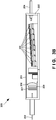
- Fig. 3B is a schematic side view showing the arrangement of the semiconductor laser module 300 according to the technical premise of the semiconductor laser module according to this example embodiment.
- the semiconductor laser module 300 includes a plurality of semiconductor laser elements 301, an optical fiber 302, lead pins 304, a housing 305, lenses 306 and 307, and an optical filter 309.
- the plurality of semiconductor laser elements 301, optical fiber 302, lead pins 304, lenses 306 and 307, and optical filter 309 are accommodated and implemented in the housing 305, thereby forming the semiconductor laser module 300.
- the housing 305 includes a top 351. Note that in the use state of the semiconductor laser module 300, the top 351 is attached to the housing 305 by adhering, screwing, or the like, thereby sealing the housing 305. The interior of the housing 305 is sealed, and thus the internal structure of the semiconductor laser module 300 cannot be seen from the outside.
- the semiconductor laser module 300 has a structure for preventing dust from entering the housing 305.
- the semiconductor laser module 300 condenses a laser beam emitted from each of the plurality of semiconductor laser elements 301, and irradiates an external target with the laser beam.
- the semiconductor laser element 301 is a high-output semiconductor laser element, and emits, for example, a high-output laser beam of 10 W or more.
- the semiconductor laser element 301 emits a laser beam having a wavelength of 900 nm to 1,000 nm. Furthermore, if it is desirable to raise the output of the laser beam emitted from the semiconductor laser module 300, this is implemented by increasing the number of semiconductor laser elements 301 or raising the output of each semiconductor laser element 301.
- the optical fiber 302 is, for example, a multi-mode optical fiber having a predetermined core diameter and cladding diameter.
- the present invention is not limited to this, and a single-mode optical fiber may be used.
- the numerical aperture (NA) of the optical fiber 302 falls within, for example, the range of 0.15 to 0.22. The present invention, however, is not limited to this.
- Each lead pin 304 supplies power to the semiconductor laser elements 301 via a bonding wire (not shown). Power may be supplied to the semiconductor laser elements 301 at a constant voltage or modulation voltage.
- Each of the lenses 306 and 307 is, for example, a cylindrical lens, and condenses a laser beam emitted from each semiconductor laser element 301, and couples it to the optical fiber 302.
- the arrangement positions of the lenses 306 and 307 with respect to the optical fiber 302 are adjusted so that the laser beam emitted from each semiconductor laser element 301 is coupled to the optical fiber 302 at a predetermined coupling ratio.
- the optical filter 309 is arranged between the lenses 306 and 307 and the optical fiber 302. If the semiconductor laser module 300 is used as, for example, an excitation light source of a fiber laser, this filter 309 is arranged for the purpose of blocking return light which enters the semiconductor laser module 300 from the fiber laser.
- the optical filter 309 is a low-pass filter, and reflects a laser beam having a wavelength of 1,060 nm to 1,080 nm and transmits a laser beam having a wavelength of 900 nm to 1,000 nm.
- the optical filter 309 prevents each semiconductor laser element 301 from being irradiated with a laser beam having a wavelength of 1,060 nm to 1,080 nm from the outside of the semiconductor laser module while transmitting a laser beam emitted from the semiconductor laser element 301.
- the optical filter 309 is arranged to form an angle with the optical axis of a laser beam reflected by the optical filter 309 so the laser beam does not return to the optical fiber 302.
- the top 351, side walls, bottom surface, and the like of the housing 305 are irradiated with light leaking from the end face of each semiconductor laser element 301, light not entering the optical fiber 302, or the like as stray light. A portion irradiated with stray light or the like is heated to raise its temperature.
- the semiconductor laser element 301 itself generates heat, and the heat is transferred to the top 351, side walls, bottom surface, and the like, thereby heating the top 351 and the like.
- the bottom surface portion and side wall portions of the housing 305 are connected to a cooling medium such as a heat sink. Even if, therefore, stray light hits the bottom surface portion and side wall portions, heat can be emitted to the heat sink side, thereby making it difficult to raise the temperature.
- the top 351 is far from the heat sink, and has a high thermal resistance.
- the top 351 is irradiated with stray light or the like, it is heated to raise its temperature, and thus extends and expands. If, for example, the top 351 extends, the whole housing 305 is distorted.
- Adjustment for guiding the laser beam to the optical fiber 302 is very severe.
- the housing 305 is distorted even slightly, the condensing position of the laser beam to the optical fiber 302 shifts.
- the coupling ratio of the laser beam emitted from the semiconductor laser element 301 to the optical fiber 302 changes, and the amount of light exiting from the semiconductor laser module 300 changes, thereby changing (decreasing) the output of the laser beam.
- FIG. 1 is a schematic side view for explaining the arrangement of the semiconductor laser module 100 according to this example embodiment.
- the semiconductor laser module 100 includes semiconductor laser elements 101, an optical fiber 102, a thin plate 103, a lead pin 104, a housing 105, lenses 106, 107, and 108, and an optical filter 109.
- the plurality of semiconductor laser elements 101, the optical fiber 102, the lead pin 104, the lenses 106, 107, and 108, and the optical filter 109 are implemented in the housing 105, thereby forming the semiconductor laser module 100.
- a laser beam output from each of the semiconductor laser elements 101 is coupled to the optical fiber 102 via an optical system formed by including the lenses 106, 107, and 108 and optical filter 109 in the housing 105.
- the laser beam coupled to the optical fiber 102 exits to the outside of the semiconductor laser module 100.
- the thin plate 103 is arranged in the housing 105, and attached on the inner surface side of a top 151. More specifically, the thin plate 103 is provided between the semiconductor laser elements 101 and the top 151, that is, at a position facing the semiconductor laser elements 101. A gap 131 is formed between the thin plate 103 and the top 151. The thin plate 103 is provided on the inner surface side of the top 151. The example in which the thin plate 103 is provided at the position facing the semiconductor laser elements 101 has been explained. However, the thin plate 103 may also be provided at a position facing the lenses 106, 107, and 108 and the optical filter 109. In this case, the number of thin plates 103 may be one or more.
- the thin plate 103 is irradiated with the stray light or return light of the laser beam output from each of the semiconductor laser elements 101, and a portion covered with the thin plate 103 of the top 151 is not directly irradiated with the stray light or return light. That is, the thin plate 103 serves as a shield against irradiation with the stray light, return light, or the like, and heat generated by the light. It becomes difficult to heat the top 151 by the stray light, thereby suppressing a rise in temperature of the top 151. Since the portion covered with the thin plate 103 of the top 151 is not heated, extension, warp, expansion, or the like of the top 151 can be suppressed, thereby making it difficult to distort the whole housing 105.
- the thin plate 103 may have a size to cover the whole top 151 or part of the top 151. Alternatively, the thin plate 103 may have a size to cover the plurality of semiconductor laser elements 101. In addition, the thin plate 103 may have a rectangular shape, a circular shape, a polygonal shape, or a shape obtained by combining some of these shapes.
- the thin plate 103 may be made of metal, preferably aluminum (Al), copper (Cu), iron (Fe), or the like, but the present invention is not limited to them. Furthermore, the material of the thin plate 103 preferably has a thermal expansion coefficient smaller than that of the material of the top 151 or the housing 105.
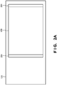
- Fig. 2A is a plan view showing the arrangement of the top 151 and thin plate 103 of the semiconductor laser module 100 according to this example embodiment.
- Fig. 2B is a partially enlarged side view showing the arrangement of the top 151 and thin plate 103 of the semiconductor laser module 100 according to this example embodiment.
- the thin plate 103 is arranged at the position to cover a portion from the center of the top 151 to its right side portion.
- the thin plate 103 has an area which covers about 2/3 of the area of the top 151 but the area of the thin plate 103 is not limited to this.
- the area of the thin plate 103 may be equal to or smaller than that of the top 151.
- the thin plate 103 has a rectangular shape, but the shape of the thin plate 103 is not limited to this.
- the thin plate 103 may have, for example, a circular shape, a polygonal shape, or a shape obtained by combining some or all of the rectangular shape, circular shape, and polygonal shape.
- the thin plate 103 preferably has a thickness of 0.1 mm to 0.2 mm, but the thickness of the thin plate 103 is not limited to this.
- the thin plate 103 is fixed to the top 151 by fixing portions 231.
- the thin plate 103 is fixed to the top 151 by, for example, adhering the fixing portions 231 using an adhesive (a thermosetting adhesive, an ultraviolet (UV) adhesive, or the like), or by screwing the fixing portions 231.
- an adhesive a thermosetting adhesive, an ultraviolet (UV) adhesive, or the like
- a rubber or resin adhesive or the like may be used as an adhesive, but the present invention is not limited to them.
- the thin plate 103 may be fixed to the top 151 by spot welding, YAG-welding, or the like.
- the thin plate 103 may be fixed to the top 151 by soldering or brazing, or using an adhesive tape.
- the two end portions of the thin plate 103 are folded to form folding portions 232. By providing the folding portions 232 at the two ends of the thin plate 103, the gap 131 is formed between the thin plate 103 and the top 151. Note that the folding portion 232 may be formed in one end portion of the
- the thin plate 103 Since the thin plate 103 is fixed to the top 151 by the two fixing portions 231, the heat of the thin plate 103 is difficult to be transferred to the top 151. Note that the thin plate 103 may be fixed to the top 151 by one fixing portion 231 or three or more fixing portions 231.
- Fig. 2C is a partially enlarged side view showing an example of the arrangement of the thin plates of the semiconductor laser module according to this example embodiment.
- the two thin plates 103 may be arranged side by side.
- the number of thin plates to be arranged is not limited to two, and may be three or more.
- Fig. 2D is a partially enlarged side view showing another example of the arrangement of the thin plate of the semiconductor laser module according to this example embodiment.
- the thin plate 103 may have a wavy shape when viewed from the side.
- the thin plate 103 can have various shapes such as upward- and downward-convex shapes when viewed from, for example, the side of the semiconductor laser module 100 on which the optical fiber 102 is provided.
- Fig. 2E is a partially enlarged side view showing still other example of the arrangement of the thin plate 103 of the semiconductor laser module according to this example embodiment.
- the thin plate 103 may have a curved shape when viewed from the side.
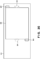
- Fig. 2F is a plan view showing an example of the arrangement of the fixing portions of the thin plate of the semiconductor laser module according to this example embodiment. As shown in Fig. 2F , part of each fixing portion 231 may be removed. That is, part (a portion indicated by dotted lines in Fig. 2F ) of each fixing portion 231 shown in Fig. 2A may be removed. In this case, the thin plate 103 is fixed to the top 151 by the four fixing portions 231.
- Fig. 2G is a plan view showing another example of the arrangement of the fixing portions of the thin plate of the semiconductor laser module according to this example embodiment.
- the thin plate 103 may be fixed to the top 151 by the two fixing portions 231.
- the two fixing portions 231 are arranged at positions on a diagonal line but may be arranged at positions (one-dot dashed lines) facing each other.
- the thin plate serves as a shield against stray light or return light, and the top of the housing is not heated, the top of the housing is difficult to warp by heating, and the housing itself is difficult to be distorted, thereby suppressing a variation in coupling ratio to the optical fiber.
- FIG. 4 is a view for explaining the arrangement of a three-dimensional laminating and shaping apparatus 400 according to this example embodiment. Note that in Fig. 4 , to avoid the view from becoming complicated, components other than those shown in Fig. 4 are not illustrated, as needed. Note also that an LMD (Laser Metal Deposition) type three-dimensional laminating and shaping apparatus will be exemplified as the three-dimensional laminating and shaping apparatus 400 but a powder bed type three-dimensional laminating and shaping apparatus may be adopted.
- LMD Laser Metal Deposition
- the three-dimensional laminating and shaping apparatus 400 is an apparatus for shaping a three-dimensional laminated and shaped object 420 on a shaping table 430 by melting and solidifying a metal powder or the like as a material of the three-dimensional laminated and shaped object by irradiating the metal powder with a laser beam, and laminating the metal powder.
- the three-dimensional laminating and shaping apparatus 400 includes a semiconductor laser module 100, the shaping table 430, a material storage 450, a material delivery tube 451, a controller 460, and a nozzle 470.
- the material storage 450, material delivery tube 451, and nozzle 470 form a material supplier.
- the semiconductor laser module 100 serving as a light source generates a light beam such as a laser beam.
- the optical path of the generated laser beam is adjusted by the semiconductor laser module 100, a lens barrel (not shown), or the like, and the shaping table 430 is irradiated with the laser beam.
- the nozzle 470 ejects a carrier gas 440 from the distal end of the nozzle 470 to supply the material of the three-dimensional laminated and shaped object 420 onto the shaping table 430.
- the carrier gas 440 is an inert gas such as argon gas, nitrogen gas, or helium gas, and is a gas for conveying the metal powder or the like as the material of the three-dimensional laminated and shaped object 420 onto the shaping table 430.
- the material storage 450 stores the material of the three-dimensional laminated and shaped object 420, and supplies the material to the nozzle 470 via the material delivery tube 451 by force feed or the like.
- the controller 460 is connected to the semiconductor laser module 100, material storage 450, and nozzle 470.
- the controller 460 controls the semiconductor laser module 100 to adjust and control the output energy, scanning direction, scanning speed, focusing state, and the like of the laser beam.
- the controller 460 controls the nozzle 470 and material storage 450 to adjust the scanning speed of the nozzle 470, the ejection amount of the carrier gas 440 from the nozzle 470, and the like, thereby adjusting the supply amount of the material.
Landscapes
- Physics & Mathematics (AREA)
- Optics & Photonics (AREA)
- General Physics & Mathematics (AREA)
- Electromagnetism (AREA)
- Condensed Matter Physics & Semiconductors (AREA)
- Engineering & Computer Science (AREA)
- Materials Engineering (AREA)
- Health & Medical Sciences (AREA)
- Manufacturing & Machinery (AREA)
- Chemical & Material Sciences (AREA)
- Toxicology (AREA)
- General Health & Medical Sciences (AREA)
- Plasma & Fusion (AREA)
- Semiconductor Lasers (AREA)
- Optical Couplings Of Light Guides (AREA)
Description
- The present invention relates to a semiconductor laser module and a three-dimensional laminating and shaping apparatus.
- In the above technical field, patent literature 1 discloses a technique of condensing a laser beam emitted from a semiconductor laser element through a lens, coupling it to an optical fiber, and externally emitting the laser beam.
- Patent literature 1: Japanese Patent Laid-Open No.
2004-96088 US 2015/183060 A1 , describing a method of manufacturing an optical module, as well as in documentJP 2004 109313 A US 7 226 222 B2 , describing a laser module with sealed packages having reduced total volume. DocumentUS 2012/320938 A1 describes a semiconductor laser module including a hermetically sealed package with increased cooling capacity. - In the technique described in the above Patent literature 1, however, it is impossible to suppress a variation in coupling ratio of output light from a semiconductor laser element to an optical fiber.
- The present invention enables to provide a technique of solving the above-described problem.
- One aspect of the present invention provides a semiconductor laser module as defined in claim 1.
- Another aspect of the present invention provides a three-dimensional laminating and shaping apparatus using the above-described semiconductor laser module. Further advantageous developments of the present invention are defined in the dependent claims.
- According to the present invention, it is possible to suppress a variation in coupling ratio of output light from a semiconductor laser element to an optical fiber.
-
-
Fig. 1 is a schematic side view showing the arrangement of a semiconductor laser module according to the first example embodiment of the present invention; -
Fig. 2A is a plan view showing an example of the arrangement of the top and thin plate of the semiconductor laser module according to the first example embodiment of the present invention; -
Fig. 2B is a partially enlarged side view showing the example of the arrangement of the top and thin plate of the semiconductor laser module according to the first example embodiment of the present invention; -
Fig. 2C is a partially enlarged side view showing an example of the arrangement of the thin plates of the semiconductor laser module according to the first example embodiment of the present invention; -
Fig. 2D is a partially enlarged side view showing another example of the arrangement of the thin plate of the semiconductor laser module according to the first example embodiment of the present invention; -
Fig. 2E is a partially enlarged side view showing still other example of the arrangement of the thin plate of the semiconductor laser module according to the first example embodiment of the present invention; -
Fig. 2F is a plan view showing an example of the arrangement of the fixing portions of the thin plate of the semiconductor laser module according to the first example embodiment of the present invention; -
Fig. 2G is a plan view showing another example of the arrangement of the fixing portions of the thin plate of the semiconductor laser module according to the first example embodiment of the present invention; -
Fig. 3A is a schematic perspective view showing the arrangement of a semiconductor laser module according to a technical premise of the semiconductor laser module according to the first example embodiment of the present invention; -
Fig. 3B is a schematic side view showing the arrangement of the semiconductor laser module according to the technical premise of the semiconductor laser module according to the first example embodiment of the present invention; and -
Fig. 4 is a view showing the arrangement of a three-dimensional laminating and shaping apparatus according to the second example embodiment of the present invention. - Example embodiments of the present invention will now be described in detail with reference to the drawings. It should be noted that the relative arrangement of the components, the numerical expressions and numerical values set forth in these example embodiments do not limit the scope of the present invention unless it is specifically stated otherwise.
- A
semiconductor laser module 100 according to the first example embodiment of the present invention will be described with reference toFig. 1 . Thesemiconductor laser module 100 is an apparatus for condensing a laser beam emitted from a semiconductor laser element through a condenser lens to enter an optical fiber, and irradiating a target outside the module with the laser beam. - A
semiconductor laser module 300 according to a technical premise of the semiconductor laser module according to this example embodiment will be described with reference toFigs. 3A and3B .Fig. 3A is a schematic perspective view showing the arrangement of thesemiconductor laser module 300 according to the technical premise of the semiconductor laser module according to this example embodiment.Fig. 3B is a schematic side view showing the arrangement of thesemiconductor laser module 300 according to the technical premise of the semiconductor laser module according to this example embodiment. - The
semiconductor laser module 300 includes a plurality ofsemiconductor laser elements 301, anoptical fiber 302,lead pins 304, ahousing 305,lenses optical filter 309. The plurality ofsemiconductor laser elements 301,optical fiber 302,lead pins 304,lenses optical filter 309 are accommodated and implemented in thehousing 305, thereby forming thesemiconductor laser module 300. - The
housing 305 includes atop 351. Note that in the use state of thesemiconductor laser module 300, thetop 351 is attached to thehousing 305 by adhering, screwing, or the like, thereby sealing thehousing 305. The interior of thehousing 305 is sealed, and thus the internal structure of thesemiconductor laser module 300 cannot be seen from the outside. Thesemiconductor laser module 300 has a structure for preventing dust from entering thehousing 305. Thesemiconductor laser module 300 condenses a laser beam emitted from each of the plurality ofsemiconductor laser elements 301, and irradiates an external target with the laser beam. - The
semiconductor laser element 301 is a high-output semiconductor laser element, and emits, for example, a high-output laser beam of 10 W or more. For example, thesemiconductor laser element 301 emits a laser beam having a wavelength of 900 nm to 1,000 nm. Furthermore, if it is desirable to raise the output of the laser beam emitted from thesemiconductor laser module 300, this is implemented by increasing the number ofsemiconductor laser elements 301 or raising the output of eachsemiconductor laser element 301. - The
optical fiber 302 is, for example, a multi-mode optical fiber having a predetermined core diameter and cladding diameter. The present invention, however, is not limited to this, and a single-mode optical fiber may be used. The numerical aperture (NA) of theoptical fiber 302 falls within, for example, the range of 0.15 to 0.22. The present invention, however, is not limited to this. - Each
lead pin 304 supplies power to thesemiconductor laser elements 301 via a bonding wire (not shown). Power may be supplied to thesemiconductor laser elements 301 at a constant voltage or modulation voltage. - Each of the
lenses semiconductor laser element 301, and couples it to theoptical fiber 302. The arrangement positions of thelenses optical fiber 302 are adjusted so that the laser beam emitted from eachsemiconductor laser element 301 is coupled to theoptical fiber 302 at a predetermined coupling ratio. - The
optical filter 309 is arranged between thelenses optical fiber 302. If thesemiconductor laser module 300 is used as, for example, an excitation light source of a fiber laser, thisfilter 309 is arranged for the purpose of blocking return light which enters thesemiconductor laser module 300 from the fiber laser. Theoptical filter 309 is a low-pass filter, and reflects a laser beam having a wavelength of 1,060 nm to 1,080 nm and transmits a laser beam having a wavelength of 900 nm to 1,000 nm. Therefore, theoptical filter 309 prevents eachsemiconductor laser element 301 from being irradiated with a laser beam having a wavelength of 1,060 nm to 1,080 nm from the outside of the semiconductor laser module while transmitting a laser beam emitted from thesemiconductor laser element 301. Theoptical filter 309 is arranged to form an angle with the optical axis of a laser beam reflected by theoptical filter 309 so the laser beam does not return to theoptical fiber 302. - In the
semiconductor laser module 300 having the above-described arrangement, the top 351, side walls, bottom surface, and the like of thehousing 305 are irradiated with light leaking from the end face of eachsemiconductor laser element 301, light not entering theoptical fiber 302, or the like as stray light. A portion irradiated with stray light or the like is heated to raise its temperature. - The
semiconductor laser element 301 itself generates heat, and the heat is transferred to the top 351, side walls, bottom surface, and the like, thereby heating the top 351 and the like. The bottom surface portion and side wall portions of thehousing 305 are connected to a cooling medium such as a heat sink. Even if, therefore, stray light hits the bottom surface portion and side wall portions, heat can be emitted to the heat sink side, thereby making it difficult to raise the temperature. - On the other hand, the top 351 is far from the heat sink, and has a high thermal resistance. Thus, if the top 351 is irradiated with stray light or the like, it is heated to raise its temperature, and thus extends and expands. If, for example, the top 351 extends, the
whole housing 305 is distorted. - Adjustment for guiding the laser beam to the
optical fiber 302 is very severe. Thus, if thehousing 305 is distorted even slightly, the condensing position of the laser beam to theoptical fiber 302 shifts. As a result, the coupling ratio of the laser beam emitted from thesemiconductor laser element 301 to theoptical fiber 302 changes, and the amount of light exiting from thesemiconductor laser module 300 changes, thereby changing (decreasing) the output of the laser beam. - A semiconductor laser module according to this example embodiment will be described with reference to
Figs. 1 to 2G .Fig. 1 is a schematic side view for explaining the arrangement of thesemiconductor laser module 100 according to this example embodiment. - As shown in
Fig. 1 , thesemiconductor laser module 100 includessemiconductor laser elements 101, anoptical fiber 102, athin plate 103, alead pin 104, ahousing 105,lenses optical filter 109. The plurality ofsemiconductor laser elements 101, theoptical fiber 102, thelead pin 104, thelenses optical filter 109 are implemented in thehousing 105, thereby forming thesemiconductor laser module 100. - A laser beam output from each of the
semiconductor laser elements 101 is coupled to theoptical fiber 102 via an optical system formed by including thelenses optical filter 109 in thehousing 105. The laser beam coupled to theoptical fiber 102 exits to the outside of thesemiconductor laser module 100. - The
thin plate 103 is arranged in thehousing 105, and attached on the inner surface side of a top 151. More specifically, thethin plate 103 is provided between thesemiconductor laser elements 101 and the top 151, that is, at a position facing thesemiconductor laser elements 101. Agap 131 is formed between thethin plate 103 and the top 151. Thethin plate 103 is provided on the inner surface side of the top 151. The example in which thethin plate 103 is provided at the position facing thesemiconductor laser elements 101 has been explained. However, thethin plate 103 may also be provided at a position facing thelenses optical filter 109. In this case, the number ofthin plates 103 may be one or more. - The
thin plate 103 is irradiated with the stray light or return light of the laser beam output from each of thesemiconductor laser elements 101, and a portion covered with thethin plate 103 of the top 151 is not directly irradiated with the stray light or return light. That is, thethin plate 103 serves as a shield against irradiation with the stray light, return light, or the like, and heat generated by the light. It becomes difficult to heat the top 151 by the stray light, thereby suppressing a rise in temperature of the top 151. Since the portion covered with thethin plate 103 of the top 151 is not heated, extension, warp, expansion, or the like of the top 151 can be suppressed, thereby making it difficult to distort thewhole housing 105. - The
thin plate 103 may have a size to cover the whole top 151 or part of the top 151. Alternatively, thethin plate 103 may have a size to cover the plurality ofsemiconductor laser elements 101. In addition, thethin plate 103 may have a rectangular shape, a circular shape, a polygonal shape, or a shape obtained by combining some of these shapes. - The
thin plate 103 may be made of metal, preferably aluminum (Al), copper (Cu), iron (Fe), or the like, but the present invention is not limited to them. Furthermore, the material of thethin plate 103 preferably has a thermal expansion coefficient smaller than that of the material of the top 151 or thehousing 105. -
Fig. 2A is a plan view showing the arrangement of the top 151 andthin plate 103 of thesemiconductor laser module 100 according to this example embodiment.Fig. 2B is a partially enlarged side view showing the arrangement of the top 151 andthin plate 103 of thesemiconductor laser module 100 according to this example embodiment. - As shown in
Figs. 2A and2B , thethin plate 103 is arranged at the position to cover a portion from the center of the top 151 to its right side portion. Thethin plate 103 has an area which covers about 2/3 of the area of the top 151 but the area of thethin plate 103 is not limited to this. For example, the area of thethin plate 103 may be equal to or smaller than that of the top 151. - Furthermore, the
thin plate 103 has a rectangular shape, but the shape of thethin plate 103 is not limited to this. Thethin plate 103 may have, for example, a circular shape, a polygonal shape, or a shape obtained by combining some or all of the rectangular shape, circular shape, and polygonal shape. - The
thin plate 103 preferably has a thickness of 0.1 mm to 0.2 mm, but the thickness of thethin plate 103 is not limited to this. - The
thin plate 103 is fixed to the top 151 by fixingportions 231. Thethin plate 103 is fixed to the top 151 by, for example, adhering the fixingportions 231 using an adhesive (a thermosetting adhesive, an ultraviolet (UV) adhesive, or the like), or by screwing the fixingportions 231. For example, a rubber or resin adhesive or the like may be used as an adhesive, but the present invention is not limited to them. Furthermore, thethin plate 103 may be fixed to the top 151 by spot welding, YAG-welding, or the like. Alternatively, thethin plate 103 may be fixed to the top 151 by soldering or brazing, or using an adhesive tape. The two end portions of thethin plate 103 are folded to formfolding portions 232. By providing thefolding portions 232 at the two ends of thethin plate 103, thegap 131 is formed between thethin plate 103 and the top 151. Note that thefolding portion 232 may be formed in one end portion of thethin plate 103. - Since the
thin plate 103 is fixed to the top 151 by the two fixingportions 231, the heat of thethin plate 103 is difficult to be transferred to the top 151. Note that thethin plate 103 may be fixed to the top 151 by one fixingportion 231 or three ormore fixing portions 231. -
Fig. 2C is a partially enlarged side view showing an example of the arrangement of the thin plates of the semiconductor laser module according to this example embodiment. As shown inFig. 2C , the twothin plates 103 may be arranged side by side. The number of thin plates to be arranged is not limited to two, and may be three or more. -
Fig. 2D is a partially enlarged side view showing another example of the arrangement of the thin plate of the semiconductor laser module according to this example embodiment. Thethin plate 103 may have a wavy shape when viewed from the side. As other examples, thethin plate 103 can have various shapes such as upward- and downward-convex shapes when viewed from, for example, the side of thesemiconductor laser module 100 on which theoptical fiber 102 is provided. -
Fig. 2E is a partially enlarged side view showing still other example of the arrangement of thethin plate 103 of the semiconductor laser module according to this example embodiment. Thethin plate 103 may have a curved shape when viewed from the side. -
Fig. 2F is a plan view showing an example of the arrangement of the fixing portions of the thin plate of the semiconductor laser module according to this example embodiment. As shown inFig. 2F , part of each fixingportion 231 may be removed. That is, part (a portion indicated by dotted lines inFig. 2F ) of each fixingportion 231 shown inFig. 2A may be removed. In this case, thethin plate 103 is fixed to the top 151 by the four fixingportions 231. -
Fig. 2G is a plan view showing another example of the arrangement of the fixing portions of the thin plate of the semiconductor laser module according to this example embodiment. As shown inFig. 2G , thethin plate 103 may be fixed to the top 151 by the two fixingportions 231. In this case, the two fixingportions 231 are arranged at positions on a diagonal line but may be arranged at positions (one-dot dashed lines) facing each other. - According to this example embodiment, it is possible to suppress a variation in coupling ratio of output light from each semiconductor laser element to the optical fiber. In addition, since the thin plate serves as a shield against stray light or return light, and the top of the housing is not heated, the top of the housing is difficult to warp by heating, and the housing itself is difficult to be distorted, thereby suppressing a variation in coupling ratio to the optical fiber.
- A three-dimensional laminating and shaping apparatus according to the second example embodiment of the present invention will be described next with reference to
Fig. 4. Fig. 4 is a view for explaining the arrangement of a three-dimensional laminating and shapingapparatus 400 according to this example embodiment. Note that inFig. 4 , to avoid the view from becoming complicated, components other than those shown inFig. 4 are not illustrated, as needed. Note also that an LMD (Laser Metal Deposition) type three-dimensional laminating and shaping apparatus will be exemplified as the three-dimensional laminating and shapingapparatus 400 but a powder bed type three-dimensional laminating and shaping apparatus may be adopted. - The three-dimensional laminating and shaping
apparatus 400 is an apparatus for shaping a three-dimensional laminated and shapedobject 420 on a shaping table 430 by melting and solidifying a metal powder or the like as a material of the three-dimensional laminated and shaped object by irradiating the metal powder with a laser beam, and laminating the metal powder. - As shown in
Fig. 4 , the three-dimensional laminating and shapingapparatus 400 includes asemiconductor laser module 100, the shaping table 430, amaterial storage 450, amaterial delivery tube 451, acontroller 460, and anozzle 470. Thematerial storage 450,material delivery tube 451, andnozzle 470 form a material supplier. - The
semiconductor laser module 100 serving as a light source generates a light beam such as a laser beam. The optical path of the generated laser beam is adjusted by thesemiconductor laser module 100, a lens barrel (not shown), or the like, and the shaping table 430 is irradiated with the laser beam. Thenozzle 470 ejects acarrier gas 440 from the distal end of thenozzle 470 to supply the material of the three-dimensional laminated and shapedobject 420 onto the shaping table 430. Thecarrier gas 440 is an inert gas such as argon gas, nitrogen gas, or helium gas, and is a gas for conveying the metal powder or the like as the material of the three-dimensional laminated and shapedobject 420 onto the shaping table 430. Thematerial storage 450 stores the material of the three-dimensional laminated and shapedobject 420, and supplies the material to thenozzle 470 via thematerial delivery tube 451 by force feed or the like. - The
controller 460 is connected to thesemiconductor laser module 100,material storage 450, andnozzle 470. Thecontroller 460 controls thesemiconductor laser module 100 to adjust and control the output energy, scanning direction, scanning speed, focusing state, and the like of the laser beam. Furthermore, thecontroller 460 controls thenozzle 470 andmaterial storage 450 to adjust the scanning speed of thenozzle 470, the ejection amount of thecarrier gas 440 from thenozzle 470, and the like, thereby adjusting the supply amount of the material. - According to this example embodiment, since a semiconductor laser module in which the coupling ratio of a laser beam does not lower is used, it is possible to shape a more accurate three-dimensional laminated and shaped object.
- While the invention has been particularly shown and described with reference to example embodiments thereof, the invention is not limited to these example embodiments. It will be understood by those of ordinary skill in the art that various changes in form and details may be made therein without departing from the scope of the present invention as defined by the claims.
Claims (9)
- A semiconductor laser module (100) including a plurality of semiconductor laser elements (101), an optical fiber (102), a condenser (106,107) that condenses a laser beam emitted from each of said semiconductor laser elements to said optical fiber, and a housing (105) that implements and accommodates therein said laser elements, said condenser, and an input end of said optical fiber, the semiconductor laser module comprising: at least one thin plate (103) that is arranged between said laser elements and a top (151) of said housing, and is attached inside said housing to the inner surface side of said top of said housing to form a gap (131) with said top of said housing for shielding said top of said housing from heat generated by the laser beam.
- The semiconductor laser module according to claim 1, wherein said thin plate includes a folding portion (232) in at least one end portion, and is arranged on the top via said folding portion so that the gap is formed.
- The semiconductor laser module according to claim 1 or 2, wherein said thin plate is provided at a position facing only said semiconductor laser elements.
- The semiconductor laser module according to claim 1 or 2, wherein said thin plate has a size to cover at least part of the top.
- The semiconductor laser module according to any one of claims 1 to 3, wherein said thin plate has a size to cover said plurality of semiconductor laser elements.
- The semiconductor laser module according to any one of claims 1 to 5, wherein said thin plate has one of a rectangular shape, a circular shape, and a polygonal shape.
- The semiconductor laser module according to any one of claims 1 to 6, wherein said thin plate has a thickness of 0.1 mm to 0.2 mm.
- The semiconductor laser module according to any one of claims 1 to 7, wherein said thin plate is made of aluminum.
- A three-dimensional laminating and shaping apparatus (400) using a semiconductor laser module defined in any one of claims 1 to 8.
Applications Claiming Priority (1)
| Application Number | Priority Date | Filing Date | Title |
|---|---|---|---|
| PCT/JP2016/077102 WO2018051430A1 (en) | 2016-09-14 | 2016-09-14 | Semiconductor laser module and additive manufacturing device |
Publications (3)
| Publication Number | Publication Date |
|---|---|
| EP3324229A1 EP3324229A1 (en) | 2018-05-23 |
| EP3324229A4 EP3324229A4 (en) | 2018-10-24 |
| EP3324229B1 true EP3324229B1 (en) | 2019-12-18 |
Family
ID=61619927
Family Applications (1)
| Application Number | Title | Priority Date | Filing Date |
|---|---|---|---|
| EP16885450.3A Active EP3324229B1 (en) | 2016-09-14 | 2016-09-14 | Semiconductor laser module and additive manufacturing device |
Country Status (4)
| Country | Link |
|---|---|
| US (1) | US10234645B2 (en) |
| EP (1) | EP3324229B1 (en) |
| JP (1) | JP6383866B2 (en) |
| WO (1) | WO2018051430A1 (en) |
Families Citing this family (3)
| Publication number | Priority date | Publication date | Assignee | Title |
|---|---|---|---|---|
| JP6765395B2 (en) | 2018-06-14 | 2020-10-07 | 株式会社フジクラ | Optical module unit and laser device |
| CN112072458A (en) * | 2019-06-11 | 2020-12-11 | 南昌欧菲生物识别技术有限公司 | Base, light emission module, 3D recognition device and intelligent terminal |
| JP7623150B2 (en) * | 2021-02-05 | 2025-01-28 | 古河電気工業株式会社 | Optical device, light source device, and optical fiber laser |
Family Cites Families (20)
| Publication number | Priority date | Publication date | Assignee | Title |
|---|---|---|---|---|
| JPH06138351A (en) * | 1992-10-30 | 1994-05-20 | Tokimec Inc | Light source device |
| JP2003142767A (en) * | 2001-10-31 | 2003-05-16 | Furukawa Electric Co Ltd:The | Laser module |
| US6856475B2 (en) * | 2001-10-31 | 2005-02-15 | The Furukawa Electric Co., Ltd | Optical module having temperature adjustment features |
| JP2004006440A (en) * | 2002-04-10 | 2004-01-08 | Fuji Photo Film Co Ltd | Laser apparatus, exposure head, and exposure device |
| US6960035B2 (en) | 2002-04-10 | 2005-11-01 | Fuji Photo Film Co., Ltd. | Laser apparatus, exposure head, exposure apparatus, and optical fiber connection method |
| JP3896905B2 (en) * | 2002-06-18 | 2007-03-22 | 住友電気工業株式会社 | Optical communication device |
| US7830945B2 (en) * | 2002-07-10 | 2010-11-09 | Fujifilm Corporation | Laser apparatus in which laser diodes and corresponding collimator lenses are fixed to block, and fiber module in which laser apparatus is coupled to optical fiber |
| JP2004096088A (en) | 2002-07-10 | 2004-03-25 | Fuji Photo Film Co Ltd | Combined laser light source and exposure apparatus |
| JP2004109313A (en) * | 2002-09-17 | 2004-04-08 | Ricoh Co Ltd | Optical transmission / reception device and information transmission device |
| JP2006054366A (en) * | 2004-08-13 | 2006-02-23 | Fuji Photo Film Co Ltd | Laser module |
| JP2006267237A (en) * | 2005-03-22 | 2006-10-05 | Fuji Photo Film Co Ltd | Laser device and its assembling method and its attachment structure |
| US8401047B2 (en) * | 2010-03-10 | 2013-03-19 | Panasonic Corporation | Semiconductor laser device |
| JP5583632B2 (en) * | 2011-05-13 | 2014-09-03 | Nttエレクトロニクス株式会社 | Optical module |
| JP2012070007A (en) * | 2011-12-26 | 2012-04-05 | Furukawa Electric Co Ltd:The | Semiconductor laser module |
| JP5717714B2 (en) * | 2012-12-27 | 2015-05-13 | 株式会社フジクラ | Multiplexing device, multiplexing method, and LD module |
| US9235015B2 (en) * | 2013-02-26 | 2016-01-12 | Avago Technologies General Ip (Singapore) Pte. Ltd. | Heat dissipation device and method for use in an optical communications module |
| EP3045947B1 (en) * | 2013-09-12 | 2019-12-04 | Furukawa Electric Co., Ltd. | Semiconductor laser module |
| JP5834125B1 (en) | 2014-09-29 | 2015-12-16 | 株式会社フジクラ | Optical fiber module |
| US10158210B2 (en) * | 2014-12-17 | 2018-12-18 | Nlight, Inc. | Optical loss management in high power diode laser packages |
| JP6457864B2 (en) * | 2015-03-30 | 2019-01-23 | 京セラ株式会社 | Optical semiconductor device package and optical semiconductor device |
-
2016
- 2016-09-14 US US15/513,371 patent/US10234645B2/en active Active
- 2016-09-14 WO PCT/JP2016/077102 patent/WO2018051430A1/en not_active Ceased
- 2016-09-14 EP EP16885450.3A patent/EP3324229B1/en active Active
- 2016-09-14 JP JP2017514583A patent/JP6383866B2/en active Active
Non-Patent Citations (1)
| Title |
|---|
| None * |
Also Published As
| Publication number | Publication date |
|---|---|
| JP6383866B2 (en) | 2018-08-29 |
| US20180231724A1 (en) | 2018-08-16 |
| EP3324229A1 (en) | 2018-05-23 |
| EP3324229A4 (en) | 2018-10-24 |
| US10234645B2 (en) | 2019-03-19 |
| JPWO2018051430A1 (en) | 2018-09-13 |
| WO2018051430A1 (en) | 2018-03-22 |
Similar Documents
| Publication | Publication Date | Title |
|---|---|---|
| EP3700030B1 (en) | Light source device, direct diode laser system, and optical coupling device | |
| US10985525B2 (en) | Transmitter module | |
| JP6230720B2 (en) | Optical component, optical module, and method of manufacturing optical component | |
| US8477822B2 (en) | Compact transistor outline packaged laser with optical monitoring function | |
| US11679448B2 (en) | Beam-forming units with cooling systems for high-power lasers | |
| US10234645B2 (en) | Semiconductor laser module and three-dimensional laminating and shaping apparatus | |
| US20140161391A1 (en) | Optical module and optical transmission method | |
| JP7190065B2 (en) | Light emitting device, light source unit, light source device, and optical fiber laser | |
| US7444047B2 (en) | Multiplexing optical system | |
| JP6753478B2 (en) | Optical module | |
| US20190341745A1 (en) | Laser device | |
| JP2021136256A (en) | Light source device and direct diode laser device | |
| JP7525780B2 (en) | Light source unit | |
| JP2016102864A (en) | Optical module and method for manufacturing the same | |
| JP7516351B2 (en) | Optical Components and Semiconductor Laser Modules | |
| JP6894485B2 (en) | Soldering equipment and its system controller | |
| US7125175B2 (en) | Optical coupling devices | |
| WO2022168934A1 (en) | Optical device, light source device, and optical fiber laser | |
| US7909518B2 (en) | Optical assembly connecting a laser with optical fibre | |
| JP7608187B2 (en) | Method for manufacturing a light emitting device | |
| JP7041362B2 (en) | Light source unit | |
| Wang et al. | Kilowatt line beam from a 905nm pulsed diode laser module for LiDAR applications | |
| JP2017098335A (en) | Wavelength multiplexing laser diode module | |
| TW201707182A (en) | Apparatus and method for laser processing | |
| JP7623237B2 (en) | Optical device, light source device, and optical fiber laser |
Legal Events
| Date | Code | Title | Description |
|---|---|---|---|
| STAA | Information on the status of an ep patent application or granted ep patent |
Free format text: STATUS: UNKNOWN |
|
| STAA | Information on the status of an ep patent application or granted ep patent |
Free format text: STATUS: THE INTERNATIONAL PUBLICATION HAS BEEN MADE |
|
| PUAI | Public reference made under article 153(3) epc to a published international application that has entered the european phase |
Free format text: ORIGINAL CODE: 0009012 |
|
| STAA | Information on the status of an ep patent application or granted ep patent |
Free format text: STATUS: REQUEST FOR EXAMINATION WAS MADE |
|
| 17P | Request for examination filed |
Effective date: 20170726 |
|
| AK | Designated contracting states |
Kind code of ref document: A1 Designated state(s): AL AT BE BG CH CY CZ DE DK EE ES FI FR GB GR HR HU IE IS IT LI LT LU LV MC MK MT NL NO PL PT RO RS SE SI SK SM TR |
|
| AX | Request for extension of the european patent |
Extension state: BA ME |
|
| A4 | Supplementary search report drawn up and despatched |
Effective date: 20180921 |
|
| RIC1 | Information provided on ipc code assigned before grant |
Ipc: H01S 5/40 20060101ALI20180917BHEP Ipc: G02B 27/09 20060101ALI20180917BHEP Ipc: H01S 5/022 20060101ALI20180917BHEP Ipc: B22F 3/105 20060101ALN20180917BHEP Ipc: H01S 5/024 20060101ALI20180917BHEP Ipc: G02B 19/00 20060101ALI20180917BHEP Ipc: G02B 6/42 20060101AFI20180917BHEP Ipc: H01S 5/00 20060101ALN20180917BHEP |
|
| RIC1 | Information provided on ipc code assigned before grant |
Ipc: H01S 5/024 20060101ALI20190430BHEP Ipc: G02B 27/09 20060101ALI20190430BHEP Ipc: H01S 5/00 20060101ALN20190430BHEP Ipc: G02B 6/42 20060101AFI20190430BHEP Ipc: G02B 19/00 20060101ALI20190430BHEP Ipc: H01S 5/022 20060101ALI20190430BHEP Ipc: B22F 3/105 20060101ALN20190430BHEP Ipc: H01S 5/40 20060101ALI20190430BHEP |
|
| GRAP | Despatch of communication of intention to grant a patent |
Free format text: ORIGINAL CODE: EPIDOSNIGR1 |
|
| RIC1 | Information provided on ipc code assigned before grant |
Ipc: H01S 5/00 20060101ALN20190523BHEP Ipc: H01S 5/40 20060101ALI20190523BHEP Ipc: G02B 6/42 20060101AFI20190523BHEP Ipc: H01S 5/024 20060101ALI20190523BHEP Ipc: G02B 19/00 20060101ALI20190523BHEP Ipc: B22F 3/105 20060101ALN20190523BHEP Ipc: H01S 5/022 20060101ALI20190523BHEP Ipc: G02B 27/09 20060101ALI20190523BHEP |
|
| STAA | Information on the status of an ep patent application or granted ep patent |
Free format text: STATUS: GRANT OF PATENT IS INTENDED |
|
| DAV | Request for validation of the european patent (deleted) | ||
| DAX | Request for extension of the european patent (deleted) | ||
| INTG | Intention to grant announced |
Effective date: 20190627 |
|
| GRAS | Grant fee paid |
Free format text: ORIGINAL CODE: EPIDOSNIGR3 |
|
| GRAA | (expected) grant |
Free format text: ORIGINAL CODE: 0009210 |
|
| STAA | Information on the status of an ep patent application or granted ep patent |
Free format text: STATUS: THE PATENT HAS BEEN GRANTED |
|
| AK | Designated contracting states |
Kind code of ref document: B1 Designated state(s): AL AT BE BG CH CY CZ DE DK EE ES FI FR GB GR HR HU IE IS IT LI LT LU LV MC MK MT NL NO PL PT RO RS SE SI SK SM TR |
|
| REG | Reference to a national code |
Ref country code: CH Ref legal event code: EP |
|
| REG | Reference to a national code |
Ref country code: IE Ref legal event code: FG4D |
|
| REG | Reference to a national code |
Ref country code: DE Ref legal event code: R096 Ref document number: 602016026637 Country of ref document: DE |
|
| REG | Reference to a national code |
Ref country code: AT Ref legal event code: REF Ref document number: 1215258 Country of ref document: AT Kind code of ref document: T Effective date: 20200115 |
|
| REG | Reference to a national code |
Ref country code: NL Ref legal event code: MP Effective date: 20191218 |
|
| PG25 | Lapsed in a contracting state [announced via postgrant information from national office to epo] |
Ref country code: LV Free format text: LAPSE BECAUSE OF FAILURE TO SUBMIT A TRANSLATION OF THE DESCRIPTION OR TO PAY THE FEE WITHIN THE PRESCRIBED TIME-LIMIT Effective date: 20191218 Ref country code: SE Free format text: LAPSE BECAUSE OF FAILURE TO SUBMIT A TRANSLATION OF THE DESCRIPTION OR TO PAY THE FEE WITHIN THE PRESCRIBED TIME-LIMIT Effective date: 20191218 Ref country code: FI Free format text: LAPSE BECAUSE OF FAILURE TO SUBMIT A TRANSLATION OF THE DESCRIPTION OR TO PAY THE FEE WITHIN THE PRESCRIBED TIME-LIMIT Effective date: 20191218 Ref country code: BG Free format text: LAPSE BECAUSE OF FAILURE TO SUBMIT A TRANSLATION OF THE DESCRIPTION OR TO PAY THE FEE WITHIN THE PRESCRIBED TIME-LIMIT Effective date: 20200318 Ref country code: GR Free format text: LAPSE BECAUSE OF FAILURE TO SUBMIT A TRANSLATION OF THE DESCRIPTION OR TO PAY THE FEE WITHIN THE PRESCRIBED TIME-LIMIT Effective date: 20200319 Ref country code: NO Free format text: LAPSE BECAUSE OF FAILURE TO SUBMIT A TRANSLATION OF THE DESCRIPTION OR TO PAY THE FEE WITHIN THE PRESCRIBED TIME-LIMIT Effective date: 20200318 Ref country code: LT Free format text: LAPSE BECAUSE OF FAILURE TO SUBMIT A TRANSLATION OF THE DESCRIPTION OR TO PAY THE FEE WITHIN THE PRESCRIBED TIME-LIMIT Effective date: 20191218 |
|
| REG | Reference to a national code |
Ref country code: LT Ref legal event code: MG4D |
|
| PG25 | Lapsed in a contracting state [announced via postgrant information from national office to epo] |
Ref country code: HR Free format text: LAPSE BECAUSE OF FAILURE TO SUBMIT A TRANSLATION OF THE DESCRIPTION OR TO PAY THE FEE WITHIN THE PRESCRIBED TIME-LIMIT Effective date: 20191218 Ref country code: RS Free format text: LAPSE BECAUSE OF FAILURE TO SUBMIT A TRANSLATION OF THE DESCRIPTION OR TO PAY THE FEE WITHIN THE PRESCRIBED TIME-LIMIT Effective date: 20191218 |
|
| PG25 | Lapsed in a contracting state [announced via postgrant information from national office to epo] |
Ref country code: AL Free format text: LAPSE BECAUSE OF FAILURE TO SUBMIT A TRANSLATION OF THE DESCRIPTION OR TO PAY THE FEE WITHIN THE PRESCRIBED TIME-LIMIT Effective date: 20191218 |
|
| PG25 | Lapsed in a contracting state [announced via postgrant information from national office to epo] |
Ref country code: RO Free format text: LAPSE BECAUSE OF FAILURE TO SUBMIT A TRANSLATION OF THE DESCRIPTION OR TO PAY THE FEE WITHIN THE PRESCRIBED TIME-LIMIT Effective date: 20191218 Ref country code: CZ Free format text: LAPSE BECAUSE OF FAILURE TO SUBMIT A TRANSLATION OF THE DESCRIPTION OR TO PAY THE FEE WITHIN THE PRESCRIBED TIME-LIMIT Effective date: 20191218 Ref country code: PT Free format text: LAPSE BECAUSE OF FAILURE TO SUBMIT A TRANSLATION OF THE DESCRIPTION OR TO PAY THE FEE WITHIN THE PRESCRIBED TIME-LIMIT Effective date: 20200513 Ref country code: EE Free format text: LAPSE BECAUSE OF FAILURE TO SUBMIT A TRANSLATION OF THE DESCRIPTION OR TO PAY THE FEE WITHIN THE PRESCRIBED TIME-LIMIT Effective date: 20191218 Ref country code: NL Free format text: LAPSE BECAUSE OF FAILURE TO SUBMIT A TRANSLATION OF THE DESCRIPTION OR TO PAY THE FEE WITHIN THE PRESCRIBED TIME-LIMIT Effective date: 20191218 |
|
| PG25 | Lapsed in a contracting state [announced via postgrant information from national office to epo] |
Ref country code: IS Free format text: LAPSE BECAUSE OF FAILURE TO SUBMIT A TRANSLATION OF THE DESCRIPTION OR TO PAY THE FEE WITHIN THE PRESCRIBED TIME-LIMIT Effective date: 20200418 Ref country code: SM Free format text: LAPSE BECAUSE OF FAILURE TO SUBMIT A TRANSLATION OF THE DESCRIPTION OR TO PAY THE FEE WITHIN THE PRESCRIBED TIME-LIMIT Effective date: 20191218 Ref country code: SK Free format text: LAPSE BECAUSE OF FAILURE TO SUBMIT A TRANSLATION OF THE DESCRIPTION OR TO PAY THE FEE WITHIN THE PRESCRIBED TIME-LIMIT Effective date: 20191218 |
|
| REG | Reference to a national code |
Ref country code: DE Ref legal event code: R097 Ref document number: 602016026637 Country of ref document: DE |
|
| REG | Reference to a national code |
Ref country code: AT Ref legal event code: MK05 Ref document number: 1215258 Country of ref document: AT Kind code of ref document: T Effective date: 20191218 |
|
| PLBE | No opposition filed within time limit |
Free format text: ORIGINAL CODE: 0009261 |
|
| STAA | Information on the status of an ep patent application or granted ep patent |
Free format text: STATUS: NO OPPOSITION FILED WITHIN TIME LIMIT |
|
| PG25 | Lapsed in a contracting state [announced via postgrant information from national office to epo] |
Ref country code: ES Free format text: LAPSE BECAUSE OF FAILURE TO SUBMIT A TRANSLATION OF THE DESCRIPTION OR TO PAY THE FEE WITHIN THE PRESCRIBED TIME-LIMIT Effective date: 20191218 Ref country code: DK Free format text: LAPSE BECAUSE OF FAILURE TO SUBMIT A TRANSLATION OF THE DESCRIPTION OR TO PAY THE FEE WITHIN THE PRESCRIBED TIME-LIMIT Effective date: 20191218 |
|
| 26N | No opposition filed |
Effective date: 20200921 |
|
| PG25 | Lapsed in a contracting state [announced via postgrant information from national office to epo] |
Ref country code: SI Free format text: LAPSE BECAUSE OF FAILURE TO SUBMIT A TRANSLATION OF THE DESCRIPTION OR TO PAY THE FEE WITHIN THE PRESCRIBED TIME-LIMIT Effective date: 20191218 Ref country code: AT Free format text: LAPSE BECAUSE OF FAILURE TO SUBMIT A TRANSLATION OF THE DESCRIPTION OR TO PAY THE FEE WITHIN THE PRESCRIBED TIME-LIMIT Effective date: 20191218 |
|
| PG25 | Lapsed in a contracting state [announced via postgrant information from national office to epo] |
Ref country code: IT Free format text: LAPSE BECAUSE OF FAILURE TO SUBMIT A TRANSLATION OF THE DESCRIPTION OR TO PAY THE FEE WITHIN THE PRESCRIBED TIME-LIMIT Effective date: 20191218 |
|
| PG25 | Lapsed in a contracting state [announced via postgrant information from national office to epo] |
Ref country code: PL Free format text: LAPSE BECAUSE OF FAILURE TO SUBMIT A TRANSLATION OF THE DESCRIPTION OR TO PAY THE FEE WITHIN THE PRESCRIBED TIME-LIMIT Effective date: 20191218 |
|
| REG | Reference to a national code |
Ref country code: CH Ref legal event code: PL |
|
| GBPC | Gb: european patent ceased through non-payment of renewal fee |
Effective date: 20200914 |
|
| REG | Reference to a national code |
Ref country code: BE Ref legal event code: MM Effective date: 20200930 |
|
| PG25 | Lapsed in a contracting state [announced via postgrant information from national office to epo] |
Ref country code: LU Free format text: LAPSE BECAUSE OF NON-PAYMENT OF DUE FEES Effective date: 20200914 |
|
| PG25 | Lapsed in a contracting state [announced via postgrant information from national office to epo] |
Ref country code: FR Free format text: LAPSE BECAUSE OF NON-PAYMENT OF DUE FEES Effective date: 20200930 |
|
| PG25 | Lapsed in a contracting state [announced via postgrant information from national office to epo] |
Ref country code: BE Free format text: LAPSE BECAUSE OF NON-PAYMENT OF DUE FEES Effective date: 20200930 Ref country code: CH Free format text: LAPSE BECAUSE OF NON-PAYMENT OF DUE FEES Effective date: 20200930 Ref country code: GB Free format text: LAPSE BECAUSE OF NON-PAYMENT OF DUE FEES Effective date: 20200914 Ref country code: LI Free format text: LAPSE BECAUSE OF NON-PAYMENT OF DUE FEES Effective date: 20200930 Ref country code: IE Free format text: LAPSE BECAUSE OF NON-PAYMENT OF DUE FEES Effective date: 20200914 |
|
| REG | Reference to a national code |
Ref country code: DE Ref legal event code: R081 Ref document number: 602016026637 Country of ref document: DE Owner name: FURUKAWA ELECTRIC CO., LTD., JP Free format text: FORMER OWNER: TECHNOLOGY RESEARCH ASSOCIATION FOR FUTURE ADDITIVE MANUFACTURING, TOKYO, JP |
|
| PG25 | Lapsed in a contracting state [announced via postgrant information from national office to epo] |
Ref country code: TR Free format text: LAPSE BECAUSE OF FAILURE TO SUBMIT A TRANSLATION OF THE DESCRIPTION OR TO PAY THE FEE WITHIN THE PRESCRIBED TIME-LIMIT Effective date: 20191218 Ref country code: MT Free format text: LAPSE BECAUSE OF FAILURE TO SUBMIT A TRANSLATION OF THE DESCRIPTION OR TO PAY THE FEE WITHIN THE PRESCRIBED TIME-LIMIT Effective date: 20191218 Ref country code: CY Free format text: LAPSE BECAUSE OF FAILURE TO SUBMIT A TRANSLATION OF THE DESCRIPTION OR TO PAY THE FEE WITHIN THE PRESCRIBED TIME-LIMIT Effective date: 20191218 |
|
| PG25 | Lapsed in a contracting state [announced via postgrant information from national office to epo] |
Ref country code: MK Free format text: LAPSE BECAUSE OF FAILURE TO SUBMIT A TRANSLATION OF THE DESCRIPTION OR TO PAY THE FEE WITHIN THE PRESCRIBED TIME-LIMIT Effective date: 20191218 Ref country code: MC Free format text: LAPSE BECAUSE OF FAILURE TO SUBMIT A TRANSLATION OF THE DESCRIPTION OR TO PAY THE FEE WITHIN THE PRESCRIBED TIME-LIMIT Effective date: 20191218 |
|
| P01 | Opt-out of the competence of the unified patent court (upc) registered |
Effective date: 20230512 |
|
| PGFP | Annual fee paid to national office [announced via postgrant information from national office to epo] |
Ref country code: DE Payment date: 20250730 Year of fee payment: 10 |