EP3324166A1 - Force sensing - Google Patents
Force sensing Download PDFInfo
- Publication number
- EP3324166A1 EP3324166A1 EP16199920.6A EP16199920A EP3324166A1 EP 3324166 A1 EP3324166 A1 EP 3324166A1 EP 16199920 A EP16199920 A EP 16199920A EP 3324166 A1 EP3324166 A1 EP 3324166A1
- Authority
- EP
- European Patent Office
- Prior art keywords
- elastic
- elastic element
- electromagnetic radiation
- optical elements
- force
- Prior art date
- Legal status (The legal status is an assumption and is not a legal conclusion. Google has not performed a legal analysis and makes no representation as to the accuracy of the status listed.)
- Withdrawn
Links
- 230000005670 electromagnetic radiation Effects 0.000 claims abstract description 29
- 230000003287 optical effect Effects 0.000 claims abstract description 21
- 239000013013 elastic material Substances 0.000 claims abstract description 10
- 239000012780 transparent material Substances 0.000 claims abstract description 6
- 230000004044 response Effects 0.000 claims abstract description 5
- 230000008859 change Effects 0.000 claims description 12
- 238000004891 communication Methods 0.000 claims description 9
- 238000003384 imaging method Methods 0.000 claims description 7
- 238000000034 method Methods 0.000 claims description 7
- 238000004590 computer program Methods 0.000 claims description 5
- 229920000426 Microplastic Polymers 0.000 claims description 3
- 241000907663 Siproeta stelenes Species 0.000 claims description 3
- 239000005030 aluminium foil Substances 0.000 claims description 3
- 239000002245 particle Substances 0.000 claims description 3
- 230000000694 effects Effects 0.000 description 6
- 230000006870 function Effects 0.000 description 4
- 239000000463 material Substances 0.000 description 3
- 230000009471 action Effects 0.000 description 1
- 238000004364 calculation method Methods 0.000 description 1
- 230000001413 cellular effect Effects 0.000 description 1
- 238000013500 data storage Methods 0.000 description 1
- 230000001419 dependent effect Effects 0.000 description 1
- 239000003989 dielectric material Substances 0.000 description 1
- 238000005516 engineering process Methods 0.000 description 1
- 230000036541 health Effects 0.000 description 1
- 238000004519 manufacturing process Methods 0.000 description 1
- 238000012986 modification Methods 0.000 description 1
- 230000004048 modification Effects 0.000 description 1
- 238000012544 monitoring process Methods 0.000 description 1
- 210000003205 muscle Anatomy 0.000 description 1
- 239000003973 paint Substances 0.000 description 1
- 229920000642 polymer Polymers 0.000 description 1
- 230000029058 respiratory gaseous exchange Effects 0.000 description 1
- 230000035945 sensitivity Effects 0.000 description 1
- 239000007784 solid electrolyte Substances 0.000 description 1
Images


Classifications
-
- G—PHYSICS
- G01—MEASURING; TESTING
- G01L—MEASURING FORCE, STRESS, TORQUE, WORK, MECHANICAL POWER, MECHANICAL EFFICIENCY, OR FLUID PRESSURE
- G01L1/00—Measuring force or stress, in general
- G01L1/24—Measuring force or stress, in general by measuring variations of optical properties of material when it is stressed, e.g. by photoelastic stress analysis using infrared, visible light, ultraviolet
Definitions
- the present application generally relates to force sensing.
- the application relates to differential force sensing.
- Force sensing is a technical field in which new applications of sensing technology require sensitive and robust force sensors at low cost, either for sensing absolute or differential force.
- optical force sensing solutions based on measuring deformation of an elastic structure. Such known solutions require a known structure and a careful placement of light source, light sensing elements and reflective structures or patterns in the elastic material. Furthermore, differential force sensing solutions exist. These are typically based on detecting changes of electrical characteristics caused by deformations of material, for example based on a change of capacitance of dielectric material or on piezoelectric effect.
- an apparatus comprising:
- the optical elements may comprise any of reflective elements, air bubbles, aluminium foil cutouts, plastic pellets with dimensions in millimeter range and/or malachite grinded and filtered to particles.
- the electromagnetic radiation may comprise visible light.
- the elastic material may comprise an elastic gel.
- the elastic element may have the from of an elongated thin strip.
- the at least one source element and the at least one detector element may be positioned at opposite ends of the elastic element.
- the at least one detector element may comprise an imaging sensor.
- the at least one source element may comprise a light emitting diode.
- a method comprising transmitting electromagnetic radiation with at least one source element into an elastic element comprising elastic material transparent to the electromagnetic radiation and configured to deform as a force is applied thereto; detecting with at least one detector element the electromagnetic radiation that has traversed the elastic element; and calculating a change of force applied to the elastic element; wherein the elastic element comprises optical elements embedded in the elastic transparent material; and wherein the optical elements are configured to scatter the electromagnetic radiation in such a way that the scattering is changed in response to the elastic element being deformed.
- a system comprising a processor; and the apparatus of the first example aspect of the present invention; wherein the processor is configured to cause calculating a change of force applied to the elastic element
- the system may further comprise a memory element and a communication element.
- a computer program comprising computer code for causing performing the method of the second example aspect of the present invention, when executed by an apparatus.
- a non-transitory memory medium comprising the computer program of the fourth example aspect of the present invention.
- Any memory medium hereinbefore or hereinafter may comprise a digital data storage such as a data disc or diskette, optical storage, magnetic storage, holographic storage, opto-magnetic storage, phase-change memory, resistive random access memory, magnetic random access memory, solid-electrolyte memory, ferroelectric random access memory, organic memory or polymer memory.
- the memory medium may be formed into a device without other substantial functions than storing memory or it may be formed as part of a device with other functions, including but not limited to a memory of a computer, a chip set, and a sub assembly of an electronic device.
- a "memory medium" may be any non-transitory media or means that can contain, store, communicate, propagate or transport the instructions for use by or in connection with an instruction execution system, apparatus, or device, such as a computer.
- Figs. 1A and 1B show a schematic principle view of an apparatus according to an example embodiment of the invention.
- the apparatus 100 is shown in Fig. 1A in a situation in which no force is applied and in Fig 1B in a situation in which force is applied.
- the apparatus 100 comprises at least one source element 10 configured to transmit electromagnetic radiation.
- the source element 10 comprises a light source and the electromagnetic radiation comprises light, for example visible or infrared light.
- the source element 10 comprises a light emitting diode, LED.
- the apparatus comprises a plurality of source elements 10, such as for example two source elements.
- the apparatus 100 further comprises an elastic element 20.
- the elastic element 20 is configured to be deformed as a force F is applied thereto, as shown schematically in Fig. 1B .
- the elastic element is in the form of an elongated strip, although other forms are also applicable.
- the elastic element 20 comprises material that, in addition to being elastic, i.e. deformable, is transparent to the electromagnetic radiation transmitted into the elastic element 20 from the source element 10.
- the material comprises transparent gel molded into a suitable form.
- the elastic element 20 is not straight, but follows for example contours of a surface on which it is placed, i.e. the elastic element is in an embodiment curved or bent.
- the elastic element 20 further comprises optical elements 30 embedded, or placed, into the elastic transparent material.
- the optical elements 30 comprise, in an example embodiment, reflective elements, such as glitter.
- the optical elements 30 comprise in addition to or instead of the reflective elements further elements such as air bubbles, small aluminium foil cutouts with dimensions in millimeter range, plastic pellets with dimensions in millimeter range and/or malachite grinded and filtered to a particle size in the millimeter range.
- the optical elements 30 are configured to randomly scatter the electromagnetic radiation, for example light, transmitted into the elastic element 20 from the source element 10.
- a force F applied to the elastic element 20 causes the elastic element to deform and the random scattering to change, since the alignment of the elastic element boundaries and/or of the optical elements is changed.
- a schematic example of a single light beam traversing the elastic element 20 without and with a force F being applied to the elastic element 20 is schematically shown in Figs. 1A and 1B with a dashed line.
- the light traversing the elastic element does not comprise a single beam as shown as an example in Figs. 1A and 1B but propagates as a wider beam through multiple routes.
- the surface of the elastic element 20 comprises at least on a part of the surface an opaque layer (not shown) configured to prevent or reduce ambient light from entering the elastic element.
- the apparatus 100 further comprises at least one detector element 40.
- the detector element 40 is configured to receive and detect the electromagnetic radiation that has traversed the elastic element 20 and is incident on the detector element 40.
- the detector element 40 is located at the opposite end of the elastic element 20 from the source element 10.
- the detector element 40 comprises an imaging sensor, such as a CCD imaging sensor.
- the detector element comprises a two dimensional array of photosensitive elements, a single strip, i.e. 1 dimensional array, of photosensitive elements, or a single photosensitive element.
- the apparatus comprises a plurality of detector elements 40, for example two imaging sensors.
- the plurality of detector elements 40 and the plurality of source elements 10 are located in such a way that they reside on different positions around the elastic element 20, i.e. there are source elements 10 and/or detector elements 40 on several sides of the elastic element 20.
- Figs. 2A and 2B show schematic principle views of a detector element 40 of an apparatus according to an example embodiment of the invention.
- the detector element 40 is shown in Fig. 2A in a situation in which no force is applied and in Fig 2B in a situation in which force is applied, corresponding to the situations depicted in Figs. 1A and 1b as hereinbefore described.
- Figs. 2A and 2B show, with a cross, the position of an example beam on the detector element 40.
- the pattern formed by the electromagnetic radiation having traversed the elastic element 20 on the detector element 40 changes and accordingly the position of the example beam on the detector element changes, which change is detected and the change of the force applied to the elastic element is calculated from the detected change.
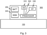
- Fig. 3 shows a schematic principle block view of a system according to a further example embodiment of the invention.
- the system comprises the apparatus 100 as hereinbefore described according to an example embodiment of the invention.
- the apparatus 100 is connected to a control element 300.
- the control element 300 comprises, or is comprised in, a separate device or comprises a separate element integrated with the apparatus 100.
- the control element 300 comprises electronics used with the apparatus 100.
- the control element 300 is connected to the apparatus 100 in a conventional manner, for example with wires or wirelessly with e.g. near field communication such as Bluetooth or Near Field Communication, NFC in which case the required communication components are provided on the apparatus 100 and the control element 300.
- near field communication such as Bluetooth or Near Field Communication, NFC
- the control element 300 comprises a memory 340, a battery 350 for powering the control element 300 and a processor 320.
- the processor 320 is configured to cause storing data from the apparatus 100 into the memory 340.
- the processor 320 is further configured to cause controlling of the operation of the apparatus 100 and the control element 300 itself using a non-transitory computer program code stored in the memory 340.
- the control element 300 comprises a communication unit 310 comprising, for example, a local area network (LAN) port; a wireless local area network (WLAN) unit; Bluetooth unit; cellular data communication unit; near field communication unit or satellite data communication unit.
- the control element 300 comprises a user interface unit 330.
- the processor 320 comprises, for example, any one or more of: a master control unit (MCU); a microprocessor; a digital signal processor (DSP); an application specific integrated circuit (ASIC); a field programmable gate array; and a microcontroller.
- the control element 300 comprises, or is comprised in, a personal electronic device such as a wristwatch, a smart watch, an activity bracelet, a mobile phone, a smartphone, a tablet, a computer or a television, configured to co-operate with the apparatus 100.
- Fig. 4 shows a flow chart of a method according to an example embodiment of the invention.
- electromagnetic radiation in an example embodiment visible light
- the light traverses the elastic element 20 and is randomly scattered therein by the optical elements 30 and/or the boundaries of the elastic element 20.
- the random scattering changes if force is applied to the elastic element 20 so that the elastic element 20 is deformed.
- the light having traversed the elastic element 20 and been scattered therein reaches the detector element 40 and is detected.
- the force applied to the elastic element is calculated from the detected light.
- the detected pattern of light detected by the detector element 40 when force is applied is compared to a previous pattern of light detected by the detector element 40 when no force or a different force has been applied to the elastic element 20 and a differential force is calculated therefrom.
- a small force applied to the elastic element 20 would change the paths of light traversing the elastic element 20 just a little for most of the light whereas a greater force would change the paths more.
- the calculation is carried out for example by comparing the values of each pixel of the imaging sensor with a previous values thereof and calculating a sum of differences yielding as result a modulus of time derivative of the deformation of the elastic element 20, i.e. modulus of first time derivative of force.
- the apparatus 100 is used to detect differential force in a health application for monitoring a sleeping person, for example an adult or even a small baby.
- the apparatus 100 is placed for example under a mattress in a bed with the elastic element 20 being formed as very thin elongated strip so as to be easily locatable under a mattress or bed linen and not to disturb the person sleeping thereon.
- the heartbeat, respiration and/or movements of the person are detected by the apparatus 100 combined with the control element 300 which is for example comprised in a personal electronic device.
- the apparatus 100 is integrated into an article of clothing or clothing accessory, for example sports clothing.
- the elastic element 20 is formed into a thin elongated strip or plate and integrated for example into pants legs to detect tension of muscles and the changes in force arising therefrom that deforms the elastic element 20. In such a case, also for example running cadence or further quantities are calculated from the changes in force.
- the apparatus 100 is integrated into a surface, for example a wall, floor, the surface of furniture or the surface of an electronic device in order to make the surface functional, i.e. to provide a surface that reacts to force being applied.
- the apparatus 100 with a thin elongated elastic element 20 follows the contours of the surface, for example under a coat of paint or canvas and detects any change in force being applied on the surface for example in order to activate a further device or action.
- a technical effect of one or more of the example embodiments disclosed herein is the provision of simple differential force sensor with straightforward production. Another technical effect of one or more of the example embodiments disclosed herein is the provision of a robust sensor, since even if the elastic material should get somewhat damaged, the sensor will still operate. Another technical effect of one or more of the example embodiments disclosed herein is a low cost differential force sensor due to the cheapness of the elastic material. A still further technical effect of one or more of the example embodiments disclosed herein is the provision of a differential force sensor requiring no calibration.
- Embodiments of the present invention may be implemented in software, hardware, application logic or a combination of software, hardware and application logic.
- the application logic, software or an instruction set is maintained on any one of various conventional computer-readable media.
- a "computer-readable medium" may be any media or means that can contain, store, communicate, propagate or transport the instructions for use by or in connection with an instruction execution system, apparatus, or device.
- a computer-readable medium may comprise a computer-readable storage medium that may be any media or means that can contain or store the instructions for use by or in connection with an instruction execution system, apparatus, or device, such as a computer.
- the different functions discussed herein may be performed in a different order and/or concurrently with each other. Furthermore, if desired, one or more of the before-described functions may be optional or may be combined.
Landscapes
- Physics & Mathematics (AREA)
- General Physics & Mathematics (AREA)
- Force Measurement Appropriate To Specific Purposes (AREA)
Abstract
Description
- The present application generally relates to force sensing. In particular, but not exclusively, the application relates to differential force sensing.
- This section illustrates useful background information without admission of any technique described herein representative of the state of the art.
- Force sensing is a technical field in which new applications of sensing technology require sensitive and robust force sensors at low cost, either for sensing absolute or differential force.
- There are optical force sensing solutions based on measuring deformation of an elastic structure. Such known solutions require a known structure and a careful placement of light source, light sensing elements and reflective structures or patterns in the elastic material. Furthermore, differential force sensing solutions exist. These are typically based on detecting changes of electrical characteristics caused by deformations of material, for example based on a change of capacitance of dielectric material or on piezoelectric effect.
- It is the objective of the invention to provide a differential force sensing solution that is robust, simple and has an easily adjustable sensitivity.
- Various aspects of examples of the invention are set out in the claims.
- According to a first example aspect of the present invention, there is provided an apparatus, comprising:
- an elastic element configured to deform as a force is applied thereto;
- at least one source element configured to transmit electromagnetic radiation into the elastic element; and
- at least one detector element configured to detect the electromagnetic radiation that has traversed the elastic element; wherein
- the elastic element comprises elastic material transparent to the electromagnetic radiation and optical elements embedded in the elastic transparent material; and wherein
- the optical elements are configured to scatter the electromagnetic radiation in such a way that the scattering is changed in response to the elastic element being deformed.
- The optical elements may comprise any of reflective elements, air bubbles, aluminium foil cutouts, plastic pellets with dimensions in millimeter range and/or malachite grinded and filtered to particles.
- The electromagnetic radiation may comprise visible light.
- The elastic material may comprise an elastic gel.
- The elastic element may have the from of an elongated thin strip.
- The at least one source element and the at least one detector element may be positioned at opposite ends of the elastic element.
- The at least one detector element may comprise an imaging sensor.
- The at least one source element may comprise a light emitting diode.
- According to a second example aspect of the present invention, there is provided a method comprising
transmitting electromagnetic radiation with at least one source element into an elastic element comprising elastic material transparent to the electromagnetic radiation and configured to deform as a force is applied thereto;
detecting with at least one detector element the electromagnetic radiation that has traversed the elastic element; and
calculating a change of force applied to the elastic element; wherein
the elastic element comprises optical elements embedded in the elastic transparent material; and wherein
the optical elements are configured to scatter the electromagnetic radiation in such a way that the scattering is changed in response to the elastic element being deformed. - According to a third example aspect of the present invention, there is provided a system comprising
a processor; and
the apparatus of the first example aspect of the present invention; wherein
the processor is configured to cause calculating a change of force applied to the elastic element - The system may further comprise a memory element and a communication element.
- According to a fourth example aspect of the present invention, there is provided a computer program comprising computer code for causing performing the method of the second example aspect of the present invention, when executed by an apparatus.
- According to a fifth example aspect of the present invention, there is provided a non-transitory memory medium comprising the computer program of the fourth example aspect of the present invention.
- Any memory medium hereinbefore or hereinafter may comprise a digital data storage such as a data disc or diskette, optical storage, magnetic storage, holographic storage, opto-magnetic storage, phase-change memory, resistive random access memory, magnetic random access memory, solid-electrolyte memory, ferroelectric random access memory, organic memory or polymer memory. The memory medium may be formed into a device without other substantial functions than storing memory or it may be formed as part of a device with other functions, including but not limited to a memory of a computer, a chip set, and a sub assembly of an electronic device. In the context of this document, a "memory medium" may be any non-transitory media or means that can contain, store, communicate, propagate or transport the instructions for use by or in connection with an instruction execution system, apparatus, or device, such as a computer.
- Different non-binding example aspects and embodiments of the present invention have been illustrated in the foregoing. The embodiments in the foregoing are used merely to explain selected aspects or steps that may be utilized in implementations of the present invention. Some embodiments may be presented only with reference to certain example aspects of the invention. It should be appreciated that corresponding embodiments may apply to other example aspects as well.
- For a more complete understanding of example embodiments of the present invention, reference is now made to the following descriptions taken in connection with the accompanying drawings in which:
-
Fig. 1A shows a schematic principle view of an apparatus according to an example embodiment of the invention; -
Fig. 1B shows a schematic principle view of an apparatus according to an example embodiment of the invention; -
Fig. 2A shows a schematic principle view of a detector element of an apparatus according to an example embodiment of the invention; -
Fig. 2B shows a schematic principle view of a detector element of an apparatus according to an example embodiment of the invention; -
Fig. 3 shows a schematic principle block view of an system according to a further example embodiment of the invention; and -
Fig. 4 shows a flow chart of a method according to an example embodiment of the invention. - An example embodiment of the present invention and its potential advantages are understood by referring to
Figs. 1 through 4 of the drawings. In this document, like reference signs denote like parts or steps. -
Figs. 1A and 1B show a schematic principle view of an apparatus according to an example embodiment of the invention. Theapparatus 100 is shown inFig. 1A in a situation in which no force is applied and inFig 1B in a situation in which force is applied. - The
apparatus 100 comprises at least onesource element 10 configured to transmit electromagnetic radiation. In an example embodiment, thesource element 10 comprises a light source and the electromagnetic radiation comprises light, for example visible or infrared light. In an example embodiment thesource element 10 comprises a light emitting diode, LED. In an example embodiment, the apparatus comprises a plurality ofsource elements 10, such as for example two source elements. - The
apparatus 100 further comprises anelastic element 20. Theelastic element 20 is configured to be deformed as a force F is applied thereto, as shown schematically inFig. 1B . In an example embodiment, the elastic element is in the form of an elongated strip, although other forms are also applicable. Theelastic element 20 comprises material that, in addition to being elastic, i.e. deformable, is transparent to the electromagnetic radiation transmitted into theelastic element 20 from thesource element 10. In an example embodiment, the material comprises transparent gel molded into a suitable form. In a further example embodiment, theelastic element 20 is not straight, but follows for example contours of a surface on which it is placed, i.e. the elastic element is in an embodiment curved or bent. - The
elastic element 20 further comprisesoptical elements 30 embedded, or placed, into the elastic transparent material. Theoptical elements 30 comprise, in an example embodiment, reflective elements, such as glitter. In a further example embodiment, theoptical elements 30 comprise in addition to or instead of the reflective elements further elements such as air bubbles, small aluminium foil cutouts with dimensions in millimeter range, plastic pellets with dimensions in millimeter range and/or malachite grinded and filtered to a particle size in the millimeter range. Theoptical elements 30 are configured to randomly scatter the electromagnetic radiation, for example light, transmitted into theelastic element 20 from thesource element 10. - A force F applied to the
elastic element 20 causes the elastic element to deform and the random scattering to change, since the alignment of the elastic element boundaries and/or of the optical elements is changed. A schematic example of a single light beam traversing theelastic element 20 without and with a force F being applied to theelastic element 20 is schematically shown inFigs. 1A and 1B with a dashed line. In reality, the light traversing the elastic element does not comprise a single beam as shown as an example inFigs. 1A and 1B but propagates as a wider beam through multiple routes. In an example embodiment, the surface of theelastic element 20 comprises at least on a part of the surface an opaque layer (not shown) configured to prevent or reduce ambient light from entering the elastic element. - The
apparatus 100 further comprises at least onedetector element 40. Thedetector element 40 is configured to receive and detect the electromagnetic radiation that has traversed theelastic element 20 and is incident on thedetector element 40. In an example embodiment, thedetector element 40 is located at the opposite end of theelastic element 20 from thesource element 10. In an example embodiment, thedetector element 40 comprises an imaging sensor, such as a CCD imaging sensor. In a further example embodiment, the detector element comprises a two dimensional array of photosensitive elements, a single strip, i.e. 1 dimensional array, of photosensitive elements, or a single photosensitive element. In a further example embodiment, the apparatus comprises a plurality ofdetector elements 40, for example two imaging sensors. In a still further example embodiment, the plurality ofdetector elements 40 and the plurality ofsource elements 10 are located in such a way that they reside on different positions around theelastic element 20, i.e. there aresource elements 10 and/ordetector elements 40 on several sides of theelastic element 20. -
Figs. 2A and 2B show schematic principle views of adetector element 40 of an apparatus according to an example embodiment of the invention. Thedetector element 40 is shown inFig. 2A in a situation in which no force is applied and inFig 2B in a situation in which force is applied, corresponding to the situations depicted inFigs. 1A and 1b as hereinbefore described.Figs. 2A and 2B show, with a cross, the position of an example beam on thedetector element 40. As force is applied to theelastic element 20, the pattern formed by the electromagnetic radiation having traversed theelastic element 20 on thedetector element 40 changes and accordingly the position of the example beam on the detector element changes, which change is detected and the change of the force applied to the elastic element is calculated from the detected change. -
Fig. 3 shows a schematic principle block view of a system according to a further example embodiment of the invention. The system comprises theapparatus 100 as hereinbefore described according to an example embodiment of the invention. Theapparatus 100 is connected to acontrol element 300. In an example embodiment, thecontrol element 300 comprises, or is comprised in, a separate device or comprises a separate element integrated with theapparatus 100. Thecontrol element 300 comprises electronics used with theapparatus 100. In an example embodiment, thecontrol element 300 is connected to theapparatus 100 in a conventional manner, for example with wires or wirelessly with e.g. near field communication such as Bluetooth or Near Field Communication, NFC in which case the required communication components are provided on theapparatus 100 and thecontrol element 300. - The
control element 300 comprises amemory 340, abattery 350 for powering thecontrol element 300 and aprocessor 320. Theprocessor 320 is configured to cause storing data from theapparatus 100 into thememory 340. Theprocessor 320 is further configured to cause controlling of the operation of theapparatus 100 and thecontrol element 300 itself using a non-transitory computer program code stored in thememory 340. In a further example embodiment, thecontrol element 300 comprises acommunication unit 310 comprising, for example, a local area network (LAN) port; a wireless local area network (WLAN) unit; Bluetooth unit; cellular data communication unit; near field communication unit or satellite data communication unit. In a further example embodiment thecontrol element 300 comprises auser interface unit 330. Theprocessor 320 comprises, for example, any one or more of: a master control unit (MCU); a microprocessor; a digital signal processor (DSP); an application specific integrated circuit (ASIC); a field programmable gate array; and a microcontroller. In a still further example embodiment, thecontrol element 300 comprises, or is comprised in, a personal electronic device such as a wristwatch, a smart watch, an activity bracelet, a mobile phone, a smartphone, a tablet, a computer or a television, configured to co-operate with theapparatus 100. -
Fig. 4 shows a flow chart of a method according to an example embodiment of the invention. Atstep 410 electromagnetic radiation, in an example embodiment visible light, is transmitted from thesource element 10 into theelastic element 20. Atstep 420, the light traverses theelastic element 20 and is randomly scattered therein by theoptical elements 30 and/or the boundaries of theelastic element 20. The random scattering changes if force is applied to theelastic element 20 so that theelastic element 20 is deformed. Atstep 430 the light having traversed theelastic element 20 and been scattered therein reaches thedetector element 40 and is detected. Atstep 440 the force applied to the elastic element is calculated from the detected light. In an example embodiment, the detected pattern of light detected by thedetector element 40 when force is applied is compared to a previous pattern of light detected by thedetector element 40 when no force or a different force has been applied to theelastic element 20 and a differential force is calculated therefrom. A small force applied to theelastic element 20 would change the paths of light traversing theelastic element 20 just a little for most of the light whereas a greater force would change the paths more. In an example embodiment, with an imaging sensor as thedetector element 40, the calculation is carried out for example by comparing the values of each pixel of the imaging sensor with a previous values thereof and calculating a sum of differences yielding as result a modulus of time derivative of the deformation of theelastic element 20, i.e. modulus of first time derivative of force. - Some use cases relating to given example embodiments of the differential force sensing are presented in the following. In a first use case, the
apparatus 100 is used to detect differential force in a health application for monitoring a sleeping person, for example an adult or even a small baby. Theapparatus 100 is placed for example under a mattress in a bed with theelastic element 20 being formed as very thin elongated strip so as to be easily locatable under a mattress or bed linen and not to disturb the person sleeping thereon. The heartbeat, respiration and/or movements of the person are detected by theapparatus 100 combined with thecontrol element 300 which is for example comprised in a personal electronic device. - In a second use case, the
apparatus 100 is integrated into an article of clothing or clothing accessory, for example sports clothing. Theelastic element 20 is formed into a thin elongated strip or plate and integrated for example into pants legs to detect tension of muscles and the changes in force arising therefrom that deforms theelastic element 20. In such a case, also for example running cadence or further quantities are calculated from the changes in force. - In a third use case, the
apparatus 100 is integrated into a surface, for example a wall, floor, the surface of furniture or the surface of an electronic device in order to make the surface functional, i.e. to provide a surface that reacts to force being applied. Theapparatus 100 with a thin elongatedelastic element 20 follows the contours of the surface, for example under a coat of paint or canvas and detects any change in force being applied on the surface for example in order to activate a further device or action. - Without in any way limiting the scope, interpretation, or application of the claims appearing below, a technical effect of one or more of the example embodiments disclosed herein is the provision of simple differential force sensor with straightforward production. Another technical effect of one or more of the example embodiments disclosed herein is the provision of a robust sensor, since even if the elastic material should get somewhat damaged, the sensor will still operate. Another technical effect of one or more of the example embodiments disclosed herein is a low cost differential force sensor due to the cheapness of the elastic material. A still further technical effect of one or more of the example embodiments disclosed herein is the provision of a differential force sensor requiring no calibration.
- Embodiments of the present invention may be implemented in software, hardware, application logic or a combination of software, hardware and application logic. In an example embodiment, the application logic, software or an instruction set is maintained on any one of various conventional computer-readable media. In the context of this document, a "computer-readable medium" may be any media or means that can contain, store, communicate, propagate or transport the instructions for use by or in connection with an instruction execution system, apparatus, or device. A computer-readable medium may comprise a computer-readable storage medium that may be any media or means that can contain or store the instructions for use by or in connection with an instruction execution system, apparatus, or device, such as a computer.
- If desired, the different functions discussed herein may be performed in a different order and/or concurrently with each other. Furthermore, if desired, one or more of the before-described functions may be optional or may be combined.
- Although various aspects of the invention are set out in the independent claims, other aspects of the invention comprise other combinations of features from the described embodiments and/or the dependent claims with the features of the independent claims, and not solely the combinations explicitly set out in the claims.
- It is also noted herein that while the foregoing describes example embodiments of the invention, these descriptions should not be viewed in a limiting sense. Rather, there are several variations and modifications which may be made without departing from the scope of the present invention as defined in the appended claims.
Claims (13)
- An apparatus, comprising:an elastic element configured to deform as a force is applied thereto;at least one source element configured to transmit electromagnetic radiation into the elastic element; andat least one detector element configured to detect the electromagnetic radiation that has traversed the elastic element; whereinthe elastic element comprises elastic material transparent to the electromagnetic radiation and optical elements embedded in the elastic transparent material; and whereinthe optical elements are configured to scatter the electromagnetic radiation in such a way that the scattering is changed in response to the elastic element being deformed.
- The apparatus of claim 1, wherein the optical elements comprise any one or more optical elements selected from a group consisting of: reflective elements, air bubbles, aluminium foil cutouts, plastic pellets with dimensions in millimeter range, and malachite grinded and filtered to particles.
- The apparatus of claim 1 or 2, wherein the electromagnetic radiation comprises visible light.
- The apparatus of any preceding claim, wherein the elastic material comprises an elastic gel.
- The apparatus of any preceding claim, wherein the elastic element has the from of an elongated thin strip.
- The apparatus of any preceding claim, wherein the at least one source element and the at least one detector element are positioned at opposite ends of the elastic element.
- The apparatus of any preceding claim, wherein the at least one detector element comprises an imaging sensor.
- The apparatus of any preceding claim, wherein the at least one source element comprises a light emitting diode.
- A Method comprisingtransmitting electromagnetic radiation with at least one source element into an elastic element comprising elastic material transparent to the electromagnetic radiation and configured to deform as a force is applied thereto;detecting with at least one detector element the electromagnetic radiation that has traversed the elastic element; andcalculating a change of force applied to the elastic element; whereinthe elastic element comprises optical elements embedded in the elastic transparent material; and whereinthe optical elements are configured to scatter the electromagnetic radiation in such a way that the scattering is changed in response to the elastic element being deformed.
- A system comprisinga processor; andthe apparatus of any of the claims 1 to 8; whereinthe processor is configured to cause calculating a change of force applied to the elastic element
- The system of claim 10, further comprising a memory element and a communication element.
- A computer program comprising computer code for causing performing the method of claim 9, when executed by an apparatus.
- A non-transitory memory medium comprising the computer program of claim 12.
Priority Applications (1)
| Application Number | Priority Date | Filing Date | Title |
|---|---|---|---|
| EP16199920.6A EP3324166A1 (en) | 2016-11-22 | 2016-11-22 | Force sensing |
Applications Claiming Priority (1)
| Application Number | Priority Date | Filing Date | Title |
|---|---|---|---|
| EP16199920.6A EP3324166A1 (en) | 2016-11-22 | 2016-11-22 | Force sensing |
Publications (1)
| Publication Number | Publication Date |
|---|---|
| EP3324166A1 true EP3324166A1 (en) | 2018-05-23 |
Family
ID=57538994
Family Applications (1)
| Application Number | Title | Priority Date | Filing Date |
|---|---|---|---|
| EP16199920.6A Withdrawn EP3324166A1 (en) | 2016-11-22 | 2016-11-22 | Force sensing |
Country Status (1)
| Country | Link |
|---|---|
| EP (1) | EP3324166A1 (en) |
Cited By (1)
| Publication number | Priority date | Publication date | Assignee | Title |
|---|---|---|---|---|
| US11885700B2 (en) * | 2020-08-28 | 2024-01-30 | Samsung Electronics Co., Ltd. | Stretchable strain sensor, combination sensor, and display panel and device |
Citations (8)
| Publication number | Priority date | Publication date | Assignee | Title |
|---|---|---|---|---|
| JP2002318354A (en) * | 2001-04-23 | 2002-10-31 | Hamamatsu Photonics Kk | Light waveform shaping device |
| WO2005012885A1 (en) * | 2003-07-31 | 2005-02-10 | Stiftung Caesar Center Of Advanced Studies And Research | Non-contact optical extension sensor for measuring modifications in the particle plasmon resonance |
| WO2005029028A1 (en) * | 2003-09-16 | 2005-03-31 | Toudai Tlo, Ltd. | Optical tactile sensor and method of reconstructing force vector distribution using the sensor |
| WO2005085766A2 (en) * | 2004-03-01 | 2005-09-15 | University Of Washington Techtransfer Invention Licensing | Polymer based distributive waveguide sensor for pressure and shear measurement |
| JP2006242819A (en) * | 2005-03-04 | 2006-09-14 | National Institute For Materials Science | Method and apparatus for detecting distortion of an object |
| US20120250001A1 (en) * | 2009-11-27 | 2012-10-04 | National University Corporation Kyoto Institute Of Technology | Stress measurement device and stress measurement method |
| US20140182391A1 (en) * | 2012-12-28 | 2014-07-03 | National Chiao Tung University | Pressure and shear force measurement device and method |
| WO2017025616A1 (en) * | 2015-08-13 | 2017-02-16 | Museum National D'histoire Naturelle | Force sensor |
-
2016
- 2016-11-22 EP EP16199920.6A patent/EP3324166A1/en not_active Withdrawn
Patent Citations (8)
| Publication number | Priority date | Publication date | Assignee | Title |
|---|---|---|---|---|
| JP2002318354A (en) * | 2001-04-23 | 2002-10-31 | Hamamatsu Photonics Kk | Light waveform shaping device |
| WO2005012885A1 (en) * | 2003-07-31 | 2005-02-10 | Stiftung Caesar Center Of Advanced Studies And Research | Non-contact optical extension sensor for measuring modifications in the particle plasmon resonance |
| WO2005029028A1 (en) * | 2003-09-16 | 2005-03-31 | Toudai Tlo, Ltd. | Optical tactile sensor and method of reconstructing force vector distribution using the sensor |
| WO2005085766A2 (en) * | 2004-03-01 | 2005-09-15 | University Of Washington Techtransfer Invention Licensing | Polymer based distributive waveguide sensor for pressure and shear measurement |
| JP2006242819A (en) * | 2005-03-04 | 2006-09-14 | National Institute For Materials Science | Method and apparatus for detecting distortion of an object |
| US20120250001A1 (en) * | 2009-11-27 | 2012-10-04 | National University Corporation Kyoto Institute Of Technology | Stress measurement device and stress measurement method |
| US20140182391A1 (en) * | 2012-12-28 | 2014-07-03 | National Chiao Tung University | Pressure and shear force measurement device and method |
| WO2017025616A1 (en) * | 2015-08-13 | 2017-02-16 | Museum National D'histoire Naturelle | Force sensor |
Cited By (2)
| Publication number | Priority date | Publication date | Assignee | Title |
|---|---|---|---|---|
| US11885700B2 (en) * | 2020-08-28 | 2024-01-30 | Samsung Electronics Co., Ltd. | Stretchable strain sensor, combination sensor, and display panel and device |
| US12313481B2 (en) | 2020-08-28 | 2025-05-27 | Samsung Electronics Co., Ltd. | Stretchable strain sensor, combination sensor, and display panel and device |
Similar Documents
| Publication | Publication Date | Title |
|---|---|---|
| KR102446849B1 (en) | Electronic device and method for identifying forgery of biometric information | |
| US10051347B2 (en) | Displacement sensor | |
| KR102419624B1 (en) | Arrangement structure of sensor of electronic apparatus | |
| JP6039072B2 (en) | Method, storage medium and apparatus for mobile device state adjustment based on user intent and / or identification information | |
| CN112101080B (en) | Identification system using thermal sensors | |
| KR102786948B1 (en) | Proximity sensing apparatus in electronic device and method thereof | |
| US20180240323A1 (en) | Sensor configuration | |
| EP2634553A1 (en) | Temperature sensing device | |
| US9153114B2 (en) | Fall detection method and system | |
| KR102688107B1 (en) | Spectrometric sensing apparatus in electronic device and method thereof | |
| CN105828705B (en) | Skin Proximity and Tilt Effect Sensors | |
| EP3721387A1 (en) | Automated localized machine learning training | |
| KR20180031028A (en) | Transparent strain sensors in electronic devices | |
| KR102400840B1 (en) | Method for obtaining biometric information using a display as a light source and electronic device thereof | |
| CN107530000A (en) | Dynamically configurable aperture for ppg signal optimization and ambient light mitigation | |
| ES2729245T3 (en) | Virtual button based on ultrasonic touch sensor | |
| US11852523B2 (en) | Optical sensor having directional sensitivity | |
| FR2852400B1 (en) | MAGNETORESISTIVE SENSOR COMPRISING A SENSITIVE FERROMAGNETIC / ANTIFERROMAGNETIC ELEMENT | |
| TWI736552B (en) | Electronic device with night function and method thereof | |
| KR102373457B1 (en) | Electronic device and method for controlling sensitivity of a sensor based on properties of window in electronic device | |
| CN107250956B (en) | Method and system for dual node sensing | |
| CN111265197A (en) | Electronic device and method for wearable electronic device | |
| EP3894985C0 (en) | DISPLAY MODULE COMPRISING A SENSOR AND ELECTRONIC DEVICE INCLUDING SAME | |
| KR102178558B1 (en) | Apparatus and method for sensing touch | |
| CN104391597B (en) | A kind of pressure detection method and equipment |
Legal Events
| Date | Code | Title | Description |
|---|---|---|---|
| PUAI | Public reference made under article 153(3) epc to a published international application that has entered the european phase |
Free format text: ORIGINAL CODE: 0009012 |
|
| STAA | Information on the status of an ep patent application or granted ep patent |
Free format text: STATUS: THE APPLICATION HAS BEEN PUBLISHED |
|
| AK | Designated contracting states |
Kind code of ref document: A1 Designated state(s): AL AT BE BG CH CY CZ DE DK EE ES FI FR GB GR HR HU IE IS IT LI LT LU LV MC MK MT NL NO PL PT RO RS SE SI SK SM TR |
|
| AX | Request for extension of the european patent |
Extension state: BA ME |
|
| STAA | Information on the status of an ep patent application or granted ep patent |
Free format text: STATUS: REQUEST FOR EXAMINATION WAS MADE |
|
| 17P | Request for examination filed |
Effective date: 20181122 |
|
| RBV | Designated contracting states (corrected) |
Designated state(s): AL AT BE BG CH CY CZ DE DK EE ES FI FR GB GR HR HU IE IS IT LI LT LU LV MC MK MT NL NO PL PT RO RS SE SI SK SM TR |
|
| STAA | Information on the status of an ep patent application or granted ep patent |
Free format text: STATUS: EXAMINATION IS IN PROGRESS |
|
| 17Q | First examination report despatched |
Effective date: 20190408 |
|
| RAP1 | Party data changed (applicant data changed or rights of an application transferred) |
Owner name: PROVENANCE ASSET GROUP LLC |
|
| STAA | Information on the status of an ep patent application or granted ep patent |
Free format text: STATUS: THE APPLICATION IS DEEMED TO BE WITHDRAWN |
|
| 18D | Application deemed to be withdrawn |
Effective date: 20190820 |