EP3322265A1 - Production method for wiring circuit board - Google Patents
Production method for wiring circuit board Download PDFInfo
- Publication number
- EP3322265A1 EP3322265A1 EP16821123.3A EP16821123A EP3322265A1 EP 3322265 A1 EP3322265 A1 EP 3322265A1 EP 16821123 A EP16821123 A EP 16821123A EP 3322265 A1 EP3322265 A1 EP 3322265A1
- Authority
- EP
- European Patent Office
- Prior art keywords
- circuit board
- insulating layer
- resin
- layer
- conductive pattern
- Prior art date
- Legal status (The legal status is an assumption and is not a legal conclusion. Google has not performed a legal analysis and makes no representation as to the accuracy of the status listed.)
- Granted
Links
Images

Classifications
-
- H—ELECTRICITY
- H05—ELECTRIC TECHNIQUES NOT OTHERWISE PROVIDED FOR
- H05K—PRINTED CIRCUITS; CASINGS OR CONSTRUCTIONAL DETAILS OF ELECTRIC APPARATUS; MANUFACTURE OF ASSEMBLAGES OF ELECTRICAL COMPONENTS
- H05K3/00—Apparatus or processes for manufacturing printed circuits
- H05K3/10—Apparatus or processes for manufacturing printed circuits in which conductive material is applied to the insulating support in such a manner as to form the desired conductive pattern
- H05K3/20—Apparatus or processes for manufacturing printed circuits in which conductive material is applied to the insulating support in such a manner as to form the desired conductive pattern by affixing prefabricated conductor pattern
-
- H—ELECTRICITY
- H05—ELECTRIC TECHNIQUES NOT OTHERWISE PROVIDED FOR
- H05K—PRINTED CIRCUITS; CASINGS OR CONSTRUCTIONAL DETAILS OF ELECTRIC APPARATUS; MANUFACTURE OF ASSEMBLAGES OF ELECTRICAL COMPONENTS
- H05K1/00—Printed circuits
- H05K1/02—Details
- H05K1/0277—Bendability or stretchability details
- H05K1/0283—Stretchable printed circuits
-
- H—ELECTRICITY
- H05—ELECTRIC TECHNIQUES NOT OTHERWISE PROVIDED FOR
- H05K—PRINTED CIRCUITS; CASINGS OR CONSTRUCTIONAL DETAILS OF ELECTRIC APPARATUS; MANUFACTURE OF ASSEMBLAGES OF ELECTRICAL COMPONENTS
- H05K3/00—Apparatus or processes for manufacturing printed circuits
- H05K3/007—Manufacture or processing of a substrate for a printed circuit board supported by a temporary or sacrificial carrier
-
- H—ELECTRICITY
- H05—ELECTRIC TECHNIQUES NOT OTHERWISE PROVIDED FOR
- H05K—PRINTED CIRCUITS; CASINGS OR CONSTRUCTIONAL DETAILS OF ELECTRIC APPARATUS; MANUFACTURE OF ASSEMBLAGES OF ELECTRICAL COMPONENTS
- H05K3/00—Apparatus or processes for manufacturing printed circuits
- H05K3/22—Secondary treatment of printed circuits
-
- H—ELECTRICITY
- H05—ELECTRIC TECHNIQUES NOT OTHERWISE PROVIDED FOR
- H05K—PRINTED CIRCUITS; CASINGS OR CONSTRUCTIONAL DETAILS OF ELECTRIC APPARATUS; MANUFACTURE OF ASSEMBLAGES OF ELECTRICAL COMPONENTS
- H05K2201/00—Indexing scheme relating to printed circuits covered by H05K1/00
- H05K2201/01—Dielectrics
- H05K2201/0104—Properties and characteristics in general
- H05K2201/0133—Elastomeric or compliant polymer
-
- H—ELECTRICITY
- H05—ELECTRIC TECHNIQUES NOT OTHERWISE PROVIDED FOR
- H05K—PRINTED CIRCUITS; CASINGS OR CONSTRUCTIONAL DETAILS OF ELECTRIC APPARATUS; MANUFACTURE OF ASSEMBLAGES OF ELECTRICAL COMPONENTS
- H05K2201/00—Indexing scheme relating to printed circuits covered by H05K1/00
- H05K2201/01—Dielectrics
- H05K2201/0137—Materials
- H05K2201/0158—Polyalkene or polyolefin, e.g. polyethylene [PE], polypropylene [PP]
-
- H—ELECTRICITY
- H05—ELECTRIC TECHNIQUES NOT OTHERWISE PROVIDED FOR
- H05K—PRINTED CIRCUITS; CASINGS OR CONSTRUCTIONAL DETAILS OF ELECTRIC APPARATUS; MANUFACTURE OF ASSEMBLAGES OF ELECTRICAL COMPONENTS
- H05K2201/00—Indexing scheme relating to printed circuits covered by H05K1/00
- H05K2201/03—Conductive materials
- H05K2201/0332—Structure of the conductor
- H05K2201/0364—Conductor shape
- H05K2201/0376—Flush conductors, i.e. flush with the surface of the printed circuit
-
- H—ELECTRICITY
- H05—ELECTRIC TECHNIQUES NOT OTHERWISE PROVIDED FOR
- H05K—PRINTED CIRCUITS; CASINGS OR CONSTRUCTIONAL DETAILS OF ELECTRIC APPARATUS; MANUFACTURE OF ASSEMBLAGES OF ELECTRICAL COMPONENTS
- H05K2201/00—Indexing scheme relating to printed circuits covered by H05K1/00
- H05K2201/05—Flexible printed circuits [FPCs]
- H05K2201/051—Rolled
-
- H—ELECTRICITY
- H05—ELECTRIC TECHNIQUES NOT OTHERWISE PROVIDED FOR
- H05K—PRINTED CIRCUITS; CASINGS OR CONSTRUCTIONAL DETAILS OF ELECTRIC APPARATUS; MANUFACTURE OF ASSEMBLAGES OF ELECTRICAL COMPONENTS
- H05K3/00—Apparatus or processes for manufacturing printed circuits
- H05K3/10—Apparatus or processes for manufacturing printed circuits in which conductive material is applied to the insulating support in such a manner as to form the desired conductive pattern
- H05K3/108—Apparatus or processes for manufacturing printed circuits in which conductive material is applied to the insulating support in such a manner as to form the desired conductive pattern by semi-additive methods; masks therefor
-
- Y—GENERAL TAGGING OF NEW TECHNOLOGICAL DEVELOPMENTS; GENERAL TAGGING OF CROSS-SECTIONAL TECHNOLOGIES SPANNING OVER SEVERAL SECTIONS OF THE IPC; TECHNICAL SUBJECTS COVERED BY FORMER USPC CROSS-REFERENCE ART COLLECTIONS [XRACs] AND DIGESTS
- Y10—TECHNICAL SUBJECTS COVERED BY FORMER USPC
- Y10T—TECHNICAL SUBJECTS COVERED BY FORMER US CLASSIFICATION
- Y10T29/00—Metal working
- Y10T29/49—Method of mechanical manufacture
- Y10T29/49002—Electrical device making
- Y10T29/49117—Conductor or circuit manufacturing
- Y10T29/49124—On flat or curved insulated base, e.g., printed circuit, etc.
- Y10T29/49155—Manufacturing circuit on or in base
Definitions
- the present invention relates to a method for producing a wired circuit board.
- a wired circuit board such as printed wiring board is produced by various producing methods.
- a method for producing a printed wiring board has been proposed in which a metal film is provided on the surface of a metal material and a transfer circuit is provided on the surface of the metal film, so that a transfer substrate is produced; the transfer substrate is attached to a resin layer to embed the transfer circuit into the resin layer; and thereafter, the metal material is peeled and the metal film is removed by etching (ref: for example, Patent Document 1).
- a prepreg that is formed by impregnating a thermosetting resin such as epoxy resin in a substrate such as glass fabric to be dried by heating until being brought into a B-stage state and an adhesive sheet such as adhesive film that is formed by molding a thermosetting resin such as epoxy resin into a film shape to be dried by heating until being brought into a B-stage state are used.
- Patent Document 1 Japanese Unexamined Patent Publication No. 2010-80568
- An object of the present invention is to provide a method for producing a wired circuit board having excellent elastic properties.
- the present invention [1] includes a method for producing a wired circuit board including a step (1) of forming a seed layer on one surface in a thickness direction of a peeling layer, a step (2) of forming a conductive pattern on one surface in the thickness direction of the seed layer, a step (3) of covering the seed layer and the conductive pattern with an insulating layer, a step (4) of peeling the peeling layer from the seed layer, and a step (5) of removing the seed layer, wherein the insulating layer has the number of times of folding endurance measured in conformity with JIS P8115 (2001) of 10 times or more.
- the insulating layer has the number of times of folding endurance measured in conformity with JIS P8115 (2001) of the above-described lower limit or more, so that the wired circuit board has excellent elastic properties.
- the present invention [2] includes the method for producing a wired circuit board described in the above-described [1], wherein the insulating layer is formed of at least one kind of insulating material selected from the group consisting of polyurethane resin, (meth)acrylic resin, urethane-(meth)acrylic resin, silicone resin, polyolefin resin, polyvinyl chloride resin, polyvinylidene chloride resin, polyvinyl acetate resin, fluorine resin, styrene resin, butadiene resin, and isobutylene resin.
- polyurethane resin polyurethane resin
- (meth)acrylic resin urethane-(meth)acrylic resin
- silicone resin polyolefin resin
- polyvinyl chloride resin polyvinylidene chloride resin
- polyvinyl acetate resin polyvinyl acetate resin
- fluorine resin styrene resin
- butadiene resin butadiene resin
- the insulating layer can have both flexibility and toughness.
- the wired circuit board has excellent elastic properties and excellent reliability.
- the wired circuit board of the present invention has excellent elastic properties.
- the right-left direction of the paper surface is a right-left direction (first direction)
- the left side of the paper surface is a left side (one side in the first direction)
- the right side of the paper surface is a right side (the other side in the first direction).
- the up-down direction of the paper surface is an up-down direction (second direction perpendicular to the first direction, thickness direction)
- the upper side of the paper surface is an upper side (one side in the second direction, one side in the thickness direction)
- the lower side of the paper surface is a lower side (the other side in the second direction, the other side in the thickness direction).
- the depth direction of the paper surface is a front-rear direction (third direction perpendicular to the first direction and the second direction, longitudinal direction (ref: FIG. 1 )), the near side of the paper surface is a front side (one side in the third direction, one side in the longitudinal direction), and the far side of the paper surface is a rear side (the other side in the third direction, the other side in the longitudinal direction).
- the directions are in conformity with the direction arrows in each figure.
- FIGS. 4A to 4C a sensor 18 and a memory 25 (described later) are omitted so as to clearly show the shape of a wired circuit board 1 (described later).
- the wired circuit board 1 that is one embodiment of the present invention includes an insulating layer 2 and conductive patterns 3 that are embedded in the insulating layer 2.
- the insulating layer 2 has the same outer shape as that of the wired circuit board 1.
- the insulating layer 2 has a film (sheet) shape in a generally rectangular shape when viewed from the top extending in the front-rear direction.
- the insulating layer 2 includes a flat lower surface 10 and an upper surface 11 facing the upper side of the lower surface 10 at spaced intervals thereto.
- the insulating layer 2 includes a plurality of ditch portions 4 corresponding to the conductive patterns 3. Each of the plurality of ditch portions 4 has an opening upwardly.
- the insulating layer 2 is, for example, formed of an insulating material that satisfies the number of times of folding endurance to be described later.
- the insulating material include polyurethane resin, (meth)acrylic resin (meaning acrylic resin and/or methacrylic resin, hereinafter, the same), urethane-(meth)acrylic resin, silicone resin, polyolefin resin (to be specific, polyethylene resin, polypropylene resin, or the like), polyvinyl chloride resin, polyvinylidene chloride resin, polyvinyl acetate resin, fluorine resin, styrene resin, butadiene resin, and isobutylene resin.
- the insulating materials can be used alone or in combination of two or more.
- the insulating material in order to obtain characteristics of having both flexibility and toughness, preferably, polyurethane resin, (meth)acrylic resin, urethane-(meth)acrylic resin, and silicone resin are used, and in view of obtaining excellent folding endurance, more preferably, urethane-(meth)acrylic resin and silicone resin are used.
- the urethane-(meth)acrylic resin is an ultraviolet curing resin, and is, for example, obtained by blending a material containing polyol, polyisocyanate, (meth)acrylic acid, and (meth)acrylate to be allowed to react under the presence of a photopolymerization initiator.
- a material containing polyol, polyisocyanate, (meth)acrylic acid, and (meth)acrylate to be allowed to react under the presence of a photopolymerization initiator.
- the above-described material and the above-described photopolymerization initiator are blended to prepare a mixture, and an ultraviolet ray is applied to the mixture to cure.
- the silicone resin is a thermosetting resin, and examples thereof include polydimethyl siloxane, polymethylphenyl siloxane, and polydiphenyl siloxane. Preferably, polydimethyl siloxane is used.
- the insulating layer 2 has the number of times of folding endurance measured in conformity with JIS P8115 (2001) of 10 times or more, preferably 100 times or more, more preferably, 1000 times or more, further more preferably, 10000 times or more and, for example, 100000 times or less.
- the number of times of folding endurance of the insulating layer 2 is below the above-described lower limit, the peeling of the conductive pattern 3 from the insulating layer 2 cannot be suppressed at the time of repeatedly expanding or contracting the wired circuit board 1.
- a tensile storage elastic modulus E' at 20°C of the insulating layer 2 is, for example, 2000 MPa or less, preferably 1000 MPa or less, more preferably 100 MPa or less, further more preferably 50 MPa or less, particularly preferably 20 MPa or less, and for example, 0.1 MPa or more, preferably 0.5 MPa or more.
- the tensile storage elastic modulus E' of the insulating layer 2 is the above-described upper limit or less, excellent elastic properties of the insulating layer 2 can be ensured. Meanwhile, when the tensile storage elastic modulus E' of the insulating layer 2 is the above-described lower limit or more, excellent toughness and excellent handleability can be ensured.
- the tensile storage elastic modulus E' at 20°C of the insulating layer 2 is obtained by subjecting the insulating layer 2 to dynamic viscoelasticity measurement under the conditions of a frequency of 1 Hz and a temperature rising rate of 10°C/min.
- a thickness T0 of the insulating layer 2 is, for example, 5 ⁇ m or more, preferably 10 ⁇ m or more, and for example, 1000 ⁇ m or less, preferably 300 ⁇ m or less.
- the thickness T0 of the insulating layer 2 is a distance T0 in the thickness direction between the lower surface 10 and the upper surface 11 of the insulating layer 2 in a region that is not overlapped with the conductive patterns 3 when projected in the thickness direction.
- the thickness T0 of the insulating layer 2 is the same as the thickness of the wired circuit board 1.
- the conductive patterns 3 are disposed so as to be included in a projected surface of the insulating layer 2 when projected in the thickness direction.
- the conductive patterns 3 integrally include wires 5 extending in the front-rear direction and terminals 6 that are connected to both end portions in the front-rear direction of the wires 5.
- the plurality of wires 5 are provided at spaced intervals to each other in the right-left direction.
- Each of the plurality of wires 5 has a generally wave shape (or sine wave shape).
- the plurality of terminals 6 are provided in the front end portion and the rear end portion of the wired circuit board 1. Each of the plurality of terminals 6 is provided so as to be continuous to both end portions in the front-rear direction of the wires 5. Each of the plurality of terminals 6 is a land having a generally rectangular shape when viewed from the top.
- the conductive pattern 3 (to be specific, the wire 5) has a generally rectangular shape when viewed in cross section.
- the conductive pattern 3 integrally has, as one example of an exposed surface, an upper surface 7, as one example of a facing surface, a lower surface 8 that is disposed at the lower side (one example of the other side in the thickness direction) facing the upper surface 7 at spaced intervals thereto, and as one example of a connecting surface, side surfaces 9 that connect the periphery end portion of the upper surface 7 to the periphery end portion of the lower surface 8.
- the conductive patterns 3 fit in the ditch portions 4 so as to be exposed from the upper surface 11 of the insulating layer 2.
- the upper surface 7 of the conductive pattern 3 is positioned at the lower side (one example of the other side in the thickness direction) with respect to the upper surface 11 of the insulating layer 2.
- a step portion 21 with respect to the upper surface 11 of the insulating layer 2 is formed by the upper surface 7 of the conductive pattern 3 and the inner-side surfaces of the ditch portion 4 that are at the upper side with respect to the upper surface 7.
- the upper surface 7 of the conductive pattern 3 is a surface that is in parallel with the upper surface 11 of the insulating layer 2, and a flat surface extending in the front-rear direction. Furthermore, the upper surface 7 of the conductive pattern 3 is an exposed surface that is exposed from the upper surface 11 of the insulating layer 2.
- the lower surface 8 of the conductive pattern 3 is a flat surface that is in parallel with the upper surface 7 of the conductive pattern 3.
- the lower surface 8 of the conductive pattern 3 is covered with the inner-side surfaces of the ditch portion 4 of the insulating layer 2.
- the lower surface 8 of the conductive pattern 3 is in direct contact with the ditch portion 4 of the insulating layer 2.
- the side surfaces 9 of the conductive pattern 3 are surfaces along the thickness direction (the up-down direction), and are covered with the inner-side surfaces of the ditch portion 4 of the insulating layer 2.
- the side surfaces 9 of the conductive pattern 3 are in direct contact with the ditch portion 4 of the insulating layer 2.
- the conductive pattern 3 is, for example, formed of a conductive material such as copper, nickel, and gold or an alloy thereof.
- a conductive material such as copper, nickel, and gold or an alloy thereof.
- copper is used as the conductive material.
- the size of the conductive pattern 3 is appropriately set in accordance with its usages and purpose, and is not particularly limited.
- a length (width) in the right-left direction of each of the plurality of wires 5 is for example, 12 ⁇ m or more, preferably 15 ⁇ m or more, and for example, 1000 ⁇ m or less, preferably 750 ⁇ m or less.
- An interval between the wires 5 that are next to each other is, for example, 12 ⁇ m or more, preferably 15 ⁇ m or more, and for example, 10000 ⁇ m or less, preferably 7500 ⁇ m or less.
- a length (width) in the front-rear direction of each of the plurality of wires 5 is, for example, 10 mm or more, preferably 20 mm or more, and for example, 250 mm or less, preferably 100 mm or less.
- a length in the right-left direction and a length in the front-rear direction of each of the plurality of terminals 6 are, for example, 100 ⁇ m or more, preferably 200 ⁇ m or more, and for example, 10000 ⁇ m or less, preferably 5000 ⁇ m or less.
- An interval between the terminals 6 that are next to each other is, for example, 50 ⁇ m or more, preferably 100 ⁇ m or more, and for example, 10000 ⁇ m or less, preferably 5000 ⁇ m or less.
- the ratio (S1/S0) of a plane area S1 (projected area when projected in the thickness direction) of the conductive pattern 3 to a plane area S0 of the insulating layer 2, that is, the ratio of the conductive pattern 3 to the insulating layer 2 when projected in the thickness direction is, for example, 70% or less, preferably 60% or less, and for example, 1% or more, preferably 3% or more.
- the ratio of S1/S0 is the above-described upper limit or less, the wired circuit board 1 has excellent elastic properties.
- a thickness T1 (distance T1 in the thickness direction between the upper surface 7 and the lower surface 8) of the conductive pattern 3, that is, the thickness T1 of each of the wires 5 and the terminals 6 is, for example, 0.3 ⁇ m or more, preferably 0.8 ⁇ m or more, more preferably 1.0 ⁇ m or more, and for example, 112 ⁇ m or less, preferably 75 ⁇ m or less, more preferably 40 ⁇ m or less.
- the thickness T1 of the conductive pattern 3 is the above-described lower limit or more, an adhesive force of the conductive pattern 3 with respect to the insulating layer 2 can be improved, and the peeling of the conductive pattern 3 from the insulating layer 2 can be suppressed.
- the ratio (T1/T0) of the thickness T1 of the conductive pattern 3 to the thickness T0 of the insulating layer 2 is, for example, below 1, preferably 0.9 or less, more preferably 0.8 or less, and for example, 0.05 or more, preferably 0.1 or more, more preferably 0.2 or more.
- the ratio of T1/T0 is the above-described lower limit or more, thinning of the wired circuit board 1 can be achieved.
- a thickness T2 of the insulating layer 2 that is positioned at the lower side of the conductive pattern 3, that is, the thickness T2 of the insulating layer 2 facing the conductive pattern 3 in the thickness direction is, for example, 200 ⁇ m or less, preferably 150 ⁇ m or less, more preferably 10 ⁇ m or less, and for example, 5 ⁇ m or more.
- the ratio (T2/T0) of the thickness T2 of the insulating layer 2 that is positioned at the lower side of the conductive pattern 3 to the thickness T0 of the insulating layer 2 is, for example, 0.95 or less, preferably 0.85 or less, more preferably 0.75 or less, and for example, 0.1 or more.
- the ratio of T2/T0 is the above-described upper limit or less, thinning of the wired circuit board 1 can be achieved, while an adhesive force of the conductive pattern 3 with respect to the insulating layer 2 is ensured.
- the ratio (T1/T2) of the thickness T1 of the conductive pattern 3 to the thickness T2 of the insulating layer 2 that is positioned at the lower side of the conductive pattern 3 is, for example, 0.05 or more, preferably 0.1 or more, and for example, 0.9 or less, preferably 0.8 or less.
- the ratio of T1/T2 is the above-described lower limit or more, thinning of the wired circuit board 1 can be achieved.
- a distance T6 in the thickness direction between the upper surface 7 of the conductive pattern 3 and the upper surface 11 of the insulating layer 2, that is, a depth T6 of the above-described step portion 21 is, for example, 0.5 ⁇ m or more, preferably 1 ⁇ m or more, and for example, 10 ⁇ m or less, preferably 5 ⁇ m or less.
- the ratio (T6/T0) of the depth T6 of the step portion 21 to the thickness T0 of the insulating layer 2 is, for example, 0.01 or more, preferably 0.03 or more, and for example, 0.5 or less, preferably 0.3 or less.
- the ratio of T6/T0 is the above-described lower limit or more, the time to remove a seed layer 15 in a step (5) to be described later can be sufficiently ensured, so that a short circuit of the conductive patterns 3 that are next to each other via the seed layer 15 can be suppressed.
- the sum (T1 + T6) of the thickness T1 of the conductive pattern 3 and the depth T6 of the step portion 21 is a depth of the ditch portion 4, and is, for example, 1 ⁇ m or more, preferably 10 ⁇ m or more, and for example, 300 ⁇ m or less, preferably 100 ⁇ m or less.
- the ratio ((T1 + T6)/T0) of the depth (T1 + T6) of the ditch portion 4 to the thickness T0 of the insulating layer 2 is, for example, 0.1 or more, preferably 0.2 or more, and for example, 0.9 or less, preferably 0.8 or less.
- the above-described ratio is the above-described lower limit or more, thinning of the wired circuit board 1 can be achieved, while an adhesive force of the conductive pattern 3 with respect to the insulating layer 2 is ensured.
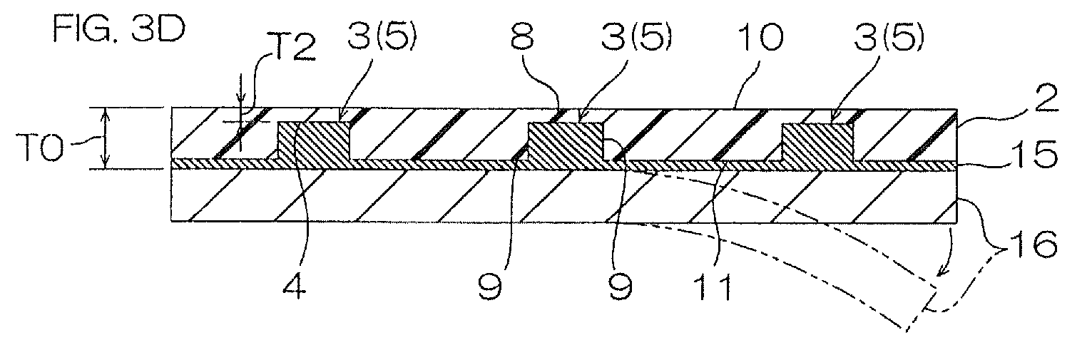
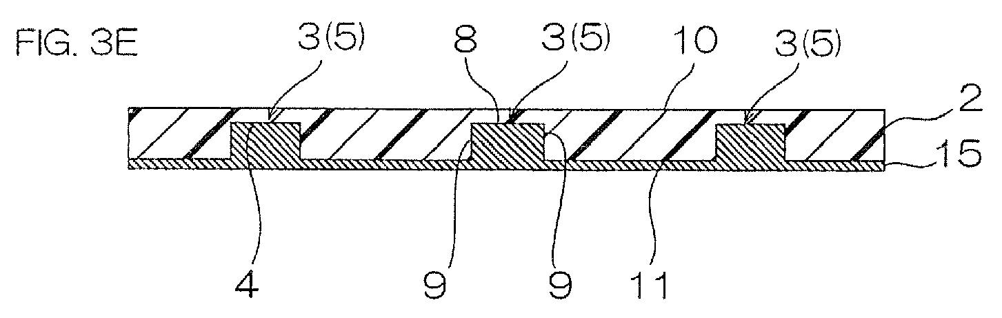
- the producing method includes a step (1) of forming the seed layer 15 on the upper surface (one example of one surface in the thickness direction) of a peeling layer 16 (ref: FIG. 3A ), a step (2) of forming the conductive patterns 3 on the upper surface (one example of one surface in the thickness direction) of the seed layer 15 (ref: FIGS. 3B and 3C ), a step (3) of covering the seed layer 15 and the conductive patterns 3 with the insulating layer 2 (ref: FIG. 3D ), a step (4) of peeling the peeling layer 16 from the seed layer 15 (ref: FIG. 3E ), and a step (5) of removing the seed layer 15 (ref: FIG. 3F ).
- the wired circuit board 1 is, for example, produced by a roll-to-roll method or a single wafer (batch) method.
- the seed layer 15 is formed on the upper surface (one example of one surface in the thickness direction) of the peeling layer 16.
- the seed layer 15 is, for example, formed of a metal material such as chromium, gold, silver, platinum, nickel, titanium, silicon, manganese, zirconium, and an alloy thereof or an oxide thereof.
- a metal material such as chromium, gold, silver, platinum, nickel, titanium, silicon, manganese, zirconium, and an alloy thereof or an oxide thereof.
- the metal material preferably, copper is used.
- the peeling layer 16 is not particularly limited as long as it is a supporting layer capable of supporting the seed layer 15 and being peeled therefrom. Examples thereof include a resin layer and a metal layer. Preferably, a metal layer is used.
- the metal layer is, for example, formed from a metal material such as stainless steel, aluminum, and 42-alloy into a sheet shape. As the metal material, preferably, stainless steel is used.
- a thickness of the peeling layer 16 is, for example, 18 ⁇ m or more, preferably 30 ⁇ m or more, and for example, 200 ⁇ m or less, preferably 100 ⁇ m or less.
- the seed layer 15 is formed on the upper surface of the peeling layer 16 by preferably plating, more preferably, electrolytic plating.
- the seed layer 15 is formed on the entire upper surface of the peeling layer 16.
- a thickness of the seed layer 15 is, for example, 0.03 ⁇ m or more, preferably 0.3 ⁇ m or more, and for example, 5 ⁇ m or less, preferably 3 ⁇ m or less.
- the step (2) is performed after the step (1).
- the conductive patterns 3 are formed on the upper surface of the seed layer 15.
- the conductive patterns 3 are formed on the upper surface of the seed layer 15 by an additive method.
- plating resists 17 are formed from a dry film resist on the upper surface of the seed layer 15 in a pattern reverse to the conductive patterns 3.
- the conductive patterns 3 are laminated on portions that are exposed from the plating resists 17 on the upper surface of the seed layer 15 by electrolytic plating that supplies electricity from the seed layer 15.
- the plating resists 17 shown by phantom lines of FIG. 3C are, for example, removed by using a peeling solution.
- the conductive patterns 3 have a shape continuous to the upper surface of the seed layer 15.
- the step (3) is performed after the step (2).
- the seed layer 15 and the conductive patterns 3 are covered with the insulating layer 2.
- the insulating layer 2 made of a semi-solid or solid (to be more specific, B-stage) insulating material that is formed into a sheet shape in advance is prepared, and subsequently, the prepared insulating layer 2 is compressively bonded or transferred to the seed layer 15 and the conductive pattern 3.
- a liquid (to be more specific, A-stage) insulating material (varnish or the like) is applied to the seed layer 15 and the conductive pattern 3.
- the insulating material is allowed to cure (brought into a C-stage state) by ultraviolet irradiation or heating.
- the insulating layer 2 filling a space between the conductive patterns 3 and the outside of the conductive patterns 3 is formed on the upper surface of the seed layer 15 so as to cover the conductive patterns 3 and the seed layer 15.
- the insulating layer 2 covers the upper surface of the seed layer 15, facing surfaces 8 of the conductive patterns 3 (in FIG. 3D , corresponding to the upper surfaces 8 and meanwhile, in FIG. 2 , corresponding to the lower surfaces 8), and the side surfaces 9 thereof.
- the portions covering the facing surfaces 8 and the side surfaces 9 of the conductive patterns 3 are the ditch portions 4.
- the step (4) is performed after the step (3).
- the peeling layer 16 is peeled from the seed layer 15.
- the peeling layer 16 is peeled from the seed layer 15, while being deflected downwardly.
- the right end portion of the peeling layer 16 is held and pulled downwardly so as to deflect the peeling layer 16 to be curved downwardly, so that the right end portion, the central portion in the right-left direction, and the left end portion of the peeling layer 16 are sequentially peeled from the right end portion, the central portion in the right-left direction, and the left end portion of the lower surface of the seed layer 15, respectively.
- the step (5) is performed after the step (4).
- the seed layer 15 is removed.
- the seed layer 15 is, for example, removed by etching such as wet etching.
- the lower end portions of the conductive patterns 3 filling the ditch portions 4 are removed. In this manner, the step portions 21 are formed.
- the thickness T6 of the lower end portion of the conductive pattern 3 that is removed is the same as the depth T6 of the step portion 21 described above.
- the wired circuit board 1 shown in FIGS. 1 and 2 is obtained by the above-described steps (1) to (5).
- the wearable device 20 includes the wired circuit board 1, the sensor 18 (the phantom lines), and the memory 25 (the phantom lines).
- a covering layer 19 and a pressure-sensitive adhesive layer 23 are provided in the wired circuit board 1 as needed.
- the covering layer 19 is formed on the upper surface 11 of the insulating layer 2 so as to cover the wires 5, and is formed of an insulating material or the like illustrated in the insulating layer 2.
- the pressure-sensitive adhesive layer 23 is provided on the lower surface of the insulating layer 2.
- the sensor 18 is, for example, a measurement means capable of measuring data such as a pulse, a body temperature or the like of a user.
- the sensor 18 is electrically connected to the terminals 6 at the front end portion of the wired circuit board 1.
- the memory 25 is a memory means capable of memorizing data measured by the sensor 18.
- the memory 25 is electrically connected to the terminals 6 at the rear end portion of the wired circuit board 1.
- the wearable device 20 is, for example, attached to (mounted on) the skin of the inner-side portion of a wrist 24 of a user by the pressure-sensitive adhesive layer 23.
- the wearable device 20 flexibly follows the extension of the wrist 24 (transfer to the back of the hand) as shown in FIG. 4B and the bending of the wrist 24 (transfer to the palm of the hand) as shown in FIG. 4C .
- the skin of the inner-side portion of the wrist 24 extends by the extension of the wrist 24, and following this movement, the wired circuit board 1 of the wearable device 20 extends.
- the skin of the inner-side portion of the wrist 24 bends by the bending of the wrist 24, and following this movement, the wired circuit board 1 of the wearable device 20 bends.
- the insulating layer 2 has the number of times of folding endurance measured in conformity with JIS P8115 (2001) of the above-described lower limit or more, so that the wired circuit board 1 has excellent elastic properties.
- the insulating layer 2 is formed of at least one kind of insulating material selected from the group consisting of polyurethane resin, (meth)acrylic resin, urethane-(meth)acrylic resin, silicone resin, polyolefin resin, polyvinyl chloride resin, polyvinylidene chloride resin, polyvinyl acetate resin, fluorine resin, styrene resin, butadiene resin, and isobutylene resin
- the insulating layer 2 can have both flexibility and toughness.
- the wired circuit board 1 has excellent elastic properties and excellent reliability.
- the wired circuit board 1 includes the wearable device 20.
- the usages of the wired circuit board 1 are not particularly limited, and preferably, the wired circuit board 1 is used for the usages demanding elastic properties.
- the upper surface 7 of the conductive pattern 3 is positioned at the lower side with respect to the upper surface 11 of the insulating layer 2.
- the upper surface 7 of the conductive pattern 3 can be also positioned so as to be flush with the upper surface 11 of the insulating layer 2.
- the upper surface 7 of the conductive pattern 3 and the upper surface 11 of the insulating layer 2 are positioned at the same position when projected in a plane direction (the front-rear direction and the right-left direction). In this manner, the upper surface 7 of the conductive pattern 3 and the upper surface 11 of the insulating layer 2 form a single flat surface. That is, the step portion 21 (ref: FIG. 2 ) in one embodiment is not formed on the upper surface of the wired circuit board 1.
- the etching time is adjusted so that only the seed layer 15 is removed, and the lower end potions of the conductive patterns 3 filling the ditch portions 4 are not removed.
- wired circuit board 1 shown in FIG. 5 the same function and effect as that of the wired circuit board 1 of one embodiment can be achieved.
- the wired circuit board 1 of one embodiment is preferable in view of suppressing blocking with the roll with respect to the wired circuit board 1 shown in FIG. 5 .
- the wired circuit board 1 of one embodiment shown in FIG. 2 when the wired circuit board 1 is produced by a roll-to-roll method and the upper surface of the wired circuit board 1 faces a roll (not shown), a gap (space) between the upper surface 7 of the conductive pattern 3 and the surface of the roll can be provided, which is different from the wired circuit board 1 shown in FIG. 5 .
- the contact area with the roll on the upper surface of the wired circuit board 1 can be reduced.
- blocking of the wired circuit board 1 of one embodiment shown in FIG. 2 with the roll can be suppressed, compared to the wired circuit board 1 shown in FIG. 5 .
- the upper surface 7 of the conductive pattern 3 can be also positioned at the upper side with respect to the upper surface 11 of the insulating layer 2.
- the lower end portion and the central portion of the conductive pattern 3 are embedded in the insulating layer 2, while the upper end portion thereof protrudes upwardly with respect to the upper surface 11 of the insulating layer 2.
- An embedded depth T4 (that is, distance T4 in the thickness direction between the lower surface 8 of the conductive pattern 3 and the upper surface 11 of the insulating layer 2) of the conductive pattern 3, a protruding length T5 (that is, distance T5 in the thickness direction between the upper surface 7 of the conductive pattern 3 and the upper surface 11 of the insulating layer 2) of the conductive pattern 3, and the ratio (T4/T5) of the embedded depth T4 to the protruding length T5 of the conductive pattern 3 are appropriately set in accordance with its usages and purpose.
- a dry film resist (not shown) is laminated on the lower surface of the seed layer 15; next, an etching resist (not shown) having the same pattern as the conductive pattern 3 is formed from the dry film resist by exposure to light and development; and thereafter, only the seed layer 15 that is exposed from the etching resist is removed. Thereafter, the etching resist is removed.
- the wired circuit board 1 shown in FIGS. 2 and 5 is preferable, compared to the wired circuit board 1 shown in FIG. 6 .
- the upper surface 7 of the conductive pattern 3 is positioned at the lower side of or at the same position as the upper surface 11 of the insulating layer 2, which is different from the wired circuit board 1 shown in FIG. 6 , so that a short circuit between the conductive patterns 3 can be suppressed.
- the conductive pattern 3 has a generally rectangular shape when viewed in cross section.
- the conductive pattern 3 can also have a generally tapered shape when viewed in cross section.
- the conductive pattern 3 has a generally tapered shape when viewed in cross section in which the length (width) in the right-left direction thereof gradually becomes short (narrow) toward the upper side.
- the side surfaces 9 that face each other in the right-left direction incline so as to gradually get close to each other toward the upper side.
- the length (width) in the right-left direction of the lower surface 8 in the wire 5 with respect to the length (width) in the right-left direction of the upper surface 7 in the wire 5 is, for example, 101% or more, preferably 105% or more, and for example, 145% or less.
- an adhesive force of the conductive pattern 3 with respect to the insulating layer 2 can be further more improved by an anchor effect of the conductive pattern 3 with respect to the insulating layer 2.
- the pressure-sensitive adhesive layer 23 is provided in the wired circuit board 1, and the insulating layer 2 is attached to the skin of the inner-side portion of the wrist 24 of the user via the pressure-sensitive adhesive layer 23.
- the insulating layer 2 of the wired circuit board 1 can be also directly attached (bonded) to the skin of the inner-side portion of the wrist 24 of the user without providing the pressure-sensitive adhesive layer 23.
- the peeling layer 16 made of stainless steel and having a thickness of 50 ⁇ m was prepared, and subsequently, the seed layer 15 made of copper and having a thickness of 1.0 ⁇ m was formed on the upper surface of the peeling layer 16 by electrolytic copper plating (the step (1), ref: FIG. 3A ).
- a dry film resist was laminated on the entire upper surface of the seed layer 15 and next, the plating resists 17 were formed on the upper surface of the seed layer 15 in a pattern reverse to the conductive patterns 3 by exposing the dry film resist to light to be developed (ref: FIG. 3B ).
- the conductive patterns 3 made of copper and having a thickness of 3 ⁇ m were laminated on the upper surface of the seed layer 15 by electrolytic copper plating that supplied electricity from the seed layer 15.
- the plating resists 17 were removed by using a peeling solution (ref: the phantom lines of FIG. 3C , the step (2)).
- a length in the right-left direction of each of the plurality of wires 5 was 50 ⁇ m and a length in the front-rear direction thereof was 60 mm. An interval between the wires 5 that were next to each other was 4050 ⁇ m. A length in the right-left direction and a length in the front-rear direction of each of the plurality of terminals 6 were 4000 ⁇ m. An interval between the terminals 6 that were next to each other was 100 ⁇ m.
- the plane area S1 of the conductive pattern 3 was 70 mm 2 .
- a varnish of a mixture (urethane-acrylic resin) prepared by formulations described in the "Details” column of "Insulating Material” described in Table 1 was applied to the seed layer 15 and the conductive pattern 3. Thereafter, the varnish in an A-stage state and B-stage state was allowed to cure (brought into a C-stage state) by applying an ultraviolet ray (irradiance: 340 mW/cm 2 , amount of light: 4000 mJ/cm 2 ) by using a high pressure mercury lamp, so that the insulating layer 2 was formed (the step (3), ref: FIG. 3D ).
- an ultraviolet ray irradiance: 340 mW/cm 2 , amount of light: 4000 mJ/cm 2
- the thickness T0 of the insulating layer 2 was 10 ⁇ m.
- the thickness T2 of the insulating layer 2 facing the conductive pattern 3 was 7 ⁇ m.
- the depth of the ditch portion 4 was 3 ⁇ m.
- the ratio ((T1 + T6)/T0) of the depth (corresponding to T1 + T6 to be described later) of the ditch portion 4 to the thickness T0 of the insulating layer 2 was 0.3.
- the plane area S0 of the insulating layer 2 was 1600 mm 2 , and the ratio of S1/S0 was 4.375%.
- the peeling layer 16 was peeled from the seed layer 15 (the step (4), ref: FIG. 3E ).
- the seed layer 15 was removed by wet etching (the step (5), ref: FIG. 3F ). Furthermore, along with the removal of the seed layer 15, the lower end portions of the conductive patterns 3 filling the ditch portions 4 were removed.
- the thickness T6 of the lower end portion of the conductive pattern 3 that was removed was 2 ⁇ m.
- the thickness T1 of the conductive pattern 3 was 1 ⁇ m.
- the ratio of T1/T2 was 0.143, the ratio of T6/T0 was 0.2, the ratio of T1/T0 was 0.1, and the ratio of T2/T0 was 0.7.
- the wired circuit board 1 including the insulating layer 2 and the conductive pattern 3 was obtained (ref: FIGS. 1 and 2 ).
- a wired circuit board 1 was obtained in the same manner as that of Example 1, except that the size and the arrangement of the conductive pattern 3, and the type, the details, and the curing conditions of the insulating material were changed in accordance with the descriptions in Table 1 (ref: FIGS. 2 and 6 ).
- Example 7 an etching resist was formed in the same pattern as that of the conductive pattern 3; thereafter, only the seed layer 15 that was exposed from the etching resist was removed; and then, the etching resist was removed. In this manner, in Example 6, the upper surface 7 of the conductive pattern 3 was positioned at the upper side with respect to the upper surface 11 of the insulating layer 2.
- the tensile storage elastic modulus E' at 20°C of only each of the insulating layers 2 of Examples and Comparative Examples was measured by a dynamic viscoelasticity measurement method (DMA method) under the conditions of a temperature range of -10 to 260°C, a frequency of 1 Hz, and a temperature rising rate of 10°C/min.
- DMA method dynamic viscoelasticity measurement method
- the number of times of folding endurance of only each of the insulating layers 2 of Examples and Comparative Examples was counted by carrying out a MIT test (folding endurance test) under the following conditions in conformity with JIS P8115 (2001). Then, the folding endurance was evaluated in accordance with the following reference.
- a pressure-sensitive adhesive tape (No. 360UL, manufactured by NITTO DENKO CORPORATION) was attached to each of the upper surfaces of the wired circuit board 1 of Examples and Comparative Examples, and then, the pressure-sensitive adhesive tape was peeled from the wired circuit board 1. Subsequently, the movement of the above-described attachment and peeling was repeated. Then, the number of times required for peeling the conductive pattern 3 from the insulating layer 2 was obtained, and the adhesive properties were evaluated in accordance with the following reference.
- a probe was touched to two wires that were electrically independent and next to each other, and a presence or absence of electrical conduction was checked based on resistance values of a digital multimeter by using a two-terminal resistance mode of a digital multimeter (ADVANTEST R6552 DIGITAL MULTIMETER).
- the wired circuit board obtained by the method for producing a wired circuit board is, for example, used in the wearable device.
Landscapes
- Engineering & Computer Science (AREA)
- Microelectronics & Electronic Packaging (AREA)
- Manufacturing & Machinery (AREA)
- Manufacturing Of Printed Wiring (AREA)
- Structure Of Printed Boards (AREA)
Abstract


Description
- The present invention relates to a method for producing a wired circuit board.
- A wired circuit board such as printed wiring board is produced by various producing methods.
- For example, a method for producing a printed wiring board has been proposed in which a metal film is provided on the surface of a metal material and a transfer circuit is provided on the surface of the metal film, so that a transfer substrate is produced; the transfer substrate is attached to a resin layer to embed the transfer circuit into the resin layer; and thereafter, the metal material is peeled and the metal film is removed by etching (ref: for example, Patent Document 1).
- In the method for producing the printed wiring board described in
Patent Document 1, as the resin layer, a prepreg that is formed by impregnating a thermosetting resin such as epoxy resin in a substrate such as glass fabric to be dried by heating until being brought into a B-stage state and an adhesive sheet such as adhesive film that is formed by molding a thermosetting resin such as epoxy resin into a film shape to be dried by heating until being brought into a B-stage state are used. - Patent Document 1: Japanese Unexamined Patent Publication No.
2010-80568 - Recently, when a wired circuit board is included in a wearable device, excellent elastic properties are demanded. However, there is a disadvantage that the printed wiring board obtained by the producing method described in
Patent Document 1 cannot satisfy the above-described demand. - An object of the present invention is to provide a method for producing a wired circuit board having excellent elastic properties.
- The present invention [1] includes a method for producing a wired circuit board including a step (1) of forming a seed layer on one surface in a thickness direction of a peeling layer, a step (2) of forming a conductive pattern on one surface in the thickness direction of the seed layer, a step (3) of covering the seed layer and the conductive pattern with an insulating layer, a step (4) of peeling the peeling layer from the seed layer, and a step (5) of removing the seed layer, wherein the insulating layer has the number of times of folding endurance measured in conformity with JIS P8115 (2001) of 10 times or more.
- According to the structure, the insulating layer has the number of times of folding endurance measured in conformity with JIS P8115 (2001) of the above-described lower limit or more, so that the wired circuit board has excellent elastic properties.
- The present invention [2] includes the method for producing a wired circuit board described in the above-described [1], wherein the insulating layer is formed of at least one kind of insulating material selected from the group consisting of polyurethane resin, (meth)acrylic resin, urethane-(meth)acrylic resin, silicone resin, polyolefin resin, polyvinyl chloride resin, polyvinylidene chloride resin, polyvinyl acetate resin, fluorine resin, styrene resin, butadiene resin, and isobutylene resin.
- According to the structure, the insulating layer can have both flexibility and toughness. Thus, the wired circuit board has excellent elastic properties and excellent reliability.
- The wired circuit board of the present invention has excellent elastic properties.
-
-
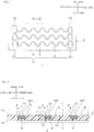
FIG. 1 shows a plan view of a wired circuit board obtained by one embodiment of a method for producing a wired circuit board of the present invention. -
FIG. 2 shows a cross-sectional view of the wired circuit board shown inFIG. 1 and a cross-sectional view in a right-left direction along an A-A line. -
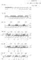
FIGS. 3A to 3F show process drawings for illustrating a method for producing the wired circuit board shown inFIG. 2 : -
FIG. 3A illustrating a step (1) of forming a seed layer on the upper surface of a peeling layer, -
FIG. 3B illustrating a step of forming plating resists on the upper surface of the seed layer, -
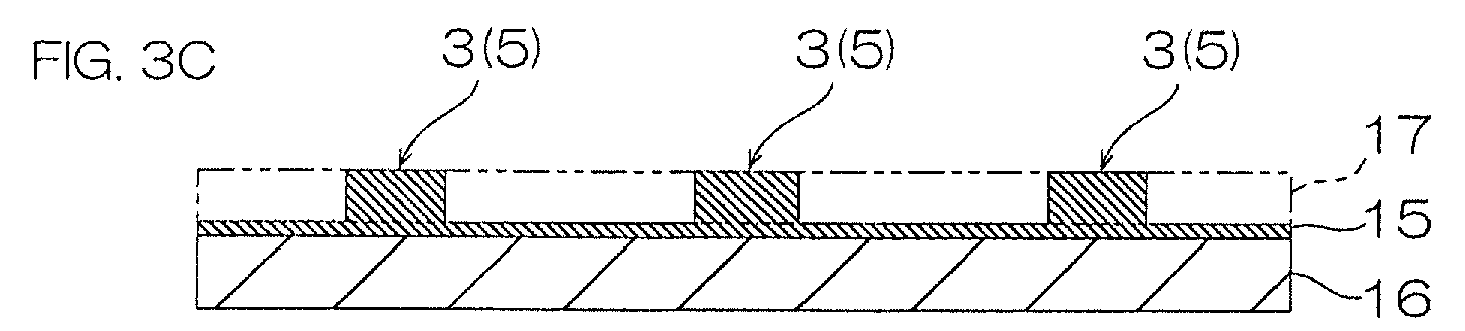
FIG. 3C illustrating a step (2) of forming conductive patterns on the upper surface of the seed layer, -
FIG. 3D illustrating a step (3) of covering the seed layer and the conductive patterns with an insulating layer, -
FIG. 3E illustrating a step (4) of peeling the peeling layer from the seed layer, and -
FIG. 3F illustrating a step (5) of removing the seed layer. -
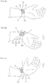
FIGS. 4A to 4C show embodiments in which a wearable device including the wired circuit board shown inFIG. 1 is attached to the skin of the inner-side portion of a wrist: -
FIG. 4A illustrating a state in which the wrist is not extended or bended, -
FIG. 4B illustrating a state in which the wrist is extended, and -
FIG. 4C illustrating a state in which the wrist is bended. -
FIG. 5 shows an enlarged cross-sectional view of a wired circuit board (embodiment in which the upper surface of the conductive pattern is flush with the upper surface of the insulating layer) of a modified example of one embodiment. -
FIG. 6 shows an enlarged cross-sectional view of a wired circuit board (embodiment in which the upper surface of the conductive pattern is positioned at the upper side with respect to the upper surface of the insulating layer) of a modified example of one embodiment. -
FIG. 7 shows an enlarged cross-sectional view of a wired circuit board (embodiment in which the conductive pattern has a generally tapered shape when viewed in cross section) of a modified example of one embodiment. - In
FIG. 2 , the right-left direction of the paper surface is a right-left direction (first direction), the left side of the paper surface is a left side (one side in the first direction), and the right side of the paper surface is a right side (the other side in the first direction). InFIG. 2 , the up-down direction of the paper surface is an up-down direction (second direction perpendicular to the first direction, thickness direction), the upper side of the paper surface is an upper side (one side in the second direction, one side in the thickness direction), and the lower side of the paper surface is a lower side (the other side in the second direction, the other side in the thickness direction). InFIG. 2 , the depth direction of the paper surface is a front-rear direction (third direction perpendicular to the first direction and the second direction, longitudinal direction (ref:FIG. 1 )), the near side of the paper surface is a front side (one side in the third direction, one side in the longitudinal direction), and the far side of the paper surface is a rear side (the other side in the third direction, the other side in the longitudinal direction). To be specific, the directions are in conformity with the direction arrows in each figure. - In
FIGS. 4A to 4C , asensor 18 and a memory 25 (described later) are omitted so as to clearly show the shape of a wired circuit board 1 (described later). - As shown in
FIGS. 1 and 2 , thewired circuit board 1 that is one embodiment of the present invention includes aninsulating layer 2 andconductive patterns 3 that are embedded in theinsulating layer 2. - As shown in
FIG. 1 , theinsulating layer 2 has the same outer shape as that of thewired circuit board 1. To be specific, theinsulating layer 2 has a film (sheet) shape in a generally rectangular shape when viewed from the top extending in the front-rear direction. As shown inFIG. 2 , theinsulating layer 2 includes a flatlower surface 10 and anupper surface 11 facing the upper side of thelower surface 10 at spaced intervals thereto. Theinsulating layer 2 includes a plurality ofditch portions 4 corresponding to theconductive patterns 3. Each of the plurality ofditch portions 4 has an opening upwardly. - The insulating
layer 2 is, for example, formed of an insulating material that satisfies the number of times of folding endurance to be described later. Examples of the insulating material include polyurethane resin, (meth)acrylic resin (meaning acrylic resin and/or methacrylic resin, hereinafter, the same), urethane-(meth)acrylic resin, silicone resin, polyolefin resin (to be specific, polyethylene resin, polypropylene resin, or the like), polyvinyl chloride resin, polyvinylidene chloride resin, polyvinyl acetate resin, fluorine resin, styrene resin, butadiene resin, and isobutylene resin. The insulating materials can be used alone or in combination of two or more. - As the insulating material, in order to obtain characteristics of having both flexibility and toughness, preferably, polyurethane resin, (meth)acrylic resin, urethane-(meth)acrylic resin, and silicone resin are used, and in view of obtaining excellent folding endurance, more preferably, urethane-(meth)acrylic resin and silicone resin are used.
- The urethane-(meth)acrylic resin is an ultraviolet curing resin, and is, for example, obtained by blending a material containing polyol, polyisocyanate, (meth)acrylic acid, and (meth)acrylate to be allowed to react under the presence of a photopolymerization initiator. To be specific, the above-described material and the above-described photopolymerization initiator are blended to prepare a mixture, and an ultraviolet ray is applied to the mixture to cure.
- The silicone resin is a thermosetting resin, and examples thereof include polydimethyl siloxane, polymethylphenyl siloxane, and polydiphenyl siloxane. Preferably, polydimethyl siloxane is used.
- The insulating
layer 2 has the number of times of folding endurance measured in conformity with JIS P8115 (2001) of 10 times or more, preferably 100 times or more, more preferably, 1000 times or more, further more preferably, 10000 times or more and, for example, 100000 times or less. When the number of times of folding endurance of the insulatinglayer 2 is below the above-described lower limit, the peeling of theconductive pattern 3 from the insulatinglayer 2 cannot be suppressed at the time of repeatedly expanding or contracting the wiredcircuit board 1. - The details of the measurement method of the number of times of folding endurance of the insulating
layer 2 are described in Examples later. - A tensile storage elastic modulus E' at 20°C of the insulating
layer 2 is, for example, 2000 MPa or less, preferably 1000 MPa or less, more preferably 100 MPa or less, further more preferably 50 MPa or less, particularly preferably 20 MPa or less, and for example, 0.1 MPa or more, preferably 0.5 MPa or more. - When the tensile storage elastic modulus E' of the insulating
layer 2 is the above-described upper limit or less, excellent elastic properties of the insulatinglayer 2 can be ensured. Meanwhile, when the tensile storage elastic modulus E' of the insulatinglayer 2 is the above-described lower limit or more, excellent toughness and excellent handleability can be ensured. - The tensile storage elastic modulus E' at 20°C of the insulating
layer 2 is obtained by subjecting the insulatinglayer 2 to dynamic viscoelasticity measurement under the conditions of a frequency of 1 Hz and a temperature rising rate of 10°C/min. - A thickness T0 of the insulating
layer 2 is, for example, 5 µm or more, preferably 10 µm or more, and for example, 1000 µm or less, preferably 300 µm or less. - As shown in
FIG. 2 , the thickness T0 of the insulatinglayer 2 is a distance T0 in the thickness direction between thelower surface 10 and theupper surface 11 of the insulatinglayer 2 in a region that is not overlapped with theconductive patterns 3 when projected in the thickness direction. - The thickness T0 of the insulating
layer 2 is the same as the thickness of the wiredcircuit board 1. - As shown in
FIGS. 1 and 2 , theconductive patterns 3 are disposed so as to be included in a projected surface of the insulatinglayer 2 when projected in the thickness direction. Theconductive patterns 3 integrally includewires 5 extending in the front-rear direction andterminals 6 that are connected to both end portions in the front-rear direction of thewires 5. - The plurality of
wires 5 are provided at spaced intervals to each other in the right-left direction. Each of the plurality ofwires 5 has a generally wave shape (or sine wave shape). - The plurality of
terminals 6 are provided in the front end portion and the rear end portion of the wiredcircuit board 1. Each of the plurality ofterminals 6 is provided so as to be continuous to both end portions in the front-rear direction of thewires 5. Each of the plurality ofterminals 6 is a land having a generally rectangular shape when viewed from the top. - As shown in
FIG. 2 , the conductive pattern 3 (to be specific, the wire 5) has a generally rectangular shape when viewed in cross section. To be specific, theconductive pattern 3 integrally has, as one example of an exposed surface, anupper surface 7, as one example of a facing surface, alower surface 8 that is disposed at the lower side (one example of the other side in the thickness direction) facing theupper surface 7 at spaced intervals thereto, and as one example of a connecting surface, side surfaces 9 that connect the periphery end portion of theupper surface 7 to the periphery end portion of thelower surface 8. Theconductive patterns 3 fit in theditch portions 4 so as to be exposed from theupper surface 11 of the insulatinglayer 2. - The
upper surface 7 of theconductive pattern 3 is positioned at the lower side (one example of the other side in the thickness direction) with respect to theupper surface 11 of the insulatinglayer 2. Astep portion 21 with respect to theupper surface 11 of the insulatinglayer 2 is formed by theupper surface 7 of theconductive pattern 3 and the inner-side surfaces of theditch portion 4 that are at the upper side with respect to theupper surface 7. Theupper surface 7 of theconductive pattern 3 is a surface that is in parallel with theupper surface 11 of the insulatinglayer 2, and a flat surface extending in the front-rear direction. Furthermore, theupper surface 7 of theconductive pattern 3 is an exposed surface that is exposed from theupper surface 11 of the insulatinglayer 2. - The
lower surface 8 of theconductive pattern 3 is a flat surface that is in parallel with theupper surface 7 of theconductive pattern 3. Thelower surface 8 of theconductive pattern 3 is covered with the inner-side surfaces of theditch portion 4 of the insulatinglayer 2. To be specific, thelower surface 8 of theconductive pattern 3 is in direct contact with theditch portion 4 of the insulatinglayer 2. - The side surfaces 9 of the
conductive pattern 3 are surfaces along the thickness direction (the up-down direction), and are covered with the inner-side surfaces of theditch portion 4 of the insulatinglayer 2. The side surfaces 9 of theconductive pattern 3 are in direct contact with theditch portion 4 of the insulatinglayer 2. - The
conductive pattern 3 is, for example, formed of a conductive material such as copper, nickel, and gold or an alloy thereof. As the conductive material, preferably, copper is used. - The size of the
conductive pattern 3 is appropriately set in accordance with its usages and purpose, and is not particularly limited. A length (width) in the right-left direction of each of the plurality ofwires 5 is for example, 12 µm or more, preferably 15 µm or more, and for example, 1000 µm or less, preferably 750 µm or less. An interval between thewires 5 that are next to each other is, for example, 12 µm or more, preferably 15 µm or more, and for example, 10000 µm or less, preferably 7500 µm or less. A length (width) in the front-rear direction of each of the plurality ofwires 5 is, for example, 10 mm or more, preferably 20 mm or more, and for example, 250 mm or less, preferably 100 mm or less. A length in the right-left direction and a length in the front-rear direction of each of the plurality ofterminals 6 are, for example, 100 µm or more, preferably 200 µm or more, and for example, 10000 µm or less, preferably 5000 µm or less. An interval between theterminals 6 that are next to each other is, for example, 50 µm or more, preferably 100 µm or more, and for example, 10000 µm or less, preferably 5000 µm or less. - The ratio (S1/S0) of a plane area S1 (projected area when projected in the thickness direction) of the
conductive pattern 3 to a plane area S0 of the insulatinglayer 2, that is, the ratio of theconductive pattern 3 to the insulatinglayer 2 when projected in the thickness direction is, for example, 70% or less, preferably 60% or less, and for example, 1% or more, preferably 3% or more. When the ratio of S1/S0 is the above-described upper limit or less, the wiredcircuit board 1 has excellent elastic properties. - A thickness T1 (distance T1 in the thickness direction between the
upper surface 7 and the lower surface 8) of theconductive pattern 3, that is, the thickness T1 of each of thewires 5 and theterminals 6 is, for example, 0.3 µm or more, preferably 0.8 µm or more, more preferably 1.0 µm or more, and for example, 112 µm or less, preferably 75 µm or less, more preferably 40 µm or less. When the thickness T1 of theconductive pattern 3 is the above-described lower limit or more, an adhesive force of theconductive pattern 3 with respect to the insulatinglayer 2 can be improved, and the peeling of theconductive pattern 3 from the insulatinglayer 2 can be suppressed. - The ratio (T1/T0) of the thickness T1 of the
conductive pattern 3 to the thickness T0 of the insulatinglayer 2 is, for example, below 1, preferably 0.9 or less, more preferably 0.8 or less, and for example, 0.05 or more, preferably 0.1 or more, more preferably 0.2 or more. When the ratio of T1/T0 is the above-described lower limit or more, thinning of the wiredcircuit board 1 can be achieved. - A thickness T2 of the insulating
layer 2 that is positioned at the lower side of theconductive pattern 3, that is, the thickness T2 of the insulatinglayer 2 facing theconductive pattern 3 in the thickness direction is, for example, 200 µm or less, preferably 150 µm or less, more preferably 10 µm or less, and for example, 5 µm or more. - The ratio (T2/T0) of the thickness T2 of the insulating
layer 2 that is positioned at the lower side of theconductive pattern 3 to the thickness T0 of the insulatinglayer 2 is, for example, 0.95 or less, preferably 0.85 or less, more preferably 0.75 or less, and for example, 0.1 or more. When the ratio of T2/T0 is the above-described upper limit or less, thinning of the wiredcircuit board 1 can be achieved, while an adhesive force of theconductive pattern 3 with respect to the insulatinglayer 2 is ensured. - The ratio (T1/T2) of the thickness T1 of the
conductive pattern 3 to the thickness T2 of the insulatinglayer 2 that is positioned at the lower side of theconductive pattern 3 is, for example, 0.05 or more, preferably 0.1 or more, and for example, 0.9 or less, preferably 0.8 or less. When the ratio of T1/T2 is the above-described lower limit or more, thinning of the wiredcircuit board 1 can be achieved. - A distance T6 in the thickness direction between the
upper surface 7 of theconductive pattern 3 and theupper surface 11 of the insulatinglayer 2, that is, a depth T6 of the above-describedstep portion 21 is, for example, 0.5 µm or more, preferably 1 µm or more, and for example, 10 µm or less, preferably 5 µm or less. - The ratio (T6/T0) of the depth T6 of the
step portion 21 to the thickness T0 of the insulatinglayer 2 is, for example, 0.01 or more, preferably 0.03 or more, and for example, 0.5 or less, preferably 0.3 or less. When the ratio of T6/T0 is the above-described lower limit or more, the time to remove aseed layer 15 in a step (5) to be described later can be sufficiently ensured, so that a short circuit of theconductive patterns 3 that are next to each other via theseed layer 15 can be suppressed. - The sum (T1 + T6) of the thickness T1 of the
conductive pattern 3 and the depth T6 of thestep portion 21 is a depth of theditch portion 4, and is, for example, 1 µm or more, preferably 10 µm or more, and for example, 300 µm or less, preferably 100 µm or less. - The ratio ((T1 + T6)/T0) of the depth (T1 + T6) of the
ditch portion 4 to the thickness T0 of the insulatinglayer 2 is, for example, 0.1 or more, preferably 0.2 or more, and for example, 0.9 or less, preferably 0.8 or less. When the above-described ratio is the above-described lower limit or more, thinning of the wiredcircuit board 1 can be achieved, while an adhesive force of theconductive pattern 3 with respect to the insulatinglayer 2 is ensured. - Next, a method for producing the wired
circuit board 1 is described with reference toFIGS. 3A to 3F . - The producing method includes a step (1) of forming the
seed layer 15 on the upper surface (one example of one surface in the thickness direction) of a peeling layer 16 (ref:FIG. 3A ), a step (2) of forming theconductive patterns 3 on the upper surface (one example of one surface in the thickness direction) of the seed layer 15 (ref:FIGS. 3B and 3C ), a step (3) of covering theseed layer 15 and theconductive patterns 3 with the insulating layer 2 (ref:FIG. 3D ), a step (4) of peeling thepeeling layer 16 from the seed layer 15 (ref:FIG. 3E ), and a step (5) of removing the seed layer 15 (ref:FIG. 3F ). - In the producing method, the wired
circuit board 1 is, for example, produced by a roll-to-roll method or a single wafer (batch) method. - In the following, each of the steps is described.
- In the step (1), as shown in
FIG. 3A , theseed layer 15 is formed on the upper surface (one example of one surface in the thickness direction) of thepeeling layer 16. - The
seed layer 15 is, for example, formed of a metal material such as chromium, gold, silver, platinum, nickel, titanium, silicon, manganese, zirconium, and an alloy thereof or an oxide thereof. As the metal material, preferably, copper is used. - The
peeling layer 16 is not particularly limited as long as it is a supporting layer capable of supporting theseed layer 15 and being peeled therefrom. Examples thereof include a resin layer and a metal layer. Preferably, a metal layer is used. The metal layer is, for example, formed from a metal material such as stainless steel, aluminum, and 42-alloy into a sheet shape. As the metal material, preferably, stainless steel is used. A thickness of thepeeling layer 16 is, for example, 18 µm or more, preferably 30 µm or more, and for example, 200 µm or less, preferably 100 µm or less. - To form the
seed layer 15 on the upper surface of thepeeling layer 16, for example, a wet process such as plating and a dry process such as vacuum deposition and sputtering are used. Theseed layer 15 is formed on the upper surface of thepeeling layer 16 by preferably plating, more preferably, electrolytic plating. - The
seed layer 15 is formed on the entire upper surface of thepeeling layer 16. - A thickness of the
seed layer 15 is, for example, 0.03 µm or more, preferably 0.3 µm or more, and for example, 5 µm or less, preferably 3 µm or less. - The step (2) is performed after the step (1). In the step (2), as shown in
FIG. 3C , theconductive patterns 3 are formed on the upper surface of theseed layer 15. - As shown in
FIGS. 3B and 3C , preferably, theconductive patterns 3 are formed on the upper surface of theseed layer 15 by an additive method. - To be specific, first, as shown in
FIG. 3B , plating resists 17 are formed from a dry film resist on the upper surface of theseed layer 15 in a pattern reverse to theconductive patterns 3. Next, as shown inFIG. 3C , theconductive patterns 3 are laminated on portions that are exposed from the plating resists 17 on the upper surface of theseed layer 15 by electrolytic plating that supplies electricity from theseed layer 15. Thereafter, the plating resists 17 shown by phantom lines ofFIG. 3C are, for example, removed by using a peeling solution. - The
conductive patterns 3 have a shape continuous to the upper surface of theseed layer 15. - The step (3) is performed after the step (2). In the step (3), as shown in
FIG. 3D , theseed layer 15 and theconductive patterns 3 are covered with the insulatinglayer 2. - For example, the insulating
layer 2 made of a semi-solid or solid (to be more specific, B-stage) insulating material that is formed into a sheet shape in advance is prepared, and subsequently, the prepared insulatinglayer 2 is compressively bonded or transferred to theseed layer 15 and theconductive pattern 3. Or, a liquid (to be more specific, A-stage) insulating material (varnish or the like) is applied to theseed layer 15 and theconductive pattern 3. - Thereafter, when the semi-solid or solid insulating material, or the liquid insulating material is in an uncured state (A-stage state or B-stage state), the insulating material is allowed to cure (brought into a C-stage state) by ultraviolet irradiation or heating.
- In this manner, the insulating
layer 2 filling a space between theconductive patterns 3 and the outside of theconductive patterns 3 is formed on the upper surface of theseed layer 15 so as to cover theconductive patterns 3 and theseed layer 15. To be specific, the insulatinglayer 2 covers the upper surface of theseed layer 15, facingsurfaces 8 of the conductive patterns 3 (inFIG. 3D , corresponding to theupper surfaces 8 and meanwhile, inFIG. 2 , corresponding to the lower surfaces 8), and the side surfaces 9 thereof. In the insulatinglayer 2, the portions covering the facingsurfaces 8 and the side surfaces 9 of theconductive patterns 3 are theditch portions 4. - The step (4) is performed after the step (3). In the step (4), as shown in
FIG. 3E , thepeeling layer 16 is peeled from theseed layer 15. - To be specific, as shown by the phantom lines of
FIG. 3D , thepeeling layer 16 is peeled from theseed layer 15, while being deflected downwardly. For example, the right end portion of thepeeling layer 16 is held and pulled downwardly so as to deflect thepeeling layer 16 to be curved downwardly, so that the right end portion, the central portion in the right-left direction, and the left end portion of thepeeling layer 16 are sequentially peeled from the right end portion, the central portion in the right-left direction, and the left end portion of the lower surface of theseed layer 15, respectively. - The step (5) is performed after the step (4). In the step (5), as shown in
FIG. 3F , theseed layer 15 is removed. - The
seed layer 15 is, for example, removed by etching such as wet etching. - Along with the removal of the
seed layer 15, the lower end portions of theconductive patterns 3 filling theditch portions 4 are removed. In this manner, thestep portions 21 are formed. The thickness T6 of the lower end portion of theconductive pattern 3 that is removed is the same as the depth T6 of thestep portion 21 described above. - The wired
circuit board 1 shown inFIGS. 1 and 2 is obtained by the above-described steps (1) to (5). - Next, a wearable device 20 including the above-described
wired circuit board 1 is described. - As shown in
FIG. 1 , the wearable device 20 includes the wiredcircuit board 1, the sensor 18 (the phantom lines), and the memory 25 (the phantom lines). - As shown by the phantom lines of
FIG. 2 , acovering layer 19 and a pressure-sensitive adhesive layer 23 are provided in the wiredcircuit board 1 as needed. Thecovering layer 19 is formed on theupper surface 11 of the insulatinglayer 2 so as to cover thewires 5, and is formed of an insulating material or the like illustrated in the insulatinglayer 2. The pressure-sensitive adhesive layer 23 is provided on the lower surface of the insulatinglayer 2. - The
sensor 18 is, for example, a measurement means capable of measuring data such as a pulse, a body temperature or the like of a user. Thesensor 18 is electrically connected to theterminals 6 at the front end portion of the wiredcircuit board 1. - The
memory 25 is a memory means capable of memorizing data measured by thesensor 18. Thememory 25 is electrically connected to theterminals 6 at the rear end portion of the wiredcircuit board 1. - As shown in
FIG. 4A , the wearable device 20 is, for example, attached to (mounted on) the skin of the inner-side portion of awrist 24 of a user by the pressure-sensitive adhesive layer 23. - The wearable device 20 flexibly follows the extension of the wrist 24 (transfer to the back of the hand) as shown in
FIG. 4B and the bending of the wrist 24 (transfer to the palm of the hand) as shown inFIG. 4C . - To be specific, as shown in
FIG. 4B , the skin of the inner-side portion of thewrist 24 extends by the extension of thewrist 24, and following this movement, the wiredcircuit board 1 of the wearable device 20 extends. - Meanwhile, as shown in
FIG. 4C , the skin of the inner-side portion of thewrist 24 bends by the bending of thewrist 24, and following this movement, the wiredcircuit board 1 of the wearable device 20 bends. - In the wired
circuit board 1, the insulatinglayer 2 has the number of times of folding endurance measured in conformity with JIS P8115 (2001) of the above-described lower limit or more, so that the wiredcircuit board 1 has excellent elastic properties. - In the wired
circuit board 1, when the insulatinglayer 2 is formed of at least one kind of insulating material selected from the group consisting of polyurethane resin, (meth)acrylic resin, urethane-(meth)acrylic resin, silicone resin, polyolefin resin, polyvinyl chloride resin, polyvinylidene chloride resin, polyvinyl acetate resin, fluorine resin, styrene resin, butadiene resin, and isobutylene resin, the insulatinglayer 2 can have both flexibility and toughness. Thus, the wiredcircuit board 1 has excellent elastic properties and excellent reliability. - In the modified example, the same reference numerals are provided for members and steps corresponding to those described in one embodiment, and their detailed description is omitted.
- In one embodiment, the wired
circuit board 1 includes the wearable device 20. However, the usages of the wiredcircuit board 1 are not particularly limited, and preferably, the wiredcircuit board 1 is used for the usages demanding elastic properties. - In one embodiment, as shown in
FIG. 2 , theupper surface 7 of theconductive pattern 3 is positioned at the lower side with respect to theupper surface 11 of the insulatinglayer 2. Alternatively, for example, as shown inFIG. 5 , theupper surface 7 of theconductive pattern 3 can be also positioned so as to be flush with theupper surface 11 of the insulatinglayer 2. - That is, as shown in
FIG. 5 , theupper surface 7 of theconductive pattern 3 and theupper surface 11 of the insulatinglayer 2 are positioned at the same position when projected in a plane direction (the front-rear direction and the right-left direction). In this manner, theupper surface 7 of theconductive pattern 3 and theupper surface 11 of the insulatinglayer 2 form a single flat surface. That is, the step portion 21 (ref:FIG. 2 ) in one embodiment is not formed on the upper surface of the wiredcircuit board 1. - To obtain the wired
circuit board 1 shown inFIG. 5 , in the step (5) (ref:FIG. 3F ), the etching time is adjusted so that only theseed layer 15 is removed, and the lower end potions of theconductive patterns 3 filling theditch portions 4 are not removed. - In the wired
circuit board 1 shown inFIG. 5 , the same function and effect as that of the wiredcircuit board 1 of one embodiment can be achieved. - Meanwhile, the wired
circuit board 1 of one embodiment is preferable in view of suppressing blocking with the roll with respect to the wiredcircuit board 1 shown inFIG. 5 . - That is, in the wired
circuit board 1 of one embodiment shown inFIG. 2 , when the wiredcircuit board 1 is produced by a roll-to-roll method and the upper surface of the wiredcircuit board 1 faces a roll (not shown), a gap (space) between theupper surface 7 of theconductive pattern 3 and the surface of the roll can be provided, which is different from the wiredcircuit board 1 shown inFIG. 5 . Along with this, the contact area with the roll on the upper surface of the wiredcircuit board 1 can be reduced. Thus, blocking of the wiredcircuit board 1 of one embodiment shown inFIG. 2 with the roll can be suppressed, compared to the wiredcircuit board 1 shown inFIG. 5 . - Meanwhile, as shown in
FIG. 6 , theupper surface 7 of theconductive pattern 3 can be also positioned at the upper side with respect to theupper surface 11 of the insulatinglayer 2. - In the wired
circuit board 1 shown inFIG. 6 , the lower end portion and the central portion of theconductive pattern 3 are embedded in the insulatinglayer 2, while the upper end portion thereof protrudes upwardly with respect to theupper surface 11 of the insulatinglayer 2. - An embedded depth T4 (that is, distance T4 in the thickness direction between the
lower surface 8 of theconductive pattern 3 and theupper surface 11 of the insulating layer 2) of theconductive pattern 3, a protruding length T5 (that is, distance T5 in the thickness direction between theupper surface 7 of theconductive pattern 3 and theupper surface 11 of the insulating layer 2) of theconductive pattern 3, and the ratio (T4/T5) of the embedded depth T4 to the protruding length T5 of theconductive pattern 3 are appropriately set in accordance with its usages and purpose. - To obtain the wired
circuit board 1 shown inFIG. 6 , in the step (5) (ref:FIGS. 3E and 3F ), first, a dry film resist (not shown) is laminated on the lower surface of theseed layer 15; next, an etching resist (not shown) having the same pattern as theconductive pattern 3 is formed from the dry film resist by exposure to light and development; and thereafter, only theseed layer 15 that is exposed from the etching resist is removed. Thereafter, the etching resist is removed. - In the wired
circuit board 1 shown inFIG. 6 , the same function and effect as that of the wiredcircuit board 1 shown inFIG. 2 in one embodiment can be achieved. - Meanwhile, in view of suppressing a short circuit between the
conductive patterns 3, the wiredcircuit board 1 shown inFIGS. 2 and5 is preferable, compared to the wiredcircuit board 1 shown inFIG. 6 . - In the wired
circuit board 1 shown inFIGS. 2 and5 , theupper surface 7 of theconductive pattern 3 is positioned at the lower side of or at the same position as theupper surface 11 of the insulatinglayer 2, which is different from the wiredcircuit board 1 shown inFIG. 6 , so that a short circuit between theconductive patterns 3 can be suppressed. - In one embodiment, as shown in
FIG. 2 , theconductive pattern 3 has a generally rectangular shape when viewed in cross section. Alternatively, for example, as shown inFIG. 7 , theconductive pattern 3 can also have a generally tapered shape when viewed in cross section. - In
FIG. 7 , theconductive pattern 3 has a generally tapered shape when viewed in cross section in which the length (width) in the right-left direction thereof gradually becomes short (narrow) toward the upper side. - That is, the side surfaces 9 that face each other in the right-left direction incline so as to gradually get close to each other toward the upper side.
- The length (width) in the right-left direction of the
lower surface 8 in thewire 5 with respect to the length (width) in the right-left direction of theupper surface 7 in thewire 5 is, for example, 101% or more, preferably 105% or more, and for example, 145% or less. - According to the wired
circuit board 1 shown inFIG. 7 , an adhesive force of theconductive pattern 3 with respect to the insulatinglayer 2 can be further more improved by an anchor effect of theconductive pattern 3 with respect to the insulatinglayer 2. - In one embodiment, as shown by the phantom lines of
FIG. 2 , the pressure-sensitive adhesive layer 23 is provided in the wiredcircuit board 1, and the insulatinglayer 2 is attached to the skin of the inner-side portion of thewrist 24 of the user via the pressure-sensitive adhesive layer 23. Alternatively, for example, the insulatinglayer 2 of the wiredcircuit board 1 can be also directly attached (bonded) to the skin of the inner-side portion of thewrist 24 of the user without providing the pressure-sensitive adhesive layer 23. - The specific numerical values in mixing ratio (content ratio), property value, and parameter used in the following description can be replaced with upper limit values (numerical values defined as "or less" or "below") or lower limit values (numerical values defined as "or more" or "above") of corresponding numerical values in mixing ratio (content ratio), property value, and parameter described in the above-described "DESCRIPTION OF EMBODIMENTS".
- The
peeling layer 16 made of stainless steel and having a thickness of 50 µm was prepared, and subsequently, theseed layer 15 made of copper and having a thickness of 1.0 µm was formed on the upper surface of thepeeling layer 16 by electrolytic copper plating (the step (1), ref:FIG. 3A ). - Next, a dry film resist was laminated on the entire upper surface of the
seed layer 15 and next, the plating resists 17 were formed on the upper surface of theseed layer 15 in a pattern reverse to theconductive patterns 3 by exposing the dry film resist to light to be developed (ref:FIG. 3B ). Next, theconductive patterns 3 made of copper and having a thickness of 3 µm were laminated on the upper surface of theseed layer 15 by electrolytic copper plating that supplied electricity from theseed layer 15. Thereafter, as shown inFIG. 3C , the plating resists 17 were removed by using a peeling solution (ref: the phantom lines ofFIG. 3C , the step (2)). - A length in the right-left direction of each of the plurality of
wires 5 was 50 µm and a length in the front-rear direction thereof was 60 mm. An interval between thewires 5 that were next to each other was 4050 µm. A length in the right-left direction and a length in the front-rear direction of each of the plurality ofterminals 6 were 4000 µm. An interval between theterminals 6 that were next to each other was 100 µm. The plane area S1 of theconductive pattern 3 was 70 mm2. - Separately, a varnish of a mixture (urethane-acrylic resin) prepared by formulations described in the "Details" column of "Insulating Material" described in Table 1 was applied to the
seed layer 15 and theconductive pattern 3. Thereafter, the varnish in an A-stage state and B-stage state was allowed to cure (brought into a C-stage state) by applying an ultraviolet ray (irradiance: 340 mW/cm2, amount of light: 4000 mJ/cm2) by using a high pressure mercury lamp, so that the insulatinglayer 2 was formed (the step (3), ref:FIG. 3D ). - The thickness T0 of the insulating
layer 2 was 10 µm. The thickness T2 of the insulatinglayer 2 facing theconductive pattern 3 was 7 µm. The depth of theditch portion 4 was 3 µm. The ratio ((T1 + T6)/T0) of the depth (corresponding to T1 + T6 to be described later) of theditch portion 4 to the thickness T0 of the insulatinglayer 2 was 0.3. The plane area S0 of the insulatinglayer 2 was 1600 mm2, and the ratio of S1/S0 was 4.375%. - Next, the
peeling layer 16 was peeled from the seed layer 15 (the step (4), ref:FIG. 3E ). - Thereafter, the
seed layer 15 was removed by wet etching (the step (5), ref:FIG. 3F ). Furthermore, along with the removal of theseed layer 15, the lower end portions of theconductive patterns 3 filling theditch portions 4 were removed. - The thickness T6 of the lower end portion of the
conductive pattern 3 that was removed was 2 µm. The thickness T1 of theconductive pattern 3 was 1 µm. The ratio of T1/T2 was 0.143, the ratio of T6/T0 was 0.2, the ratio of T1/T0 was 0.1, and the ratio of T2/T0 was 0.7. - In this manner, the wired
circuit board 1 including the insulatinglayer 2 and theconductive pattern 3 was obtained (ref:FIGS. 1 and 2 ). - A wired
circuit board 1 was obtained in the same manner as that of Example 1, except that the size and the arrangement of theconductive pattern 3, and the type, the details, and the curing conditions of the insulating material were changed in accordance with the descriptions in Table 1 (ref:FIGS. 2 and6 ). - In Example 7, an etching resist was formed in the same pattern as that of the
conductive pattern 3; thereafter, only theseed layer 15 that was exposed from the etching resist was removed; and then, the etching resist was removed. In this manner, in Example 6, theupper surface 7 of theconductive pattern 3 was positioned at the upper side with respect to theupper surface 11 of the insulatinglayer 2. - The following items were evaluated. The results are shown in Table 1.
- The tensile storage elastic modulus E' at 20°C of only each of the insulating
layers 2 of Examples and Comparative Examples was measured by a dynamic viscoelasticity measurement method (DMA method) under the conditions of a temperature range of -10 to 260°C, a frequency of 1 Hz, and a temperature rising rate of 10°C/min. - The number of times of folding endurance of only each of the insulating
layers 2 of Examples and Comparative Examples was counted by carrying out a MIT test (folding endurance test) under the following conditions in conformity with JIS P8115 (2001). Then, the folding endurance was evaluated in accordance with the following reference. -
- Size of test piece: width of 15 mm, length of 110 mm
- Test rate: 175 cpm
- Bending angle: 135°
- Load: 1.0 kgf
- R of bending clamp: 0.38 mm
- Opening of bending clamp: 0.25 mm
-
- Good: number of times of folding endurance of 10 times or more
- Bad: number of times of folding endurance of below 10
- A pressure-sensitive adhesive tape (No. 360UL, manufactured by NITTO DENKO CORPORATION) was attached to each of the upper surfaces of the wired
circuit board 1 of Examples and Comparative Examples, and then, the pressure-sensitive adhesive tape was peeled from the wiredcircuit board 1. Subsequently, the movement of the above-described attachment and peeling was repeated. Then, the number of times required for peeling theconductive pattern 3 from the insulatinglayer 2 was obtained, and the adhesive properties were evaluated in accordance with the following reference. -
- Excellent: number of times of 3 or more
- Good: number of times of 1 or 2
- Poor: number of times of 0
- A probe was touched to two wires that were electrically independent and next to each other, and a presence or absence of electrical conduction was checked based on resistance values of a digital multimeter by using a two-terminal resistance mode of a digital multimeter (ADVANTEST R6552 DIGITAL MULTIMETER).
- A case where the electrical conduction was present, a short circuit between the wires was confirmed (short-circuited). A case where the electrical conduction was absent, a short circuit between the wires was not confirmed.
- In the case of the presence of electrical conduction, some numerical value (numeral) was shown on a liquid crystal display portion of the digital multimeter.
- In the case of the absence of electrical conduction, ".OL" (meaning OverLoad) was shown on a liquid crystal display portion of the digital multimeter.
-
Table 1 Ex. 1 Ex. 2 Ex. 3 Ex. 4 Ex. 5 Ex. 6 Ex. 7 Comp. Ex. 1 Comp. Ex. 2 Corresponding Figure FIG. 2 FIG. 2 FIG. 2 FIG. 2 FIG. 2 FIG. 2 FIG. 6 FIG. 2 FIG. 2 Thickness T1 of Conductive Pattern (µm) 1 20 50 20 0.5 10 - 20 20 Depth T6 of Step Portion (µm) 2 5 10 5 0.5 10 - 5 5 Thickness T0 of Insulating Layer (um) 10 100 200 100 10 200 - 100 100 Thickness T2 of Insulating Layer Facing Conductive Pattern (µm) 7 75 140 75 9 180 - 75 75 T1/T0 0.1 0.2 0.25 0.2 0.05 0.05 - 0.2 0.2 T2/T0 0.7 0.75 0.7 0.75 0.9 0.9 - 0.75 0.75 T1/T2 0.143 0.267 0.357 0.267 0.056 0.056 - 0.267 0.267 T6/T0 0.2 0.05 0.05 0.05 0.05 0.05 - 0.05 0.05 (T1+T6)/T0 0.3 0.25 0.3 0.25 0.1 0.1 - 0.25 0.25 Insulating Material Type Urethane-Acrylic Resin Silicone Resin Urethane-Acrylic Resin Epoxy Resin Prepreg Details Mixture of 70 parts of Polytetramethylene Glycol (Manufactured by Mitsubishi Chemical Corporation, PTMG650), 25 parts of Xylylene Diisocyanate (Manufactured by Mitsui Chemicals, Inc., TAKENATE 500), 20 parts of Butyl Acrylate, 30 parts of Acrylic Acid, 50 parts of T-butyl Acrylate, and 0.3 parts of Photopolymerization Initiator (Manufactured by Ciba Specialty Chemicals, IRGACURE 2959) Polydimethyl Siloxane (PDMS) (Manufactured by Shin-Etsu Chemical Co., Ltd., SIM-240 ) Mixture of 70 parts of Polytetramethylene Glycol (Manufactured by Mitsubishi Chemical Corporation, PTMG650), 25 parts of Xylylene Diisocyanate (Manufactured by Mitsui Chemicals, Inc., TAKENATE 500), 20 parts of Butyl Acrylate, 30 parts of Acrylic Acid, 50 parts of T-butyl Acrylate, and 0.3 parts of Photopolymerization Initiator (Manufactured by Ciba Specialty Chemicals, IRGACURE 2959) Mixture of Bisphenol A (BPA) Epoxy Resin (Manufactured by DIC, EPICLON 850S), MTHPA (Methyltetrahydrophthalic Anhydride), and Curing Accelerator (BDMA (Benzyl Dimethyl Amine)) In Conformity with Japanese Unexamined Patent Publication No.2010-80568 Curing Conditions Curing of Mixture by Applying Ultraviolet Ray (Irradiance: 340 mW/cm2, amount of light 4000 mJ/cm2) with High Pressure Mercury Lamp Curing of PDMS by Heating at 150°C for 3 hr Curing of Mixture by Applying Ultraviolet Ray (Irradiance: 340 mW/cm2, amount of light: 4000 mJ/cm2) with High Pressure Mercury Lamp Curing of Mixture by Heating at 110°C for 3 hr and 170°C for 2 hr In Conformity with Japanese Unexamined Patent Publication No. 2010-80568 Evaluation Item Insulating Layer Tensile Storage Elastic Modulus E' [MPa] (20°C) 12 1 12 3,000 20,000 MIT Test (Folding Endurance) Good Good Good Good Good Good Good Bad Bad Wired Circuit Board Adhesive Properties Good Excellent Excellent Excellent Poor Good Excellent Excellent Excellent Short Circuit Absence Absence Absence Absence Absence Absence Presence Absence Absence - While the illustrative embodiments of the present invention are provided in the above description, such is for illustrative purpose only and it is not to be construed as limiting the scope of the present invention. Modification and variation of the present invention that will be obvious to those skilled in the art is to be covered by the following claims.
- The wired circuit board obtained by the method for producing a wired circuit board is, for example, used in the wearable device.
-
- 1
- Wired circuit board
- 2
- Insulating layer
- 3
- Conductive pattern
- 15
- Seed layer
- 16
- Peeling layer
Claims (2)
- A method for producing a wired circuit board comprising:a step (1) of forming a seed layer on one surface in a thickness direction of a peeling layer,a step (2) of forming a conductive pattern on one surface in the thickness direction of the seed layer,a step (3) of covering the seed layer and the conductive pattern with an insulating layer,a step (4) of peeling the peeling layer from the seed layer, anda step (5) of removing the seed layer, whereinthe insulating layer has the number of times of folding endurance measured in conformity with JIS P8115 (2001) of 10 times or more.
- The method for producing a wired circuit board according to claim 1, wherein
the insulating layer is formed of at least one kind of insulating material selected from the group consisting of polyurethane resin, (meth)acrylic resin, urethane-(meth)acrylic resin, silicone resin, polyolefin resin, polyvinyl chloride resin, polyvinylidene chloride resin, polyvinyl acetate resin, fluorine resin, styrene resin, butadiene resin, and isobutylene resin.
Applications Claiming Priority (2)
| Application Number | Priority Date | Filing Date | Title |
|---|---|---|---|
| JP2015137962A JP6484133B2 (en) | 2015-07-09 | 2015-07-09 | Method for manufacturing printed circuit board |
| PCT/JP2016/066193 WO2017006652A1 (en) | 2015-07-09 | 2016-06-01 | Production method for wiring circuit board |
Publications (3)
| Publication Number | Publication Date |
|---|---|
| EP3322265A1 true EP3322265A1 (en) | 2018-05-16 |
| EP3322265A4 EP3322265A4 (en) | 2019-03-06 |
| EP3322265B1 EP3322265B1 (en) | 2023-09-06 |
Family
ID=57685065
Family Applications (1)
| Application Number | Title | Priority Date | Filing Date |
|---|---|---|---|
| EP16821123.3A Active EP3322265B1 (en) | 2015-07-09 | 2016-06-01 | Producing method of wired circuit board |
Country Status (7)
| Country | Link |
|---|---|
| US (1) | US11006530B2 (en) |
| EP (1) | EP3322265B1 (en) |
| JP (1) | JP6484133B2 (en) |
| KR (1) | KR102486072B1 (en) |
| CN (1) | CN107852823B (en) |
| TW (1) | TWI712348B (en) |
| WO (1) | WO2017006652A1 (en) |
Families Citing this family (19)
| Publication number | Priority date | Publication date | Assignee | Title |
|---|---|---|---|---|
| CN109952817A (en) * | 2016-11-15 | 2019-06-28 | 日立化成株式会社 | Conductor substrate, wiring substrate, and method for manufacturing wiring substrate |
| JP6919992B2 (en) * | 2017-01-30 | 2021-08-18 | 信越化学工業株式会社 | Elastic film and its formation method |
| US11317514B2 (en) | 2017-02-09 | 2022-04-26 | Inktec Co., Ltd. | Method for forming circuits using seed layer and etchant composition for selective etching of seed layer |
| CN108430150B (en) * | 2017-02-13 | 2021-02-26 | 鹏鼎控股(深圳)股份有限公司 | Circuit board with elastic circuit and manufacturing method thereof |
| JP7033469B2 (en) * | 2017-04-28 | 2022-03-10 | 日東電工株式会社 | Biosensor |
| WO2018198569A1 (en) | 2017-04-28 | 2018-11-01 | 日東電工株式会社 | Biosensor |
| JP6997533B2 (en) | 2017-04-28 | 2022-01-17 | 日東電工株式会社 | Biosensor sheet |
| JP7418944B2 (en) | 2017-09-11 | 2024-01-22 | 日東電工株式会社 | Conductive compositions and biosensors |
| JP6882236B2 (en) * | 2017-10-10 | 2021-06-02 | 信越化学工業株式会社 | Silicon-containing compounds, urethane resins, elastic films, and methods for forming them |
| CN107660066B (en) * | 2017-10-31 | 2024-05-14 | 北京京东方显示技术有限公司 | Flexible circuit board, manufacturing method thereof and display device |
| EP3708074B1 (en) | 2017-11-10 | 2024-11-27 | Nitto Denko Corporation | Adhering-type biosensor |
| JP7045767B2 (en) * | 2018-01-31 | 2022-04-01 | 信越化学工業株式会社 | Elastic membrane and its formation method |
| JP7097196B2 (en) * | 2018-03-06 | 2022-07-07 | 日東電工株式会社 | Laminates for biosensors and biosensors |
| WO2019176839A1 (en) | 2018-03-16 | 2019-09-19 | 日東電工株式会社 | Biosensor laminate and biosensor |
| JP7161963B2 (en) | 2018-03-16 | 2022-10-27 | 日東電工株式会社 | Laminate for biosensor and biosensor |
| CN111343802B (en) * | 2018-12-19 | 2022-02-22 | 庆鼎精密电子(淮安)有限公司 | Circuit board and manufacturing method thereof |
| WO2020213681A1 (en) * | 2019-04-18 | 2020-10-22 | パナソニックIpマネジメント株式会社 | Stretchable laminate, material for stretchable device, and stretchable device |
| EP3791783A1 (en) * | 2019-09-10 | 2021-03-17 | Carl Freudenberg KG | Catheter with extensible printed circuit board |
| WO2026048659A1 (en) * | 2024-08-28 | 2026-03-05 | ミネベアミツミ株式会社 | Strain gauge |
Family Cites Families (24)
| Publication number | Priority date | Publication date | Assignee | Title |
|---|---|---|---|---|
| JPS5274868A (en) * | 1975-12-19 | 1977-06-23 | Nitto Electric Ind Co | Method of producing flexible printed circuit substrate |
| JPS52140862A (en) * | 1976-05-19 | 1977-11-24 | Nitto Electric Ind Co | Method of producing flexible printed circuit substrate |
| JPS60176292A (en) * | 1984-02-22 | 1985-09-10 | 日立化成工業株式会社 | Method of producing flexible circuit board |
| JP3402372B2 (en) * | 1992-04-23 | 2003-05-06 | 日立化成工業株式会社 | Manufacturing method of wiring board |
| KR100274764B1 (en) * | 1991-11-29 | 2001-01-15 | 이사오 우치가사키 | Manufacturing method of the wiring board |
| US7491892B2 (en) * | 2003-03-28 | 2009-02-17 | Princeton University | Stretchable and elastic interconnects |
| TW200500387A (en) * | 2003-06-02 | 2005-01-01 | Showa Denko Kk | Flexible wiring board and flex-rigid wiring board |
| US20070013041A1 (en) * | 2003-06-02 | 2007-01-18 | Satoru Ishigaki | Flexible wiring board and flex-rigid wiring board |
| US7537668B2 (en) * | 2004-07-21 | 2009-05-26 | Samsung Electro-Mechanics Co., Ltd. | Method of fabricating high density printed circuit board |
| GB0505826D0 (en) * | 2005-03-22 | 2005-04-27 | Uni Microelektronica Ct Vsw | Methods for embedding of conducting material and devices resulting from said methods |
| JPWO2008069275A1 (en) * | 2006-12-07 | 2010-03-25 | 日本電気株式会社 | Wiring board and manufacturing method thereof |
| JP4894835B2 (en) | 2008-09-25 | 2012-03-14 | パナソニック電工株式会社 | Method for manufacturing printed wiring board |
| US8372726B2 (en) * | 2008-10-07 | 2013-02-12 | Mc10, Inc. | Methods and applications of non-planar imaging arrays |
| EP2386117A4 (en) * | 2009-01-12 | 2017-12-27 | Mc10, Inc. | Methods and applications of non-planar imaging arrays |
| EP2392196B1 (en) * | 2009-01-30 | 2018-08-22 | IMEC vzw | Stretchable electronic device |
| WO2010086033A1 (en) * | 2009-01-30 | 2010-08-05 | Interuniversitair Microelektronica Centrum Vzw | Stretchable electronic device |
| JP5532706B2 (en) * | 2009-07-02 | 2014-06-25 | 住友金属鉱山株式会社 | Method for producing flexible copper-clad laminate |
| KR101203965B1 (en) | 2009-11-25 | 2012-11-26 | 엘지이노텍 주식회사 | Printed circuit board and manufacturing method of the same |
| JP5042297B2 (en) * | 2009-12-10 | 2012-10-03 | 日東電工株式会社 | Manufacturing method of semiconductor device |
| WO2011115643A1 (en) * | 2010-03-17 | 2011-09-22 | The Board Of Trustees Of The University Of Illinois | Implantable biomedical devices on bioresorbable substrates |
| JP5774505B2 (en) * | 2012-01-17 | 2015-09-09 | Jx日鉱日石金属株式会社 | Copper-polyimide laminate, three-dimensional molded body, and method for producing three-dimensional molded body |
| JP2014065225A (en) * | 2012-09-26 | 2014-04-17 | Fujifilm Corp | Laminate and printed board using the same |
| KR20150125946A (en) * | 2013-02-06 | 2015-11-10 | 더 보오드 오브 트러스티스 오브 더 유니버시티 오브 일리노이즈 | Self-similar and fractal design for stretchable electronics |
| EP2845726A1 (en) * | 2013-09-04 | 2015-03-11 | Nederlandse Organisatie voor toegepast -natuurwetenschappelijk onderzoek TNO | Electrically interconnecting foil |
-
2015
- 2015-07-09 JP JP2015137962A patent/JP6484133B2/en active Active
-
2016
- 2016-06-01 CN CN201680040657.8A patent/CN107852823B/en active Active
- 2016-06-01 EP EP16821123.3A patent/EP3322265B1/en active Active
- 2016-06-01 KR KR1020187000534A patent/KR102486072B1/en active Active
- 2016-06-01 US US15/741,940 patent/US11006530B2/en active Active
- 2016-06-01 WO PCT/JP2016/066193 patent/WO2017006652A1/en not_active Ceased
- 2016-06-20 TW TW105119338A patent/TWI712348B/en active
Also Published As
| Publication number | Publication date |
|---|---|
| TW201711546A (en) | 2017-03-16 |
| EP3322265A4 (en) | 2019-03-06 |
| JP6484133B2 (en) | 2019-03-13 |
| US20180199443A1 (en) | 2018-07-12 |
| KR102486072B1 (en) | 2023-01-06 |
| CN107852823B (en) | 2020-07-21 |
| TWI712348B (en) | 2020-12-01 |
| EP3322265B1 (en) | 2023-09-06 |
| US11006530B2 (en) | 2021-05-11 |
| WO2017006652A1 (en) | 2017-01-12 |
| CN107852823A (en) | 2018-03-27 |
| JP2017022236A (en) | 2017-01-26 |
| KR20180026723A (en) | 2018-03-13 |
Similar Documents
| Publication | Publication Date | Title |
|---|---|---|
| EP3322265B1 (en) | Producing method of wired circuit board | |
| EP3322266A1 (en) | Wiring circuit board | |
| JP2020009473A (en) | Sensor sheet and touch sensor | |
| CN106030267A (en) | Pressure-sensitive element and pressure sensor | |
| US11215516B2 (en) | Strain sensor and manufacturing method therefor | |
| CN109076696A (en) | Retractility substrate | |
| EP3196257A1 (en) | Conductive composition and conductive sheet provided with same | |
| EP2924406A1 (en) | Load sensor | |
| US11510623B2 (en) | Patchable biosensor | |
| JP2008177259A (en) | Circuit board | |
| CN106042519B (en) | Conductive adhesive sheet for FPC and FPC using the same | |
| CN204887695U (en) | A reusable transfer FPC test board | |
| WO2021065715A1 (en) | Touch sensor, electronic device, and method of manufacturing touch sensor | |
| TWI729362B (en) | Substrate structure and manufacturing method thereof | |
| JP2018107193A (en) | Wiring board | |
| US20230077018A1 (en) | Conductive and flexible sandwich-structured composites | |
| TWI238684B (en) | Wiring substrate and electric equipment and switch device with the wiring substrate | |
| KR20190087905A (en) | A circuit board of substrate made of a silica gel plate and manufacturing method thereoff | |
| DE50010777D1 (en) | METHOD FOR PRODUCING A SUPPORT ELEMENT FOR AN IC COMPONENT | |
| JP2012222265A (en) | Manufacturing method of wiring board and wiring board |
Legal Events
| Date | Code | Title | Description |
|---|---|---|---|
| STAA | Information on the status of an ep patent application or granted ep patent |
Free format text: STATUS: THE INTERNATIONAL PUBLICATION HAS BEEN MADE |
|
| PUAI | Public reference made under article 153(3) epc to a published international application that has entered the european phase |
Free format text: ORIGINAL CODE: 0009012 |
|
| STAA | Information on the status of an ep patent application or granted ep patent |
Free format text: STATUS: REQUEST FOR EXAMINATION WAS MADE |
|
| 17P | Request for examination filed |
Effective date: 20180103 |
|
| AK | Designated contracting states |
Kind code of ref document: A1 Designated state(s): AL AT BE BG CH CY CZ DE DK EE ES FI FR GB GR HR HU IE IS IT LI LT LU LV MC MK MT NL NO PL PT RO RS SE SI SK SM TR |
|
| AX | Request for extension of the european patent |
Extension state: BA ME |
|
| DAV | Request for validation of the european patent (deleted) | ||
| DAX | Request for extension of the european patent (deleted) | ||
| A4 | Supplementary search report drawn up and despatched |
Effective date: 20190204 |
|
| RIC1 | Information provided on ipc code assigned before grant |
Ipc: H05K 3/10 20060101ALN20190129BHEP Ipc: H05K 3/20 20060101AFI20190129BHEP Ipc: H05K 1/02 20060101ALI20190129BHEP |
|
| STAA | Information on the status of an ep patent application or granted ep patent |
Free format text: STATUS: EXAMINATION IS IN PROGRESS |
|
| 17Q | First examination report despatched |
Effective date: 20200828 |
|
| GRAP | Despatch of communication of intention to grant a patent |
Free format text: ORIGINAL CODE: EPIDOSNIGR1 |
|
| STAA | Information on the status of an ep patent application or granted ep patent |
Free format text: STATUS: GRANT OF PATENT IS INTENDED |
|
| RIC1 | Information provided on ipc code assigned before grant |
Ipc: H05K 3/10 20060101ALN20230227BHEP Ipc: H05K 1/02 20060101ALI20230227BHEP Ipc: H05K 3/20 20060101AFI20230227BHEP |
|
| RIC1 | Information provided on ipc code assigned before grant |
Ipc: H05K 3/10 20060101ALN20230321BHEP Ipc: H05K 1/02 20060101ALI20230321BHEP Ipc: H05K 3/20 20060101AFI20230321BHEP |
|
| INTG | Intention to grant announced |
Effective date: 20230404 |
|
| GRAS | Grant fee paid |
Free format text: ORIGINAL CODE: EPIDOSNIGR3 |
|
| GRAA | (expected) grant |
Free format text: ORIGINAL CODE: 0009210 |
|
| STAA | Information on the status of an ep patent application or granted ep patent |
Free format text: STATUS: THE PATENT HAS BEEN GRANTED |
|
| AK | Designated contracting states |
Kind code of ref document: B1 Designated state(s): AL AT BE BG CH CY CZ DE DK EE ES FI FR GB GR HR HU IE IS IT LI LT LU LV MC MK MT NL NO PL PT RO RS SE SI SK SM TR |
|
| P01 | Opt-out of the competence of the unified patent court (upc) registered |
Effective date: 20230801 |
|
| REG | Reference to a national code |
Ref country code: GB Ref legal event code: FG4D |
|
| REG | Reference to a national code |
Ref country code: CH Ref legal event code: EP |
|
| REG | Reference to a national code |
Ref country code: DE Ref legal event code: R096 Ref document number: 602016082600 Country of ref document: DE |
|
| REG | Reference to a national code |
Ref country code: IE Ref legal event code: FG4D |
|
| REG | Reference to a national code |
Ref country code: LT Ref legal event code: MG9D |
|
| REG | Reference to a national code |
Ref country code: NL Ref legal event code: MP Effective date: 20230906 |
|
| PG25 | Lapsed in a contracting state [announced via postgrant information from national office to epo] |
Ref country code: GR Free format text: LAPSE BECAUSE OF FAILURE TO SUBMIT A TRANSLATION OF THE DESCRIPTION OR TO PAY THE FEE WITHIN THE PRESCRIBED TIME-LIMIT Effective date: 20231207 |
|
| PG25 | Lapsed in a contracting state [announced via postgrant information from national office to epo] |
Ref country code: SE Free format text: LAPSE BECAUSE OF FAILURE TO SUBMIT A TRANSLATION OF THE DESCRIPTION OR TO PAY THE FEE WITHIN THE PRESCRIBED TIME-LIMIT Effective date: 20230906 Ref country code: RS Free format text: LAPSE BECAUSE OF FAILURE TO SUBMIT A TRANSLATION OF THE DESCRIPTION OR TO PAY THE FEE WITHIN THE PRESCRIBED TIME-LIMIT Effective date: 20230906 Ref country code: NO Free format text: LAPSE BECAUSE OF FAILURE TO SUBMIT A TRANSLATION OF THE DESCRIPTION OR TO PAY THE FEE WITHIN THE PRESCRIBED TIME-LIMIT Effective date: 20231206 Ref country code: LV Free format text: LAPSE BECAUSE OF FAILURE TO SUBMIT A TRANSLATION OF THE DESCRIPTION OR TO PAY THE FEE WITHIN THE PRESCRIBED TIME-LIMIT Effective date: 20230906 Ref country code: LT Free format text: LAPSE BECAUSE OF FAILURE TO SUBMIT A TRANSLATION OF THE DESCRIPTION OR TO PAY THE FEE WITHIN THE PRESCRIBED TIME-LIMIT Effective date: 20230906 Ref country code: HR Free format text: LAPSE BECAUSE OF FAILURE TO SUBMIT A TRANSLATION OF THE DESCRIPTION OR TO PAY THE FEE WITHIN THE PRESCRIBED TIME-LIMIT Effective date: 20230906 Ref country code: GR Free format text: LAPSE BECAUSE OF FAILURE TO SUBMIT A TRANSLATION OF THE DESCRIPTION OR TO PAY THE FEE WITHIN THE PRESCRIBED TIME-LIMIT Effective date: 20231207 Ref country code: FI Free format text: LAPSE BECAUSE OF FAILURE TO SUBMIT A TRANSLATION OF THE DESCRIPTION OR TO PAY THE FEE WITHIN THE PRESCRIBED TIME-LIMIT Effective date: 20230906 |
|
| REG | Reference to a national code |
Ref country code: AT Ref legal event code: MK05 Ref document number: 1610282 Country of ref document: AT Kind code of ref document: T Effective date: 20230906 |
|
| PG25 | Lapsed in a contracting state [announced via postgrant information from national office to epo] |
Ref country code: NL Free format text: LAPSE BECAUSE OF FAILURE TO SUBMIT A TRANSLATION OF THE DESCRIPTION OR TO PAY THE FEE WITHIN THE PRESCRIBED TIME-LIMIT Effective date: 20230906 |
|
| PG25 | Lapsed in a contracting state [announced via postgrant information from national office to epo] |
Ref country code: IS Free format text: LAPSE BECAUSE OF FAILURE TO SUBMIT A TRANSLATION OF THE DESCRIPTION OR TO PAY THE FEE WITHIN THE PRESCRIBED TIME-LIMIT Effective date: 20240106 |
|
| PG25 | Lapsed in a contracting state [announced via postgrant information from national office to epo] |
Ref country code: AT Free format text: LAPSE BECAUSE OF FAILURE TO SUBMIT A TRANSLATION OF THE DESCRIPTION OR TO PAY THE FEE WITHIN THE PRESCRIBED TIME-LIMIT Effective date: 20230906 |
|
| PG25 | Lapsed in a contracting state [announced via postgrant information from national office to epo] |
Ref country code: ES Free format text: LAPSE BECAUSE OF FAILURE TO SUBMIT A TRANSLATION OF THE DESCRIPTION OR TO PAY THE FEE WITHIN THE PRESCRIBED TIME-LIMIT Effective date: 20230906 |
|
| PG25 | Lapsed in a contracting state [announced via postgrant information from national office to epo] |
Ref country code: SM Free format text: LAPSE BECAUSE OF FAILURE TO SUBMIT A TRANSLATION OF THE DESCRIPTION OR TO PAY THE FEE WITHIN THE PRESCRIBED TIME-LIMIT Effective date: 20230906 Ref country code: RO Free format text: LAPSE BECAUSE OF FAILURE TO SUBMIT A TRANSLATION OF THE DESCRIPTION OR TO PAY THE FEE WITHIN THE PRESCRIBED TIME-LIMIT Effective date: 20230906 Ref country code: IS Free format text: LAPSE BECAUSE OF FAILURE TO SUBMIT A TRANSLATION OF THE DESCRIPTION OR TO PAY THE FEE WITHIN THE PRESCRIBED TIME-LIMIT Effective date: 20240106 Ref country code: ES Free format text: LAPSE BECAUSE OF FAILURE TO SUBMIT A TRANSLATION OF THE DESCRIPTION OR TO PAY THE FEE WITHIN THE PRESCRIBED TIME-LIMIT Effective date: 20230906 Ref country code: EE Free format text: LAPSE BECAUSE OF FAILURE TO SUBMIT A TRANSLATION OF THE DESCRIPTION OR TO PAY THE FEE WITHIN THE PRESCRIBED TIME-LIMIT Effective date: 20230906 Ref country code: CZ Free format text: LAPSE BECAUSE OF FAILURE TO SUBMIT A TRANSLATION OF THE DESCRIPTION OR TO PAY THE FEE WITHIN THE PRESCRIBED TIME-LIMIT Effective date: 20230906 Ref country code: AT Free format text: LAPSE BECAUSE OF FAILURE TO SUBMIT A TRANSLATION OF THE DESCRIPTION OR TO PAY THE FEE WITHIN THE PRESCRIBED TIME-LIMIT Effective date: 20230906 Ref country code: SK Free format text: LAPSE BECAUSE OF FAILURE TO SUBMIT A TRANSLATION OF THE DESCRIPTION OR TO PAY THE FEE WITHIN THE PRESCRIBED TIME-LIMIT Effective date: 20230906 Ref country code: PT Free format text: LAPSE BECAUSE OF FAILURE TO SUBMIT A TRANSLATION OF THE DESCRIPTION OR TO PAY THE FEE WITHIN THE PRESCRIBED TIME-LIMIT Effective date: 20240108 |
|
| PG25 | Lapsed in a contracting state [announced via postgrant information from national office to epo] |
Ref country code: PL Free format text: LAPSE BECAUSE OF FAILURE TO SUBMIT A TRANSLATION OF THE DESCRIPTION OR TO PAY THE FEE WITHIN THE PRESCRIBED TIME-LIMIT Effective date: 20230906 Ref country code: IT Free format text: LAPSE BECAUSE OF FAILURE TO SUBMIT A TRANSLATION OF THE DESCRIPTION OR TO PAY THE FEE WITHIN THE PRESCRIBED TIME-LIMIT Effective date: 20230906 |
|
| REG | Reference to a national code |
Ref country code: DE Ref legal event code: R097 Ref document number: 602016082600 Country of ref document: DE |
|
| PG25 | Lapsed in a contracting state [announced via postgrant information from national office to epo] |
Ref country code: DK Free format text: LAPSE BECAUSE OF FAILURE TO SUBMIT A TRANSLATION OF THE DESCRIPTION OR TO PAY THE FEE WITHIN THE PRESCRIBED TIME-LIMIT Effective date: 20230906 |
|
| PLBE | No opposition filed within time limit |
Free format text: ORIGINAL CODE: 0009261 |
|
| STAA | Information on the status of an ep patent application or granted ep patent |
Free format text: STATUS: NO OPPOSITION FILED WITHIN TIME LIMIT |
|
| PG25 | Lapsed in a contracting state [announced via postgrant information from national office to epo] |
Ref country code: DK Free format text: LAPSE BECAUSE OF FAILURE TO SUBMIT A TRANSLATION OF THE DESCRIPTION OR TO PAY THE FEE WITHIN THE PRESCRIBED TIME-LIMIT Effective date: 20230906 Ref country code: SI Free format text: LAPSE BECAUSE OF FAILURE TO SUBMIT A TRANSLATION OF THE DESCRIPTION OR TO PAY THE FEE WITHIN THE PRESCRIBED TIME-LIMIT Effective date: 20230906 |
|
| 26N | No opposition filed |
Effective date: 20240607 |
|
| PG25 | Lapsed in a contracting state [announced via postgrant information from national office to epo] |
Ref country code: BG Free format text: LAPSE BECAUSE OF FAILURE TO SUBMIT A TRANSLATION OF THE DESCRIPTION OR TO PAY THE FEE WITHIN THE PRESCRIBED TIME-LIMIT Effective date: 20230906 |
|
| PG25 | Lapsed in a contracting state [announced via postgrant information from national office to epo] |
Ref country code: BG Free format text: LAPSE BECAUSE OF FAILURE TO SUBMIT A TRANSLATION OF THE DESCRIPTION OR TO PAY THE FEE WITHIN THE PRESCRIBED TIME-LIMIT Effective date: 20230906 |
|
| PG25 | Lapsed in a contracting state [announced via postgrant information from national office to epo] |
Ref country code: MC Free format text: LAPSE BECAUSE OF FAILURE TO SUBMIT A TRANSLATION OF THE DESCRIPTION OR TO PAY THE FEE WITHIN THE PRESCRIBED TIME-LIMIT Effective date: 20230906 |
|
| REG | Reference to a national code |
Ref country code: CH Ref legal event code: PL |
|
| PG25 | Lapsed in a contracting state [announced via postgrant information from national office to epo] |
Ref country code: LU Free format text: LAPSE BECAUSE OF NON-PAYMENT OF DUE FEES Effective date: 20240601 |
|
| GBPC | Gb: european patent ceased through non-payment of renewal fee |
Effective date: 20240601 |
|
| PG25 | Lapsed in a contracting state [announced via postgrant information from national office to epo] |
Ref country code: IE Free format text: LAPSE BECAUSE OF NON-PAYMENT OF DUE FEES Effective date: 20240601 |
|
| PG25 | Lapsed in a contracting state [announced via postgrant information from national office to epo] |
Ref country code: BE Free format text: LAPSE BECAUSE OF NON-PAYMENT OF DUE FEES Effective date: 20240630 Ref country code: CH Free format text: LAPSE BECAUSE OF NON-PAYMENT OF DUE FEES Effective date: 20240630 |
|
| PG25 | Lapsed in a contracting state [announced via postgrant information from national office to epo] |
Ref country code: GB Free format text: LAPSE BECAUSE OF NON-PAYMENT OF DUE FEES Effective date: 20240601 |
|
| REG | Reference to a national code |
Ref country code: BE Ref legal event code: MM Effective date: 20240630 |
|
| PGFP | Annual fee paid to national office [announced via postgrant information from national office to epo] |
Ref country code: DE Payment date: 20250429 Year of fee payment: 10 |
|
| PGFP | Annual fee paid to national office [announced via postgrant information from national office to epo] |
Ref country code: FR Payment date: 20250508 Year of fee payment: 10 |
|
| PG25 | Lapsed in a contracting state [announced via postgrant information from national office to epo] |
Ref country code: CY Free format text: LAPSE BECAUSE OF FAILURE TO SUBMIT A TRANSLATION OF THE DESCRIPTION OR TO PAY THE FEE WITHIN THE PRESCRIBED TIME-LIMIT; INVALID AB INITIO Effective date: 20160601 |
|
| PG25 | Lapsed in a contracting state [announced via postgrant information from national office to epo] |
Ref country code: HU Free format text: LAPSE BECAUSE OF FAILURE TO SUBMIT A TRANSLATION OF THE DESCRIPTION OR TO PAY THE FEE WITHIN THE PRESCRIBED TIME-LIMIT; INVALID AB INITIO Effective date: 20160601 |