EP3321956A1 - Component carrier - Google Patents
Component carrier Download PDFInfo
- Publication number
- EP3321956A1 EP3321956A1 EP17200646.2A EP17200646A EP3321956A1 EP 3321956 A1 EP3321956 A1 EP 3321956A1 EP 17200646 A EP17200646 A EP 17200646A EP 3321956 A1 EP3321956 A1 EP 3321956A1
- Authority
- EP
- European Patent Office
- Prior art keywords
- cavity
- carrier
- component
- registration features
- separate
- Prior art date
- Legal status (The legal status is an assumption and is not a legal conclusion. Google has not performed a legal analysis and makes no representation as to the accuracy of the status listed.)
- Withdrawn
Links
Images





Classifications
-
- B—PERFORMING OPERATIONS; TRANSPORTING
- B65—CONVEYING; PACKING; STORING; HANDLING THIN OR FILAMENTARY MATERIAL
- B65D—CONTAINERS FOR STORAGE OR TRANSPORT OF ARTICLES OR MATERIALS, e.g. BAGS, BARRELS, BOTTLES, BOXES, CANS, CARTONS, CRATES, DRUMS, JARS, TANKS, HOPPERS, FORWARDING CONTAINERS; ACCESSORIES, CLOSURES, OR FITTINGS THEREFOR; PACKAGING ELEMENTS; PACKAGES
- B65D73/00—Packages comprising articles attached to cards, sheets or webs
- B65D73/02—Articles, e.g. small electrical components, attached to webs
-
- H—ELECTRICITY
- H10—SEMICONDUCTOR DEVICES; ELECTRIC SOLID-STATE DEVICES NOT OTHERWISE PROVIDED FOR
- H10P—GENERIC PROCESSES OR APPARATUS FOR THE MANUFACTURE OR TREATMENT OF DEVICES COVERED BY CLASS H10
- H10P72/00—Handling or holding of wafers, substrates or devices during manufacture or treatment thereof
- H10P72/70—Handling or holding of wafers, substrates or devices during manufacture or treatment thereof for supporting or gripping
- H10P72/74—Handling or holding of wafers, substrates or devices during manufacture or treatment thereof for supporting or gripping using temporarily an auxiliary support
-
- H—ELECTRICITY
- H10—SEMICONDUCTOR DEVICES; ELECTRIC SOLID-STATE DEVICES NOT OTHERWISE PROVIDED FOR
- H10P—GENERIC PROCESSES OR APPARATUS FOR THE MANUFACTURE OR TREATMENT OF DEVICES COVERED BY CLASS H10
- H10P72/00—Handling or holding of wafers, substrates or devices during manufacture or treatment thereof
- H10P72/70—Handling or holding of wafers, substrates or devices during manufacture or treatment thereof for supporting or gripping
- H10P72/74—Handling or holding of wafers, substrates or devices during manufacture or treatment thereof for supporting or gripping using temporarily an auxiliary support
- H10P72/7402—Wafer tapes, e.g. grinding or dicing support tapes
-
- H—ELECTRICITY
- H10—SEMICONDUCTOR DEVICES; ELECTRIC SOLID-STATE DEVICES NOT OTHERWISE PROVIDED FOR
- H10W—GENERIC PACKAGES, INTERCONNECTIONS, CONNECTORS OR OTHER CONSTRUCTIONAL DETAILS OF DEVICES COVERED BY CLASS H10
- H10W76/00—Containers; Fillings or auxiliary members therefor; Seals
- H10W76/10—Containers or parts thereof
- H10W76/12—Containers or parts thereof characterised by their shape
- H10W76/15—Containers comprising an insulating or insulated base
-
- H—ELECTRICITY
- H10—SEMICONDUCTOR DEVICES; ELECTRIC SOLID-STATE DEVICES NOT OTHERWISE PROVIDED FOR
- H10W—GENERIC PACKAGES, INTERCONNECTIONS, CONNECTORS OR OTHER CONSTRUCTIONAL DETAILS OF DEVICES COVERED BY CLASS H10
- H10W76/00—Containers; Fillings or auxiliary members therefor; Seals
- H10W76/10—Containers or parts thereof
- H10W76/17—Containers or parts thereof characterised by their materials
-
- H—ELECTRICITY
- H10—SEMICONDUCTOR DEVICES; ELECTRIC SOLID-STATE DEVICES NOT OTHERWISE PROVIDED FOR
- H10P—GENERIC PROCESSES OR APPARATUS FOR THE MANUFACTURE OR TREATMENT OF DEVICES COVERED BY CLASS H10
- H10P72/00—Handling or holding of wafers, substrates or devices during manufacture or treatment thereof
- H10P72/70—Handling or holding of wafers, substrates or devices during manufacture or treatment thereof for supporting or gripping
- H10P72/74—Handling or holding of wafers, substrates or devices during manufacture or treatment thereof for supporting or gripping using temporarily an auxiliary support
- H10P72/7408—Handling or holding of wafers, substrates or devices during manufacture or treatment thereof for supporting or gripping using temporarily an auxiliary support the auxiliary support including alignment aids
-
- H—ELECTRICITY
- H10—SEMICONDUCTOR DEVICES; ELECTRIC SOLID-STATE DEVICES NOT OTHERWISE PROVIDED FOR
- H10P—GENERIC PROCESSES OR APPARATUS FOR THE MANUFACTURE OR TREATMENT OF DEVICES COVERED BY CLASS H10
- H10P72/00—Handling or holding of wafers, substrates or devices during manufacture or treatment thereof
- H10P72/70—Handling or holding of wafers, substrates or devices during manufacture or treatment thereof for supporting or gripping
- H10P72/74—Handling or holding of wafers, substrates or devices during manufacture or treatment thereof for supporting or gripping using temporarily an auxiliary support
- H10P72/741—Handling or holding of wafers, substrates or devices during manufacture or treatment thereof for supporting or gripping using temporarily an auxiliary support the auxiliary support including a cavity for storing a finished or partly finished device during manufacturing or mounting, e.g. for an IC package or for a chip
Definitions
- the present specification relates to systems, methods, apparatuses, devices, articles of manufacture and instructions for a component carrier.
- a component carrier comprising: a cavity; wherein the cavity includes a set of cavity registration features configured to engage with a set of component registration features on a component; and wherein the cavity registration features are within the cavity.
- the cavity includes a floor region; and the set of cavity registration features are included in the floor region.
- the set of cavity registration features are configured to position, orient or align a component within the cavity.
- the set of cavity registration features have at least one of: a regular pitch, a variable pitch, or an aperiodic pitch.
- the set of cavity registration features each have a same geometric shape.
- the set of cavity registration features include a set of different geometric shapes.
- the set of cavity registration features include at least one of: a topography, a protrusion, a hemisphere, a rectangle, a ridge, a circle, a polygon, a pillar, an arc, an egg-tray, or an interlocking feature.
- the cavity is a continuous cavity configured to engage with the component registration features of more than one component.
- the cavity is configured to variably separate the more than one component.
- the cavity is one of a set of separate or individual cavities configured to engage with the component registration features of more than one component.
- the set of separate cavities are separated by a set of barriers.
- the set of separate or individual cavities are configured to regularly separate the more than one component.
- the set of cavity registration features are thermally formed or embossed onto the carrier substrate.
- the carrier substrate is at least one of: plastic, polyvinyl chloride, laminate, paper or metal.
- the component carrier is configured to carry at least one of: an Integrated Circuit (IC) package, a chip, a die, a passive electronic component, an active electronic component, a microcontroller, a microprocessor, a module, a MEMS device, or a MOEMS device, a non-electronic device, or a micro-fluidic device.
- IC Integrated Circuit
- the component carrier is wound on a reel configured to be used with a pick-and-place machine or an automatic component placement machine.
- the component carrier is configured as a shipping container.
- a method of manufacturing a component carrier comprising: forming a cavity in the component carrier; and forming a set of cavity registration features within the cavity; wherein the cavity registration features are configured to engage with a set of component registration features on a component.
- a chip packaging tape comprising: a recess; wherein the recess includes a set of recess registration features configured to engage with a set of component registration features on a component; and wherein the recess registration features are within the recess.
- Figure 1 is a first example 100 of a component carrier.
- the first component carrier 100 includes a carrier tape 102, a set of cavities 104 (e.g. recesses, pockets, etc.), and a cover layer 106 (e.g. cover tape).
- a first component 108 Within one of the cavities 104 is a first component 108, within another cavity 104 is a second component 110, and within yet another cavity 104 is a third component 112.
- the carrier 100 can be used as a packaging material for transporting electronic or non-electronic components such as integrated circuits, chips, microfluidic devices, etc. to a customer, and then used in the customer's pick and place machines for later circuit board assembly.
- electronic or non-electronic components such as integrated circuits, chips, microfluidic devices, etc.
- the cavities 104 in some examples are formed with dimensions appropriate for a single sized component to be placed inside each cavity 104.
- Each component may be a little different so a different carrier 100 may be used for each component size.
- such components for example thin wafer level chip scale packages
- Figure 1 shows an example of such misalignment where the first component 108 is misaligned within its cavity 104.
- Some component specific carriers 100 are by design, limited to components of a single size. This prevents a particular carrier tape 102 from being used to stabilize products/packages of different sizes, lest such products/packages move within the cavity.
- Figure 2 is a second example 200 of a component carrier (e.g. a product shipping container).
- the second component carrier 200 includes, a carrier substrate 202, a set of cavities 204 (e.g. set of separate/individual recesses/pockets for components), and a cover layer 206.
- the component carrier 200 can be configured to carry at least one of: an Integrated Circuit (IC) package, a chip, a die, a passive electronic component, an active electronic component, a microcontroller, a microprocessor, a module, a MEMS device, or a MOEMS device. Note that in an alternate example embodiment, the carrier 200 can also carry non-electronic devices such as a microfluidic device, as well as other mechanical structures.
- IC Integrated Circuit
- the carrier 200 can also carry non-electronic devices such as a microfluidic device, as well as other mechanical structures.
- Each cavity 204 has a length 208 (x-axis), a height 210 (z-axis), a width (not shown) (y-axis), and a set of cavity registration features 212 (e.g. interlocking structures, notches, etc.).
- the cavity registration features 212 are separated from each other by a cavity registration feature pitch 214.
- "Pitch" is a distance between centers of at least two structures, such as a distance between each of the cavity registration features 212 or a distance between centers of two solder balls on a chip package.
- each cavity 204 is separated by a set of x-axis barriers 226. Not shown are a set of y-axis barriers.
- the set of x-axis barriers 226 thus form a set of separate or individual cavities configured to engage with various component registration features on more than one component.
- Figure 2 shows that within one of the cavities 204 is a first component 216, having a set of first component registration features 222 (e.g. five x-axis solder bumps).
- the first component registration features 222 are separated from each other by a component registration feature pitch 224 (e.g. solder bump pitch).
- a second component 218 having a set of second component registration features (e.g. four x-axis solder bumps).
- a third component 220 having a set of third component registration features (e.g. three x-axis solder bumps).
- the cavity registration features 212 within a floor region 228 of the cavities 204 are configured to engage with the set of component registration features 222 on the components 216, 218, 220.
- the set of cavity registration features 212 are configured to position, orient or align components of varying size and shape within the cavities 204.
- the cavity registration features 212 (e.g. small protrusions on the cavity 204 bottom) accommodate WLCSP balls much like an egg tray. This improves the capability of the carrier substrate 202 (e.g. carrier tape) to hold the WLCSP in a desired location.
- the carrier substrate 202 e.g. carrier tape
- the height 210 (z-axis) (e.g. depth) of the cavities 204 need to be at least as tall as the component's 216, 218, 220 height, but not "too tall” so as to permit the component's 216, 218, 220 to "bounce around" in the carrier 200.
- the set of cavity registration features 212 may have a regular or variable pitch and/or a same or different geometric shape.
- the set of cavity registration features 212 can include at least one of: a topography, a protrusion, a hemisphere, a rectangle, a ridge, a circle, a polygon, a pillar, an arc, an egg-tray, or an interlocking feature.
- the set of cavity registration features 212 can be thermally formed or embossed onto the carrier substrate 202.
- the carrier substrate 202 can be made from at least one of: plastic, polyvinyl chloride, laminate, paper or metal.
- the component carrier 200 is wound on a reel and configured to be used with a pick-and-place machine or an automatic component placement machine.
- the component carrier 200 can be manufactured at least by: forming a cavity, having a floor region, in the component carrier; and forming a set of cavity registration features on the floor region within the cavity; wherein the cavity registration features are configured to engage with a set of component registration features on a component.
- the carrier 200 discussed above limits movement of a packaged product and makes various example embodiments of the carrier 200 suitable for multiple package/array sizes.
- Each cavity 304 has a length 308 (x-axis), a height 310 (z-axis), a width (same as 304) (y-axis), and a set of cavity registration features 312.
- the cavity registration features 312 are separated from each other by a first cavity registration feature pitch 314 (y-axis) and a second cavity registration feature pitch 315 (x-axis).
- the first pitch 314 and second pitch 315 can be the same or different, depending upon the components to be carried.
- the single continuous cavity 304 is further defined by a set of y-axis barriers 326 (e.g. sidewalls) and a floor region 328.
- the continuous cavity's 304 registration features 312 are configured to engage with a component's registration features. Since there are no barriers along the x-axis of the continuous cavity 304, components can be of different sizes and/or regularly or variably separated within the carrier 300.
- sets of different electronic and/or mechanical components are capable of being placed in a same cavity 304 (e.g. reel). In such an example, a complete set of electronic and mechanical components, perhaps suitable for a certain application already pre-grouped in the cavity 304.
- Figures 3A , 3B and 3C show an example embodiment where the individual cavities 204 of Figure 2 are replaced by the continuous cavity 304.
- the continuous cavity 304 permits components of same or varying size to be spaced a regular or irregular intervals, thereby permitting flexibility of component size, carrying and/or placement in the carrier 300.
- Figures 4A , 4B , 4C are an example 400 of the third example 300 of a component carrier paired with a set of components.
- Figure 4A is a cross section of the component carrier 300 in the x-z plane filled with a set of components 402, 404, 406, 408;
- Figure 4B is a cross section of the component carrier 300 in the y-z plane showing an edge of one of the components; and
- Figure 4C - a top-view of the component carrier 300 in the x-y plane showing the set of components.
- the components 402, 404, 406, 408 within the carrier 300 are overlaid by a cover layer 410.
- Figure 4B shows that within the single continuous cavity 304 the components 402, 404, 406, 408 include a first set of component registration features 412 (e.g. five y-axis solder bumps) that the set of cavity registration features 312 cause the components 402, 404, 406, 408 to be aligned along the y-axis.
- a first set of component registration features 412 e.g. five y-axis solder bumps
- Figure 4A shows that within the single continuous cavity 304 the components 402, 404, 406, 408 include a second set of component registration features 414 (e.g. four x-axis solder bumps) that the set of cavity registration features 312 cause the components 402, 404, 406, 408 to be aligned along the x-axis.
- a second set of component registration features 414 e.g. four x-axis solder bumps
- the continuous cavity 304 in some example embodiments, permits lower carrier 300 costs due to a reduction in a number of carriers 300 required to carry components of varying sizes and shapes.
- the cavity registration features 312 encourages less movement of a product in the carrier 300 and tends to reduce issues with chips or other products sticking in a barrier corner between a cover layer and a carrier substrate, thereby reducing damage to products and reducing customer concerns.
- Figures 5A, 5B, 5C are examples of additional component carriers 502, 504, 506 paired with various components 508, 510, 512.
- Component carriers 502, 504 have a first set of cavity registration features 514.
- Component carrier 506 has a second set of cavity registration features 516.
- the second component carrier 504 includes the component 510 which has a depopulated bump layout (i.e. bumps are skipped). Note, dies can also be packaged using the same carrier layout.
- a component carrier including: a cavity; wherein the cavity includes a set of cavity registration features configured to engage with a set of component registration features on a component; and wherein the cavity registration features are within the cavity.
- components can have more bumps in one cavity, for various reasons like: some bumps have a different pitch from other bumps; component alignment in the carrier is done using one pitch on the component and/or in the registration features; other bumps are accommodated by leaving out some registration features (see second set of cavity registration features 516 in Figure 5C having an aperiodic layout) if necessary; not all registration features may be needed; and/or different component bump types and/or dimensions are included on a single component.
Landscapes
- Engineering & Computer Science (AREA)
- Mechanical Engineering (AREA)
- Packaging Frangible Articles (AREA)
Abstract
One example discloses a component carrier, including: a cavity; wherein the cavity includes a set of cavity registration features configured to engage with a set of component registration features on a component; and wherein the cavity registration features are within the cavity.
Description
- The present specification relates to systems, methods, apparatuses, devices, articles of manufacture and instructions for a component carrier.
- According to an example embodiment, a component carrier, comprising: a cavity; wherein the cavity includes a set of cavity registration features configured to engage with a set of component registration features on a component; and wherein the cavity registration features are within the cavity.
- In another example embodiment, the cavity includes a floor region; and the set of cavity registration features are included in the floor region.
- In another example embodiment, the set of cavity registration features are configured to position, orient or align a component within the cavity.
- In another example embodiment, the set of cavity registration features have at least one of: a regular pitch, a variable pitch, or an aperiodic pitch.
- In another example embodiment, the set of cavity registration features each have a same geometric shape.
- In another example embodiment, the set of cavity registration features include a set of different geometric shapes.
- In another example embodiment, the set of cavity registration features include at least one of: a topography, a protrusion, a hemisphere, a rectangle, a ridge, a circle, a polygon, a pillar, an arc, an egg-tray, or an interlocking feature.
- In another example embodiment, the cavity is a continuous cavity configured to engage with the component registration features of more than one component.
- In another example embodiment, the cavity is configured to variably separate the more than one component.
- In another example embodiment, the cavity is one of a set of separate or individual cavities configured to engage with the component registration features of more than one component.
- In another example embodiment, the set of separate cavities are separated by a set of barriers.
- In another example embodiment, the set of separate or individual cavities are configured to regularly separate the more than one component.
- In another example embodiment, the set of cavity registration features are thermally formed or embossed onto the carrier substrate.
- In another example embodiment, the carrier substrate is at least one of: plastic, polyvinyl chloride, laminate, paper or metal.
- In another example embodiment, the component carrier is configured to carry at least one of: an Integrated Circuit (IC) package, a chip, a die, a passive electronic component, an active electronic component, a microcontroller, a microprocessor, a module, a MEMS device, or a MOEMS device, a non-electronic device, or a micro-fluidic device.
- In another example embodiment, the component carrier is wound on a reel configured to be used with a pick-and-place machine or an automatic component placement machine.
- In another example embodiment, the component carrier is configured as a shipping container.
- According to an example embodiment, a method of manufacturing a component carrier, comprising: forming a cavity in the component carrier; and forming a set of cavity registration features within the cavity; wherein the cavity registration features are configured to engage with a set of component registration features on a component.
- In another example embodiment, further comprising: forming a floor region in the cavity; and forming the set of cavity registration features in the floor region.
- According to an example embodiment, a chip packaging tape, comprising: a recess; wherein the recess includes a set of recess registration features configured to engage with a set of component registration features on a component; and wherein the recess registration features are within the recess.
- The above discussion is not intended to represent every example embodiment or every implementation within the scope of the current or future Claim sets. The Figures and Detailed Description that follow also exemplify various example embodiments.
- Various example embodiments may be more completely understood in consideration of the following Detailed Description in connection with the accompanying Drawings, in which:
-
-
Figure 1 is a first example of a component carrier. -
Figure 2 is a second example of a component carrier. -
Figures 3A ,3B ,3C are a third example of a component carrier. -
Figures 4A ,4B ,4C are an example of the third example of a component carrier paired with a set of components. -
Figures 5A, 5B, 5C are examples of additional component carriers, paired with various components. - While the disclosure is amenable to various modifications and alternative forms, specifics thereof have been shown by way of example in the drawings and will be described in detail. It should be understood, however, that other embodiments, beyond the particular embodiments described, are possible as well. All modifications, equivalents, and alternative embodiments falling within the spirit and scope of the appended claims are covered as well.
-
Figure 1 is a first example 100 of a component carrier. Thefirst component carrier 100 includes acarrier tape 102, a set of cavities 104 (e.g. recesses, pockets, etc.), and a cover layer 106 (e.g. cover tape). Within one of thecavities 104 is afirst component 108, within anothercavity 104 is asecond component 110, and within yet anothercavity 104 is athird component 112. - The
carrier 100 can be used as a packaging material for transporting electronic or non-electronic components such as integrated circuits, chips, microfluidic devices, etc. to a customer, and then used in the customer's pick and place machines for later circuit board assembly. - The
cavities 104 in some examples are formed with dimensions appropriate for a single sized component to be placed inside eachcavity 104. - Each component may be a little different so a
different carrier 100 may be used for each component size. However, such components (for example thin wafer level chip scale packages) may still move in their carrier tape's 102cavities 104 due to tolerances in thecarrier tape 102 fabrication process and due to tool limitations.Figure 1 shows an example of such misalignment where thefirst component 108 is misaligned within itscavity 104. - Some component
specific carriers 100 are by design, limited to components of a single size. This prevents aparticular carrier tape 102 from being used to stabilize products/packages of different sizes, lest such products/packages move within the cavity. -
Figure 2 is a second example 200 of a component carrier (e.g. a product shipping container). Thesecond component carrier 200 includes, acarrier substrate 202, a set of cavities 204 (e.g. set of separate/individual recesses/pockets for components), and acover layer 206. - The
component carrier 200 can be configured to carry at least one of: an Integrated Circuit (IC) package, a chip, a die, a passive electronic component, an active electronic component, a microcontroller, a microprocessor, a module, a MEMS device, or a MOEMS device. Note that in an alternate example embodiment, thecarrier 200 can also carry non-electronic devices such as a microfluidic device, as well as other mechanical structures. - Each
cavity 204 has a length 208 (x-axis), a height 210 (z-axis), a width (not shown) (y-axis), and a set of cavity registration features 212 (e.g. interlocking structures, notches, etc.). Thecavity registration features 212 are separated from each other by a cavityregistration feature pitch 214. "Pitch" is a distance between centers of at least two structures, such as a distance between each of the cavity registration features 212 or a distance between centers of two solder balls on a chip package. - In this example embodiment, each
cavity 204 is separated by a set ofx-axis barriers 226. Not shown are a set of y-axis barriers. The set ofx-axis barriers 226 thus form a set of separate or individual cavities configured to engage with various component registration features on more than one component. - For illustration purposes,
Figure 2 shows that within one of thecavities 204 is afirst component 216, having a set of first component registration features 222 (e.g. five x-axis solder bumps). The firstcomponent registration features 222 are separated from each other by a component registration feature pitch 224 (e.g. solder bump pitch). - Within another
cavity 204 is asecond component 218, having a set of second component registration features (e.g. four x-axis solder bumps). - Within yet another
cavity 204 is athird component 220, having a set of third component registration features (e.g. three x-axis solder bumps). - The cavity registration features 212 within a
floor region 228 of thecavities 204 are configured to engage with the set ofcomponent registration features 222 on thecomponents cavity registration features 212 are configured to position, orient or align components of varying size and shape within thecavities 204. - In one example embodiment, the cavity registration features 212 (e.g. small protrusions on the
cavity 204 bottom) accommodate WLCSP balls much like an egg tray. This improves the capability of the carrier substrate 202 (e.g. carrier tape) to hold the WLCSP in a desired location. - In some example embodiments, the height 210 (z-axis) (e.g. depth) of the
cavities 204 need to be at least as tall as the component's 216, 218, 220 height, but not "too tall" so as to permit the component's 216, 218, 220 to "bounce around" in thecarrier 200. - In various example embodiments, the set of
cavity registration features 212 may have a regular or variable pitch and/or a same or different geometric shape. - The set of cavity registration features 212 can include at least one of: a topography, a protrusion, a hemisphere, a rectangle, a ridge, a circle, a polygon, a pillar, an arc, an egg-tray, or an interlocking feature.
- The set of cavity registration features 212 can be thermally formed or embossed onto the
carrier substrate 202. Thecarrier substrate 202 can be made from at least one of: plastic, polyvinyl chloride, laminate, paper or metal. - In one example embodiment, the
component carrier 200 is wound on a reel and configured to be used with a pick-and-place machine or an automatic component placement machine. - The
component carrier 200 can be manufactured at least by: forming a cavity, having a floor region, in the component carrier; and forming a set of cavity registration features on the floor region within the cavity; wherein the cavity registration features are configured to engage with a set of component registration features on a component. - The
carrier 200 discussed above limits movement of a packaged product and makes various example embodiments of thecarrier 200 suitable for multiple package/array sizes. -
Figures 3A ,3B ,3C are a third example 300 of a component carrier. Thethird component carrier 300 includes, acarrier substrate 302, and a singlecontinuous cavity 304. -
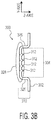
Figure 3A is a cross section of thecomponent carrier 300 in the x-z plane;Figure 3B is a cross section of thecomponent carrier 300 in the y-z plane; andFigure 3C - a top-view of thecomponent carrier 300 in the x-y plane. - Each
cavity 304 has a length 308 (x-axis), a height 310 (z-axis), a width (same as 304) (y-axis), and a set of cavity registration features 312. The cavity registration features 312 are separated from each other by a first cavity registration feature pitch 314 (y-axis) and a second cavity registration feature pitch 315 (x-axis). Thefirst pitch 314 andsecond pitch 315 can be the same or different, depending upon the components to be carried. - The single
continuous cavity 304 is further defined by a set of y-axis barriers 326 (e.g. sidewalls) and afloor region 328. The continuous cavity's 304 registration features 312 are configured to engage with a component's registration features. Since there are no barriers along the x-axis of thecontinuous cavity 304, components can be of different sizes and/or regularly or variably separated within thecarrier 300. In one example embodiment, sets of different electronic and/or mechanical components, perhaps with the same pitch, are capable of being placed in a same cavity 304 (e.g. reel). In such an example, a complete set of electronic and mechanical components, perhaps suitable for a certain application already pre-grouped in thecavity 304. -
Figures 3A ,3B and3C show an example embodiment where theindividual cavities 204 ofFigure 2 are replaced by thecontinuous cavity 304. Thecontinuous cavity 304 permits components of same or varying size to be spaced a regular or irregular intervals, thereby permitting flexibility of component size, carrying and/or placement in thecarrier 300. -
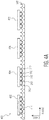
Figures 4A ,4B ,4C are an example 400 of the third example 300 of a component carrier paired with a set of components. -
Figure 4A is a cross section of thecomponent carrier 300 in the x-z plane filled with a set ofcomponents Figure 4B is a cross section of thecomponent carrier 300 in the y-z plane showing an edge of one of the components; andFigure 4C - a top-view of thecomponent carrier 300 in the x-y plane showing the set of components. In one example, thecomponents carrier 300 are overlaid by acover layer 410. - In this example embodiment,
Figure 4B shows that within the singlecontinuous cavity 304 thecomponents components - Similarly,
Figure 4A shows that within the singlecontinuous cavity 304 thecomponents components - The
continuous cavity 304 in some example embodiments, permitslower carrier 300 costs due to a reduction in a number ofcarriers 300 required to carry components of varying sizes and shapes. - The cavity registration features 312 encourages less movement of a product in the
carrier 300 and tends to reduce issues with chips or other products sticking in a barrier corner between a cover layer and a carrier substrate, thereby reducing damage to products and reducing customer concerns. -
Figures 5A, 5B, 5C are examples ofadditional component carriers various components Component carriers Component carrier 506 has a second set of cavity registration features 516. - Comparing the first and
second component carriers second component carrier 504 includes thecomponent 510 which has a depopulated bump layout (i.e. bumps are skipped). Note, dies can also be packaged using the same carrier layout. - One example discloses a component carrier, including: a cavity; wherein the cavity includes a set of cavity registration features configured to engage with a set of component registration features on a component; and wherein the cavity registration features are within the cavity.
- In other examples, components can have more bumps in one cavity, for various reasons like: some bumps have a different pitch from other bumps; component alignment in the carrier is done using one pitch on the component and/or in the registration features; other bumps are accommodated by leaving out some registration features (see second set of cavity registration features 516 in
Figure 5C having an aperiodic layout) if necessary; not all registration features may be needed; and/or different component bump types and/or dimensions are included on a single component. - In this specification, example embodiments have been presented in terms of a selected set of details. However, a person of ordinary skill in the art would understand that many other example embodiments may be practiced which include a different selected set of these details. It is intended that the following claims cover all possible example embodiments.
Claims (15)
- A component carrier, comprising:a cavity;wherein the cavity includes a set of cavity registration features configured to engage with a set of component registration features on a component; andwherein the cavity registration features are within the cavity.
- The carrier of claim 1:wherein the cavity includes a floor region; andwherein the set of cavity registration features are included in the floor region.
- The carrier of claim 1 or 2:wherein the set of cavity registration features are configured to position, orient or align a component within the cavity.
- The carrier of any preceding claim:wherein the set of cavity registration features have at least one of: a regular pitch, a variable pitch, or an aperiodic pitch.
- The carrier of any preceding claim:wherein the set of cavity registration features each have a same geometric shape.
- The carrier of any preceding claim:wherein the set of cavity registration features include a set of different geometric shapes.
- The carrier of any preceding claim:wherein the set of cavity registration features include at least one of: a topography, a protrusion, a hemisphere, a rectangle, a ridge, a circle, a polygon, a pillar, an arc, an egg-tray, or an interlocking feature.
- The carrier of any preceding claim:wherein the cavity is a continuous cavity configured to engage with the component registration features of more than one component.
- The carrier of claim 8:wherein the cavity is configured to variably separate the more than one component.
- The carrier of any preceding claim:wherein the cavity is one of a set of separate or individual cavities configured to engage with the component registration features of more than one component.
- The carrier of claim 9:wherein the set of separate cavities are separated by a set of barriers.
- The carrier of claim 9 or 11:wherein the set of separate or individual cavities are configured to regularly separate the more than one component.
- The carrier of any preceding claim:wherein the set of cavity registration features are thermally formed or embossed onto the carrier substrate.
- The carrier of any preceding claim:wherein the carrier substrate is at least one of: plastic, polyvinyl chloride, laminate, paper or metal.
- The carrier of any preceding claim:wherein the component carrier is configured to carry at least one of: an Integrated Circuit (IC) package, a chip, a die, a passive electronic component, an active electronic component, a microcontroller, a microprocessor, a module, a MEMS device, or a MOEMS device, a non-electronic device, or a micro-fluidic device.
Applications Claiming Priority (1)
| Application Number | Priority Date | Filing Date | Title |
|---|---|---|---|
| US15/352,214 US10315821B2 (en) | 2016-11-15 | 2016-11-15 | Component carrier |
Publications (1)
| Publication Number | Publication Date |
|---|---|
| EP3321956A1 true EP3321956A1 (en) | 2018-05-16 |
Family
ID=60301804
Family Applications (1)
| Application Number | Title | Priority Date | Filing Date |
|---|---|---|---|
| EP17200646.2A Withdrawn EP3321956A1 (en) | 2016-11-15 | 2017-11-08 | Component carrier |
Country Status (2)
| Country | Link |
|---|---|
| US (1) | US10315821B2 (en) |
| EP (1) | EP3321956A1 (en) |
Families Citing this family (3)
| Publication number | Priority date | Publication date | Assignee | Title |
|---|---|---|---|---|
| WO2020198426A1 (en) * | 2019-03-27 | 2020-10-01 | Daewon Semiconductor Packaging Industrial Company | Patterned carrier assemblies having an integrated adhesive film |
| JP2023102542A (en) * | 2022-01-12 | 2023-07-25 | 北越コーポレーション株式会社 | METHOD FOR MANUFACTURING CARRIER TAPE BASE FOR CHIP-TYPE ELECTRONICS |
| JPWO2023203955A1 (en) * | 2022-04-20 | 2023-10-26 |
Citations (5)
| Publication number | Priority date | Publication date | Assignee | Title |
|---|---|---|---|---|
| US5103976A (en) * | 1990-09-25 | 1992-04-14 | R. H. Murphy Company, Inc. | Tray for integrated circuits with supporting ribs |
| EP0570128A1 (en) * | 1992-05-13 | 1993-11-18 | GOLD INDUSTRIES Co. Ltd. | A linked container for transporting precision devices |
| US20010027933A1 (en) * | 1998-11-26 | 2001-10-11 | Keiichi Sasamura | Accommodation container, accommodation container for accommodating semiconductor devices and method of carrying semiconductor devices |
| US6505741B1 (en) * | 1999-05-21 | 2003-01-14 | Hirokazu Ono | Tray for receiving semiconductor devices |
| US20050073037A1 (en) * | 2003-10-02 | 2005-04-07 | Wright Lance C. | Method for securing a semiconductor device in a carrier tape |
Family Cites Families (3)
| Publication number | Priority date | Publication date | Assignee | Title |
|---|---|---|---|---|
| US4657137A (en) | 1981-05-22 | 1987-04-14 | North American Philips Corporation | Multi-chip packaging system |
| US4966282A (en) | 1989-01-13 | 1990-10-30 | Nitto Denko Corporation | Electronic component carrier |
| JP2002362623A (en) | 2001-06-08 | 2002-12-18 | Smk Corp | Packing tape member and packing method using packing tape member |
-
2016
- 2016-11-15 US US15/352,214 patent/US10315821B2/en active Active
-
2017
- 2017-11-08 EP EP17200646.2A patent/EP3321956A1/en not_active Withdrawn
Patent Citations (5)
| Publication number | Priority date | Publication date | Assignee | Title |
|---|---|---|---|---|
| US5103976A (en) * | 1990-09-25 | 1992-04-14 | R. H. Murphy Company, Inc. | Tray for integrated circuits with supporting ribs |
| EP0570128A1 (en) * | 1992-05-13 | 1993-11-18 | GOLD INDUSTRIES Co. Ltd. | A linked container for transporting precision devices |
| US20010027933A1 (en) * | 1998-11-26 | 2001-10-11 | Keiichi Sasamura | Accommodation container, accommodation container for accommodating semiconductor devices and method of carrying semiconductor devices |
| US6505741B1 (en) * | 1999-05-21 | 2003-01-14 | Hirokazu Ono | Tray for receiving semiconductor devices |
| US20050073037A1 (en) * | 2003-10-02 | 2005-04-07 | Wright Lance C. | Method for securing a semiconductor device in a carrier tape |
Also Published As
| Publication number | Publication date |
|---|---|
| US20180134473A1 (en) | 2018-05-17 |
| US10315821B2 (en) | 2019-06-11 |
Similar Documents
| Publication | Publication Date | Title |
|---|---|---|
| CN102709220B (en) | Semiconductor packages transfer equipment and utilize it to manufacture the method for semiconductor device | |
| EP3321956A1 (en) | Component carrier | |
| US7504315B2 (en) | Method of transporting semiconductor device and method of manufacturing semiconductor device | |
| US6981595B2 (en) | Carrier tape for electronic components | |
| US6857524B2 (en) | Tray for semiconductors | |
| US11764133B2 (en) | Tape carrier assemblies having an integrated adhesive film | |
| US9673124B2 (en) | Device and method for localized underfill | |
| KR100972587B1 (en) | Tray for Electronic Components | |
| US7257887B2 (en) | Die holding apparatus for bonding systems | |
| US8866281B2 (en) | Three-dimensional integrated circuits and fabrication thereof | |
| US20060157382A1 (en) | Electronic component package tape and method of manufacturing the same | |
| US7882957B2 (en) | Storing tray and storing device | |
| US8624376B1 (en) | Package-on-package structure without through assembly vias | |
| JP2003168731A (en) | Substrate tray, substrate tray laying sheet, and substrate storage method | |
| JP3856542B2 (en) | Carrier tape | |
| DE102016105787A1 (en) | A carrier tape having pockets comprising a base bottom portion and a raised bottom portion | |
| US7208346B2 (en) | Methods of forming interposers on surfaces of dies of a wafer | |
| KR20170022428A (en) | sputtering frame for semiconductor package and sputtering process using the same | |
| US20150115016A1 (en) | Ball mount module | |
| US6474476B1 (en) | Universal carrier tray | |
| JP7601595B2 (en) | Storage tray and method for manufacturing semiconductor chip package | |
| WO2021163651A1 (en) | Rigid carrier assemblies with tacky media molded thereon | |
| US9806064B2 (en) | Package with multiple plane I/O structure | |
| EP0571510B1 (en) | Packaging tape | |
| US20110018160A1 (en) | Method of Producing Covers for Electronics |
Legal Events
| Date | Code | Title | Description |
|---|---|---|---|
| PUAI | Public reference made under article 153(3) epc to a published international application that has entered the european phase |
Free format text: ORIGINAL CODE: 0009012 |
|
| STAA | Information on the status of an ep patent application or granted ep patent |
Free format text: STATUS: THE APPLICATION HAS BEEN PUBLISHED |
|
| AK | Designated contracting states |
Kind code of ref document: A1 Designated state(s): AL AT BE BG CH CY CZ DE DK EE ES FI FR GB GR HR HU IE IS IT LI LT LU LV MC MK MT NL NO PL PT RO RS SE SI SK SM TR |
|
| AX | Request for extension of the european patent |
Extension state: BA ME |
|
| STAA | Information on the status of an ep patent application or granted ep patent |
Free format text: STATUS: THE APPLICATION IS DEEMED TO BE WITHDRAWN |
|
| 18D | Application deemed to be withdrawn |
Effective date: 20181117 |