EP3321925A1 - Information processing device, display control program, and display control method - Google Patents
Information processing device, display control program, and display control method Download PDFInfo
- Publication number
- EP3321925A1 EP3321925A1 EP15898205.8A EP15898205A EP3321925A1 EP 3321925 A1 EP3321925 A1 EP 3321925A1 EP 15898205 A EP15898205 A EP 15898205A EP 3321925 A1 EP3321925 A1 EP 3321925A1
- Authority
- EP
- European Patent Office
- Prior art keywords
- display
- data transfer
- transfer rate
- resolution
- pbn
- Prior art date
- Legal status (The legal status is an assumption and is not a legal conclusion. Google has not performed a legal analysis and makes no representation as to the accuracy of the status listed.)
- Granted
Links
Images








Classifications
-
- G—PHYSICS
- G09—EDUCATION; CRYPTOGRAPHY; DISPLAY; ADVERTISING; SEALS
- G09G—ARRANGEMENTS OR CIRCUITS FOR CONTROL OF INDICATING DEVICES USING STATIC MEANS TO PRESENT VARIABLE INFORMATION
- G09G5/00—Control arrangements or circuits for visual indicators common to cathode-ray tube indicators and other visual indicators
- G09G5/003—Details of a display terminal, the details relating to the control arrangement of the display terminal and to the interfaces thereto
- G09G5/006—Details of the interface to the display terminal
-
- G—PHYSICS
- G06—COMPUTING OR CALCULATING; COUNTING
- G06F—ELECTRIC DIGITAL DATA PROCESSING
- G06F3/00—Input arrangements for transferring data to be processed into a form capable of being handled by the computer; Output arrangements for transferring data from processing unit to output unit, e.g. interface arrangements
- G06F3/14—Digital output to display device ; Cooperation and interconnection of the display device with other functional units
- G06F3/1423—Digital output to display device ; Cooperation and interconnection of the display device with other functional units controlling a plurality of local displays, e.g. CRT and flat panel display
-
- G—PHYSICS
- G06—COMPUTING OR CALCULATING; COUNTING
- G06F—ELECTRIC DIGITAL DATA PROCESSING
- G06F3/00—Input arrangements for transferring data to be processed into a form capable of being handled by the computer; Output arrangements for transferring data from processing unit to output unit, e.g. interface arrangements
- G06F3/14—Digital output to display device ; Cooperation and interconnection of the display device with other functional units
- G06F3/1423—Digital output to display device ; Cooperation and interconnection of the display device with other functional units controlling a plurality of local displays, e.g. CRT and flat panel display
- G06F3/1431—Digital output to display device ; Cooperation and interconnection of the display device with other functional units controlling a plurality of local displays, e.g. CRT and flat panel display using a single graphics controller
-
- G—PHYSICS
- G06—COMPUTING OR CALCULATING; COUNTING
- G06F—ELECTRIC DIGITAL DATA PROCESSING
- G06F3/00—Input arrangements for transferring data to be processed into a form capable of being handled by the computer; Output arrangements for transferring data from processing unit to output unit, e.g. interface arrangements
- G06F3/14—Digital output to display device ; Cooperation and interconnection of the display device with other functional units
-
- G—PHYSICS
- G09—EDUCATION; CRYPTOGRAPHY; DISPLAY; ADVERTISING; SEALS
- G09G—ARRANGEMENTS OR CIRCUITS FOR CONTROL OF INDICATING DEVICES USING STATIC MEANS TO PRESENT VARIABLE INFORMATION
- G09G2320/00—Control of display operating conditions
- G09G2320/06—Adjustment of display parameters
- G09G2320/0606—Manual adjustment
-
- G—PHYSICS
- G09—EDUCATION; CRYPTOGRAPHY; DISPLAY; ADVERTISING; SEALS
- G09G—ARRANGEMENTS OR CIRCUITS FOR CONTROL OF INDICATING DEVICES USING STATIC MEANS TO PRESENT VARIABLE INFORMATION
- G09G2340/00—Aspects of display data processing
- G09G2340/04—Changes in size, position or resolution of an image
- G09G2340/0407—Resolution change, inclusive of the use of different resolutions for different screen areas
-
- G—PHYSICS
- G09—EDUCATION; CRYPTOGRAPHY; DISPLAY; ADVERTISING; SEALS
- G09G—ARRANGEMENTS OR CIRCUITS FOR CONTROL OF INDICATING DEVICES USING STATIC MEANS TO PRESENT VARIABLE INFORMATION
- G09G2350/00—Solving problems of bandwidth in display systems
-
- G—PHYSICS
- G09—EDUCATION; CRYPTOGRAPHY; DISPLAY; ADVERTISING; SEALS
- G09G—ARRANGEMENTS OR CIRCUITS FOR CONTROL OF INDICATING DEVICES USING STATIC MEANS TO PRESENT VARIABLE INFORMATION
- G09G2352/00—Parallel handling of streams of display data
-
- G—PHYSICS
- G09—EDUCATION; CRYPTOGRAPHY; DISPLAY; ADVERTISING; SEALS
- G09G—ARRANGEMENTS OR CIRCUITS FOR CONTROL OF INDICATING DEVICES USING STATIC MEANS TO PRESENT VARIABLE INFORMATION
- G09G2354/00—Aspects of interface with display user
-
- G—PHYSICS
- G09—EDUCATION; CRYPTOGRAPHY; DISPLAY; ADVERTISING; SEALS
- G09G—ARRANGEMENTS OR CIRCUITS FOR CONTROL OF INDICATING DEVICES USING STATIC MEANS TO PRESENT VARIABLE INFORMATION
- G09G2360/00—Aspects of the architecture of display systems
- G09G2360/04—Display device controller operating with a plurality of display units
-
- G—PHYSICS
- G09—EDUCATION; CRYPTOGRAPHY; DISPLAY; ADVERTISING; SEALS
- G09G—ARRANGEMENTS OR CIRCUITS FOR CONTROL OF INDICATING DEVICES USING STATIC MEANS TO PRESENT VARIABLE INFORMATION
- G09G2370/00—Aspects of data communication
- G09G2370/04—Exchange of auxiliary data, i.e. other than image data, between monitor and graphics controller
- G09G2370/045—Exchange of auxiliary data, i.e. other than image data, between monitor and graphics controller using multiple communication channels, e.g. parallel and serial
-
- G—PHYSICS
- G09—EDUCATION; CRYPTOGRAPHY; DISPLAY; ADVERTISING; SEALS
- G09G—ARRANGEMENTS OR CIRCUITS FOR CONTROL OF INDICATING DEVICES USING STATIC MEANS TO PRESENT VARIABLE INFORMATION
- G09G2370/00—Aspects of data communication
- G09G2370/10—Use of a protocol of communication by packets in interfaces along the display data pipeline
-
- G—PHYSICS
- G09—EDUCATION; CRYPTOGRAPHY; DISPLAY; ADVERTISING; SEALS
- G09G—ARRANGEMENTS OR CIRCUITS FOR CONTROL OF INDICATING DEVICES USING STATIC MEANS TO PRESENT VARIABLE INFORMATION
- G09G2370/00—Aspects of data communication
- G09G2370/22—Detection of presence or absence of input display information or of connection or disconnection of a corresponding information source
Definitions
- the embodiments discussed herein relate to an information processing device, a display control program, and a display control method.
- a multi-display setup is known.
- a PC Personal Computer
- a PC equipped with single connector and a branch device connected to the connector of the PC are used.
- the branch device splits the display data of multiple streams, and transmits the splitted data to each display device respectively.
- Multi-Stream Transport hereinafter referred to as "MST” supported by DisplayPort 1.2a (hereinafter represented as "DP1.2a"
- DP1.2a DisplayPort 1.2a
- Patent Document 1 Japanese Laid-Open Patent Publication No. 2010-160304 .
- the PC transmits display data of multiple streams to each display device connected to the branch device by splitting the display data
- the PC transmits the display data of multiple streams by sharing a certain bandwidth.
- available data transfer rates of other display devices also vary. Since a displayable resolution of each display depends on a data transfer rate, a range of displayable resolutions of each display varies in accordance with a change of a data transfer rate. But it is difficult for users to recognize a range of displayable resolutions of each display varying in accordance with a change of a data transfer rate.
- a user when a user cannot set a certain resolution to a display device, it is difficult for the user to identify a cause whether the certain resolution exceeds a range of resolutions supported by a PC, or the certain resolution exceeds an upper limit of a resolution at which the display device can display.
- the certain resolution cannot be set to the display device, the user sometimes makes inquiries to a vendor, makes a complaint to the vendor that a resolution cannot be set, or requests repair or return of the PC.
- one of the purposes of one aspect of the present disclosure is to enable a user to determine a displayable resolution of a display device connected to an information processing device via a function expansion unit.
- an information processing device capable of connecting to a display device using a function expansion unit.
- the information processing device includes: a calculation unit configured to calculate, from a resolution to be used in the display device, a data transfer rate of the display device; and a display controlling unit configured to display, based on a data transfer rate at a given resolution calculated by the calculation unit, a ratio of the data transfer rate of the display device to an allowable data transfer rate, so as to be visibly recognized.
- the information processing device capable of connecting to a display device using a function expansion unit.
- the information processing device includes: a calculation unit configured to calculate, from a resolution to be used in the display device, a data transfer rate of the display device; and a display controlling unit configured to display, based on a data transfer rate at a given resolution calculated by the calculation unit, a ratio of the data transfer rate of the display device to an allowable data transfer rate, so as to be visibly recognized.
- a technique can be provided that enables a user to easily determine a displayable resolution of a display device connected to an information processing device via a function expansion unit.
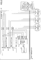
- FIG. 1 is a diagram illustrating a display system according to the present embodiment.
- the display system displays information on the multiple display devices (hereinafter referred to as "displays") connected to an information processing device.
- an information processing device is a personal computer (PC).
- the information processing device is not necessarily a PC, and other devices such as a tablet device may be used as the information processing device.
- MST which is a mode supported in DP 1.2a standardized by VESA
- a Source Device a Branch Device, and a Sink Device are defined.
- a PC main unit 10 corresponds to the Source Device.
- a function expansion unit, which is docked to the PC main unit 10, is an example of the Branch Device (branch device 20).
- the function expansion unit may be an external port replicator connected to the PC main unit 10, or may be embedded with the PC main unit 10.
- An example of the Sink Device is a display connected to the branch device 20.
- a first display 31, a second display 32, and a third display 33 are illustrated, all of which are connected to the branch device 20.
- a fourth display 34 is directly connected to an output port 12 of a graphic chip 11 inside the PC main unit 10.
- the first display 31, the second display 32, and the third display 33 are connected to an output port 13 of the graphic chip 11 via the branch device 20.
- main link signal lines are used for transmitting display data to be displayed on the display.
- a data transfer rate of the main link is 5.4 Gbps (Gigabits per second) per lane.
- the fourth display 34 is not affected by the data transfer rates of the first, second, or third displays (31, 32, or 33), and can use a bandwidth of 21.6 Gbps for transferring display data.
- each of the first, second, and third displays (31 to 33) needs to be configured such that a sum of data transfer rates of the first to third displays (31 to 33) does not exceed 21.6 Gbps.
- a data transfer rate corresponds to an available frequency when transferring display data.
- PBN which will be described later represents a peak bandwidth obtained by normalizing data transfer rate. That is, a value represented by PBN is proportional to data transfer rate.
- An HPD signal line is used for sending and receiving a signal indicating whether a display is connected or not. When an HPD signal is changed from Low to High, it means that the corresponding display was connected. When an HPD signal is Low, it means that the corresponding display is not connected.
- An AUX signal line is used for sending and receiving control signals concerning communication between the graphic chip 11 and a display.
- the PC main unit 10 is equipped with a microcontroller 15.
- the microcontroller 15 is connected to both the AUX signal lines associated with the output ports 12 and 13 respectively and to both the HPD signal lines associated with the output ports 12 and 13 respectively, so that the AUX signals and the HPD signals associated with the output ports 12 and 13 can be entered.
- the microcontroller 15 monitors (performs snooping) communications between the graphic chip 11 and each display by using both the AUX signal line connected to the output port 12 and the AUX signal line connected to the output port 13, to obtain EDID (Extended Display Identification Data) information from the first display 31 to the fourth display 34.
- the microcontroller 15 can use a conventional method to perform snooping of the AUX signal.
- the EDID information includes display information of a screen such as a resolution.
- the microcontroller 15 further obtains DPCD (Display Port Configuration Data) information which is retained in the branch device 20 and each display.
- the DPCD information includes information about data transfer, such as a data transfer rate and the number of lanes.
- the DPCD information retained in the branch device 20 includes data transfer rate between the branch device 20 and the graphic chip 11.
- the DPCD information retained in each display includes a data transfer rate between the branch device 20 and each display.
- the graphic chip 11 is triggered with a change of the HPD signal from Low into High to start communication with the connected display.
- the microcontroller 15 obtains the EDID information transmitted from the connected display to the graphic chip 11, and stores the EDID information into an internal memory of the microcontroller 15.
- the microcontroller 15 obtains the DPCD information, and stores the DPCD information into the internal memory of the microcontroller 15.
- the microcontroller 15 may obtain the DPCD information (data transfer rate) retained in the branch device 20 via the AUX signal line before the display is connected, and store the DPCD information into the internal memory.
- the microcontroller 15 may obtain the DPCD information retained in each display after each of the display is connected, and store the DPCD information into the internal memory.
- a configurable resolution display application which will be described later, reads the EDID information and the DPCD information stored in the internal memory of the microcontroller 15 via I2C (I-squared-C), by using a GPIO pin 16.
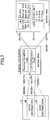
- a first display 31 is connected to an output port 12 of a graphic chip 11.
- a second display 32 is connected to an output port 13 of the graphic chip 11.
- a third display 33 is connected to an output port 14 of the graphic chip 11.
- each of the first display 31 to the third display 33 may be configured independently such that a data transfer rate of each display does not exceed 21.6 Gbps. In this case, a user can easily predict at what resolution each display can display.
- the first to third displays (31 to 33) need to be configured such that a sum of data transfer rates of the first to third displays (31 to 33) does not exceed 21.6 Gbps.
- configurable resolution ranges of each of the first display 31 to the third display 33 vary depending on the resolutions of other displays. Accordingly, the information processing device according to the present embodiment displays configurable resolution ranges of each of multiple displays connected to the branch device 20 in a visible manner.
- the microcontroller 15 includes a processor 151 and an internal memory 152.
- the processor 151 obtains the DPCD information by snooping into the AUX signal, thereby to obtain the data transfer rate and the number of the lanes (4 lanes in the present embodiment).
- a data transfer rate per lane is 5.4 Gbps
- data transfer at 21.6 Gbps can be attained using 4 lanes.
- a data transfer rate per lane is 2.7 Gbps
- data transfer at 10.8 Gbps can be attained using 4 lanes.
- the processor 151 also obtains the EDID information to obtain information concerning display setting of a display, such as a resolution and the like.
- the internal memory 152 stores the EDID information and the DPCD information.
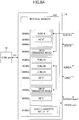
- the microcontroller 15 includes an acquisition unit 153, a calculation unit 154, a conversion unit 155, a memory unit 156, a setting unit 157, and a display controlling unit 158.
- the acquisition unit 153 acquires the DPCD information and the EDID information.
- the calculation unit 154 calculates a data transfer rate from a resolution used by a display.
- the conversion unit 155 converts a resolution into a pixel clock frequency by using a conversion table 40 of VESA standard, for example.
- the memory unit 156 stores the conversion table 40, EDID information 50, and DPCD information 60.
- the memory unit 156 may store a program for the configurable resolution display application.
- the setting unit 157 sets a resolution of a display.
- the display controlling unit 158 displays, based on a data transfer rate calculated from the certain resolution, a ratio of the data transfer rate to be used to an allowable data transfer rate, so as to be visibly recognized.
- the functions of the acquisition unit 153, the calculation unit 154, the conversion unit 155, the setting unit 157, and the display controlling unit 158 can be embodied by the processor. Also, the function of the memory unit 156 can be embodied by the internal memory 152.
- FIG. 5 illustrates an example of the conversion table 40 according to the present embodiment.
- the conversion table 40 stores a resolution (display resolution) 41, a refresh rate 42, and a pixel clock frequency 43, each of which is correlated with each other.
- the conversion unit 155 can convert a set of the resolution 41 and the refresh rate 42 into the pixel clock frequency 43.
- the conversion unit 155 may perform conversion from only the resolution 41 into the pixel clock frequency 43.
- RB Reduced Blanking
- CRT Timing a display timing which does not reduce a blanking interval
- FIG. 6 illustrates an example of the EDID information 50 according to the present embodiment.
- the EDID information 50 according to VESA standard includes information about displayable resolutions of a display. If a display supports Reduced Blanking timing, a pixel clock frequency is necessarily stored in one of Detailed Timings located in address ranges from 36h to 7Dh. When information of the same resolution is stored in the Detailed Timing and the Standard Timing of the conversion table 40, or in the Detailed Timing and the Established Timing of the conversion table 40, the pixel clock frequency in the Detailed Timing (corresponding to Reduced Blanking) is applied. As for a resolution which is stored only in the Standard Timing or Established Timing, the pixel clock frequency corresponding to CRT timing is applied.
- FIG. 7 illustrates an example of a storage region of the DPCD information 60 according to the present embodiment.
- the DPCD information 60 and the EDID information 50 are stored in the internal memory 15. Addresses from 00000h to 000FFh are Receiver Capability Field, and addresses from 00100h to 001FFh are Link Configuration Field.
- the Link Configuration Field contained in addresses from 00100h to 001FFh of the internal memory 15 stores a data transfer rate. Further, at addresses from 00101h to 00102h, the number of lanes (Lane Count) is stored.
- FIG. 8A and FIG. 8B Examples of data stored in the internal memory 152 of the microcontroller according to the present embodiment are illustrated in FIG. 8A and FIG. 8B .
- FIG. 8A illustrates an example of data stored in the internal memory 152 when the display system is configured such that the branch device 20 is used, as illustrated in FIG. 1 .
- FIG. 8B illustrates an example of data stored in the internal memory 152 when the display system is configured such that the branch device 20 is not used, as illustrated in FIG. 2 .
- information about the fourth display is stored from addresses 00000h to 01000h.
- Information about the fourth display includes the EDID information (EDID_4) and the DPCD (data transfer rate) of the fourth display. Note that an address (or address range) where "All "0"" is written represents that no data is stored in the address (or address range).
- information about the first, second, and third display is stored.
- the EDID information of the first, second, and third displays EDID_21, EDID_22, and EDID_23
- the DPCD data transfer rate
- Presence or absence of the branch device 20, and the number of displays connected to the branch device 20 can be identified by the EDID information obtained from the corresponding AUX signal line.
- the number of the EDID information stored in the internal memory 152 obtained via the AUX signal line is 1, it means that the branch device 20 does not exist.
- the number of the EDID information is more than 1, it means that as many displays as the number of the EDID information are connected to the branch device 20.
- the example of the internal memory 152 illustrated in FIG. 8A represents that the branch device 20 exists and three displays are connected to the branch device 20.
- the example of the internal memory 152 illustrated in FIG. 8A also represents that a display (which is not connected to the branch device 20) is connected to a port independent of other displays.
- the example of the internal memory 152 illustrated in FIG. 8B represents that the branch device 20 does not exist and that three displays are respectively connected to ports independently. Note that contents of the internal memory 152 are updated for every access from the graphic chip 11.
- whether the displays are independently connected or connected via the branch device 20 can be identified based on the number of the EDID information stored in the predetermined addresses of the internal memory 152. Also, based on the DPCD information stored in the predetermined addresses of the internal memory 152, data transfer rate can be identified.
- FIGS. 9 and 10 Before describing the configurable resolution display processing, an example of a resolution setting processing for the display system illustrated in FIG. 2 will be explained, with reference to FIGS. 9 and 10 .
- the configurable resolution display processing according to the present embodiment performed by, for example, the display system illustrated in FIG. 1 , will be explained with reference to FIGS. 11 to 14 .
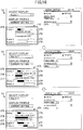
- FIGS. 15 to 17 examples of contents displayed on a screen by performing the configurable resolution display processing according to the present embodiment will be described.
- the display system illustrated in FIG. 2 does not include a branch device 20, and each of the first display 31, the second display 32, and the third display 33 is connected to the graphic chip 11 directly.
- the processor 151 first detects the number of displays connected to the PC main unit 10 (step S10) (in the following description, the number is referred to as "n"). In the example illustrated in FIG. 2 , n is 3.
- the processor 151 sets a variable i to 1 (step S12).
- the variable i represents a type of an identification number of the display currently connected.
- the processor 151 identifies a displayable resolution of the first display (step S16).
- the processor 151 determines whether the variable i is less than (n+1) (step S18).
- the processor 151 add 1 to the variable i (step S20), and the processing reverts to step S14.
- the processor 151 repeats the steps S14 to S20 until the variable i becomes not less than (n+1) at step S18.
- step S22 A user selects, among the selectable displays (first, second, and third displays) which is displayed on the screen, one display. In the following description, a case in which the user selects the first display will be described.
- the processor 151 selects the first display (step S22).
- the processor 151 sets a variable j to 1 (step S24).
- the variable j represents a display number of a display whose resolution is being set. What is described here is a case, in which a number "1" of the first display selected by the user is set to the variable j.
- step S26 the processor 151 executes a resolution setting routine for display j which will be described later (step S26).
- the processor 151 determines whether the variable j is less than (n+1) (step S28).
- the processor 151 adds 1 to the variable j (step S30), and the processing reverts to step S26.
- the processor 151 repeats the steps S26 to S30 until the variable j becomes not less than (n+1) at step S28.
- the processor 151 decides that the setting of the displays completed and terminates the processing.
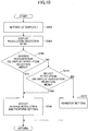
- the resolution setting routine which is called at step S26 in FIG. 9 will be described with reference to a flowchart illustrated in FIG. 10 .
- the processor 151 selects display j (here, the first display is selected) (step S262).
- the processor 151 displays a resolution selection menu (step S264).
- the processor 151 determines whether a desired resolution is displayed on the resolution selection menu or not (step S266). If it is determined that the desired resolution is displayed on the resolution selection menu, the processor 151 select the desired resolution in accordance with an operation of the user, sets the resolution of the first display to the selected resolution (step S268), and terminates the routine.
- the resolution of the first display is set to 1920 ⁇ 1080 60 Hz 24 bpp, for example.
- the processor 151 determines whether the display is set to one of the resolutions existing in the resolution selection menu in accordance with an operation of the user (step S270). If it is determined that the display is set to one of the resolutions existing in the resolution selection menu in accordance with an operation of the user, the processor 151 selects the resolution from the resolution selection menu, sets the selected resolution to the first display (step S268), and terminates the routine. If it is determined that the display is not set to one of the resolutions existing in the resolution selection menu at step S270, the processor 151 abandons setting a resolution of the first display (step S272), and terminates the routine.
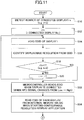
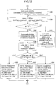
- FIGS. 11 to 13 are a set of flowcharts illustrating an example of a process flow of the configurable resolution display processing according to the present embodiment.
- FIG. 14 is a flowchart illustrating an example of a process flow of a resolution setting routine according to the present embodiment.
- the acquisition unit 153 in the processor 151 performs steps S10 through S20. Since these steps are the same as the steps S10 through S20 illustrated in FIG. 9 and are already explained, the description of these steps is omitted.
- the acquisition unit 153 reads the EDID information retained in a display in response to a change of the HPD signal which changes from Low to High when the display is connected (step S32).
- the acquisition unit 153 reads EDID information of each display from the internal memory 152 via I2C (step S34). After step S34, the processing proceeds to "1" in FIG. 12 ).
- the acquisition unit 153 sets AddressE to 00000h, to designate a storage region for the EDID information in the internal memory 152 (step S36).
- the acquisition unit 153 obtains data stored in an address range from AddressE to (AddressE+000FFh) as the EDID information (step S38).
- the EDID information 50 stored in the "Receiver Capability Field" in the internal memory 15 illustrated in FIG. 7 is obtained.
- the acquisition unit 153 determines whether the designated region is "All "0"" (no information is stored) or not (step S40). If it is determined that the designated region is not "All "0”", the acquisition unit 153 adds a variable n to 1, and adds the AddressE to 100h, to designate a storage region for the EDID information of the second display connected to the branch device 20 (step S42). The acquisition unit 153 again performs step S38 to obtain data stored in an address range from AddressE to (AddressE+000FFh) as the EDID information of the second display (step S38).
- Steps S38 to S42 are repeatedly executed until it is determined that the designated region is "All "0"" at step S40. By repeating these steps, the EDID information of the first to third displays is obtained.
- the acquisition unit 153 sets AddressD to 01000h to designate a storage region for the DPCD information in the internal memory 152 (step S44).
- the acquisition unit 153 obtains a part of the DPCD information stored in an address of AddressD+00100h, and stores the information to LINK_BW (step S46).
- the DPCD information stored in the "Link Configuration Field" in the internal memory 152 illustrated in FIG. 7 is obtained.
- the value stored in the LINK BW is 06h, it means that the data transfer rate is 1.62 Gbps.
- the value is 0Ah, it means that the data transfer rate is 2.7 Gbps.
- the value is 14h it means that the data transfer rate is 5.4 Gbps.
- the usable data transfer rate is expressed in units of PBNs (Payload Bandwidth Numbers).
- PBNs Payment Bandwidth Numbers
- One unit of PBN is 54/64 (Mbytes/sec).
- the display controlling unit 158 displays a bar graph representing the total data transfer rate in green.
- Displayable total pixel rate is determined in advance, and a maximum total data transfer rate corresponding to the total pixel rate is 21.6 Gbps when using MST in DP 1.2a.
- the data transfer rate of 21.6 Gbps regulated in DP 1.2a is in an unused state. Accordingly, since a usable data transfer rate at this point of time is 2560 PBN, which is a maximum data transfer rate, the display controlling unit 158 displays a bar graph representing the total data transfer rate of 2560 PBN in green.
- a bar graph 171 representing the total data transfer rate of 2560 PBN is displayed in green (note: in the drawings, a white box is used instead of green).
- a red (black is used in the drawings instead of red) portion 172 is illustrated in FIG. 15 , the portion 172 is not displayed in red color and is displayed in green when step S56 is executed.
- the acquisition unit 153 sets a variable i to 1 (step S58).
- the calculation unit 154 identifies a displayable resolution of the first display from the EDID information (step S62). Next, the calculation unit 154 converts the displayable resolution into a pixel clock frequency based on the conversion table 40 to identify a maximum displayable frequency (x MHz) of the first display (step S64).
- the calculation unit 154 calculates a data transfer rate to be used by the first display Y(1) PBN, based on a formula (1) described below (step S66). Since the data transfer rate is calculated by adding a margin of 0.6 %, a maximum data transfer rate (PBN) representing a bandwidth to be used is obtained by multiplying an actual data transfer rate (PBN) by 1.06.
- PBN maximum data transfer rate
- the display controlling unit 158 displays a bar graph representing the calculated individual data transfer rate Y(1) PBN having a length of "559.7 PBN" in green (step S68).
- step S68 By performing step S68, in a PBN display region 170 in the screen "a" illustrated in FIG. 15 , for example, a bar graph 173 representing the maximum data transfer rate of the first display having a length of 559.7 PBN is displayed in green. Though a red (black) portion 174 is illustrated in FIG. 15 , the portion 174 is not displayed in red color and is displayed in green when step S68 is executed.
- the acquisition unit 153 determines whether the variable i is less than (n+1) (step S70).
- the processor 151 adds 1 to the variable i (step S72), and the processing reverts to step S60.
- the processor 151 repeats steps S60 to S68 until the variable i becomes not less than 4. By repeating the steps, maximum data transfer rates of the second and the third displays are identified.
- the conversion unit 155 obtains, based on the conversion table 40, the pixel clock frequency corresponding to the resolution as "268.5 MHz", by converting "2560 ⁇ 1600 60 Hz (RB)".
- the display controlling unit 158 displays a bar graph representing the calculated individual data transfer rate of the second display Y(2) PBN having a length of "1011.9 PBN" in green (step S68).
- a bar graph 175 representing the maximum data transfer rate of the second display having a length of 1011.9 PBN is displayed in green.
- a bar graph 176 representing the maximum data transfer rate of the third display having a length of 988.4 PBN is displayed in green.
- a maximum displayable resolution turns out to be 1920 ⁇ 1440 60 Hz (234 MHz), based on the conversion table 40. Therefore, it is determined that a resolution of "1920 ⁇ 1440 60 Hz" or less can be used for the third display.
- the calculation unit 154 selects the first display in accordance with the user's operation (step S74).
- the setting unit 157 determines whether the variable j is less than 4 and the usable data transfer rate z is not less than the data transfer rate A (step S82). If it is determined that the variable j is less than 4 and the data transfer rate z is not less than the data transfer rate A, the setting unit 157 adds j to 1 (step S84), and performs step S80 again. If it is determined that the variable j is not more than 4 or the data transfer rate z is less than the data transfer rate A, the setting unit 157 determines that resolution changes of displays are completed, and terminates the processing.
- the resolution setting routine which is called at step S80 in FIG. 13 will be described with reference to a flowchart illustrated in FIG. 14 .
- the setting unit 157 selects a display j (step S802).
- the display controlling unit 158 displays a resolution selection menu (step S804).
- the setting unit 157 determines whether a desired resolution is displayed on the resolution selection menu or not (step S806). If it is determined that the desired resolution for the display j is displayed on the resolution selection menu, the calculation unit 154 selects the desired resolution for the display j in accordance with the user's operation (step S808).
- the calculation unit 154 converts the resolution into a pixel clock frequency (which will be referred to as "x MHz") based on the conversion table 40 (step S810).
- a resolution of "1920 ⁇ 1080 60 Hz 24 bpp" is selected from the resolution selection menu
- the calculation unit 154 converts the above resolution into a pixel clock frequency of "148.5 MHz” based on the conversion table 40.
- the calculation unit 154 calculates a data transfer rate Y(1) PBN by substituting "148.5 MHz” in the above formula (1).
- the data transfer rate Y(1) PBN will be "559.7 PBN”.
- the calculation unit 154 calculates a residual usable data transfer rate z.
- the display controlling unit 158 changes color of a portion of the bar graph representing the total data transfer rate. Specifically, in the bar graph, the portion extending from the left end to a position corresponding to the data transfer rate Y(j) is displayed in red, and the rest of the bar graph corresponding to the residual data transfer rate z is displayed in green (step S812). Next, the display controlling unit 158 changes color of a portion of the bar graph representing the data transfer rate of the first display. Specifically, in the bar graph, the portion extending from the left end to a position corresponding to the data transfer rate Y(j) is displayed in red, and the rest of the bar graph is displayed in green (step S814). After step S814, the processing terminates.
- step S806 it is determined that the desired resolution is displayed on the resolution selection menu
- the setting unit 157 determines whether a resolution existing in the resolution selection menu is set (step S810). If it is determined that a resolution existing in the resolution selection menu is set, the calculation unit 154 selects the resolution in accordance with the user's operation (step S818). After executing steps S810 to S814, the processing terminates.
- a resolution of "1280 ⁇ 1280 60 Hz 24 bpp" is selected, at steps S812 to S814, a pixel clock frequency corresponding to the selected resolution and a data transfer rate Y(j) PBN are calculated, and the color of a portion of the bar graph corresponding to the data transfer rate in use is changed to red (steps S812, S814).
- step S810 determines whether a resolution existing in the resolution selection menu is not set. If, at step S810, it is determined that a resolution existing in the resolution selection menu is not set, the setting unit 157 determines whether the variable is not less than 2 (step S816) . If it is determined that j is less than 2, the setting unit 157 suspends the resolution setting (step S820). If it is determined that j is not less than 2, the setting unit 157 subtracts 2 from the variable j, and the processing reverts to the previous display setting (step S818).
- the setting unit 157 determines, at step S82, that the variable j is less than 4 and the residual data transfer rate z (2033 PBN) is not less than a data transfer rate A used by the first display (245 PBN).
- the setting unit 157 adds j to 1 (step S84), and executes step S80 again to perform a resolution setting process of the second display.
- the display controlling unit 158 displays a bar graph representing the data transfer rate of the second display, such that a left end of a portion 177, corresponding to the data transfer rate Y(2) displayed in red, is aligned with a right end of a portion 174 of the bar graph representing the data transfer rate of the first display, corresponding to the data transfer rate Y(1) displayed in red.
- step S82 in FIG. 13 the variable j is less than 4 and the residual data transfer rate z (988 PBN) is not less than the data transfer rate A used by the second display (245 PBN).
- the setting unit 157 adds 1 to the variable j (step S84), and executes step S80 again to perform a resolution setting process of the third display.
- the display controlling unit 158 displays a bar graph representing the data transfer rate of the third display, such that a left end of a portion 178, corresponding to the data transfer rate Y(3) displayed in red, is aligned with a right end of a portion 177 of the bar graph representing the data transfer rate of the second display, corresponding to the data transfer rate Y(2) displayed in red.
- the display controlling unit 158 displays the portion 178 corresponding to the data transfer rate Y(3) in red, and terminates the processing.
- the display system in the present embodiment including multiple displays can calculate data transfer rates to be used for the multiple displays respectively, calculate a ratio of a sum of the data transfer rates to the maximum data transfer rate of 21.64 Gbps, and display the ratio and the maximum data transfer rate in different colors. Since a data transfer rate is in proportion to a display resolution, a user can easily identify a displayable resolution of each display by looking at a graph representing a usage of a data transfer rate displayed in colors.
- the display control method according to the present embodiment can be embodied by adding the configurable resolution display application and the microcontroller to obtain and maintain the EDID information and the DPCD information. Therefore, since modification of drivers or OS is not required, the display system according to the present embodiment can be easily provided.
- step S804 the display controlling unit 158 does not need to display the resolution selection menu when the residual data transfer rate z is less than a predetermined threshold.
- FIG. 16 illustrates an example of a display screen used in a display system in which a first display is connected to a PC main unit 10 independently of a second display and a third display, and the second display and the third display are connected to the PC main unit 10 via a branch device 20.
- a data transfer rate of the first display is expressed as a bar graph independent of other graphs, which includes a red portion 272 and a green portion 271.
- how much percent of the allowable data transfer rate (displayable resolution) of the first display is in use can be displayed visibly.
- a bar graph 273 representing a total allowable data transfer rate, and individual graphs 274 and 275 each representing a data transfer rate of the second display and a data transfer rate of the third display are displayed.
- a screen "b" or "c" of FIG. 16 by displaying red bars 272, 276, and 277, and green bars 271, 274, and 275, allowable data transfer rates of the second display and the third display can be displayed visibly.
- FIG. 17 illustrates an example of a display screen used in a display system in which a first, a second, and a third displays are connected to a PC main unit 10 independently of each other.
- a red bar graph 372 and a green bar graph 371 are displayed for representing a data transfer rate of the first display
- a red bar graph 373 is displayed for representing a data transfer rate of the second display
- a red bar graph 375 and a green bar graph 374 are displayed for representing a data transfer rate of the third display.
- the display system according to the present embodiment displays, when displaying a graph representing the total data transfer rate, how much percent of a total allowable data transfer rate (displayable resolution) is currently being used in a certain color (for example, in red), and displays a residual data transfer rate in a different color (for example, green).
- the display system according to the present embodiment also displays individual graphs respectively corresponding to each display juxtaposed with the graph representing the total data transfer rate, and displays in the individual graphs to what extent data transfer rates are used when resolution settings are performed.
- the display system according to the present embodiment can display residual data transfer rates of each display visibly.
- the information processing system, the display control program, and the display control method are described in the above embodiment.
- the information processing system, the display control program, and the display control method according to the present invention are not limited to the embodiment described above.
- Various modifications or enhancement can be applied within the scope of the present invention. Further, multiple embodiments or modified examples can be combined as long as inconsistencies do not occur in the combination.
- the display system according to the present embodiment may be controlled by software instead of the microcontroller in the PC main unit 10.
- an interface for the software obtaining the AUX signal and the HPD signal is required in the display system.
- an application program configured to cause a CPU of the PC main unit 10 to perform the same functions as the functions which are embodied by the microcontroller in the embodiment described above based on the AUX signal or HPD signal, and by executing the application program by the CPU of the PC main unit 10, the configurable resolution display processing according to the present disclosure can be performed without requiring the microcontroller.
Landscapes
- Engineering & Computer Science (AREA)
- Theoretical Computer Science (AREA)
- Physics & Mathematics (AREA)
- General Physics & Mathematics (AREA)
- Human Computer Interaction (AREA)
- General Engineering & Computer Science (AREA)
- Computer Hardware Design (AREA)
- Computer Graphics (AREA)
- Controls And Circuits For Display Device (AREA)
- Digital Computer Display Output (AREA)
Abstract
Description
- The embodiments discussed herein relate to an information processing device, a display control program, and a display control method.
- In recent years, high resolution and high quality of images are displayed in a display device. For example, there is known a technique capable of achieving a high quality image display independent of a transfer capacity of a transfer means for transferring display data (see Japanese Laid-Open Patent Publication No.
2010-160304 - Further, a multi-display setup is known. There are mainly two types of methods for a multi-display setup. In the first method, a PC (Personal Computer) is equipped with multiple connectors, and by connecting display devices to each connector, a multi-display setup is attained. In the second method, a PC equipped with single connector and a branch device connected to the connector of the PC are used. By connecting multiple display devices to the PC via the branch device, a multi-display setup is attained. In the second method, when the PC outputs display data of multiple streams, the branch device splits the display data of multiple streams, and transmits the splitted data to each display device respectively. Multi-Stream Transport (hereinafter referred to as "MST") supported by DisplayPort 1.2a (hereinafter represented as "DP1.2a") standardized by VESA is one of the specifications for implementing the second method.
- [Patent Document 1] Japanese Laid-Open Patent Publication No.
2010-160304 - However, when the PC transmits display data of multiple streams to each display device connected to the branch device by splitting the display data, the PC transmits the display data of multiple streams by sharing a certain bandwidth. Thus, when a data transfer rate for transmitting to one of the display devices varies, available data transfer rates of other display devices also vary. Since a displayable resolution of each display depends on a data transfer rate, a range of displayable resolutions of each display varies in accordance with a change of a data transfer rate. But it is difficult for users to recognize a range of displayable resolutions of each display varying in accordance with a change of a data transfer rate.
- Especially, since the number of types of displayable resolutions and the number of display devices increase in VESA standard, the number of combinations of resolutions which can be set to each display device becomes very large, and which thereby makes it more difficult for users to recognize displayable resolutions of each display device.
- Further, when a user cannot set a certain resolution to a display device, it is difficult for the user to identify a cause whether the certain resolution exceeds a range of resolutions supported by a PC, or the certain resolution exceeds an upper limit of a resolution at which the display device can display. When the certain resolution cannot be set to the display device, the user sometimes makes inquiries to a vendor, makes a complaint to the vendor that a resolution cannot be set, or requests repair or return of the PC.
- Accordingly, one of the purposes of one aspect of the present disclosure is to enable a user to determine a displayable resolution of a display device connected to an information processing device via a function expansion unit.
- According to an aspect of the embodiments, there is provision for an information processing device capable of connecting to a display device using a function expansion unit. The information processing device includes: a calculation unit configured to calculate, from a resolution to be used in the display device, a data transfer rate of the display device; and a display controlling unit configured to display, based on a data transfer rate at a given resolution calculated by the calculation unit, a ratio of the data transfer rate of the display device to an allowable data transfer rate, so as to be visibly recognized.
- There is provision of an information processing device capable of connecting to a display device using a function expansion unit. The information processing device includes: a calculation unit configured to calculate, from a resolution to be used in the display device, a data transfer rate of the display device; and a display controlling unit configured to display, based on a data transfer rate at a given resolution calculated by the calculation unit, a ratio of the data transfer rate of the display device to an allowable data transfer rate, so as to be visibly recognized.
- According to one aspect of the present disclosure, a technique can be provided that enables a user to easily determine a displayable resolution of a display device connected to an information processing device via a function expansion unit.
-
-
FIG. 1 is a diagram illustrating an overall configuration of a display system according to an embodiment; -
FIG. 2 is another diagram illustrating an overall configuration of a display system; -
FIG. 3 is a diagram illustrating a hardware configuration of a microcontroller according to the embodiment; -
FIG. 4 is a diagram illustrating a functional configuration of the microcontroller according to the embodiment; -
FIG. 5 illustrates an example of a conversion table according to the embodiment; -
FIG. 6 illustrates an example of EDID information according to the embodiment; -
FIG. 7 illustrates an example of DPCD information according to the embodiment; -
FIG. 8A illustrates an example of data stored in an internal memory of the microcontroller according to the embodiment; -
FIG. 8B illustrates an example of data stored in an internal memory of the microcontroller according to the embodiment; -
FIG. 9 is a flowchart describing an example of a resolution setting processing; -
FIG. 10 is a flowchart describing an example of a resolution setting routine; -
FIG. 11 is a flowchart illustrating an example of a process flow of the configurable resolution display processing according to the embodiment; -
FIG. 12 is a flowchart illustrating an example of a process flow of the configurable resolution display processing according to the embodiment; -
FIG. 13 is a flowchart illustrating an example of a process flow of the configurable resolution display processing according to the embodiment; -
FIG. 14 is a flowchart describing an example of a resolution setting routine according to the embodiment; -
FIG. 15 is a view illustrating an example of a display screen according to the embodiment; -
FIG. 16 is a view illustrating an example of a display screen according to the embodiment; and -
FIG. 17 is a view illustrating an example of a display screen according to the embodiment. - Hereinafter, embodiments of the present disclosure will be described below with reference to the drawings. In the specification and drawings, with respect to elements having substantially the same function, the same reference symbol is attached and duplicate explanation is omitted.
- First, a configuration of a display system according to an embodiment of the present disclosure will be described, with reference to
FIG. 1. FIG. 1 is a diagram illustrating a display system according to the present embodiment. The display system displays information on the multiple display devices (hereinafter referred to as "displays") connected to an information processing device. In the present embodiment, a case will be explained in which an example of the information processing device is a personal computer (PC). However, the information processing device is not necessarily a PC, and other devices such as a tablet device may be used as the information processing device. - In MST, which is a mode supported in DP 1.2a standardized by VESA, a Source Device, a Branch Device, and a Sink Device are defined. For example, in
FIG. 1 , a PCmain unit 10 corresponds to the Source Device. A function expansion unit, which is docked to the PCmain unit 10, is an example of the Branch Device (branch device 20). The function expansion unit may be an external port replicator connected to the PCmain unit 10, or may be embedded with the PCmain unit 10. - An example of the Sink Device is a display connected to the
branch device 20. InFIG. 1 , as the Sink Devices, afirst display 31, asecond display 32, and athird display 33 are illustrated, all of which are connected to thebranch device 20. InFIG. 1 , afourth display 34 is directly connected to anoutput port 12 of agraphic chip 11 inside the PCmain unit 10. On the other hand, thefirst display 31, thesecond display 32, and thethird display 33 are connected to anoutput port 13 of thegraphic chip 11 via thebranch device 20. - Among signal lines for connecting between the
output port 12 of thegraphic chip 11 and thefourth display 34, and between theoutput port 13 of thegraphic chip 11 and thebranch device 20, main link signal lines are used for transmitting display data to be displayed on the display. A data transfer rate of the main link is 5.4 Gbps (Gigabits per second) per lane. In the present embodiment, the main link includes 4 lanes, and a maximum data transfer rate is 21.6 (=5.4×4) Gbps. - As the
fourth display 34 is connected to the PCmain unit 10 independently, thefourth display 34 is not affected by the data transfer rates of the first, second, or third displays (31, 32, or 33), and can use a bandwidth of 21.6 Gbps for transferring display data. On the other hand, each of the first, second, and third displays (31 to 33) needs to be configured such that a sum of data transfer rates of the first to third displays (31 to 33) does not exceed 21.6 Gbps. Note that a data transfer rate corresponds to an available frequency when transferring display data. PBN which will be described later represents a peak bandwidth obtained by normalizing data transfer rate. That is, a value represented by PBN is proportional to data transfer rate. - An HPD signal line is used for sending and receiving a signal indicating whether a display is connected or not. When an HPD signal is changed from Low to High, it means that the corresponding display was connected. When an HPD signal is Low, it means that the corresponding display is not connected. An AUX signal line is used for sending and receiving control signals concerning communication between the
graphic chip 11 and a display. - In the present embodiment, the PC
main unit 10 is equipped with amicrocontroller 15. Themicrocontroller 15 is connected to both the AUX signal lines associated with theoutput ports output ports output ports - The
microcontroller 15 monitors (performs snooping) communications between thegraphic chip 11 and each display by using both the AUX signal line connected to theoutput port 12 and the AUX signal line connected to theoutput port 13, to obtain EDID (Extended Display Identification Data) information from thefirst display 31 to thefourth display 34. Themicrocontroller 15 can use a conventional method to perform snooping of the AUX signal. The EDID information includes display information of a screen such as a resolution. - The
microcontroller 15 further obtains DPCD (Display Port Configuration Data) information which is retained in thebranch device 20 and each display. The DPCD information includes information about data transfer, such as a data transfer rate and the number of lanes. The DPCD information retained in thebranch device 20 includes data transfer rate between thebranch device 20 and thegraphic chip 11. The DPCD information retained in each display includes a data transfer rate between thebranch device 20 and each display. - The
graphic chip 11 is triggered with a change of the HPD signal from Low into High to start communication with the connected display. At the same time, themicrocontroller 15 obtains the EDID information transmitted from the connected display to thegraphic chip 11, and stores the EDID information into an internal memory of themicrocontroller 15. - The
microcontroller 15 obtains the DPCD information, and stores the DPCD information into the internal memory of themicrocontroller 15. Themicrocontroller 15 may obtain the DPCD information (data transfer rate) retained in thebranch device 20 via the AUX signal line before the display is connected, and store the DPCD information into the internal memory. Alternatively, themicrocontroller 15 may obtain the DPCD information retained in each display after each of the display is connected, and store the DPCD information into the internal memory. A configurable resolution display application, which will be described later, reads the EDID information and the DPCD information stored in the internal memory of themicrocontroller 15 via I2C (I-squared-C), by using aGPIO pin 16. - In
FIG. 2 , afirst display 31 is connected to anoutput port 12 of agraphic chip 11. Asecond display 32 is connected to anoutput port 13 of thegraphic chip 11. Athird display 33 is connected to anoutput port 14 of thegraphic chip 11. As each of thefirst display 31, thesecond display 32, and thethird display 33 is connected to the PCmain unit 10 independently, each display can use a data transfer rate of 21.6 Gbps for transferring display data. - In the display system illustrated in
FIG. 2 , each of thefirst display 31 to thethird display 33 may be configured independently such that a data transfer rate of each display does not exceed 21.6 Gbps. In this case, a user can easily predict at what resolution each display can display. On the other hand, in the display system inFIG. 1 , the first to third displays (31 to 33) need to be configured such that a sum of data transfer rates of the first to third displays (31 to 33) does not exceed 21.6 Gbps. In this case, configurable resolution ranges of each of thefirst display 31 to thethird display 33 vary depending on the resolutions of other displays. Accordingly, the information processing device according to the present embodiment displays configurable resolution ranges of each of multiple displays connected to thebranch device 20 in a visible manner. - An example of a hardware configuration of the
microcontroller 15 provided in the information processing device according to the present embodiment is illustrated inFIG. 3 . Themicrocontroller 15 includes aprocessor 151 and aninternal memory 152. Theprocessor 151 obtains the DPCD information by snooping into the AUX signal, thereby to obtain the data transfer rate and the number of the lanes (4 lanes in the present embodiment). When a data transfer rate per lane is 5.4 Gbps, data transfer at 21.6 Gbps can be attained using 4 lanes. When a data transfer rate per lane is 2.7 Gbps, data transfer at 10.8 Gbps can be attained using 4 lanes. - The
processor 151 also obtains the EDID information to obtain information concerning display setting of a display, such as a resolution and the like. Theinternal memory 152 stores the EDID information and the DPCD information. - An example of a functional configuration of the
microcontroller 15 according to the present embodiment is illustrated inFIG. 4 . Themicrocontroller 15 includes anacquisition unit 153, acalculation unit 154, aconversion unit 155, amemory unit 156, asetting unit 157, and adisplay controlling unit 158. - The
acquisition unit 153 acquires the DPCD information and the EDID information. Thecalculation unit 154 calculates a data transfer rate from a resolution used by a display. Theconversion unit 155 converts a resolution into a pixel clock frequency by using a conversion table 40 of VESA standard, for example. Thememory unit 156 stores the conversion table 40,EDID information 50, andDPCD information 60. Thememory unit 156 may store a program for the configurable resolution display application. Thesetting unit 157 sets a resolution of a display. - When a certain resolution is to be used in a display, the
display controlling unit 158 displays, based on a data transfer rate calculated from the certain resolution, a ratio of the data transfer rate to be used to an allowable data transfer rate, so as to be visibly recognized. - Note that the functions of the
acquisition unit 153, thecalculation unit 154, theconversion unit 155, thesetting unit 157, and thedisplay controlling unit 158 can be embodied by the processor. Also, the function of thememory unit 156 can be embodied by theinternal memory 152. -
FIG. 5 illustrates an example of the conversion table 40 according to the present embodiment. The conversion table 40 stores a resolution (display resolution) 41, arefresh rate 42, and apixel clock frequency 43, each of which is correlated with each other. Based on the conversion table 40 in which thepixel clock frequencies 43 are defined in compliance with VESA standard, theconversion unit 155 can convert a set of theresolution 41 and therefresh rate 42 into thepixel clock frequency 43. Theconversion unit 155 may perform conversion from only theresolution 41 into thepixel clock frequency 43. If specifications supporting more resolutions are publicized in future (such as DP 1.3, DP 1.3a, and the like), by adding newly supported resolutions to the conversion table 40 and updating the configurable resolution display application, the display system will be able to be adapted to the newly supported resolutions. - Regarding some
resolutions 41, two types of mode may exist for the same resolution; a first mode adopting a display timing in which a pixel clock frequency is reduced by reducing a blanking interval (RB: Reduced Blanking), and a second mode adopting a display timing (CRT Timing) which does not reduce a blanking interval. Whether Reduced Blanking is used or CRT Timing is used can be detected by referring to the EDID information which is one of display information. -
FIG. 6 illustrates an example of theEDID information 50 according to the present embodiment. TheEDID information 50 according to VESA standard includes information about displayable resolutions of a display. If a display supports Reduced Blanking timing, a pixel clock frequency is necessarily stored in one of Detailed Timings located in address ranges from 36h to 7Dh. When information of the same resolution is stored in the Detailed Timing and the Standard Timing of the conversion table 40, or in the Detailed Timing and the Established Timing of the conversion table 40, the pixel clock frequency in the Detailed Timing (corresponding to Reduced Blanking) is applied. As for a resolution which is stored only in the Standard Timing or Established Timing, the pixel clock frequency corresponding to CRT timing is applied. -
FIG. 7 illustrates an example of a storage region of theDPCD information 60 according to the present embodiment. TheDPCD information 60 and theEDID information 50 are stored in theinternal memory 15. Addresses from 00000h to 000FFh are Receiver Capability Field, and addresses from 00100h to 001FFh are Link Configuration Field. - The Link Configuration Field contained in addresses from 00100h to 001FFh of the
internal memory 15 stores a data transfer rate. Further, at addresses from 00101h to 00102h, the number of lanes (Lane Count) is stored. - Examples of data stored in the
internal memory 152 of the microcontroller according to the present embodiment are illustrated inFIG. 8A andFIG. 8B .FIG. 8A illustrates an example of data stored in theinternal memory 152 when the display system is configured such that thebranch device 20 is used, as illustrated inFIG. 1 .FIG. 8B illustrates an example of data stored in theinternal memory 152 when the display system is configured such that thebranch device 20 is not used, as illustrated inFIG. 2 . - In
FIG. 8A , information about the fourth display is stored fromaddresses 00000h to 01000h. Information about the fourth display includes the EDID information (EDID_4) and the DPCD (data transfer rate) of the fourth display. Note that an address (or address range) where "All "0"" is written represents that no data is stored in the address (or address range). - In the address range from 10000h to 11000h illustrated in
FIG. 8A , information about the first, second, and third display is stored. For example, the EDID information of the first, second, and third displays (EDID_21, EDID_22, and EDID_23) and the DPCD (data transfer rate) are stored. - Presence or absence of the
branch device 20, and the number of displays connected to thebranch device 20 can be identified by the EDID information obtained from the corresponding AUX signal line. When the number of the EDID information stored in theinternal memory 152 obtained via the AUX signal line is 1, it means that thebranch device 20 does not exist. When the number of the EDID information is more than 1, it means that as many displays as the number of the EDID information are connected to thebranch device 20. - According to the above, the example of the
internal memory 152 illustrated inFIG. 8A represents that thebranch device 20 exists and three displays are connected to thebranch device 20. The example of theinternal memory 152 illustrated inFIG. 8A also represents that a display (which is not connected to the branch device 20) is connected to a port independent of other displays. The example of theinternal memory 152 illustrated inFIG. 8B represents that thebranch device 20 does not exist and that three displays are respectively connected to ports independently. Note that contents of theinternal memory 152 are updated for every access from thegraphic chip 11. - As described above, whether the displays are independently connected or connected via the
branch device 20 can be identified based on the number of the EDID information stored in the predetermined addresses of theinternal memory 152. Also, based on the DPCD information stored in the predetermined addresses of theinternal memory 152, data transfer rate can be identified. - Further, current resolution of each display and maximum displayable resolution of each display can be obtained from the EDID information. By using this information, configurable resolution display processing, which will be described later, can be realized.
- Before describing the configurable resolution display processing, an example of a resolution setting processing for the display system illustrated in
FIG. 2 will be explained, with reference toFIGS. 9 and10 . After the explanation, the configurable resolution display processing according to the present embodiment, performed by, for example, the display system illustrated inFIG. 1 , will be explained with reference toFIGS. 11 to 14 . Lastly, with reference toFIGS. 15 to 17 , examples of contents displayed on a screen by performing the configurable resolution display processing according to the present embodiment will be described. - The display system illustrated in
FIG. 2 does not include abranch device 20, and each of thefirst display 31, thesecond display 32, and thethird display 33 is connected to thegraphic chip 11 directly. In the resolution setting processing illustrated inFIG. 9 , theprocessor 151 first detects the number of displays connected to the PC main unit 10 (step S10) (in the following description, the number is referred to as "n"). In the example illustrated inFIG. 2 , n is 3. - Next, the
processor 151 sets a variable i to 1 (step S12). The variable i represents a type of an identification number of the display currently connected. Next, theprocessor 151 reads the EDID information of a display corresponding to the variable i (if i=1, the display corresponding to the variable i is the first display) (step S14). - Next, the
processor 151 identifies a displayable resolution of the first display (step S16). Next, theprocessor 151 determines whether the variable i is less than (n+1) (step S18). Here, as the variable i is 1, i is less than 4 (=n+1). Hence, theprocessor 151 add 1 to the variable i (step S20), and the processing reverts to step S14. Theprocessor 151 repeats the steps S14 to S20 until the variable i becomes not less than (n+1) at step S18. By performing the steps, displayable resolutions of the first through third displays are identified. - If it is determined that the variable i is not less than 4 (=n+1) at step S18, the processing proceeds to step S22. A user selects, among the selectable displays (first, second, and third displays) which is displayed on the screen, one display. In the following description, a case in which the user selects the first display will be described. In response to the user's selecting operation, the
processor 151 selects the first display (step S22). Next, theprocessor 151 sets a variable j to 1 (step S24). The variable j represents a display number of a display whose resolution is being set. What is described here is a case, in which a number "1" of the first display selected by the user is set to the variable j. - Next, the
processor 151 executes a resolution setting routine for display j which will be described later (step S26). Next, theprocessor 151 determines whether the variable j is less than (n+1) (step S28). Here, as the variable j is 1, j is less than 4 (=n+1). Hence, theprocessor 151 adds 1 to the variable j (step S30), and the processing reverts to step S26. Theprocessor 151 repeats the steps S26 to S30 until the variable j becomes not less than (n+1) at step S28. By performing the steps, resolutions of the first through third displays are set. When it is determined that the variable j is not less than 4 (=n+1) at step S28, theprocessor 151 decides that the setting of the displays completed and terminates the processing. - The resolution setting routine which is called at step S26 in
FIG. 9 will be described with reference to a flowchart illustrated inFIG. 10 . When the resolution setting routine is called, theprocessor 151 selects display j (here, the first display is selected) (step S262). Next, theprocessor 151 displays a resolution selection menu (step S264). Next, theprocessor 151 determines whether a desired resolution is displayed on the resolution selection menu or not (step S266). If it is determined that the desired resolution is displayed on the resolution selection menu, theprocessor 151 select the desired resolution in accordance with an operation of the user, sets the resolution of the first display to the selected resolution (step S268), and terminates the routine. As a result of performing the routine, the resolution of the first display is set to 1920×1080 60 Hz 24 bpp, for example. - If it is determined that the desired resolution is not displayed on the resolution selection menu at step S266, the
processor 151 determines whether the display is set to one of the resolutions existing in the resolution selection menu in accordance with an operation of the user (step S270). If it is determined that the display is set to one of the resolutions existing in the resolution selection menu in accordance with an operation of the user, theprocessor 151 selects the resolution from the resolution selection menu, sets the selected resolution to the first display (step S268), and terminates the routine. If it is determined that the display is not set to one of the resolutions existing in the resolution selection menu at step S270, theprocessor 151 abandons setting a resolution of the first display (step S272), and terminates the routine. - Next, the configurable resolution display processing according to the present embodiment will be explained with reference to
FIGS. 11 to 14 .FIGS. 11 to 13 are a set of flowcharts illustrating an example of a process flow of the configurable resolution display processing according to the present embodiment.FIG. 14 is a flowchart illustrating an example of a process flow of a resolution setting routine according to the present embodiment. - When the processing illustrated in
FIG. 11 starts, theacquisition unit 153 in theprocessor 151 performs steps S10 through S20. Since these steps are the same as the steps S10 through S20 illustrated inFIG. 9 and are already explained, the description of these steps is omitted. - Next, the
acquisition unit 153 reads the EDID information retained in a display in response to a change of the HPD signal which changes from Low to High when the display is connected (step S32). Next, when the configurable resolution display application starts, theacquisition unit 153 reads EDID information of each display from theinternal memory 152 via I2C (step S34). After step S34, the processing proceeds to "1" inFIG. 12 ). - At step S36 following "1" in
FIG. 12 , theacquisition unit 153 sets AddressE to 00000h, to designate a storage region for the EDID information in the internal memory 152 (step S36). Next, theacquisition unit 153 obtains data stored in an address range from AddressE to (AddressE+000FFh) as the EDID information (step S38). By performing these steps, theEDID information 50 stored in the "Receiver Capability Field" in theinternal memory 15 illustrated inFIG. 7 is obtained. - Next, the
acquisition unit 153 determines whether the designated region is "All "0"" (no information is stored) or not (step S40). If it is determined that the designated region is not "All "0"", theacquisition unit 153 adds a variable n to 1, and adds the AddressE to 100h, to designate a storage region for the EDID information of the second display connected to the branch device 20 (step S42). Theacquisition unit 153 again performs step S38 to obtain data stored in an address range from AddressE to (AddressE+000FFh) as the EDID information of the second display (step S38). - Steps S38 to S42 are repeatedly executed until it is determined that the designated region is "All "0"" at step S40. By repeating these steps, the EDID information of the first to third displays is obtained.
- When it is determined that the designated region is "All "0"" at step S40, the
acquisition unit 153 sets AddressD to 01000h to designate a storage region for the DPCD information in the internal memory 152 (step S44). Next, theacquisition unit 153 obtains a part of the DPCD information stored in an address ofAddressD+ 00100h, and stores the information to LINK_BW (step S46). By performing these steps, the DPCD information stored in the "Link Configuration Field" in theinternal memory 152 illustrated inFIG. 7 is obtained. When the value stored in the LINK BW is 06h, it means that the data transfer rate is 1.62 Gbps. When the value is 0Ah, it means that the data transfer rate is 2.7 Gbps. When the value is 14h, it means that the data transfer rate is 5.4 Gbps. - Next, the
acquisition unit 153 determines whether the LINK_BW is 14h, 0Ah, or 06h (step S48). If it is determined that the LINK_BW is 14h, theacquisition unit 153 determines that the data transfer rate is 5.4 Gbps and that a total data transfer rate z is 2560 PBN (=5.4 Gbps (540 Mbytes) ×4 lanes × 54 ÷ 64) (step S50). After step S50, the processing proceeds to "2" inFIG. 13 . - When the data transfer rate of 5.4 Gbps (per lane) is expressed in units of PBNs, the total usable data transfer rate is expressed as 2560 PBN (=5.4 Gbps (540 Mbytes) ×4 lanes × 54 ÷ 64). In the DP 1.2a specification, when distributing display data consisting of multiple stream data via the
branch device 20, the usable data transfer rate is expressed in units of PBNs (Payload Bandwidth Numbers). One unit of PBN is 54/64 (Mbytes/sec). - If it is determined that the LINK_BW is 0Ah, the
acquisition unit 153 determines that the data transfer rate is 2.7 Gbps and that the total data transfer rate z is 1280 PBN (=2.7 Gbps (270 Mbytes) ×4 lanes × 54 ÷ 64) (step S52). After step S52, the processing proceeds to "2" inFIG. 13 . - If it is determined that the LINK_BW is 06h, the
acquisition unit 153 determines that the data transfer rate is 1.62 Gbps and that the total usable data transfer rate z is 768 PBN (=1.62 Gbps (162 Mbytes) ×4 lanes × 54 ÷ 64) (step S54). After step S54, the processing proceeds to "2" inFIG. 13 . - At step S56 following "2" in
FIG. 13 , thedisplay controlling unit 158 displays a bar graph representing the total data transfer rate in green. Displayable total pixel rate is determined in advance, and a maximum total data transfer rate corresponding to the total pixel rate is 21.6 Gbps when using MST in DP 1.2a. At the time when a display resolution of the first display is to be selected, the data transfer rate of 21.6 Gbps regulated in DP 1.2a is in an unused state. Accordingly, since a usable data transfer rate at this point of time is 2560 PBN, which is a maximum data transfer rate, thedisplay controlling unit 158 displays a bar graph representing the total data transfer rate of 2560 PBN in green. For example, in aPBN display region 170 in a screen "a" illustrated inFIG. 15 , abar graph 171 representing the total data transfer rate of 2560 PBN is displayed in green (note: in the drawings, a white box is used instead of green). Though a red (black is used in the drawings instead of red)portion 172 is illustrated inFIG. 15 , theportion 172 is not displayed in red color and is displayed in green when step S56 is executed. - Next, the
acquisition unit 153 sets a variable i to 1 (step S58). Next, theacquisition unit 153 reads the EDID information of the i-th display (step S14). When i=1, the i-th display is the first display. - Next, the
calculation unit 154 identifies a displayable resolution of the first display from the EDID information (step S62). Next, thecalculation unit 154 converts the displayable resolution into a pixel clock frequency based on the conversion table 40 to identify a maximum displayable frequency (x MHz) of the first display (step S64). - Next, the
calculation unit 154 calculates a data transfer rate to be used by the first display Y(1) PBN, based on a formula (1) described below (step S66). Since the data transfer rate is calculated by adding a margin of 0.6 %, a maximum data transfer rate (PBN) representing a bandwidth to be used is obtained by multiplying an actual data transfer rate (PBN) by 1.06.
display controlling unit 158 displays a bar graph representing the calculated individual data transfer rate Y(1) PBN having a length of "559.7 PBN" in green (step S68). By performing step S68, in aPBN display region 170 in the screen "a" illustrated inFIG. 15 , for example, abar graph 173 representing the maximum data transfer rate of the first display having a length of 559.7 PBN is displayed in green. Though a red (black)portion 174 is illustrated inFIG. 15 , theportion 174 is not displayed in red color and is displayed in green when step S68 is executed. - Next, the
acquisition unit 153 determines whether the variable i is less than (n+1) (step S70). Here, as the variable i is 1, i is less than 4 (=n+1). Hence, theprocessor 151 adds 1 to the variable i (step S72), and the processing reverts to step S60. Theprocessor 151 repeats steps S60 to S68 until the variable i becomes not less than 4. By repeating the steps, maximum data transfer rates of the second and the third displays are identified. - Based on the calculation of the data transfer rate which can be used for the first display, a data transfer rate which can be used for the second display is calculated as 2000.3 PBN (=2560 PBN - 559.7 PBN). Next, if a resolution of the second display is set to "2560 × 1600 60 Hz (Reduced Blanking) 24 bpp", the
conversion unit 155 obtains, based on the conversion table 40, the pixel clock frequency corresponding to the resolution as "268.5 MHz", by converting "2560 × 1600 60 Hz (RB)". When the pixel clock frequency "268.5 MHz" is converted to PBN by substituting "268.5 MHz" in the above formula (1), 1011.9 PBN (=268.5 MHz × 24 bpp ÷ 8 × 64 ÷ 54 × 1.06) is obtained. - The
display controlling unit 158 displays a bar graph representing the calculated individual data transfer rate of the second display Y(2) PBN having a length of "1011.9 PBN" in green (step S68). As a result, on aPBN display region 170 in the screen "a" illustrated inFIG. 15 , for example, abar graph 175 representing the maximum data transfer rate of the second display having a length of 1011.9 PBN is displayed in green. - When the maximum data transfer rates of the first display and the second display are determined as 559.7 PBN and 1011.9 PBN respectively, an available data transfer rate for the third display is 988.4 PBN (=2000.3 PBN - 1011.9 PBN). Hence, on a
PBN display region 170 in the screen "a" illustrated inFIG. 15 , for example, abar graph 176 representing the maximum data transfer rate of the third display having a length of 988.4 PBN is displayed in green. - By calculating back a pixel clock frequency using the calculated data transfer rate and the formula (1), a maximum pixel clock frequency which can be used by the third display turns out to be 262.2 MHz (=988.4 MHz ÷ 1.06 × 54 ÷ 64 × 8 ÷ 24). When the pixel clock frequency is equal to 262.2 MHz or less, a maximum displayable resolution turns out to be 1920×1440 60 Hz (234 MHz), based on the conversion table 40. Therefore, it is determined that a resolution of "1920×1440 60 Hz" or less can be used for the third display.
- Next, at step S70, the
acquisition unit 153 determines that the variable i (=4) is equal to (n+1) (=4), and the user selects one of the first through third displays using the menu. In the following description, a case in which the user selects the first display will be explained. Thecalculation unit 154 selects the first display in accordance with the user's operation (step S74). Next, thecalculation unit 154 sets a variable j to 1, and sets a usable data transfer rate z to 2560 PBN (= 5.4 Gbps (540 Mbytes) × 4 lanes × 64 ÷ 54) (step S76). - Next, the
calculation unit 154 calculates a data transfer rate A to be used when a minimum usable resolution is selected. Specifically, a pixel clock frequency corresponding to the minimum usable resolution is obtained by referring to the conversion table 40. By substituting the obtained pixel clock frequency in the formula (1), the data transfer rate A is obtained. When the minimum usable resolution is "1024 × 768 60Hz", the pixel clock frequency of 65 MHz is obtained from the conversion table 40. Accordingly, the data transfer rate A will be 245 PBN (=65 MHz × 24 bpp ÷ 8 × 64 ÷ 54 × 1.06) (step S78). - Next, the
setting unit 157 executes a resolution setting routine for the j-th display (the first display when j=1) (step S80). Next, thesetting unit 157 determines whether the variable j is less than 4 and the usable data transfer rate z is not less than the data transfer rate A (step S82). If it is determined that the variable j is less than 4 and the data transfer rate z is not less than the data transfer rate A, thesetting unit 157 adds j to 1 (step S84), and performs step S80 again. If it is determined that the variable j is not more than 4 or the data transfer rate z is less than the data transfer rate A, thesetting unit 157 determines that resolution changes of displays are completed, and terminates the processing. - The resolution setting routine which is called at step S80 in
FIG. 13 will be described with reference to a flowchart illustrated inFIG. 14 . When the resolution setting routine is called, thesetting unit 157 selects a display j (step S802). Next, thedisplay controlling unit 158 displays a resolution selection menu (step S804). Next, thesetting unit 157 determines whether a desired resolution is displayed on the resolution selection menu or not (step S806). If it is determined that the desired resolution for the display j is displayed on the resolution selection menu, thecalculation unit 154 selects the desired resolution for the display j in accordance with the user's operation (step S808). - Next, the
calculation unit 154 converts the resolution into a pixel clock frequency (which will be referred to as "x MHz") based on the conversion table 40 (step S810). When a resolution of "1920 × 1080 60 Hz 24 bpp" is selected from the resolution selection menu, thecalculation unit 154 converts the above resolution into a pixel clock frequency of "148.5 MHz" based on the conversion table 40. Thecalculation unit 154 calculates a data transfer rate Y(1) PBN by substituting "148.5 MHz" in the above formula (1). When the pixel clock frequency obtained here is "148.5 MHz", the data transfer rate Y(1) PBN will be "559.7 PBN". Thecalculation unit 154 calculates a residual usable data transfer rate z. Here, the residual usable data transfer rate z becomes 2000.3 PBN (=2560-559.7) . - Next, the
display controlling unit 158 changes color of a portion of the bar graph representing the total data transfer rate. Specifically, in the bar graph, the portion extending from the left end to a position corresponding to the data transfer rate Y(j) is displayed in red, and the rest of the bar graph corresponding to the residual data transfer rate z is displayed in green (step S812). Next, thedisplay controlling unit 158 changes color of a portion of the bar graph representing the data transfer rate of the first display. Specifically, in the bar graph, the portion extending from the left end to a position corresponding to the data transfer rate Y(j) is displayed in red, and the rest of the bar graph is displayed in green (step S814). After step S814, the processing terminates. - As a result, as illustrated in
FIG. 15 , in aPBN display region 170 of the screen "a", with respect to thebar graph 171 representing the total data transfer rate of 2560 PBN, color of the left side portion (172) corresponding to the data transfer rate Y(j) "559.7 PBN" turns into red. Also, the remaining portion of thebar graph 171 corresponding to the residual data transfer rate "2000.3 (=2560-559.7) PBN" remains in green. - Further, with respect to the
bar graph 173 representing the data transfer rate of the first display, color of the left side portion (174) corresponding to the data transfer rate Y(j) "559.7 PBN" turns into red, and the remaining portion of thebar graph 173 remains in green. Therefore, a ratio of the data transfer rate currently in use to the total data transfer rate, and a ratio of the available data transfer rate to the total data transfer rate can be visually recognized. Also, with respect to the first display, a ratio of the data transfer rate currently in use to the total data transfer rate can be visually recognized. Accordingly, users can recognize displayable resolutions easily. - If, at step S806, it is determined that the desired resolution is displayed on the resolution selection menu, the
setting unit 157 determines whether a resolution existing in the resolution selection menu is set (step S810). If it is determined that a resolution existing in the resolution selection menu is set, thecalculation unit 154 selects the resolution in accordance with the user's operation (step S818). After executing steps S810 to S814, the processing terminates. For example, when a resolution of "1280 × 1280 60 Hz 24 bpp" is selected, at steps S812 to S814, a pixel clock frequency corresponding to the selected resolution and a data transfer rate Y(j) PBN are calculated, and the color of a portion of the bar graph corresponding to the data transfer rate in use is changed to red (steps S812, S814). - If, at step S810, it is determined that a resolution existing in the resolution selection menu is not set, the
setting unit 157 determines whether the variable is not less than 2 (step S816) . If it is determined that j is less than 2, thesetting unit 157 suspends the resolution setting (step S820). If it is determined that j is not less than 2, thesetting unit 157 subtracts 2 from the variable j, and the processing reverts to the previous display setting (step S818). - Referring back to step S82 in
FIG. 13 , thesetting unit 157 determines, at step S82, that the variable j is less than 4 and the residual data transfer rate z (2033 PBN) is not less than a data transfer rate A used by the first display (245 PBN). Thesetting unit 157 adds j to 1 (step S84), and executes step S80 again to perform a resolution setting process of the second display. - Regarding the second display, the
setting unit 157 sets a resolution of the second display in accordance with the user's operation, among resolutions which exist in the resolution selection menu. For example, if a resolution of "2560 × 1600 60 Hz (RB) 24 bpp" is selected, a pixel clock frequency corresponding to this resolution turns out to be 268.5 MHz from the conversion table 40. Hence, a data transfer rate Y(2) calculated by thecalculation unit 154 will be "1011.94 PBN (=268.5 MHz × 24bpp ÷ 8 × 64 ÷ 54 × 1.06)", and the residual data transfer rate z will be calculated as "988.36 PBN (=2000.3 PBN - 1011.94 PBN)". - As a result, as illustrated in
FIG. 15 (see a screen "b"), with respect to the bar graph representing the total data transfer rate, color of the left side portion (172) corresponding to the data transfer rate of 1571.64 PBN (=559.7 PBN + 1011.04 PBN) is changed to red by thedisplay controlling unit 158. Also, thedisplay controlling unit 158 displays a bar graph representing the data transfer rate of the second display, such that a left end of aportion 177, corresponding to the data transfer rate Y(2) displayed in red, is aligned with a right end of aportion 174 of the bar graph representing the data transfer rate of the first display, corresponding to the data transfer rate Y(1) displayed in red. - Also with respect to the third display, similar display control of a bar graph is performed. At step S82 in
FIG. 13 (just after the resolution setting process of the second display is completed), the variable j is less than 4 and the residual data transfer rate z (988 PBN) is not less than the data transfer rate A used by the second display (245 PBN). Hence, thesetting unit 157 adds 1 to the variable j (step S84), and executes step S80 again to perform a resolution setting process of the third display. - The
setting unit 157 sets a resolution of the third display in accordance with the user's operation, among resolutions which exist in the resolution selection menu. For example, if a resolution of "1920 × 1440 60 Hz 24 bpp" is selected, a pixel clock frequency corresponding to this resolution turns out to be 234.00 MHz from the conversion table 40. Hence, a data transfer rate Y(3) calculated by thecalculation unit 154 will be "881.92 PBN (=234 MHz × 24bpp ÷ 8 × 64 ÷ 54 × 1.06)", and the residual data transfer rate z will be calculated as "106.44 PBN (=988.36 PBN - 881.92 PBN)". - As a result, as illustrated in
FIG. 15 (see a screen "c"), with respect to the bar graph representing the total data transfer rate, the color of the left side portion (172) corresponding to the data transfer rate of 2453.56 PBN (=1571.64 PBN + 881.92 PBN) is changed to red by thedisplay controlling unit 158. Also, thedisplay controlling unit 158 displays a bar graph representing the data transfer rate of the third display, such that a left end of aportion 178, corresponding to the data transfer rate Y(3) displayed in red, is aligned with a right end of aportion 177 of the bar graph representing the data transfer rate of the second display, corresponding to the data transfer rate Y(2) displayed in red. Thedisplay controlling unit 158 displays theportion 178 corresponding to the data transfer rate Y(3) in red, and terminates the processing. - As described above, the display system in the present embodiment including multiple displays can calculate data transfer rates to be used for the multiple displays respectively, calculate a ratio of a sum of the data transfer rates to the maximum data transfer rate of 21.64 Gbps, and display the ratio and the maximum data transfer rate in different colors. Since a data transfer rate is in proportion to a display resolution, a user can easily identify a displayable resolution of each display by looking at a graph representing a usage of a data transfer rate displayed in colors.
- Further, the display control method according to the present embodiment can be embodied by adding the configurable resolution display application and the microcontroller to obtain and maintain the EDID information and the DPCD information. Therefore, since modification of drivers or OS is not required, the display system according to the present embodiment can be easily provided.
- Note that, at step S804, the
display controlling unit 158 does not need to display the resolution selection menu when the residual data transfer rate z is less than a predetermined threshold. - Other examples of display screens according to the present embodiment are illustrated in
FIG. 16 andFIG. 17 .FIG. 16 illustrates an example of a display screen used in a display system in which a first display is connected to a PCmain unit 10 independently of a second display and a third display, and the second display and the third display are connected to the PCmain unit 10 via abranch device 20. In this case, as illustrated on a screen "a" inFIG. 16 , a data transfer rate of the first display is expressed as a bar graph independent of other graphs, which includes ared portion 272 and agreen portion 271. In this example, how much percent of the allowable data transfer rate (displayable resolution) of the first display is in use can be displayed visibly. - Also, with respect to the second display and the third display, a
bar graph 273 representing a total allowable data transfer rate, andindividual graphs FIG. 16 , by displayingred bars green bars -
FIG. 17 illustrates an example of a display screen used in a display system in which a first, a second, and a third displays are connected to a PCmain unit 10 independently of each other. Ared bar graph 372 and agreen bar graph 371 are displayed for representing a data transfer rate of the first display, ared bar graph 373 is displayed for representing a data transfer rate of the second display, and ared bar graph 375 and agreen bar graph 374 are displayed for representing a data transfer rate of the third display. - As described above, the display system according to the present embodiment displays, when displaying a graph representing the total data transfer rate, how much percent of a total allowable data transfer rate (displayable resolution) is currently being used in a certain color (for example, in red), and displays a residual data transfer rate in a different color (for example, green). The display system according to the present embodiment also displays individual graphs respectively corresponding to each display juxtaposed with the graph representing the total data transfer rate, and displays in the individual graphs to what extent data transfer rates are used when resolution settings are performed. Hence, the display system according to the present embodiment can display residual data transfer rates of each display visibly. By using the display system according to the present embodiment, even a user, who does not know how to calculate a data transfer rate, can grasp a performance limit of a display. Accordingly, the number of inquiries or complaints regarding display resolution settings will be reduced.
- The information processing system, the display control program, and the display control method are described in the above embodiment. However, the information processing system, the display control program, and the display control method according to the present invention are not limited to the embodiment described above. Various modifications or enhancement can be applied within the scope of the present invention. Further, multiple embodiments or modified examples can be combined as long as inconsistencies do not occur in the combination.
- For example, the display system according to the present embodiment may be controlled by software instead of the microcontroller in the PC
main unit 10. In this case, an interface for the software obtaining the AUX signal and the HPD signal is required in the display system. By storing, in the PCmain unit 10, an application program configured to cause a CPU of the PCmain unit 10 to perform the same functions as the functions which are embodied by the microcontroller in the embodiment described above based on the AUX signal or HPD signal, and by executing the application program by the CPU of the PCmain unit 10, the configurable resolution display processing according to the present disclosure can be performed without requiring the microcontroller. -
- 10
- PC main unit
- 11
- graphic chip
- 15
- microcontroller
- 20
- branch device
- 31
- first display
- 32
- second display
- 33
- third display
- 34
- fourth display
- 40
- conversion table
- 50
- EDID information
- 60
- DPCD information
- 151
- processor
- 152
- internal memory
- 153
- acquisition unit
- 154
- calculation unit
- 155
- conversion unit
- 156
- memory unit
- 157
- setting unit
- 158
- display controlling unit
Claims (9)
- An information processing device capable of connecting to a display device using a function expansion unit comprising:a calculation unit configured to calculate, from a resolution to be used in the display device, a data transfer rate of the display device; anda display controlling unit configured to display, based on a data transfer rate at a given resolution calculated by the calculation unit, a ratio of the data transfer rate of the display device to an allowable data transfer rate, so as to be visibly recognized.
- The information processing device according to claim 1, the calculation unit being configured to use a refresh rate to be used in the display device in addition to the resolution, to calculate the data transfer rate.
- The information processing device according to claim 1, further comprising an acquisition unit configured to acquire connection information of a plurality of display devices, and
the display controlling unit further being configured to identify the display devices connected to the function expansion unit based on the connection information, and to respectively display the ratios of the data transfer rates of the identified display devices to the allowable data transfer rate, so as to be visibly recognized. - A display control program for causing an information processing device to execute a display controlling process of a display device connected to the information processing device using a function expansion unit, the display controlling process comprising:calculating a data transfer rate of the display device from a resolution to be used in the display device; anddisplaying, based on a data transfer rate at a given resolution calculated by the calculation unit, a ratio of the data transfer rate of the display device to an allowable data transfer rate, so as to be visibly recognized.
- The display control program according to claim 4, wherein, in calculating the data transfer rate, a refresh rate to be used in the display device is used in addition to the resolution.
- The display control program according to claim 4, the display controlling process further comprising:acquiring connection information of a plurality of display devices;identifying the display devices connected to the function expansion unit based on the connection information; anddisplaying the ratios of the data transfer rates of the identified display devices to the allowable data transfer rate respectively, so as to be visibly recognized.
- A display control method of a display device connected to an information processing device using a function expansion unit, the display controlling method being performed by the information processing device comprising:calculating a data transfer rate of the display device from a resolution to be used in the display device; anddisplaying, based on a data transfer rate at a given resolution calculated by the calculation unit, a ratio of the data transfer rate of the display device to an allowable data transfer rate, so as to be visibly recognized.
- The display control method according to claim 7, wherein, in calculating the data transfer rate, a refresh rate to be used in the display device is used in addition to the resolution.
- The display control method according to claim 7, further comprising:acquiring connection information of a plurality of display devices;identifying the display devices connected to the function expansion unit based on the connection information; anddisplaying the ratios of the data transfer rates of the identified display devices to the allowable data transfer rate respectively, so as to be visibly recognized.
Applications Claiming Priority (1)
| Application Number | Priority Date | Filing Date | Title |
|---|---|---|---|
| PCT/JP2015/069858 WO2017009889A1 (en) | 2015-07-10 | 2015-07-10 | Information processing device, display control program, and display control method |
Publications (3)
| Publication Number | Publication Date |
|---|---|
| EP3321925A1 true EP3321925A1 (en) | 2018-05-16 |
| EP3321925A4 EP3321925A4 (en) | 2018-06-27 |
| EP3321925B1 EP3321925B1 (en) | 2020-09-02 |
Family
ID=57757942
Family Applications (1)
| Application Number | Title | Priority Date | Filing Date |
|---|---|---|---|
| EP15898205.8A Not-in-force EP3321925B1 (en) | 2015-07-10 | 2015-07-10 | Information processing device, display control program, and display control method |
Country Status (4)
| Country | Link |
|---|---|
| US (1) | US10319337B2 (en) |
| EP (1) | EP3321925B1 (en) |
| JP (1) | JP6597781B2 (en) |
| WO (1) | WO2017009889A1 (en) |
Families Citing this family (3)
| Publication number | Priority date | Publication date | Assignee | Title |
|---|---|---|---|---|
| CN108470551B (en) * | 2018-05-28 | 2020-01-10 | 京东方科技集团股份有限公司 | GOA circuit driving method, driving device and display device |
| US11990082B2 (en) | 2020-08-17 | 2024-05-21 | Qualcomm Incorporated | Adaptively configuring image data transfer time |
| CN117280701A (en) * | 2021-08-03 | 2023-12-22 | 三星电子株式会社 | Electronic equipment and image processing methods |
Family Cites Families (17)
| Publication number | Priority date | Publication date | Assignee | Title |
|---|---|---|---|---|
| US6693641B1 (en) * | 2000-05-25 | 2004-02-17 | Intel Corporation | Calculating display mode values |
| JP2001352326A (en) * | 2000-06-08 | 2001-12-21 | Sony Corp | Communication device, communication control device, and communication method |
| JP2003125374A (en) * | 2001-10-12 | 2003-04-25 | Toshiba Corp | Video distribution system, transmitting apparatus and transmitting method thereof, and receiving apparatus and receiving method |
| US8723756B2 (en) * | 2008-01-15 | 2014-05-13 | Synaptics Incorporated | System having capability for daisy-chained serial distribution of video display data |
| WO2010073363A1 (en) * | 2008-12-26 | 2010-07-01 | 富士通株式会社 | Resolution changing device, resolution changing method, and resolution changing program |
| JP2010160304A (en) | 2009-01-08 | 2010-07-22 | Seiko Epson Corp | Image data processing method and image display system |
| WO2013013185A1 (en) * | 2011-07-21 | 2013-01-24 | Kohler Co. | Quick connector for faucet |
| JP5984369B2 (en) | 2011-12-06 | 2016-09-06 | キヤノン株式会社 | Video display device, video output device, control method, and program |
| JP5994275B2 (en) * | 2012-02-14 | 2016-09-21 | セイコーエプソン株式会社 | Display device and control method of display device |
| US9552557B2 (en) * | 2012-02-16 | 2017-01-24 | Microsoft Technology Licensing, Llc | Visual representation of chart scaling |
| JP5935571B2 (en) * | 2012-07-27 | 2016-06-15 | 富士通株式会社 | BANDWIDTH CONTROL DEVICE, BANDWIDTH CONTROL METHOD, AND BANDWIDTH CONTROL PROGRAM |
| US20140104242A1 (en) * | 2012-10-12 | 2014-04-17 | Nvidia Corporation | System and method for concurrent display of a video signal on a plurality of display devices |
| TWI557705B (en) * | 2013-03-11 | 2016-11-11 | 瑞鼎科技股份有限公司 | Source driving circuit and data transmission method thereof |
| KR20140131102A (en) * | 2013-05-03 | 2014-11-12 | 삼성전자주식회사 | Image transmitting apparatus, image receiving apparatus and control methods thereof |
| JP2015055845A (en) * | 2013-09-13 | 2015-03-23 | シャープ株式会社 | Display device and display method |
| JP6442836B2 (en) * | 2014-02-28 | 2018-12-26 | セイコーエプソン株式会社 | Display device and control method of display device |
| US9628796B2 (en) * | 2014-05-15 | 2017-04-18 | Qualcomm Incorporated | System and method to optimize video performance in wireless-dock with ultra-high definition display |
-
2015
- 2015-07-10 EP EP15898205.8A patent/EP3321925B1/en not_active Not-in-force
- 2015-07-10 WO PCT/JP2015/069858 patent/WO2017009889A1/en not_active Ceased
- 2015-07-10 JP JP2017528003A patent/JP6597781B2/en not_active Expired - Fee Related
-
2017
- 2017-12-13 US US15/840,093 patent/US10319337B2/en not_active Expired - Fee Related
Also Published As
| Publication number | Publication date |
|---|---|
| EP3321925B1 (en) | 2020-09-02 |
| EP3321925A4 (en) | 2018-06-27 |
| JPWO2017009889A1 (en) | 2018-05-24 |
| WO2017009889A1 (en) | 2017-01-19 |
| US20180102105A1 (en) | 2018-04-12 |
| JP6597781B2 (en) | 2019-10-30 |
| US10319337B2 (en) | 2019-06-11 |
Similar Documents
| Publication | Publication Date | Title |
|---|---|---|
| US7009616B2 (en) | Multi-mode display | |
| US7138989B2 (en) | Display capable of displaying images in response to signals of a plurality of signal formats | |
| US8723874B2 (en) | Intelligent video graphics switcher | |
| US10509614B2 (en) | Video display apparatus-apparatus communication | |
| US20180239732A1 (en) | Automatic switching apparatus and automatic switching method | |
| JP6907400B2 (en) | Image display device and image display method | |
| US20080165291A1 (en) | Display apparatus for displaying video input through various connectors | |
| EP3321925B1 (en) | Information processing device, display control program, and display control method | |
| EP2733619A1 (en) | Electronic device with Thunderbolt interface, connecting method thereof, and docking apparatus | |
| CN102724433A (en) | Method and device for realizing multi-video signal image composition | |
| US20210081159A1 (en) | Electronic device and method for managing power source of electronic device | |
| KR20160087879A (en) | Data transmission method, processor and terminal | |
| US20040252239A1 (en) | Remote unit and remote system | |
| CN108572809B (en) | Display layout adjusting method and device of spliced display screen | |
| US20140111526A1 (en) | Terminal device and display apparatus | |
| US20200012613A1 (en) | Configuration options for display devices | |
| JP5984369B2 (en) | Video display device, video output device, control method, and program | |
| CN111522770B (en) | FPGA (field programmable Gate array) -based parameterized configured SPI (Serial peripheral interface) controller and use method | |
| WO2016135881A1 (en) | Display system, display method, and display program | |
| CN112995561B (en) | Video matrix fast switching system, method and equipment | |
| JP2019213189A (en) | Repeating installation, display system, control method, and program | |
| JP2015060021A (en) | Display device, control method and program | |
| CN103186248A (en) | Remote management system and remote management method thereof | |
| CN105988761B (en) | Method for connecting multiple displays in series by using daisy chain | |
| CN106648504A (en) | Data processing method and device, converter |
Legal Events
| Date | Code | Title | Description |
|---|---|---|---|
| STAA | Information on the status of an ep patent application or granted ep patent |
Free format text: STATUS: THE INTERNATIONAL PUBLICATION HAS BEEN MADE |
|
| PUAI | Public reference made under article 153(3) epc to a published international application that has entered the european phase |
Free format text: ORIGINAL CODE: 0009012 |
|
| STAA | Information on the status of an ep patent application or granted ep patent |
Free format text: STATUS: REQUEST FOR EXAMINATION WAS MADE |
|
| 17P | Request for examination filed |
Effective date: 20171212 |
|
| AK | Designated contracting states |
Kind code of ref document: A1 Designated state(s): AL AT BE BG CH CY CZ DE DK EE ES FI FR GB GR HR HU IE IS IT LI LT LU LV MC MK MT NL NO PL PT RO RS SE SI SK SM TR |
|
| AX | Request for extension of the european patent |
Extension state: BA ME |
|
| A4 | Supplementary search report drawn up and despatched |
Effective date: 20180530 |
|
| RIC1 | Information provided on ipc code assigned before grant |
Ipc: G09G 5/00 20060101AFI20180524BHEP Ipc: G06F 3/14 20060101ALI20180524BHEP |
|
| DAV | Request for validation of the european patent (deleted) | ||
| DAX | Request for extension of the european patent (deleted) | ||
| RAP1 | Party data changed (applicant data changed or rights of an application transferred) |
Owner name: FUJITSU CLIENT COMPUTING LIMITED |
|
| GRAP | Despatch of communication of intention to grant a patent |
Free format text: ORIGINAL CODE: EPIDOSNIGR1 |
|
| STAA | Information on the status of an ep patent application or granted ep patent |
Free format text: STATUS: GRANT OF PATENT IS INTENDED |
|
| INTG | Intention to grant announced |
Effective date: 20200323 |
|
| GRAS | Grant fee paid |
Free format text: ORIGINAL CODE: EPIDOSNIGR3 |
|
| GRAA | (expected) grant |
Free format text: ORIGINAL CODE: 0009210 |
|
| STAA | Information on the status of an ep patent application or granted ep patent |
Free format text: STATUS: THE PATENT HAS BEEN GRANTED |
|
| AK | Designated contracting states |
Kind code of ref document: B1 Designated state(s): AL AT BE BG CH CY CZ DE DK EE ES FI FR GB GR HR HU IE IS IT LI LT LU LV MC MK MT NL NO PL PT RO RS SE SI SK SM TR |
|
| REG | Reference to a national code |
Ref country code: GB Ref legal event code: FG4D |
|
| REG | Reference to a national code |
Ref country code: AT Ref legal event code: REF Ref document number: 1309737 Country of ref document: AT Kind code of ref document: T Effective date: 20200915 Ref country code: CH Ref legal event code: EP |
|
| REG | Reference to a national code |
Ref country code: DE Ref legal event code: R096 Ref document number: 602015058638 Country of ref document: DE |
|
| REG | Reference to a national code |
Ref country code: IE Ref legal event code: FG4D |
|
| REG | Reference to a national code |
Ref country code: LT Ref legal event code: MG4D |
|
| PG25 | Lapsed in a contracting state [announced via postgrant information from national office to epo] |
Ref country code: NO Free format text: LAPSE BECAUSE OF FAILURE TO SUBMIT A TRANSLATION OF THE DESCRIPTION OR TO PAY THE FEE WITHIN THE PRESCRIBED TIME-LIMIT Effective date: 20201202 Ref country code: SE Free format text: LAPSE BECAUSE OF FAILURE TO SUBMIT A TRANSLATION OF THE DESCRIPTION OR TO PAY THE FEE WITHIN THE PRESCRIBED TIME-LIMIT Effective date: 20200902 Ref country code: GR Free format text: LAPSE BECAUSE OF FAILURE TO SUBMIT A TRANSLATION OF THE DESCRIPTION OR TO PAY THE FEE WITHIN THE PRESCRIBED TIME-LIMIT Effective date: 20201203 Ref country code: FI Free format text: LAPSE BECAUSE OF FAILURE TO SUBMIT A TRANSLATION OF THE DESCRIPTION OR TO PAY THE FEE WITHIN THE PRESCRIBED TIME-LIMIT Effective date: 20200902 Ref country code: LT Free format text: LAPSE BECAUSE OF FAILURE TO SUBMIT A TRANSLATION OF THE DESCRIPTION OR TO PAY THE FEE WITHIN THE PRESCRIBED TIME-LIMIT Effective date: 20200902 Ref country code: HR Free format text: LAPSE BECAUSE OF FAILURE TO SUBMIT A TRANSLATION OF THE DESCRIPTION OR TO PAY THE FEE WITHIN THE PRESCRIBED TIME-LIMIT Effective date: 20200902 Ref country code: BG Free format text: LAPSE BECAUSE OF FAILURE TO SUBMIT A TRANSLATION OF THE DESCRIPTION OR TO PAY THE FEE WITHIN THE PRESCRIBED TIME-LIMIT Effective date: 20201202 |
|
| REG | Reference to a national code |
Ref country code: NL Ref legal event code: MP Effective date: 20200902 |
|
| REG | Reference to a national code |
Ref country code: AT Ref legal event code: MK05 Ref document number: 1309737 Country of ref document: AT Kind code of ref document: T Effective date: 20200902 |
|
| PG25 | Lapsed in a contracting state [announced via postgrant information from national office to epo] |
Ref country code: PL Free format text: LAPSE BECAUSE OF FAILURE TO SUBMIT A TRANSLATION OF THE DESCRIPTION OR TO PAY THE FEE WITHIN THE PRESCRIBED TIME-LIMIT Effective date: 20200902 Ref country code: LV Free format text: LAPSE BECAUSE OF FAILURE TO SUBMIT A TRANSLATION OF THE DESCRIPTION OR TO PAY THE FEE WITHIN THE PRESCRIBED TIME-LIMIT Effective date: 20200902 Ref country code: RS Free format text: LAPSE BECAUSE OF FAILURE TO SUBMIT A TRANSLATION OF THE DESCRIPTION OR TO PAY THE FEE WITHIN THE PRESCRIBED TIME-LIMIT Effective date: 20200902 |
|
| PG25 | Lapsed in a contracting state [announced via postgrant information from national office to epo] |
Ref country code: RO Free format text: LAPSE BECAUSE OF FAILURE TO SUBMIT A TRANSLATION OF THE DESCRIPTION OR TO PAY THE FEE WITHIN THE PRESCRIBED TIME-LIMIT Effective date: 20200902 Ref country code: SM Free format text: LAPSE BECAUSE OF FAILURE TO SUBMIT A TRANSLATION OF THE DESCRIPTION OR TO PAY THE FEE WITHIN THE PRESCRIBED TIME-LIMIT Effective date: 20200902 Ref country code: PT Free format text: LAPSE BECAUSE OF FAILURE TO SUBMIT A TRANSLATION OF THE DESCRIPTION OR TO PAY THE FEE WITHIN THE PRESCRIBED TIME-LIMIT Effective date: 20210104 Ref country code: EE Free format text: LAPSE BECAUSE OF FAILURE TO SUBMIT A TRANSLATION OF THE DESCRIPTION OR TO PAY THE FEE WITHIN THE PRESCRIBED TIME-LIMIT Effective date: 20200902 Ref country code: CZ Free format text: LAPSE BECAUSE OF FAILURE TO SUBMIT A TRANSLATION OF THE DESCRIPTION OR TO PAY THE FEE WITHIN THE PRESCRIBED TIME-LIMIT Effective date: 20200902 |
|
| PG25 | Lapsed in a contracting state [announced via postgrant information from national office to epo] |
Ref country code: IS Free format text: LAPSE BECAUSE OF FAILURE TO SUBMIT A TRANSLATION OF THE DESCRIPTION OR TO PAY THE FEE WITHIN THE PRESCRIBED TIME-LIMIT Effective date: 20210102 Ref country code: ES Free format text: LAPSE BECAUSE OF FAILURE TO SUBMIT A TRANSLATION OF THE DESCRIPTION OR TO PAY THE FEE WITHIN THE PRESCRIBED TIME-LIMIT Effective date: 20200902 Ref country code: AT Free format text: LAPSE BECAUSE OF FAILURE TO SUBMIT A TRANSLATION OF THE DESCRIPTION OR TO PAY THE FEE WITHIN THE PRESCRIBED TIME-LIMIT Effective date: 20200902 Ref country code: AL Free format text: LAPSE BECAUSE OF FAILURE TO SUBMIT A TRANSLATION OF THE DESCRIPTION OR TO PAY THE FEE WITHIN THE PRESCRIBED TIME-LIMIT Effective date: 20200902 |
|
| REG | Reference to a national code |
Ref country code: DE Ref legal event code: R097 Ref document number: 602015058638 Country of ref document: DE |
|
| PG25 | Lapsed in a contracting state [announced via postgrant information from national office to epo] |
Ref country code: SK Free format text: LAPSE BECAUSE OF FAILURE TO SUBMIT A TRANSLATION OF THE DESCRIPTION OR TO PAY THE FEE WITHIN THE PRESCRIBED TIME-LIMIT Effective date: 20200902 |
|
| PLBE | No opposition filed within time limit |
Free format text: ORIGINAL CODE: 0009261 |
|
| STAA | Information on the status of an ep patent application or granted ep patent |
Free format text: STATUS: NO OPPOSITION FILED WITHIN TIME LIMIT |
|
| 26N | No opposition filed |
Effective date: 20210603 |
|
| PG25 | Lapsed in a contracting state [announced via postgrant information from national office to epo] |
Ref country code: DK Free format text: LAPSE BECAUSE OF FAILURE TO SUBMIT A TRANSLATION OF THE DESCRIPTION OR TO PAY THE FEE WITHIN THE PRESCRIBED TIME-LIMIT Effective date: 20200902 Ref country code: SI Free format text: LAPSE BECAUSE OF FAILURE TO SUBMIT A TRANSLATION OF THE DESCRIPTION OR TO PAY THE FEE WITHIN THE PRESCRIBED TIME-LIMIT Effective date: 20200902 |
|
| PG25 | Lapsed in a contracting state [announced via postgrant information from national office to epo] |
Ref country code: IT Free format text: LAPSE BECAUSE OF FAILURE TO SUBMIT A TRANSLATION OF THE DESCRIPTION OR TO PAY THE FEE WITHIN THE PRESCRIBED TIME-LIMIT Effective date: 20200902 |
|
| PGFP | Annual fee paid to national office [announced via postgrant information from national office to epo] |
Ref country code: DE Payment date: 20210709 Year of fee payment: 7 |
|
| REG | Reference to a national code |
Ref country code: CH Ref legal event code: PL |
|
| GBPC | Gb: european patent ceased through non-payment of renewal fee |
Effective date: 20210710 |
|
| PG25 | Lapsed in a contracting state [announced via postgrant information from national office to epo] |
Ref country code: MC Free format text: LAPSE BECAUSE OF FAILURE TO SUBMIT A TRANSLATION OF THE DESCRIPTION OR TO PAY THE FEE WITHIN THE PRESCRIBED TIME-LIMIT Effective date: 20200902 |
|
| REG | Reference to a national code |
Ref country code: BE Ref legal event code: MM Effective date: 20210731 |
|
| PG25 | Lapsed in a contracting state [announced via postgrant information from national office to epo] |
Ref country code: LI Free format text: LAPSE BECAUSE OF NON-PAYMENT OF DUE FEES Effective date: 20210731 Ref country code: GB Free format text: LAPSE BECAUSE OF NON-PAYMENT OF DUE FEES Effective date: 20210710 Ref country code: CH Free format text: LAPSE BECAUSE OF NON-PAYMENT OF DUE FEES Effective date: 20210731 |
|
| PG25 | Lapsed in a contracting state [announced via postgrant information from national office to epo] |
Ref country code: LU Free format text: LAPSE BECAUSE OF NON-PAYMENT OF DUE FEES Effective date: 20210710 Ref country code: FR Free format text: LAPSE BECAUSE OF NON-PAYMENT OF DUE FEES Effective date: 20210731 |
|
| PG25 | Lapsed in a contracting state [announced via postgrant information from national office to epo] |
Ref country code: IE Free format text: LAPSE BECAUSE OF NON-PAYMENT OF DUE FEES Effective date: 20210710 Ref country code: BE Free format text: LAPSE BECAUSE OF NON-PAYMENT OF DUE FEES Effective date: 20210731 |
|
| REG | Reference to a national code |
Ref country code: DE Ref legal event code: R119 Ref document number: 602015058638 Country of ref document: DE |
|
| PG25 | Lapsed in a contracting state [announced via postgrant information from national office to epo] |
Ref country code: HU Free format text: LAPSE BECAUSE OF FAILURE TO SUBMIT A TRANSLATION OF THE DESCRIPTION OR TO PAY THE FEE WITHIN THE PRESCRIBED TIME-LIMIT; INVALID AB INITIO Effective date: 20150710 Ref country code: DE Free format text: LAPSE BECAUSE OF NON-PAYMENT OF DUE FEES Effective date: 20230201 |
|
| PG25 | Lapsed in a contracting state [announced via postgrant information from national office to epo] |
Ref country code: NL Free format text: LAPSE BECAUSE OF NON-PAYMENT OF DUE FEES Effective date: 20200923 Ref country code: CY Free format text: LAPSE BECAUSE OF FAILURE TO SUBMIT A TRANSLATION OF THE DESCRIPTION OR TO PAY THE FEE WITHIN THE PRESCRIBED TIME-LIMIT Effective date: 20200902 |
|
| PG25 | Lapsed in a contracting state [announced via postgrant information from national office to epo] |
Ref country code: MK Free format text: LAPSE BECAUSE OF FAILURE TO SUBMIT A TRANSLATION OF THE DESCRIPTION OR TO PAY THE FEE WITHIN THE PRESCRIBED TIME-LIMIT Effective date: 20200902 |
|
| PG25 | Lapsed in a contracting state [announced via postgrant information from national office to epo] |
Ref country code: TR Free format text: LAPSE BECAUSE OF FAILURE TO SUBMIT A TRANSLATION OF THE DESCRIPTION OR TO PAY THE FEE WITHIN THE PRESCRIBED TIME-LIMIT Effective date: 20200902 |
|
| PG25 | Lapsed in a contracting state [announced via postgrant information from national office to epo] |
Ref country code: MT Free format text: LAPSE BECAUSE OF FAILURE TO SUBMIT A TRANSLATION OF THE DESCRIPTION OR TO PAY THE FEE WITHIN THE PRESCRIBED TIME-LIMIT Effective date: 20200902 |