EP3319215A1 - Hearing instrument comprising switched capacitor dc-dc power converter - Google Patents
Hearing instrument comprising switched capacitor dc-dc power converter Download PDFInfo
- Publication number
- EP3319215A1 EP3319215A1 EP16197041.3A EP16197041A EP3319215A1 EP 3319215 A1 EP3319215 A1 EP 3319215A1 EP 16197041 A EP16197041 A EP 16197041A EP 3319215 A1 EP3319215 A1 EP 3319215A1
- Authority
- EP
- European Patent Office
- Prior art keywords
- switch
- clock
- output voltage
- signal
- hearing instrument
- Prior art date
- Legal status (The legal status is an assumption and is not a legal conclusion. Google has not performed a legal analysis and makes no representation as to the accuracy of the status listed.)
- Granted
Links
- 239000003990 capacitor Substances 0.000 title claims abstract description 148
- 239000004065 semiconductor Substances 0.000 claims description 108
- 238000012545 processing Methods 0.000 claims description 18
- 238000005070 sampling Methods 0.000 claims description 15
- 230000005236 sound signal Effects 0.000 claims description 13
- 229910001416 lithium ion Inorganic materials 0.000 claims description 8
- 230000001360 synchronised effect Effects 0.000 claims description 6
- 238000001914 filtration Methods 0.000 claims description 5
- 206010011878 Deafness Diseases 0.000 claims description 4
- 230000010370 hearing loss Effects 0.000 claims description 4
- 231100000888 hearing loss Toxicity 0.000 claims description 4
- 208000016354 hearing loss disease Diseases 0.000 claims description 4
- 238000013139 quantization Methods 0.000 description 26
- 238000010586 diagram Methods 0.000 description 18
- 230000004044 response Effects 0.000 description 14
- 230000007246 mechanism Effects 0.000 description 12
- 230000006870 function Effects 0.000 description 11
- 238000012546 transfer Methods 0.000 description 10
- 238000006243 chemical reaction Methods 0.000 description 8
- 238000009499 grossing Methods 0.000 description 8
- 230000005291 magnetic effect Effects 0.000 description 7
- 230000009467 reduction Effects 0.000 description 6
- 230000000630 rising effect Effects 0.000 description 6
- 230000003247 decreasing effect Effects 0.000 description 5
- 238000013461 design Methods 0.000 description 5
- 230000033228 biological regulation Effects 0.000 description 4
- 238000004891 communication Methods 0.000 description 4
- 238000000034 method Methods 0.000 description 4
- 230000008569 process Effects 0.000 description 4
- 230000003044 adaptive effect Effects 0.000 description 3
- 230000008901 benefit Effects 0.000 description 3
- 230000000295 complement effect Effects 0.000 description 3
- 230000008878 coupling Effects 0.000 description 3
- 238000010168 coupling process Methods 0.000 description 3
- 238000005859 coupling reaction Methods 0.000 description 3
- 238000013507 mapping Methods 0.000 description 3
- 238000007493 shaping process Methods 0.000 description 3
- 238000001228 spectrum Methods 0.000 description 3
- 230000003213 activating effect Effects 0.000 description 2
- 230000004913 activation Effects 0.000 description 2
- 230000003321 amplification Effects 0.000 description 2
- 230000005540 biological transmission Effects 0.000 description 2
- 230000008859 change Effects 0.000 description 2
- 230000000694 effects Effects 0.000 description 2
- 239000011159 matrix material Substances 0.000 description 2
- 238000003199 nucleic acid amplification method Methods 0.000 description 2
- 230000035945 sensitivity Effects 0.000 description 2
- 238000004804 winding Methods 0.000 description 2
- 230000009471 action Effects 0.000 description 1
- 230000006978 adaptation Effects 0.000 description 1
- 238000007792 addition Methods 0.000 description 1
- 230000009286 beneficial effect Effects 0.000 description 1
- 239000000872 buffer Substances 0.000 description 1
- 239000004020 conductor Substances 0.000 description 1
- 230000009849 deactivation Effects 0.000 description 1
- 230000001419 dependent effect Effects 0.000 description 1
- 238000001514 detection method Methods 0.000 description 1
- 230000003467 diminishing effect Effects 0.000 description 1
- 238000007599 discharging Methods 0.000 description 1
- 210000000613 ear canal Anatomy 0.000 description 1
- 238000005516 engineering process Methods 0.000 description 1
- 230000010354 integration Effects 0.000 description 1
- 230000009191 jumping Effects 0.000 description 1
- 238000004519 manufacturing process Methods 0.000 description 1
- 238000005457 optimization Methods 0.000 description 1
- 230000003252 repetitive effect Effects 0.000 description 1
- 230000001960 triggered effect Effects 0.000 description 1
Images


Classifications
-
- H—ELECTRICITY
- H04—ELECTRIC COMMUNICATION TECHNIQUE
- H04R—LOUDSPEAKERS, MICROPHONES, GRAMOPHONE PICK-UPS OR LIKE ACOUSTIC ELECTROMECHANICAL TRANSDUCERS; DEAF-AID SETS; PUBLIC ADDRESS SYSTEMS
- H04R25/00—Deaf-aid sets, i.e. electro-acoustic or electro-mechanical hearing aids; Electric tinnitus maskers providing an auditory perception
- H04R25/60—Mounting or interconnection of hearing aid parts, e.g. inside tips, housings or to ossicles
- H04R25/602—Mounting or interconnection of hearing aid parts, e.g. inside tips, housings or to ossicles of batteries
-
- H—ELECTRICITY
- H02—GENERATION; CONVERSION OR DISTRIBUTION OF ELECTRIC POWER
- H02M—APPARATUS FOR CONVERSION BETWEEN AC AND AC, BETWEEN AC AND DC, OR BETWEEN DC AND DC, AND FOR USE WITH MAINS OR SIMILAR POWER SUPPLY SYSTEMS; CONVERSION OF DC OR AC INPUT POWER INTO SURGE OUTPUT POWER; CONTROL OR REGULATION THEREOF
- H02M3/00—Conversion of dc power input into dc power output
- H02M3/02—Conversion of dc power input into dc power output without intermediate conversion into ac
- H02M3/04—Conversion of dc power input into dc power output without intermediate conversion into ac by static converters
- H02M3/06—Conversion of dc power input into dc power output without intermediate conversion into ac by static converters using resistors or capacitors, e.g. potential divider
- H02M3/07—Conversion of dc power input into dc power output without intermediate conversion into ac by static converters using resistors or capacitors, e.g. potential divider using capacitors charged and discharged alternately by semiconductor devices with control electrode, e.g. charge pumps
-
- H—ELECTRICITY
- H03—ELECTRONIC CIRCUITRY
- H03F—AMPLIFIERS
- H03F3/00—Amplifiers with only discharge tubes or only semiconductor devices as amplifying elements
- H03F3/181—Low frequency amplifiers, e.g. audio preamplifiers
- H03F3/183—Low frequency amplifiers, e.g. audio preamplifiers with semiconductor devices only
-
- H—ELECTRICITY
- H03—ELECTRONIC CIRCUITRY
- H03F—AMPLIFIERS
- H03F3/00—Amplifiers with only discharge tubes or only semiconductor devices as amplifying elements
- H03F3/20—Power amplifiers, e.g. Class B amplifiers, Class C amplifiers
- H03F3/21—Power amplifiers, e.g. Class B amplifiers, Class C amplifiers with semiconductor devices only
- H03F3/217—Class D power amplifiers; Switching amplifiers
-
- H—ELECTRICITY
- H04—ELECTRIC COMMUNICATION TECHNIQUE
- H04R—LOUDSPEAKERS, MICROPHONES, GRAMOPHONE PICK-UPS OR LIKE ACOUSTIC ELECTROMECHANICAL TRANSDUCERS; DEAF-AID SETS; PUBLIC ADDRESS SYSTEMS
- H04R25/00—Deaf-aid sets, i.e. electro-acoustic or electro-mechanical hearing aids; Electric tinnitus maskers providing an auditory perception
- H04R25/02—Deaf-aid sets, i.e. electro-acoustic or electro-mechanical hearing aids; Electric tinnitus maskers providing an auditory perception adapted to be supported entirely by ear
-
- H—ELECTRICITY
- H04—ELECTRIC COMMUNICATION TECHNIQUE
- H04R—LOUDSPEAKERS, MICROPHONES, GRAMOPHONE PICK-UPS OR LIKE ACOUSTIC ELECTROMECHANICAL TRANSDUCERS; DEAF-AID SETS; PUBLIC ADDRESS SYSTEMS
- H04R25/00—Deaf-aid sets, i.e. electro-acoustic or electro-mechanical hearing aids; Electric tinnitus maskers providing an auditory perception
- H04R25/04—Deaf-aid sets, i.e. electro-acoustic or electro-mechanical hearing aids; Electric tinnitus maskers providing an auditory perception comprising pocket amplifiers
-
- H—ELECTRICITY
- H04—ELECTRIC COMMUNICATION TECHNIQUE
- H04R—LOUDSPEAKERS, MICROPHONES, GRAMOPHONE PICK-UPS OR LIKE ACOUSTIC ELECTROMECHANICAL TRANSDUCERS; DEAF-AID SETS; PUBLIC ADDRESS SYSTEMS
- H04R3/00—Circuits for transducers, loudspeakers or microphones
-
- H—ELECTRICITY
- H03—ELECTRONIC CIRCUITRY
- H03F—AMPLIFIERS
- H03F2200/00—Indexing scheme relating to amplifiers
- H03F2200/03—Indexing scheme relating to amplifiers the amplifier being designed for audio applications
-
- H—ELECTRICITY
- H04—ELECTRIC COMMUNICATION TECHNIQUE
- H04R—LOUDSPEAKERS, MICROPHONES, GRAMOPHONE PICK-UPS OR LIKE ACOUSTIC ELECTROMECHANICAL TRANSDUCERS; DEAF-AID SETS; PUBLIC ADDRESS SYSTEMS
- H04R2225/00—Details of deaf aids covered by H04R25/00, not provided for in any of its subgroups
- H04R2225/31—Aspects of the use of accumulators in hearing aids, e.g. rechargeable batteries or fuel cells
-
- H—ELECTRICITY
- H04—ELECTRIC COMMUNICATION TECHNIQUE
- H04R—LOUDSPEAKERS, MICROPHONES, GRAMOPHONE PICK-UPS OR LIKE ACOUSTIC ELECTROMECHANICAL TRANSDUCERS; DEAF-AID SETS; PUBLIC ADDRESS SYSTEMS
- H04R2225/00—Details of deaf aids covered by H04R25/00, not provided for in any of its subgroups
- H04R2225/43—Signal processing in hearing aids to enhance the speech intelligibility
-
- H—ELECTRICITY
- H04—ELECTRIC COMMUNICATION TECHNIQUE
- H04R—LOUDSPEAKERS, MICROPHONES, GRAMOPHONE PICK-UPS OR LIKE ACOUSTIC ELECTROMECHANICAL TRANSDUCERS; DEAF-AID SETS; PUBLIC ADDRESS SYSTEMS
- H04R2225/00—Details of deaf aids covered by H04R25/00, not provided for in any of its subgroups
- H04R2225/59—Arrangements for selective connection between one or more amplifiers and one or more receivers within one hearing aid
-
- H—ELECTRICITY
- H04—ELECTRIC COMMUNICATION TECHNIQUE
- H04R—LOUDSPEAKERS, MICROPHONES, GRAMOPHONE PICK-UPS OR LIKE ACOUSTIC ELECTROMECHANICAL TRANSDUCERS; DEAF-AID SETS; PUBLIC ADDRESS SYSTEMS
- H04R2420/00—Details of connection covered by H04R, not provided for in its groups
- H04R2420/03—Connection circuits to selectively connect loudspeakers or headphones to amplifiers
Definitions
- the present invention relates to a hearing instrument comprising a rechargeable battery source providing a battery supply voltage and a switched capacitor DC-DC converter comprising a DC input coupled to the battery supply voltage for converting the battery supply voltage into a higher or lower DC output voltage.
- the hearing instrument comprises at least one active circuit connected to the DC output voltage for energizing active components of the at least one active circuit.
- Switched capacitor DC-DC power converters are known in the art and have previously been applied in various types of portable communication devices. Switched capacitor DC-DC power converters are utilized to convert a DC input voltage from an energy or power source, such as a rechargeable battery, of the portable device into a higher or lower DC output voltage suitable for powering various types of integrated circuits and other active components. Switched capacitor DC-DC power converters possess certain attractive properties compared to their inductor-based counterparts - for example a relatively low level of EMI, because there is not stored energy in magnetic fields of inductors. Switched capacitor DC-DC power converters may have small size and high energy conversion efficiency. Different topologies of switched capacitor DC-DC power converters are capable of providing DC voltage step-up (i.e. boost) and DC voltage step-down (i.e. buck) with a topology dependent optimum voltage conversion ratio for example 1:2 or 1:3 step-up conversion and 2:1 and 3:1 step-down conversion.
- DC voltage step-up i.e. boost
- Switched capacitor DC-DC converters are highly useful for powering hearing instruments where the compact dimensions of the housing or custom shell in conjunction with small battery capacity typically place severe constraints on size, power conversion efficiency and electromagnetic emissions of the power supply circuitry. Furthermore, magnetic field emissions generated by magnetics/inductor based DC-DC power converters are prone to disturb RF signal receipt and transmission of RF wireless transceivers present in the hearing instrument.
- a first aspect of the invention relates to a hearing instrument comprising:
- the hearing instrument may comprise a housing or shell according to any known housing style such as Behind-the-Ear (BTE), In-the-Ear (ITE), In-the-Canal (ITC), Completely-in-Canal (CIC) etc.
- BTE Behind-the-Ear
- ITE In-the-Ear
- ITC In-the-Canal
- CIC Completely-in-Canal
- the hearing instrument may comprise one or several microphone(s) for picking-up sound from the external environment of the hearing instrument and generate a first audio signal in response.
- the least one active circuit may comprise a plurality of active circuits, or circuit blocks, configured to carry out respective processing functions of the hearing instrument such as amplifying, compressing, filtering, beamforming one or more audio signals, e.g. speech or music, picked-up by the microphone or microphone of the hearing instrument.
- the least one active circuit may comprise a plurality of interconnected transistors forming a digital logic circuit or an analog circuit or a combination of both.
- the least one active circuit may comprise a class D output amplifier as discussed in further detail below.
- the rechargeable battery source may comprise at least one Li-Ion battery cell delivering the battery supply voltage to the DC input of the switched capacitor DC-DC converter. Since, Li-Ion battery cells supply a nominal battery voltage at around 4.0 V, the switched capacitor DC-DC converter may be configured to step-down the batter supply voltage with a factor of 2:1 and/or 3:1, depending on a charging state of the at least one Li-Ion battery cell, to supply a DC output voltage of about 1.2 V to the least one active circuit of the hearing instrument. The latter voltage at around 1.2 V is often optimal or near-optimal for the class D output amplifier and other active circuits of the hearing instrument as discussed below. However, the skilled person will understand the switched capacitor DC-DC converter may be configured to step-up the batter supply voltage with certain ratios, e.g. 1:2 and/or 1:3, for other types of rechargeable battery sources delivering nominal battery voltages below 1.2 V.
- the least one active circuit of the hearing instrument may comprise a control and processing circuit which comprises:
- the signal processor of the hearing instrument may comprise dedicated digital logic circuitry, a software programmable processor or any combination thereof.
- processor signal processor
- controller system
- the terms “processor”, “signal processor”, “controller”, “system”, etc., are intended to refer to microprocessor or CPU-related entities, either hardware, a combination of hardware and software, software, or software in execution.
- a "processor”, “signal processor”, “controller”, “system”, etc. may be, but is not limited to being, a process running on a processor, a processor, an object, an executable file, a thread of execution, and/or a program.
- processor designate both an application running on a processor and a hardware processor.
- processors may reside within a process and/or thread of execution, and one or more "processors”, “signal processors”, “controllers”, “systems”, etc., or any combination hereof, may be localized on one hardware processor, possibly in combination with other hardware circuitry, and/or distributed between two or more hardware processors, possibly in combination with other hardware circuitry.
- a processor may be any component or any combination of components that is capable of performing signal processing.
- the signal processor may be an ASIC processor, a FPGA processor, a general purpose processor, a microprocessor, a circuit component, or an integrated circuit.
- the hearing instrument may comprise a wireless receiver coupled to the first audio input channel for receipt of a wireless modulated audio signal and a decoder coupled to the wireless receiver for extracting a wireless audio signal and coupling the wireless audio signal to the first audio input channel or a second audio input
- the wireless receiver may comprise an appropriate antenna for the selected type of wireless transmission such as an RF antenna or a magnetic antenna.
- the RF antenna may for example be configured for receipt of a wireless modulated audio signal according to the Bluetooth standard or the Bluetooth Low energy (Bluetooth LE) standard. Alternatively, a much lower frequency of communication may be applied for example based on magnetic coupling in which case the magnetic antenna may comprise a traditional telecoil.
- the hearing instrument may additionally comprise an output transducer, such as a receiver, loudspeaker, implanted electrode transducer etc., configured to supply the modulated output signal based on the hearing loss compensated microphone signal.
- the auditory output signal is perceived by the hearing instrument user's auditory system as sound.
- the sampling frequency of the multi-level quantizer may lie above 500 kHz for example between 1 MHz and 8 MHz.
- the predetermined sampling frequency of the multi-level quantizer equals to two times a maximum clock frequency of the clock signal which drives the charge pump circuit via the first and second non-overlapping clock phases.
- the charge pump circuit may transfer charge to the DC output voltage, and to a smoothing or output capacitor connected thereto, on both rising and falling edges of the clock signal. This means that voltage ripple on the DC output voltage comprises frequency components located at two times the maximum clock frequency of the clock signal and harmonics thereof.
- the multi-level quantizer may be sampled synchronously to the clock signal to suppress aliasing products associated with the sampling of the lowpass filtered control signal.
- the multi-level quantizer aka A/D converter, may comprise between 2 and 16 quantization levels depending on the requirements of a particular application for accuracy, circuit complexity and power consumption.
- the switch array may comprise a plurality of controllable semiconductor switches selectively connecting one or more flying capacitors to the DC input voltage and charging the one or more flying capacitor(s) and alternatingly discharging the one or more flying capacitor(s) into the output capacitor at the DC output voltage.
- Certain embodiments of the switch array may comprise at least one flying capacitor and a first controllable semiconductor switch connected between the DC input voltage and a positive terminal of the flying capacitor; a second controllable semiconductor switch connected between a negative terminal of the flying capacitor and one of a negative DC supply rail, such as ground, and the DC output voltage; a third controllable semiconductor switch connected between a negative terminal of the flying capacitor and the negative DC supply rail; a fourth controllable semiconductor switch connected between the positive terminal of the flying capacitor and the DC output voltage; wherein the first and second controllable semiconductor switches are switched between respective on-states and off-states in accordance with the first clock phase and the third and fourth controllable semiconductor switches are switched between respective on-states and off-states in accordance with the second clock phase.
- the loop filter may comprise an analog lowpass filter and/or a discrete time lowpass filter such as a switched capacitor lowpass filter.
- a discrete time lowpass filter such as a switched capacitor lowpass filter.
- the loop filter and the error signal generator may be integrally formed for example as a differential input switched capacitor filter configured to subtracting the DC reference voltage and the feedback voltage and to lowpass filtering the control signal as discussed in additional detail below with reference to the appended drawings.
- the loop filter preferably comprises a so-called proportional integral filter such that a transfer function of the loop filter comprises a lowpass pole at a first corner frequency of the transfer function.
- the first corner frequency may be smaller than 200 Hz, such as smaller than 100 Hz, or smaller than 10 Hz, to approximate the functionality of a true integrator.
- the transfer function of the loop filter may in certain embodiments also comprise and a zero at a second corner frequency.
- the second corner frequency is preferably significantly higher than the first corner frequency for example at least 20 times higher such as more than 100 times higher.
- the second corner frequency may be located above the audio bandwidth - for example above 20 kHz.
- the transfer function of one embodiment of the loop filter has the first corner frequency located at 50 Hz and the second corner frequency located at 26 kHz.
- a number of useful embodiments of the switched capacitor DC-DC converter comprise a plurality of controllable semiconductor switches which possess adjustable on-resistance or conductance.
- One such embodiment of the switched capacitor DC-DC converter comprises first and second controllable semiconductor switches which each comprises a plurality of individually controllable switch segments driven by first and second sets of switch segment control signals, respectively, derived from the first clock phase; and each of the third and fourth controllable semiconductor switches comprises a plurality of individually controllable switch segments driven by third and fourth sets of switch segment control signals, respectively, derived from the second clock phase.
- One or more of the controllable semiconductor switches of the switch array may each comprise between 2 and 16 individually controllable switch segments.
- the respective resistances of the plurality of individually controllable switch segments may be substantially identical or they may differ - for example following a binary weighted scheme.
- the output voltage regulator may be configured to, for one or more of the first, second, third and fourth controllable semiconductor switches, selecting respective segment subsets of the plurality of individually controllable switch segments in accordance with an amplitude of the digital control signal.
- the output voltage regulator may for example be configured to selecting the respective switch segment subsets such that a conductance of each of the one or more of the first, second third and fourth controllable semiconductor switches, in its on-state, tracks the amplitude of the digital control signal for example increasing the number of active switch segments, i.e.
- conducting switch segments of the plurality of individually controllable switch segments with increasing amplitude of the digital control signal, and possibly vice versa , to increase charge transfer to the DC output voltage and counteract the increase of the amplitude of the digital control signal.
- the increasing amplitude of the digital control signal indicates an increasing output voltage error at the DC output voltage and vice versa for decreasing amplitude of the digital control signal.
- a segment subset at some time instances may comprise all of the individually controllable switch segments to maximize the conductance of the controllable semiconductor switch in question.
- the switched capacitor DC-DC converter comprises a plurality of controllable semiconductor switches that are switched on and switched off in a gradual or stepwise manner by sequentially activating the switch segments in connection with a state switching of the controllable semiconductor switch.
- the output voltage regulator is configured to:
- the output voltage regulator may be configured to, for the one or more of the first, second third and fourth controllable semiconductor switches:
- the clock generator is configured to generate a predefined set of individually selectable fixed clock frequencies such as at least two fixed clock frequencies for example between two and eight fixed clock frequencies.
- the individually selectable fixed clock frequencies may be generated by a programmable or adjustable clock generator and the latter controlled by the output voltage regulator.
- the output voltage regulator may be configured to switch between these individual clock frequencies of the predefined set of fixed clock frequencies in accordance with the level or amplitude of the digital control signal to provide a control mechanism for adjusting the DC output voltage of the switched capacitor DC-DC converter.
- the output voltage regulator may for example increase the clock frequency for increasing amplitude of the digital control signal and decrease the clock frequency for decreasing amplitude of the digital control signal as discussed in additional detail below with reference to the appended drawings.
- this predefined set of fixed clock enables system level frequency planning where the switched capacitor DC-DC converter only generates ripple voltage disturbances at frequencies where the remaining portion of the system, e.g. the at least one active circuit block, is insensitive to noise, or at least exhibits, a reduced sensitivity to noise for example residing on the DC output voltage or picked-up as electromagnetic waves, i.e. EMI disturbances.
- the output voltage regulator may be configured to select a clock frequency from the predefined set of fixed clock frequencies in accordance with a predetermined modulation frequency of the previously mentioned class D output amplifier coupled to the DC output voltage of the switched capacitor DC-DC converter for power supply.
- each clock frequency of the predefined set of fixed clock frequencies is an integer multiple of the predetermined modulation frequency of the class D output amplifier.
- the modulation frequency of class D output amplifier may for example be set to 250 kHz and the predefined set of fixed clock frequencies of the output voltage regulator comprising at least 250 kHz, 500 kHz and 1 MHz or at least 500 kHz, 1 MHz and 1.5 MHz.
- the clock signal of the switched capacitor DC-DC converter preferably is synchronous to a clock signal setting the predetermined modulation frequency of the class D output amplifier to maintain a well-defined relationship between the switching frequencies of the switched capacitor DC-DC converter and the modulation frequency of class D output amplifier despite temperature variations and component drift etc.
- the individual clock frequencies of the predefined set of fixed clock frequencies may be related by integer ratios such as 2, 3, 4, 8 etc.
- the predefined set of fixed clock frequencies may e.g. comprise 500 kHz and 1 MHz or comprise 250 kHz, 500 kHz, 1 MHz and optionally 2 MHz.
- the output voltage regulator may adhere to a predetermined table or predetermined rule specifying a coupling between the amplitude of the digital control signal, the predefined set of fixed clock frequencies and the active switch segment subset of each of the controllable semiconductor switches.
- the output voltage regulator comprises a predetermined table or predetermined rule mapping each amplitude of the digital control signal to a particular combination of clock frequency, selected from predefined set of individually selectable fixed clock frequencies, and switch segment subsets of the plurality of individually controllable switch segments.
- this predetermined table or predetermined rule may be implemented by a suitably configured digital state machine of the switch array controller.
- a second aspect of the invention relates to a switched capacitor DC-DC converter configured for converting a DC input voltage into a higher or lower DC output voltage.
- the switched capacitor DC-DC converter comprising:
- FIG. 1 shows a simplified schematic block diagram of an exemplary hearing instrument 1300 comprising a switched capacitor DC-DC converter according to any of the below-described embodiments thereof.
- the DC input voltage input of the switched capacitor DC-DC converter 400 is connected to a rechargeable battery source V DD .
- the rechargeable battery source is connected to the hearing instrument circuitry 1300, including an integrally formed switched capacitor DC-DC converter 1350, through a positive power supply terminal 1309.
- the battery source in other embodiments of the invention may comprise a non-rechargeable battery source where it is desired to step-up or step-down the nominal DC voltage level supplied by such non-rechargeable battery source to a different DC voltage level more optimal, e.g. lower power consumption, for active circuits or circuit blocks.
- the hearing instrument 1300 may comprise any type of hearing aid housing style such as Behind-the-Ear (BTE), In-the-Canal (ITC), Completely-in-Canal (CIC), RIC etc.
- BTE Behind-the-Ear
- the rechargeable battery source may comprise at least one Li-Ion battery cell and may hence supply a nominal DC input voltage V DD at around 4.0 V to the switched capacitor DC-DC converter 400.
- the switched capacitor DC-DC converter 400 is configured to step-down the received DC input voltage with a factor of approximately 2:1 and/or 3:1 to supply a DC output voltage V out of about 1.2 V.
- An output/smoothing capacitor C out is connected to the DC output voltage V out and at least one flying capacitor C fly is connected to a switch array of the converter as previously discussed.
- the 1.2 V DC output voltage typically provides optimum or near-optimum power supply conditions for the individual active circuits or circuit blocks of the hearing instrument, in particular for a class D output amplifier 1313, such that the battery life of the hearing instrument is maximized.
- the optimum supply condition at this 1.2 V battery level is inter alia caused by circuit optimization at the voltage level supplied by traditional non-rechargeable Zinc-air batteries.
- the DC power supply, at DC supply input V CC , of the class D output amplifier 1313 is connected to the DC output voltage V out of the switched capacitor DC-DC converter 400. This connection introduces significant peak power/current delivery demands on the switched capacitor DC-DC converter 400 in hearing instrument context and is therefore likely to induce a relatively large ripple voltage on the DC output voltage V out for that reason.
- the peak current drawn by the class D output amplifier 1313 from its DC supply rail may exceed 50 mA for certain types of low impedance hearing aid receivers or loudspeakers 1319 of high power hearing instruments.
- the capacitance of the output/smoothing capacitor C out may be larger than 500 nF such as between 1 and 10 ⁇ F while the capacitance of the flying capacitor C fly may lie between 100 - 500 nF.
- the output/smoothing capacitor and flying capacitor may be external to an integrated circuit on which the switched capacitor DC-DC converter 400 is integrated together with other active circuit blocks of the hearing instrument.
- the other active circuits of the hearing instrument may comprise a microphone preamplifier 1311, analog-to-digital converters ⁇ 1-2 1307, clock generator 1305, control and processing circuit 1311, a wireless receiver and decoder 1304 and class D output amplifier 1313. One or more of these active circuits may be connected to the DC output voltage V out for energy supply.
- the wireless receiver and decoder 1304 is coupled to an RF antenna 1306 for receipt of wireless RF modulated digital audio signals and/or data signals.
- the skilled person will understand that the wireless receiver and decoder 1304 may be compliant with a Bluetooth standard such as the Bluetooth LE standard.
- the hearing instrument 1300 comprises at least one microphone M 1 generating an audio signal in response to incoming sound at the hearing instrument.
- the audio signal is amplified/buffered and digitized in an input channel comprising the microphone preamplifier 1309 and analog-to-digital converter ⁇ 1 to provide a digital microphone signal to an appropriate input port or channel of the control and processing circuit 1311.
- the control and processing circuit 1311 may comprise a software programmable DSP core and may apply one or more signal processing functions to the digital microphone signal under control of a set of executable program instructions or code.
- the one or more signal processing functions are preferably adapted to process the digital microphone signal according to a hearing loss of a user of the hearing instrument such that an appropriately compensated microphone signal is supplied to the user or patient via loudspeaker 1319.
- the control and processing circuit 1311 is clocked by a master clock signal supplied by a master/system clock generator 1305 and the clock frequency may lie above 2 MHz for example between 2 and 40 MHz.
- the master clock generator 1305 may additionally supply synchronous clock signals to the first and a second analog-to-digital converters ⁇ 1, ⁇ 2.
- the class D output amplifier 1313 converts the compensated microphone signal into a corresponding modulated output signal at a predetermined modulation frequency which is applied to the miniature receiver or loudspeaker 1319 for production of sound pressure in the hearing instrument user's ear canal.
- the modulation frequency of the class D output amplifier may vary depending on the type of modulation scheme and performance requirement of the amplifier in a specific application.
- the class D output amplifier 1313 may be configured to PWM or PDM modulate the output signal to the loudspeaker 1319 with a modulation frequency between 250 kHz and 2 MHz.
- the modulation frequency of the class D output amplifier may be set by a suitable clock signal 1314 delivered by the control and processing circuit 1311 via a suitable output port or driver 1314 to the class D output amplifier.
- the clock signal 1315 may be derived directly from the master clock generator 1305.
- the modulation frequency of the class D output amplifier is preferably synchronous to the master clock signal of the master clock generator 1305 and may be a down-divided replica of the master clock signal.
- the output voltage regulator of the SC DC-DC converter 400 of the hearing instrument 1300 is preferably configured to select the clock frequency, and hence the first and second clock phases ⁇ 1 , ⁇ 2 of the clock signal, of the SC converter 400 from the previously predefined set of fixed clock frequencies in accordance with the modulation frequency of the class D output amplifier 1313.
- the predefined set of fixed clock frequencies may comprise at least two fixed clock frequencies - for example three, four, five or even more fixed clock frequencies.
- the individual clock frequencies of the predefined set of fixed clock frequencies may be related by an integer ratio such as 2 or 4.
- the lowest clock frequency of the predefined set of fixed clock frequencies may lie between 125 kHz and 1 MHz.
- each clock frequency of the predefined set of fixed clock frequencies is an integer multiple of the predetermined modulation frequency of the class D output amplifier.
- This relationship ensures that ripple voltage components appearing on the DC output voltage V out of the SC DC-DC converter 400 are folded back outside the audio spectrum e.g. at zero Hz or DC.
- This is particularly advantageous for the class D output amplifier 1313 because the latter type of amplification circuit typically possesses a relatively poor power supply rejection ratio (PSRR) and/or is sensitive to power supply noise due to an noise shaping mechanism placing a high level of quantization noise above the audio band in the noise-shaped output signal.
- PSRR power supply rejection ratio
- the relatively poor power supply rejection ratio (PSRR) of the class D output amplifier is often caused by a direct connection between output stage active switch devices and the positive DC supply rail of the class D amplifier 1313.
- the modulation frequency of class D output amplifier is set to 250 kHz and the predefined set of fixed clock frequencies of the output voltage regulator comprises at least clock frequencies 250 kHz, 500 kHz and 1 MHz.
- the clock frequencies of the predefined set of fixed clock frequencies of the SC DC-DC converter 400 and the predetermined modulation frequency of the class D output amplifier are synchronous.
- This feature is particularly advantageous to maintain a well-defined relationship between the switching frequencies of the SC DC-DC converter 400 and the modulation frequency of class D output amplifier 1313 despite temperature variations and component drift etc.
- the synchronous operation of the SC DC-DC converter 400 and the class D output amplifier may be achieved by configuring or adapting the clock generator of the output voltage regulator 401 (refer to FIG. 4 ) to accept an external clock signal 1317 from the master clock generator 1305 of the hearing instrument.
- This external clock signal 1317 may be generated and supplied by the control and processing circuit 1311 via a suitable output port or may be derived directly from the master clock generator 1305.
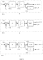
- FIG. 2A is a simplified schematic block diagram of a first exemplary charge pump circuit 100 for a switched capacitor DC-DC converter in accordance with a first embodiment of the invention.
- the switched capacitor DC-DC converter is a step-down topology configured for converting a DC input voltage into a DC output voltage of approximately one-half of the DC input voltage.
- the charge pump circuit 100 comprises a flying capacitor C fly , an output/smoothing capacitor C out and a switch array including a first controllable semiconductor switch SW1, a second controllable semiconductor switch SW2, a third controllable semiconductor switch SW3 and a fourth controllable semiconductor switch SW4.
- Switches SW1 and SW2 are driven by a first clock phase ⁇ 1 of a clock signal and switches SW3 and SW4 are driven by a second clock phase ⁇ 2 of the clock signal as schematically illustrated on the drawing.
- the first and second clock phases ⁇ 1 , ⁇ 2 of the clock signal are complementary and non-overlapping.
- the DC input voltage V in for the charge pump circuit 100 is applied to switch SW1 and the DC output voltage V out is delivered at output/smoothing capacitor C out .
- a load of the charge pump circuit 100 is connected across the output/smoothing capacitor C out and the skilled person will understand the latter supplies energy power to the load when the flying capacitor C fly is charging from the DC input voltage.
- each of the controllable semiconductor switches SW1, SW2, SW3 and SW4 may comprise a MOSFET, e.g. NMOS transistor, or a combination of MOSFETs, as the small size, large off-resistance and low on-resistance of MOSFET switches are advantageous properties in numerous applications of the charge pump circuit 100.
- SW1 is connected between the DC input voltage and a positive terminal of the flying capacitor; SW2 is connected between a negative terminal of the flying capacitor and and the DC output voltage.
- SW2 is connected between the negative terminal of the flying capacitor and a negative DC supply rail, such as GND.
- SW3 is connected between the negative terminal of the flying capacitor and the negative DC supply rail - e.g. GND.
- SW3 is connected between the negative terminal of the flying capacitor and the DC input voltage.
- SW4 is connected between the positive terminal of the flying capacitor and the DC output voltage.
- the first and second switches SW1, SW2 are switched between respective on-states and off-states in accordance with the first clock phase ⁇ 1 and the third and fourth switches SW3, SW4 are switched between respective on-states and off-states in accordance with the second clock phase ⁇ 2 .
- the switch array is configured to, in or during the first clock phase, charge the flying capacitor C fly from the DC input voltage V in through the on-resistances of SW1 and SW2.
- the combined on-resistance of SW1 and SW2 is schematically represented by resistor 2*R SW .
- the switches SW3 and SW4 are off or non-conducting which lead to the equivalent schematic circuit diagram 100a.
- the flying capacitor C fly and output capacitor C out are effectively connected in series between the DC input voltage V in and GND such that the output voltage is charged to approximately one-half of the DC input voltage by periodically switching between the first and second clock phases in steady state operation when no load current is drawn from the output voltage of the charge pump circuit 100.
- the switch array is configured to, in or during the second clock phase ⁇ 2 , discharge the flying capacitor C fly into the output capacitor C out through a charge sharing mechanism due to the parallel connection of the flying capacitor and output capacitor through the conducting states of the switches SW3 and SW4.
- the switches SW1 and SW2 are off, i.e. or non-conducting, which leads to the equivalent schematic circuit diagram 100b.
- the flying capacitor C fly and output capacitor C out are effectively connected in parallel and disconnected from the DC input voltage V in .
- each of the controllable semiconductor switches SW1, SW2, SW3 and SW4 may comprises a control terminal (not shown), e.g. a gate terminal for MOSFETs, to which the first or second clock phases ⁇ 1 , ⁇ 2 are applied to selectively switch the controllable semiconductor switch in question between its on-state and off-state.
- FIG. 2B is a simplified schematic block diagram of a second exemplary charge pump circuit 200 for a switched capacitor DC-DC converter in accordance with a second embodiment of the invention.
- the present embodiment of the switched capacitor DC-DC converter possesses a 3:1 step-down topology configured for converting the DC input voltage V in into a DC output voltage V out of approximately one-third of the DC input voltage.
- the present charge pump circuit 200 comprises, in contrast to the previously discussed pump circuit 100, two separate flying capacitors - a first flying capacitor C fly1 and a second flying capacitor C fly2 .
- the charge pump circuit 200 comprises additionally an output/smoothing capacitor C out and a switch array including a total of seven controllable semiconductor switches controlled by respective clock phases of the first and second non-overlapping clock phases ⁇ 1 , ⁇ 2 as illustrated.
- the switch array is configured to, in or during the first clock phase, simultaneously charge the first flying capacitor C fly1 and second flying capacitor C fly2 from the DC input voltage V in through the on-resistances of active switches. Furthermore, during the first clock phase, the switches operated by the second clock phase ⁇ 2 are off or non-conducting which leads to the equivalent schematic circuit diagram 200a. As illustrated, the first and second flying capacitors and the output capacitor C out are effectively connected in series between the DC input voltage V in and GND, or another negative supply rail, such that the output voltage is charged to approximately one-third of the DC input voltage in steady state operation of the pump circuit for the reasons discussed above in connection with the first charge pump circuit 100.
- the switch array is configured to, during the second clock phase ⁇ 2 , discharge the first and second flying capacitors into the output capacitor C out through a charge sharing mechanism caused by the parallel connection of the first and second flying capacitors and output capacitor through the respective on-resistances of the active/conducting switches.
- the switches operated by the first clock phase ⁇ 1 are off or non-conducting while the switches operated by the second clock phase ⁇ 2 are on or conducting which lead to the equivalent schematic circuit diagram 200b of the charge pump circuit 200.
- the first and second flying capacitors C fly1 and C fly2 and the output capacitor C out are effectively connected in parallel and disconnected from the DC input voltage V in .
- FIG. 3A is a generally applicable model 400 of a switched capacitor DC-DC converter which model is discussed below to highlight some of the properties of the switched capacitor DC-DC converter in accordance with the invention.
- the DC input voltage V in feeds input power or energy to switched capacitor DC-DC converter and during operation the latter generates the DC output voltage V out which may be higher or lower than the DC input voltage depending on the topology of the switched capacitor DC-DC converter as discussed above.
- the switched capacitor DC-DC converter is particularly efficient when the nominal DC input voltage and DC output voltage are related by an certain ratio, illustrated by VCR, such as 1/3 or 1 ⁇ 2 or 2/3 or 2, or 3 or 5 etc.
- the model 400 of the switched capacitor DC-DC converter comprises an ideal transformer 402 with a variable winding ratio as set by the VCR and an equivalent loss resistance R eq connected in series with a secondary winding of the transformer 302.
- the loss resistance R eq comprises two separate resistance components:
- each, or at least a subset, of the controllable semiconductor switches of the switch matrix of the charge pump circuit is formed by a plurality of individually controllable switch segments such that a suitable control device and mechanism may activate merely a subset of the plurality of individually controllable switch segments during activation/turn-on of the corresponding semiconductor switch.
- This use of segmented semiconductor switches provides a controllable on-resistance or equivalently controllable conductance of the semiconductor switch as discussed in additional detail below.
- Graph 350 of FIG. 3B illustrates how the loss resistance R eq of a multi-segmented semiconductor switch comprises two separate resistance components that are individually controllable.
- the y-axis shows the loss resistance R eq on an arbitrary logarithmic scale and the x-axis depicts the clock frequency F S of the clock signal on a logarithmic scale.
- the clock frequency F S is equal to a switching frequency of the flying capacitor as set by the first and second clock phases.
- the loss resistance R eq plots 352, 354, 356, 358 of graph 350 illustrate a particular segmented switch embodiment where each of the controllable semiconductor switches of the switch matrix comprises eight identical individually controllable switch segments connected in parallel. However, other segmented switch embodiments may use fewer or more parallelly connected individually controllable switch segments in each of the controllable semiconductor switches such as between 2 and 16 parallelly connected switch segments.
- the on-resistance, and the equivalent conductance, of a particular controllable semiconductor switch in the present embodiment can be controlled in eight steps by activating from one to eight switch segments via an appropriate set of switch segment control signals applied to the respective controls terminals, e.g. gate terminals, of the switch segments.
- Plot 358 shows schematically by depicting merely asymptotic approximations the loss resistance R eq versus clock frequency F S when all eight switch segments are activated in the on-state or conducting state of the semiconductor switch in question.
- the asymptotic plot 358 comprises two essentially straight portions where the first plot portion 360 shows the loss resistance R eq where the latter is dominated by the first resistance component representing the equivalent output resistance associated with the flying capacitor switching.
- the loss resistance R eq is inversely proportional to the clock frequency F S in the first plot portion 360.
- the second plot portion 364 shows the loss resistance R eq where the latter is dominated by the second resistance component representing the combined on-resistance of the eight parallel switch segments of the semiconductor switch.
- the loss resistance R eq is substantially constant independent of the clock frequency F S in the second plot portion 364 because of the series connection of the first and second resistance components and the diminishing resistance of the first resistance component.
- the knee-point 362 shows the clock frequency F S where the first and second resistance components of loss resistance R eq are essentially equal.
- the plots 356, 354, 352 illustrate schematically the effect of a decreasing number of active switch segments of the semiconductor switch - from eight in plot 358 and down to 4, 2 and 1 active switch segment(s), respectively.
- the loss resistance R eq of the semiconductor switch increases progressively with a decreasing number of active switch segments at higher clock or switching frequencies F S because of the dominating influence of the second resistance component of the loss resistance R eq .
- the loss resistance R eq of the semiconductor switch remains largely independent of the number of active switch segments at very small clock or switching frequencies F S because of the now dominating influence of the first resistance component of the loss resistance R eq .
- FIG. 4 is a simplified schematic block diagram of a switched capacitor (SC) DC-DC converter 400 in accordance with a various exemplary embodiments of the invention.
- the SC DC-DC converter 400 may for example be configured to convert the DC input voltage V in into a DC output voltage V out of approximately one-half of the DC input voltage, i.e. 2:1 step-down, by using merely a single one of the illustrated flying capacitors.
- Other embodiments of the switched capacitor (SC) DC-DC converter 400 may be configured to step-up or boost the input voltage V in into a higher DC output voltage V out for example step-up of 1:2 or 1:3 by appropriate adaption of the topology of the charge pump circuit 100 as discussed above.
- the DC supply voltage to the charge pump circuit 100, and possibly for a gate driver 410, in the latter embodiments may be derived from the higher DC output voltage V out to provide adequately large voltage for the control terminals of the controllable semiconductor switches.
- the DC input voltage V in for the present SC DC-DC converter 400 may be supplied by a rechargeable battery source delivering a nominal DC voltage significantly higher than a desired or optimum voltage for the load circuitry to be energized by the DC output voltage of the SC DC-DC converter 400.
- the rechargeable battery source may for example comprise one or more Li-Ion battery cells that each may exhibit a nominal output voltage of about 3.7 V. If the SC DC-DC converter 100 is integrated in a hearing instrument, it may be desirable to step-down this nominal Li-Ion battery voltage to a DC voltage close to the typical 1.2 V DC level supplied by conventional non-rechargeable Zinc-air hearing aid batteries. Consequently, a DC reference voltage V ref applied at a Ref input of an output voltage regulator or controller 401 may be set to 1.2 V in the latter embodiment of the SC DC-DC converter 400.
- FIG. 1 shows merely four separate first and second complementary and non-overlapping clock phases inputted to the charge pump circuit 100.
- the use of four separate first and second complementary and non-overlapping clock phases is suitable configuration to drive four segmented controllable semiconductor switches SW1, SW2, SW3 and SW4 of the 2:1 step-down SC converter discussed above with reference to FIG. 1 .
- alternative embodiments may comprise additional clock phase signals to drive additional controllable semiconductor switches as indicated previously in connection with the description of the charge pump circuit 200.
- the four, seven or even further controllable semiconductor switches form a switch array which is driven by the first and second non-overlapping clock phases such that the switch array in the first clock phase, charges at least the first flying capacitor C fly1 from the DC input voltage and discharges the first flying capacitor into the output capacitor C out during the second clock phase.
- the charge pump circuit 100 may comprise a so-called "gearbox" combining two or more different converter topologies in combination with a topology switching scheme.
- One such multi-topology embodiment of the charge pump circuit 100 may comprise a 2:1 step-down SC converter and a 3:1 step-down SC converter where the digital switch array controller is configured to select between the 2:1 step-down SC converter and 3:1 step-down SC converter depending on a voltage difference between the DC input voltage V in and the DC output voltage V out .
- This feature may be advantageous to optimize the power conversion efficiency of the charge pump circuit 100 at varying levels of the DC input voltage V in - for example caused by different charging states of the previously discussed rechargeable battery source supplying the DC input voltage to the SC DC-DC converter 400.
- the SC DC-DC converter 400 comprises the output voltage regulator 401.
- the output voltage regulator 401 determines the clock frequency of the charge pump circuit 100 since the first and second non-overlapping clock phases ⁇ 1 , ⁇ 2 are derived from the clock signal sw_clk generated by the output voltage regulator 401 via a digital switch array controller as discussed below.
- the output voltage regulator 401 may comprise a clock generator which is configured for generating the clock signal at a fixed clock frequency or at an adjustable clock frequency.
- the frequency of the clock signal is adjustable or programmable in the present embodiment but alternative embodiments may use a single fixed clock frequency of the clock signal.
- the frequency of the clock signal is utilized to provide regulation of the DC output voltage via a feedback loop extending from the DC output voltage and back to a first input, Sense, of the output voltage regulator 401 via the feedback wire or conductor 425.
- the output voltage regulator 401 additionally comprises a DC reference voltage input, Ref, for receipt of a DC reference voltage V ref indicating the desired or target DC output voltage.
- the feedback loop is operable to minimize a voltage difference or deviation between the DC reference voltage V ref at Ref input and the actual the DC output voltage by adjusting the clock frequency or switching frequency applied to the charge pump circuit 100, via the first and second non-overlapping clock phases ⁇ 1 , ⁇ 2 and/or by adjusting an electrical conductance G SW of the controllable semiconductor switches of the charge pump circuit as discussed in additional detail below.
- the output voltage regulator 401 is configured to select a current clock frequency from a predefined set of fixed clock frequencies while alternative embodiments may adjust the clock frequency in accordance with other frequency control schemes.
- predefined set of fixed clock frequencies allows for frequency planning in the design phase of the output voltage regulator 401 such that the predefined set of fixed clock frequencies may be selected to minimize electromagnetic interference with certain circuits and components of a particular target application such as a hearing instrument as discussed in additional detail below.
- the individual clock frequencies of the predefined set of fixed clock frequencies may be related by integer ratios such as 2, 4, 8 etc., e.g. 500 kHz, 1 MHz, 2 MHz and 4 MHz.
- the digital switch array controller may comprise combinational and sequential digital logic, e.g. implemented as a digital state machine, configured to generate the respective sets of control signals for driving the respective switch segments of the four segmented controllable semiconductor switches SW1, SW2, SW3 and SW4.
- the digital switch array controller comprises a non-overlapping clock generator 403 configured to derive the previously discussed first and second non-overlapping clock phases ⁇ 1 , ⁇ 2 from the clock signal sw_clk supplied by the output voltage regulator 401.
- a first switch encoder 405a of the digital switch array controller utilizes the first clock phase ⁇ 1 and a switch select data supplied via a select bus 404 to generate a first set of switch segment control signals on data bus 407a and likewise utilizes the second clock phase ⁇ 2 and the switch segment select bus 404 to generate a second set of non-overlapping switch segment control signals on data bus 407b.
- the digital switch array controller comprises a gate driver block 410 illustrated as a separate circuit for convenience.
- the gate driver block 410 is configured to generate the required n switch segment control signals 409a for respective ones of the individually controllable switch segments of each of the first and second controllable semiconductor switches SW1, SW2 in accordance with the first clock phase ⁇ 1 and likewise generating the n switch segment control signals 409b for respective ones of the individually controllable switch segments of each of the third and fourth controllable semiconductor switches SW3, SW4 in accordance with the second clock phase ⁇ 2 .
- the gate driver block 410 may for example comprise a plurality of digital buffers, a plurality of level shifters or voltage translators for supplying sufficient drive voltage and current to drive the loads presented by the respective control inputs of the individually controllable switch segments.
- the SC DC-DC converter 400 may include different embodiments of the output voltage regulator 401 providing different switching schemes for unsegmented or segmented versions of the controllable semiconductor switches of the charge pump circuits 100, 200.
- the output voltage regulator 401 a comprises an error signal generator 1001, e.g. a subtraction circuit, configured to subtract the DC reference voltage V ref indicating the desired or target DC output voltage of the SC DC-DC converter 400 and the feedback voltage V out to determine a control signal or error signal ⁇ .
- the error signal ⁇ is applied to the input of a loop filter 1005 which integrates or lowpass filters the error signal to generate a lowpass filtered control signal ⁇ L.
- the lowpass filtered control signal ⁇ L is thereafter applied to the input of a multi-level quantizer 1010, i.e.
- A/D converter configured to convert the lowpass filtered control signal ⁇ L into a corresponding digital control signal at a predetermined sampling frequency.
- the resolution of the multi-level quantizer 1010 may be relatively small for example between 2 bits and 4 bits corresponding to 4 quantization levels and 16 quantization levels, respectively.
- the digital control signal may be representing the current or instantaneous amplitude of the lowpass filtered control signal ⁇ L by between 4 and 16 amplitude levels.
- the predetermined sampling frequency of a multi-level quantizer 1010 may vary between different embodiments of the SC converter and may depend on various design parameters such as the selected clock frequency or clock frequency range and a corner frequency/time constant of a lowpass/integrator response of the loop filter 1005 as discussed in additional detail below.
- the predetermined sampling frequency of the multi-level quantizer 1010 may lie between 500 kHz and 4 MHz. In some embodiments, the predetermined sampling frequency of the multi-level quantizer 1010 may be set at two times the maximum clock or switching frequency F S of the charge pump circuit.
- the charge pump circuit transfers charge to the output capacitor C out on both rising and falling edges of the clock signal which means that voltage ripple on the DC output voltage comprises frequency components located at two times the maximum switching frequency F S .
- the multi-level quantizer e.g. 1010, 1110, 1210, the latter may be sampled synchronously to, or in-phase with, the switching frequency F S to eliminate aliasing products.
- the loop filter 1005 may comprise a so-called PI (proportional-integral) type of filter circuit or filter function comprising a low-frequency gain towards DC, a lowpass pole at a first corner frequency and a zero at a second corner frequency.
- the first corner frequency caused by the lowpass pole is preferably arranged below 100 Hz, or below 50 Hz or below 10 Hz such that a low-frequency response of the loop filter 1005 resembles an integrator response.
- the low-frequency gain may be set to about 70 dB.
- the second corner frequency is preferably significantly higher than the first corner frequency for example at least 20 times higher such as more than 100 times higher.
- the second corner frequency may be located above the audio bandwidth - for example above 20 kHz.
- the gain of the loop filter at low audio frequencies for example below 1 kHz may be set to a relatively large value, e.g. at least 40dB, because loudspeaker drivers, e.g. class D output amplifiers, connected to the DC output voltage tend to draw large currents at low frequencies where the electrical impedance of the loudspeaker typically is small.
- the lowpass characteristics of the loop filters 1005, 1105, 1205 ensures that the SC DC-DC converter 400 often is operating around a single quantization level of the multi-level quantizer 1010, 1110, 1210. Hence, variations of the lowpass filtered control signal ⁇ L between two consecutive sampling points or instances of the multi-level quantizer will not exceed a single quantization level.
- the multi-level quantizer 1010 may be configured to sample markedly less quantization levels at each sampling instant than the number of discrete quantization levels of the multi-level quantizer.
- the present multi-level quantizer may comprise between 8 and 16 quantization levels merely two of these need to be sampled. This will reduce the overall power consumption of the multi-level quantizer 1010 by a factor of four or even eight.
- first corner frequency and the second corner frequency depend on parameter values of other fixed or variable components of the previously discussed feedback loop of the SC DC-DC converter 400 extending from the DC output voltage and back to the sense input of the output voltage regulator 401.
- These other fixed or variable components of the DC-DC converter comprise inter alia the variable loss resistance R eq , the capacitance of the output capacitor C out , the load current, the clock frequency F S of the clock signal sw_clk and a step size of the quantization levels.
- the frequency response of loop filter 1105 including its asymptotic DC gain and asymptotic high-frequency gain, are designed to ensure stability of the feedback loop even at worst parameter values of the above-discussed fixed or variable components of the DC-DC converter.
- the loop filter 1105 may comprise an analog filter or a discrete time filter - for example a fixed switched capacitor PI filter or a programmable switched capacitor PI filter where certain filter characteristics such as the first corner frequency and/or the second corner frequency may be programmable and controlled by the voltage regulator circuit.
- the skilled person will understand that the loop filter 1105 and the error signal generator 1001 may be integrally formed for example as a differential input switched capacitor PI filter.
- the digital signal supplied at the output of multi-level quantizer 1010 may be directly encoded on the previously discussed switch segment select bus 404 (gsw_sel ⁇ 0:7>) such that the binary code on the switch segment select bus 404 directly reflects the amplitude or level of the lowpass filtered control signal ⁇ L.
- This encoding principle is often referred to as "thermometer coding”.
- each of the first, second, third and fourth controllable semiconductor switches SW1, SW2, SW3 and SW4 of the charge pump circuit 100 comprises eight individually controllable switch segments driven by respective sets of switch segment control signals.
- each, or at least one, of the first, second, third and fourth controllable semiconductor switches SW1, SW2, SW3 and SW4 may comprise less than eight individually controllable switch segments or more than eight individually controllable switch segments, e.g. between 2 and 16 individually controllable switch segments to keep a reasonable circuit complexity.
- the on-resistance of the plurality of individually controllable switch segments may be substantially identical or different.
- the plurality of individually controllable switch segments may be coupled in parallel between input and output terminals of each of the controllable semiconductor switches.
- the first and second sets of switch segment control signals applied to the respective switch segments of SW1 and SW2 are derived from the first clock phase by the previously discussed digital switch array controller.
- the third and fourth sets of switch segment control signals applied to the respective switch segments of SW3 and SW4 are derived from the second clock phase by the previously discussed digital switch array controller.
- This arrangement allows the voltage regulator 401 a to provide a variable or adaptive conductance of each of the semiconductor switches SW1, SW2, SW3 and SW4 during converter operation by selecting varying subsets of the eight individually controllable switch segments for each semiconductor switch in accordance with the amplitude of the digital control signal.
- the same subset of switch segments is preferably utilized for each of the semiconductor switches SW1, SW2, SW3 and SW4 for a particular level or amplitude of the digital control signal to simply layout and encoding of the switch control scheme/mechanism of the digital switch array controller.
- the binary value eight on the switch segment select bus 404 may be coded as "11111111" and this value will turn-on all eight individually controllable switch segments of each of the semiconductor switches and provide a maximum conductance, i.e. minimum resistance, of each of the semiconductor switches SW1, SW2, SW3 and SW4 in its on-state.
- Smaller levels of the digital control signal such as two generates a correspondingly smaller binary value on the switch segment select bus 404 e.g. "00000011” due to the thermometer encoding.
- This amplitude level will cause the voltage regulator 401 a to turn-on or activate only two segments of the eight individually controllable switch segments of each of the semiconductor switches leading to a four times smaller conductance of each controllable semiconductor switch compared to the maximum conductance discussed above.
- the present embodiment of the output voltage regulator 401 a may select a switch conductance value, G SW , of each of the first, second, third and fourth controllable semiconductor switches from a set of eight switch conductance values. Consequently, some embodiments of the voltage regulator 401a may be configured to select the respective segment subsets such that the conductance of each of the semiconductor switches SW1, SW2, SW3 and SW4, in its on-state, tracks the amplitude of the digital control signal.
- each of the semiconductor switches SW1, SW2, SW3 and SW4 may be increasing with increasing amplitude of the digital control signal and vice versa since a large amplitude of the digital control signal indicates a large difference between the target or desired DC output voltage V out of the switched capacitor DC-DC converter and the DC reference voltage V ref .
- the electrical conductance of the semiconductor switch or switches can be controlled and exploited by the voltage regulator to control or adjust the DC output voltage V out of the switched capacitor DC-DC converter.
- the output voltage adjustment can be understood by considering the variable loss resistance R eq of the switched capacitor DC-DC converter provided by the adjustable conductance of the semiconductor switches as discussed above.
- R eq of the switched capacitor DC-DC converter provided by the adjustable conductance of the semiconductor switches as discussed above.
- a valuable benefit of segmented semiconductor switches in the charge pump circuit is that only a small fraction, i.e. merely a subset of the plurality of individually controllable switch segments of each of the semiconductor switches need to be activated at small loads. This feature reduces the switching losses incurred by switching on and off the controllable semiconductor switches under such light load conditions and reduces peak currents in the controllable semiconductor switches.
- FIG. 9A illustrates schematically the output voltage regulator 401a which in addition to the previously discussed circuit blocks comprises a clock frequency selector 1015 which selects the frequency of the clock signal sw_clk generated by the output voltage regulator 401 a as discussed above.
- the output voltage regulator preferably comprises an adjustable clock generator (not shown) configured to generate a predefined set of fixed clock frequencies such as between more than two, three or four fixed clock frequencies for example between two and eight fixed clock frequencies.
- the output voltage regulator is configured to switch between these individual clock frequencies of the predefined set of fixed clock frequencies in accordance with the level or amplitude of the digital control signal to provide an additional, or even alternative, control mechanism for adjusting the DC output voltage V out of the switched capacitor DC-DC converter.
- This output voltage adjustment mechanism can be understood by considering the variance of the first resistance component, of the loss resistance R eq of the switched capacitor DC-DC converter, representing the equivalent output resistance associated with the switching of the one or more flying capacitors.
- the provision of the predefined set of fixed clock frequencies enable system level frequency planning where the present switched capacitor DC-DC converter only generates noise disturbances at frequencies where the remaining portion of the system is insensitive to noise or at least has reduced sensitivity to noise.
- the reference to system level means the complete portable communication device, such as a hearing instrument, in which the present switched capacitor DC-DC converter is to be exploited for DC power supply purposes as discussed in additional detail below.
- the individual clock frequencies of the predefined set of fixed clock frequencies are preferably related by an integer factor for example 2, 3, 4 or 8. In this manner, the ripple noise components on the DC output voltage and emitted electromagnetic noise components are located at known and well-defined regions of the frequency spectrum despite the switching between these individual clock frequencies.
- FIG. 5 shows on graph 500 an exemplary waveform 502 of the lowpass filtered control signal ⁇ L "Control signal" generated by the output voltage regulator 401 a illustrated on FIG. 9A ).
- the output voltage regulator 401 a comprises an eight-level quantizer or A/D converter.
- Each of the semiconductor switches, e.g. SW1, SW2, SW3 and SW4, of the charge pump circuit comprises eight individually controllable switch segments.
- the output voltage regulator 401 a comprises an adjustable/programmable clock generator (not shown) configured to generate a predefined set of fixed clock frequencies consisting at least of clock frequencies 250 kHz, 500 kHz and 1 MHz.
- the eight quantization levels of the eight-level quantizer are illustrated by horizontal dotted lines on graph 500 and the corresponding selection of the subset of individually controllable switch segments are indicated at column 505 where Gsw6 correspond to six active switch segments and Gsw2 correspond to two active switch segments etc.
- Graph 520 also illustrates the dynamic or adaptive subset selection of individually controllable switch segments carried out by the output voltage regulator 401 a in dependence of the varying level of the lowpass filtered control signal ⁇ L where the y-axis shows how the number of active switch segments varies over time.
- Graph 510 illustrates the dynamic or adaptive selection of the clock frequency carried out by the output voltage regulator 401 a in dependence of the varying level of the lowpass filtered control signal ⁇ L.
- the instantaneous clock frequency selection is also indicated in column 507 illustrating how the clock frequency selection is coupled to a particular set or sets of active switch segments, i.e. five or six active switch segments Gsw5, Gw4 is coupled to the highest 1 MHz clock frequency and so on.
- the adjustable clock frequency/switching frequency of the output voltage regulator 401 a provides a flexible adaptation mechanism of the DC-DC converter to changing load conditions such that a high switching frequency may be selected under heavy load conditions and a low switching frequency under light load conditions for the benefit of minimizing switching losses in the first, second, third and fourth controllable semiconductor switches SW1, SW2, SW3 and SW4 as well as other switched components of the DC-DC converter.
- FIG. 9B shows a simplified block diagram of a second embodiment of the output voltage regulator 401 b.
- the output voltage regulator 401 b comprises a number of corresponding circuit blocks to those discussed above such as an error signal generator, e.g. a subtraction circuit 1101, configured to subtract the DC reference voltage V ref indicating the target DC output voltage of the SC DC-DC converter 400 and the feedback voltage V out to determine a control signal or error signal ⁇ .
- the output voltage regulator 401 b also comprises a loop filter 1105, a multi-level quantizer 1110, i.e. A/D converter, configured to convert the lowpass filtered control signal ⁇ L into a corresponding digital control signal at a predetermined sampling frequency as discussed above.
- the output voltage regulator 401 b comprises a digital switch array controller 1120 that implements a toggle triggered control scheme to the controllable semiconductor switches, e.g. SW1, SW2, SW3 and SW4, of the charge pump circuit via the switch segment select bus 404 (gsw_sel ⁇ 0:7>) and the clock signal sw_clk.
- the digital switch array controller 1120 is configured to toggle only the clock signal sw_clk to the charge pump circuit when it is necessary.
- the digital switch array controller 1120 is configured to use a minimum switch conductance of each of the controllable semiconductor switches for a current clock or switching frequency. This control mechanism provides a non-repetitive waveform of the clock signal sw_clk 625 generated by the output voltage regulator 401 b such that the frequency spectrum of the clock signal varies with time and is difficult to estimate or control.
- Graph 600 shows an exemplary waveform 602 of the lowpass filtered control signal ⁇ L "Control output" generated by the output voltage regulator 401 b illustrated on FIG. 9B ).
- the output voltage regulator 401 b comprises an eight-level quantizer or A/D converter.
- Each of the semiconductor switches, e.g. SW1, SW2, SW3 and SW4, of the charge pump circuit comprises eight individually controllable switch segments.
- the eight quantization levels of the eight-level quantizer are illustrated by horizontal dotted lines on graph 600 and the corresponding selection of the subset of individually controllable switch segments are indicated graphs 610, 620 and 630 where the number of active switch segments, and thereby increasing switch conductance, are indicated on the y-axis.
- the x-axis shows time to illustrate how the number of active switch segments changes over time.
- Graphs 610, 620 and 630 shows different operating conditions of the output voltage regulator 401 b designated "normal”, “soft chop” and “hard chop.
- the digital switch array controller In the "normal” mode, the digital switch array controller only acts when the lowpass filtered control signal ⁇ L "Control signal" waveform 602 crosses a quantization level in upwards direction.
- the clock is toggled and the switch conductance associated with the just passed quantization level is turned on. No conductance switching is on the other hand carried when the lowpass filtered control signal again falls below a quantization level which leads to a low power consumption as the switch segments only switches very rarely.
- the digital switch array controller will respond by reducing the charge transfer to the charge pump circuit using this extra information of the falling crossing of a quantization level.
- the switch controller switches off the switch segment with highest conductance of ones currently on, or just anyone of the switch segments if they have identical conductance, to reduce the charge transfer.
- the controller turns off all the switch segments. However, in general any number of the individual switch segments could be turned off in response to a downward crossing of a quantization level.
- FIG. 9C shows a simplified block diagram of a third embodiment of the output voltage regulator 401 c.
- the output voltage regulator 401 c comprises a number of corresponding circuit blocks to those discussed above such as an error signal generator, e.g. a subtraction circuit 1201, configured to subtract the DC reference voltage V ref indicating the desired or target DC output voltage of the SC DC-DC converter 400 and the feedback voltage Vout to determine a control signal or error signal ⁇ .
- the output voltage regulator 401 also comprises a loop filter 1205, a multi-level quantizer 1210, i.e. A/D converter, configured to convert the lowpass filtered control signal ⁇ L into a corresponding digital control signal at a predetermined sampling frequency as discussed above.
- a multi-level quantizer 1210 i.e. A/D converter
- the output voltage regulator 401 c comprises a digital switch array controller or adder 1230 that implements a binary weighted control scheme.
- the digital switch array controller 1230 can select the eight, or any other practical integer number, individually controllable switch segments weighted as binary numbers to provide 2N possible switch conductance values where N is the number of individual switch segments of each of the controllable semiconductor switches of the charge pump circuit.
- This control mechanism or scheme provides a significantly better conductance resolution for the controllable semiconductor switches, e.g. SW1, SW2, SW3 and SW4, and may eliminate certain shortcomings caused by a more limited conductance resolution of the above discussed first and second embodiments of the output voltage regulator 401 a, 401 b using merely eight possible conductance values.
- the digital switch array controller or adder 1230 is clocked at a fixed or variable adder clock frequency.
- the clock frequency can be adjusted between a fixed set of individual clock frequencies comprising 2 MHz, 1 MHz, and 500 kHz.
- the switch conductance value, Gsw, of each of the controllable semiconductor switches may be updated on both rising and falling edge of the clock signal. This provides minimal voltage ripple on the DC output voltage and an accurate output voltage regulation.
- a reduction of the clock frequency to e.g. 1 MHz or 500 kHz will lead to larger ripple voltage but with the benefit of reduced power dissipation in the multi-level quantizer.
- FIG. 7 shows on graph 700 an exemplary waveform 702 of the lowpass filtered control signal ⁇ L "Control signal" generated by the output voltage regulator 401 c illustrated on FIG. 9C ) comprising an exemplary eight-level quantizer.
- Each of the semiconductor switches SW1, SW2, SW3 and SW4 of the charge pump circuit comprises eight binary weighted individually controllable switch segments leading to 255 individually selectable switch conductance values, G SW , of each of the first, second, third and fourth controllable semiconductor switches.
- the output voltage regulator 401 c may also comprise a clock frequency selector 1215 which selects the frequency of the clock signal sw_clk generated at the output voltage regulator 401 a.
- the clock frequency selector 1215 is configured to generate a predefined set of fixed clock frequencies e.g. consisting at least of clock frequencies 250 kHz, 500 kHz and 1 MHz.
- a subset of the quantization levels of the multi-level quantizer are illustrated by horizontal dotted lines on graph 700 and the amplitude of the digital control signal determines the conductance value that is added to or subtracted from a current conductance value of the each of the controllable semiconductor switches by the adder 1230.
- the illustrated embodiment uses the conductance values +1/+2/+4 and -1/-2/-4 as indicated by column 705, but this election of conductance levels may be different in other embodiments.
- the output voltage regulator 401 c is configured to select a current clock frequency F S of the clock signal sw_clk based on a current switch conductance of each of the first, second, third and fourth controllable semiconductor switches SW1, SW2, SW3 and SW4 using a relatively simple mapping rule such as:
- the digital switch array controller may be adapted to implement a simple mapping rule to ensure that the output voltage regulator 401 c increases both the clock frequency and the switch conductance for increasing amplitude of the digital control signal and vice versa.
- a certain value (e.g. +/- 1, 2, 4) may for example be added in each adder clock period.
- Gsw When a certain threshold for the switch conductance value Gsw is reached, the switch controller switches to a higher or lower clock frequency. If the switch conductance value is held constant and the clock frequency Fsw is suddenly doubled a very large reduction of output resistance of the converter is introduced within a single adder period. This is typically an undesirable effect and the switch array controller may therefore be configured to switch reduce the current value of the switch conductance in response to switching to a higher clocking frequency.
- a corresponding scheme may be implemented by the switch array controller when jumping to a lower clock frequency. For example if the switch conductance value is constant and the clock frequency is halved, a large increase of the output resistance results. This increase of output resistance may be compensated by increasing the switch conductance value by an appropriate amount in response to the clock frequency reduction.
- FIG. 9 illustrates the operation of a fourth embodiment of the output voltage regulator 401 via graphs 910, 920 and 930.
- the output voltage regulator 401 comprises a digital switch array with a segmented structure of the controllable semiconductor switches of the charge pump circuit 100, 200 similar to anyone of the previously discussed first, second and third embodiments of the output voltage regulator 401.
- Each of the controllable semiconductor switches of the charge pump circuit may comprise between 2 and 16 individually controllable switch segments driven by respective sets of switch segment control signals as discussed above.
- Graph 910 illustrates the ordinary waveforms of the first and second clock phases ⁇ 1 , ⁇ 2 of the clock signal driving at least one of, and preferably all of, the controllable semiconductor switches of the charge pump circuit.
- Graph 920 illustrates waveforms of the first and second clock phases ⁇ 1 , ⁇ 2 of the clock signal driving at least one of, and preferably all of, the controllable semiconductor switches of the charge pump circuit in accordance with the fourth embodiment of the output voltage regulator.
- Each of the controllable semiconductor switches is turned-on and turned-off in a gradual or stepped manner by sequentially turn-on and turn-off the plurality, e.g. eight, of the individually controllable switch segments.
- the plurality of individually controllable switch segments of a particular controllable semiconductor switch may be switched between on and off states by a corresponding set of switch segment control signals.
- the switch conductance G SW changes gradually from zero to 4 in a step-wise fashion where each step indicates the activation of an additional switch segment of the controllable semiconductor switch in question.
- each of the controllable semiconductor switches is turned-on gradually or stepwise, e.g. in four discrete steps, as illustrated, by introducing a suitable time delay between the switch segment control signals.
- the switch conductance G SW changes gradually from four and down-to zero in a correspondingly step-wise manner where each step indicates the deactivation or switch off of an additional switch segment.
- the time delay between two adjacent switch segment control signals will vary depending on various design factors such the number of individually controllable switch segments.
- the time delay between two adjacent switch segment control signals may correspond to about 0.04-0.4 % of the period time t p of the first or second clock phase such that the total turn on time and turn off time of a controllable switch mat lie between 0.28-2.8 % of the period time t p for an eight segment switch.
- the period time t p of the first or second clock phase may lie between 0.5 ⁇ s and 4 ⁇ s corresponding to a clock or switching frequency of the voltage pump circuit between 125 kHz and 2 MHz.
- Graph 930 illustrates schematically current waveforms l Cfly of the current flowing into and out of the flying capacitor or capacitors of the charge pump circuit where a first waveform 935 shows the flying capacitor current for the switch segment selection scheme on graph 910.
- the second (dotted line) current waveform 940 shows the flying capacitor current using the sequential turn-on scheme for switch segments illustrated on graph 920 where the switch conductance G SW changes gradually over time in accordance with the fourth embodiment of the output voltage regulator.
- the second flying capacitor current waveform 940 has markedly reduced rate of change, dl/dt, compared to the first flying capacitor current waveform 935.
Abstract
Description
- The present invention relates to a hearing instrument comprising a rechargeable battery source providing a battery supply voltage and a switched capacitor DC-DC converter comprising a DC input coupled to the battery supply voltage for converting the battery supply voltage into a higher or lower DC output voltage. The hearing instrument comprises at least one active circuit connected to the DC output voltage for energizing active components of the at least one active circuit.
- Switched capacitor DC-DC power converters are known in the art and have previously been applied in various types of portable communication devices. Switched capacitor DC-DC power converters are utilized to convert a DC input voltage from an energy or power source, such as a rechargeable battery, of the portable device into a higher or lower DC output voltage suitable for powering various types of integrated circuits and other active components. Switched capacitor DC-DC power converters possess certain attractive properties compared to their inductor-based counterparts - for example a relatively low level of EMI, because there is not stored energy in magnetic fields of inductors. Switched capacitor DC-DC power converters may have small size and high energy conversion efficiency. Different topologies of switched capacitor DC-DC power converters are capable of providing DC voltage step-up (i.e. boost) and DC voltage step-down (i.e. buck) with a topology dependent optimum voltage conversion ratio for example 1:2 or 1:3 step-up conversion and 2:1 and 3:1 step-down conversion.
- However, there remains a need in the art to provide switched capacitor DC-DC power converters with improved performance characteristics such as higher power conversion efficiency across a wide range of loads, even further reduction of electromagnetic noise emission, reduced voltage ripple on the DC output voltage, improved source regulation and improved load regulation etc. Switched capacitor DC-DC converters are highly useful for powering hearing instruments where the compact dimensions of the housing or custom shell in conjunction with small battery capacity typically place severe constraints on size, power conversion efficiency and electromagnetic emissions of the power supply circuitry. Furthermore, magnetic field emissions generated by magnetics/inductor based DC-DC power converters are prone to disturb RF signal receipt and transmission of RF wireless transceivers present in the hearing instrument.
- A first aspect of the invention relates to a hearing instrument comprising:
- a rechargeable battery source providing a battery supply voltage. The hearing instrument comprises a switched capacitor DC-DC converter comprising a DC input coupled to the battery supply voltage for converting the battery supply voltage into a higher or lower DC output voltage. At least one active circuit of the hearing instrument is connected to the DC output voltage for energizing active components of the at least one active circuit.
- The hearing instrument may comprise a housing or shell according to any known housing style such as Behind-the-Ear (BTE), In-the-Ear (ITE), In-the-Canal (ITC), Completely-in-Canal (CIC) etc. The hearing instrument may comprise one or several microphone(s) for picking-up sound from the external environment of the hearing instrument and generate a first audio signal in response.
- The least one active circuit may comprise a plurality of active circuits, or circuit blocks, configured to carry out respective processing functions of the hearing instrument such as amplifying, compressing, filtering, beamforming one or more audio signals, e.g. speech or music, picked-up by the microphone or microphone of the hearing instrument. The least one active circuit may comprise a plurality of interconnected transistors forming a digital logic circuit or an analog circuit or a combination of both. The least one active circuit may comprise a class D output amplifier as discussed in further detail below.
- The rechargeable battery source may comprise at least one Li-Ion battery cell delivering the battery supply voltage to the DC input of the switched capacitor DC-DC converter. Since, Li-Ion battery cells supply a nominal battery voltage at around 4.0 V, the switched capacitor DC-DC converter may be configured to step-down the batter supply voltage with a factor of 2:1 and/or 3:1, depending on a charging state of the at least one Li-Ion battery cell, to supply a DC output voltage of about 1.2 V to the least one active circuit of the hearing instrument. The latter voltage at around 1.2 V is often optimal or near-optimal for the class D output amplifier and other active circuits of the hearing instrument as discussed below. However, the skilled person will understand the switched capacitor DC-DC converter may be configured to step-up the batter supply voltage with certain ratios, e.g. 1:2 and/or 1:3, for other types of rechargeable battery sources delivering nominal battery voltages below 1.2 V.
- The least one active circuit of the hearing instrument may comprise a control and processing circuit which comprises:
- a first audio input channel for receipt of the first audio signal,
- a signal processor for receipt and processing of the audio signal for generating a compensated microphone signal according to a hearing loss of a user;
- wherein the compensated microphone signal is applied to an audio input of the class D output amplifier for generation of a modulated output signal at a predetermined modulation frequency for application to a miniature receiver or loudspeaker.
- The signal processor of the hearing instrument may comprise dedicated digital logic circuitry, a software programmable processor or any combination thereof. As used herein, the terms "processor", "signal processor", "controller", "system", etc., are intended to refer to microprocessor or CPU-related entities, either hardware, a combination of hardware and software, software, or software in execution. For example, a "processor", "signal processor", "controller", "system", etc., may be, but is not limited to being, a process running on a processor, a processor, an object, an executable file, a thread of execution, and/or a program. By way of illustration, the terms "processor", "signal processor", "controller", "system", etc., designate both an application running on a processor and a hardware processor. One or more "processors", "signal processors", "controllers", "systems" and the like, or any combination hereof, may reside within a process and/or thread of execution, and one or more "processors", "signal processors", "controllers", "systems", etc., or any combination hereof, may be localized on one hardware processor, possibly in combination with other hardware circuitry, and/or distributed between two or more hardware processors, possibly in combination with other hardware circuitry. Also, a processor (or similar terms) may be any component or any combination of components that is capable of performing signal processing. For examples, the signal processor may be an ASIC processor, a FPGA processor, a general purpose processor, a microprocessor, a circuit component, or an integrated circuit.
- The hearing instrument may comprise a wireless receiver coupled to the first audio input channel for receipt of a wireless modulated audio signal and a decoder coupled to the wireless receiver for extracting a wireless audio signal and coupling the wireless audio signal to the first audio input channel or a second audio input The wireless receiver may comprise an appropriate antenna for the selected type of wireless transmission such as an RF antenna or a magnetic antenna. The RF antenna may for example be configured for receipt of a wireless modulated audio signal according to the Bluetooth standard or the Bluetooth Low energy (Bluetooth LE) standard. Alternatively, a much lower frequency of communication may be applied for example based on magnetic coupling in which case the magnetic antenna may comprise a traditional telecoil.
- The hearing instrument may additionally comprise an output transducer, such as a receiver, loudspeaker, implanted electrode transducer etc., configured to supply the modulated output signal based on the hearing loss compensated microphone signal. The auditory output signal is perceived by the hearing instrument user's auditory system as sound.
- A preferred embodiment of the switched capacitor DC-DC converter comprises:
- a clock generator configured to generate a clock signal,
- a charge pump circuit comprising a switch array driven by first and second non-overlapping clock phases derived from the clock signal; said switch array configured to, in a first clock phase, charge a flying capacitor from the DC input voltage and, in a second clock phase, discharge the flying capacitor into an output capacitor connected to the DC output voltage. The switched capacitor DC-DC converter additionally comprises an output voltage regulator which comprises:
- a reference voltage input for receipt of a DC reference voltage and a feedback voltage input for receipt of a feedback voltage representative of the DC output voltage,
- an error signal generator configured to combine the DC reference voltage and the feedback voltage to determine a control signal,
- a loop filter configured for receipt and lowpass filtering of the control signal to generate a lowpass filtered control signal,
- a multi-level quantizer configured to convert the lowpass filtered control signal into a corresponding digital control signal at a predetermined sampling frequency,
- a switch array controller configured to generate the first and second non-overlapping clock phases for the charge pump circuit based on the clock signal and digital control signal.
- The sampling frequency of the multi-level quantizer may lie above 500 kHz for example between 1 MHz and 8 MHz. According to one embodiment of the switched capacitor DC-DC converter, the predetermined sampling frequency of the multi-level quantizer equals to two times a maximum clock frequency of the clock signal which drives the charge pump circuit via the first and second non-overlapping clock phases. The charge pump circuit may transfer charge to the DC output voltage, and to a smoothing or output capacitor connected thereto, on both rising and falling edges of the clock signal. This means that voltage ripple on the DC output voltage comprises frequency components located at two times the maximum clock frequency of the clock signal and harmonics thereof. In certain advantageous embodiments of the invention, the multi-level quantizer may be sampled synchronously to the clock signal to suppress aliasing products associated with the sampling of the lowpass filtered control signal.
- The multi-level quantizer, aka A/D converter, may comprise between 2 and 16 quantization levels depending on the requirements of a particular application for accuracy, circuit complexity and power consumption.
- The switch array may comprise a plurality of controllable semiconductor switches selectively connecting one or more flying capacitors to the DC input voltage and charging the one or more flying capacitor(s) and alternatingly discharging the one or more flying capacitor(s) into the output capacitor at the DC output voltage. Certain embodiments of the switch array may comprise at least one flying capacitor and a first controllable semiconductor switch connected between the DC input voltage and a positive terminal of the flying capacitor;
a second controllable semiconductor switch connected between a negative terminal of the flying capacitor and one of a negative DC supply rail, such as ground, and the DC output voltage;
a third controllable semiconductor switch connected between a negative terminal of the flying capacitor and the negative DC supply rail;
a fourth controllable semiconductor switch connected between the positive terminal of the flying capacitor and the DC output voltage; wherein
the first and second controllable semiconductor switches are switched between respective on-states and off-states in accordance with the first clock phase and the third and fourth controllable semiconductor switches are switched between respective on-states and off-states in accordance with the second clock phase. - The loop filter may comprise an analog lowpass filter and/or a discrete time lowpass filter such as a switched capacitor lowpass filter. The skilled person will understand that the loop filter and the error signal generator may be integrally formed for example as a differential input switched capacitor filter configured to subtracting the DC reference voltage and the feedback voltage and to lowpass filtering the control signal as discussed in additional detail below with reference to the appended drawings.
- The loop filter preferably comprises a so-called proportional integral filter such that a transfer function of the loop filter comprises a lowpass pole at a first corner frequency of the transfer function. The first corner frequency may be smaller than 200 Hz, such as smaller than 100 Hz, or smaller than 10 Hz, to approximate the functionality of a true integrator. The transfer function of the loop filter may in certain embodiments also comprise and a zero at a second corner frequency. The second corner frequency is preferably significantly higher than the first corner frequency for example at least 20 times higher such as more than 100 times higher. The second corner frequency may be located above the audio bandwidth - for example above 20 kHz. The transfer function of one embodiment of the loop filter has the first corner frequency located at 50 Hz and the second corner frequency located at 26 kHz.
- A number of useful embodiments of the switched capacitor DC-DC converter comprise a plurality of controllable semiconductor switches which possess adjustable on-resistance or conductance. One such embodiment of the switched capacitor DC-DC converter comprises first and second controllable semiconductor switches which each comprises a plurality of individually controllable switch segments driven by first and second sets of switch segment control signals, respectively, derived from the first clock phase; and each of the third and fourth controllable semiconductor switches comprises a plurality of individually controllable switch segments driven by third and fourth sets of switch segment control signals, respectively, derived from the second clock phase. One or more of the controllable semiconductor switches of the switch array may each comprise between 2 and 16 individually controllable switch segments. The respective resistances of the plurality of individually controllable switch segments may be substantially identical or they may differ - for example following a binary weighted scheme.
- The output voltage regulator may be configured to, for one or more of the first, second, third and fourth controllable semiconductor switches, selecting respective segment subsets of the plurality of individually controllable switch segments in accordance with an amplitude of the digital control signal. The output voltage regulator may for example be configured to selecting the respective switch segment subsets such that a conductance of each of the one or more of the first, second third and fourth controllable semiconductor switches, in its on-state, tracks the amplitude of the digital control signal for example increasing the number of active switch segments, i.e. conducting switch segments, of the plurality of individually controllable switch segments with increasing amplitude of the digital control signal, and possibly vice versa , to increase charge transfer to the DC output voltage and counteract the increase of the amplitude of the digital control signal. The increasing amplitude of the digital control signal indicates an increasing output voltage error at the DC output voltage and vice versa for decreasing amplitude of the digital control signal. The skilled person will understand that a segment subset at some time instances may comprise all of the individually controllable switch segments to maximize the conductance of the controllable semiconductor switch in question.
- One attractive variant of the switched capacitor DC-DC converter comprises a plurality of controllable semiconductor switches that are switched on and switched off in a gradual or stepwise manner by sequentially activating the switch segments in connection with a state switching of the controllable semiconductor switch. According to one such embodiment, the output voltage regulator is configured to:
- switch between on-states and off-states of the first controllable semiconductor switch by sequentially turn-on and turn-off the plurality of individually controllable switch segments via the first set of switch segment control signals; and/or
- switch between on-states and off-states of the second controllable semiconductor switch by sequentially turn-on and turn-off the plurality of individually controllable switch segments via the second set of switch segment control signals; and/or
- switch between on-states and off-states of the third controllable semiconductor switch by sequentially turn-on and turn-off the plurality of individually controllable switch segments via the third set of switch segment control signals; and/or
- switch between on-states and off-states of the fourth controllable semiconductor switch by sequentially turn-on and turn-off the plurality of individually controllable switch segments via the fourth set of switch segment control signals.
- The output voltage regulator may be configured to, for the one or more of the first, second third and fourth controllable semiconductor switches:
- toggling the first and second clock phases in response to the amplitude of the digital control signal is incremented from a current quantization level to a larger quantization level; and
- selecting respective segment subsets of the plurality of individually controllable switch segments in accordance with the amplitude of the digital control signal.
- According to yet another embodiment of the switched capacitor DC-DC converter, the clock generator is configured to generate a predefined set of individually selectable fixed clock frequencies such as at least two fixed clock frequencies for example between two and eight fixed clock frequencies. According to this embodiment, the individually selectable fixed clock frequencies may be generated by a programmable or adjustable clock generator and the latter controlled by the output voltage regulator. The output voltage regulator may be configured to switch between these individual clock frequencies of the predefined set of fixed clock frequencies in accordance with the level or amplitude of the digital control signal to provide a control mechanism for adjusting the DC output voltage of the switched capacitor DC-DC converter. The output voltage regulator may for example increase the clock frequency for increasing amplitude of the digital control signal and decrease the clock frequency for decreasing amplitude of the digital control signal as discussed in additional detail below with reference to the appended drawings.
- The provision of this predefined set of fixed clock enables system level frequency planning where the switched capacitor DC-DC converter only generates ripple voltage disturbances at frequencies where the remaining portion of the system, e.g. the at least one active circuit block, is insensitive to noise, or at least exhibits, a reduced sensitivity to noise for example residing on the DC output voltage or picked-up as electromagnetic waves, i.e. EMI disturbances. The output voltage regulator may be configured to select a clock frequency from the predefined set of fixed clock frequencies in accordance with a predetermined modulation frequency of the previously mentioned class D output amplifier coupled to the DC output voltage of the switched capacitor DC-DC converter for power supply. This is beneficial because class D output amplifiers typically possess relatively poor power supply rejection ratio (PSRR) due to a noise shaping mechanism pushing a high level of quantization noise above the audio band in the noise-shaped output signal as discussed in additional detail below with reference to the appended drawings. According to one such embodiment of the output voltage regulator, each clock frequency of the predefined set of fixed clock frequencies is an integer multiple of the predetermined modulation frequency of the class D output amplifier. The modulation frequency of class D output amplifier may for example be set to 250 kHz and the predefined set of fixed clock frequencies of the output voltage regulator comprising at least 250 kHz, 500 kHz and 1 MHz or at least 500 kHz, 1 MHz and 1.5 MHz. The skilled person will understand that the clock signal of the switched capacitor DC-DC converter preferably is synchronous to a clock signal setting the predetermined modulation frequency of the class D output amplifier to maintain a well-defined relationship between the switching frequencies of the switched capacitor DC-DC converter and the modulation frequency of class D output amplifier despite temperature variations and component drift etc.
- The individual clock frequencies of the predefined set of fixed clock frequencies may be related by integer ratios such as 2, 3, 4, 8 etc. The predefined set of fixed clock frequencies may e.g. comprise 500 kHz and 1 MHz or comprise 250 kHz, 500 kHz, 1 MHz and optionally 2 MHz.
- The output voltage regulator may adhere to a predetermined table or predetermined rule specifying a coupling between the amplitude of the digital control signal, the predefined set of fixed clock frequencies and the active switch segment subset of each of the controllable semiconductor switches. In one such embodiment the output voltage regulator comprises a predetermined table or predetermined rule mapping each amplitude of the digital control signal to a particular combination of clock frequency, selected from predefined set of individually selectable fixed clock frequencies, and switch segment subsets of the plurality of individually controllable switch segments. The skilled person will understand that this predetermined table or predetermined rule may be implemented by a suitably configured digital state machine of the switch array controller.
- A second aspect of the invention relates to a switched capacitor DC-DC converter configured for converting a DC input voltage into a higher or lower DC output voltage. The switched capacitor DC-DC converter comprising:
- a clock generator configured to generate a clock signal,
- a charge pump circuit comprising a switch array driven by first and second non-overlapping clock phases derived from the clock signal; said switch array configured to, in a first clock phase, charge a flying capacitor from the DC input voltage and, in a second clock phase, discharge the flying capacitor into an output capacitor connected to the DC output voltage. The switched capacitor DC-DC converter further comprises an output voltage regulator which comprises:
- a reference voltage input for receipt of a DC reference voltage and a feedback voltage input for receipt of a feedback voltage representative of the DC output voltage,
- an error signal generator configured to combine the DC reference voltage and the feedback voltage to determine a control signal,
- a loop filter configured for receipt and lowpass filtering of the control signal to generate a lowpass filtered control signal,
- a multi-level quantizer configured to convert the lowpass filtered control signal into a corresponding digital control signal at a predetermined sampling frequency,
- a switch array controller configured to generate the first and second non-overlapping clock phases for the charge pump circuit based on the clock signal and digital control signal.
- Embodiments of the invention will be described in more detail in connection with the appended drawings, in which:
-
FIG. 1 shows a simplified schematic block diagram of hearing instrument comprising an exemplary switched capacitor DC-DC converter according to any of the below-described embodiments thereof; -
FIG. 2A ) is a simplified schematic block diagram of a first exemplary charge pump circuit for a switched capacitor DC-DC converter in accordance with a first embodiment of the invention, -
FIG. 2B ) is a simplified schematic block diagram of a second exemplary charge pump circuit for a switched capacitor DC-DC converter in accordance with a second embodiment of the invention, -
FIG. 3A ) shows a generally applicable electrical model of a switched capacitor DC-DC converter, -
FIG. 3B ) shows a model of the loss resistance Req of a second exemplary charge pump circuit comprising a plurality of multi-segmented semiconductor switches, -
FIG. 4 is a simplified schematic block diagram of an exemplary switched capacitor (SC) DC-DC converter in accordance with a various embodiments of the invention, -
FIG. 5 shows a waveform of a lowpass filtered control signal generated by a first output voltage regulator embodiment of the exemplary SC DC-DC converter, -
FIG. 6 shows a waveform of a lowpass filtered control signal generated by a second output voltage regulator embodiment of the exemplary switched capacitor SC DC-DC converter, -
FIG. 7 shows a waveform of a lowpass filtered control signal generated by a third output voltage regulator embodiment of the exemplary switched capacitor (SC) DC-DC converter, -
FIG. 8 illustrates the operation of a fourth embodiment of the output voltage regulator comprising a segmented switch structure with sequential turn-on and turn-off of the individually controllable switch segments, -
FIG. 9A ) shows a simplified block diagram of the first output voltage regulator embodiment of the exemplary SC DC-DC converter, -
FIG. 9B ) shows a simplified block diagram of the second output voltage regulator embodiment of the exemplary SC DC-DC converter; and -
FIG. 9C ) shows a simplified block diagram of the third output voltage regulator embodiment of the exemplary SC DC-DC converter. - In the following, various exemplary embodiments of the present hearing instrument, comprising a switched capacitor DC-DC converter for energy efficient DC voltage conversion, are described with reference to the appended drawings. The skilled person will understand that the appended drawings are schematic and simplified for clarity and therefore merely show details which are essential to the understanding of the invention, while other details have been left out. Like reference numerals refer to like elements or components throughout. Like elements or components will therefore not necessarily be described in detail with respect to each figure. The skilled person will further appreciate that certain actions and/or steps may be described or depicted in a particular order of occurrence while those skilled in the art will understand that such specificity with respect to sequence is not actually required.
-
FIG. 1 shows a simplified schematic block diagram of anexemplary hearing instrument 1300 comprising a switched capacitor DC-DC converter according to any of the below-described embodiments thereof. The DC input voltage input of the switched capacitor DC-DC converter 400 is connected to a rechargeable battery source VDD. The rechargeable battery source is connected to thehearing instrument circuitry 1300, including an integrally formed switched capacitor DC-DC converter 1350, through a positivepower supply terminal 1309. The skilled person will understand that the battery source in other embodiments of the invention may comprise a non-rechargeable battery source where it is desired to step-up or step-down the nominal DC voltage level supplied by such non-rechargeable battery source to a different DC voltage level more optimal, e.g. lower power consumption, for active circuits or circuit blocks. Thehearing instrument 1300 may comprise any type of hearing aid housing style such as Behind-the-Ear (BTE), In-the-Canal (ITC), Completely-in-Canal (CIC), RIC etc. - The rechargeable battery source may comprise at least one Li-Ion battery cell and may hence supply a nominal DC input voltage VDD at around 4.0 V to the switched capacitor DC-
DC converter 400. The switched capacitor DC-DC converter 400 is configured to step-down the received DC input voltage with a factor of approximately 2:1 and/or 3:1 to supply a DC output voltage Vout of about 1.2 V. An output/smoothing capacitor Cout is connected to the DC output voltage Vout and at least one flying capacitor Cfly is connected to a switch array of the converter as previously discussed. The 1.2 V DC output voltage typically provides optimum or near-optimum power supply conditions for the individual active circuits or circuit blocks of the hearing instrument, in particular for a classD output amplifier 1313, such that the battery life of the hearing instrument is maximized. The optimum supply condition at this 1.2 V battery level is inter alia caused by circuit optimization at the voltage level supplied by traditional non-rechargeable Zinc-air batteries. The DC power supply, at DC supply input VCC, of the classD output amplifier 1313 is connected to the DC output voltage Vout of the switched capacitor DC-DC converter 400. This connection introduces significant peak power/current delivery demands on the switched capacitor DC-DC converter 400 in hearing instrument context and is therefore likely to induce a relatively large ripple voltage on the DC output voltage Vout for that reason. The peak current drawn by the classD output amplifier 1313 from its DC supply rail may exceed 50 mA for certain types of low impedance hearing aid receivers orloudspeakers 1319 of high power hearing instruments. The capacitance of the output/smoothing capacitor Cout may be larger than 500 nF such as between 1 and 10 µF while the capacitance of the flying capacitor Cfly may lie between 100 - 500 nF. The output/smoothing capacitor and flying capacitor may be external to an integrated circuit on which the switched capacitor DC-DC converter 400 is integrated together with other active circuit blocks of the hearing instrument. The other active circuits of the hearing instrument may comprise amicrophone preamplifier 1311, analog-to-digital converters ΣΔ1-2 1307,clock generator 1305, control andprocessing circuit 1311, a wireless receiver anddecoder 1304 and classD output amplifier 1313. One or more of these active circuits may be connected to the DC output voltage Vout for energy supply. The wireless receiver anddecoder 1304 is coupled to an RF antenna 1306 for receipt of wireless RF modulated digital audio signals and/or data signals. The skilled person will understand that the wireless receiver anddecoder 1304 may be compliant with a Bluetooth standard such as the Bluetooth LE standard. - The
hearing instrument 1300 comprises at least one microphone M1 generating an audio signal in response to incoming sound at the hearing instrument. The audio signal is amplified/buffered and digitized in an input channel comprising themicrophone preamplifier 1309 and analog-to-digital converter ΣΔ1 to provide a digital microphone signal to an appropriate input port or channel of the control andprocessing circuit 1311. The control andprocessing circuit 1311 may comprise a software programmable DSP core and may apply one or more signal processing functions to the digital microphone signal under control of a set of executable program instructions or code. The one or more signal processing functions are preferably adapted to process the digital microphone signal according to a hearing loss of a user of the hearing instrument such that an appropriately compensated microphone signal is supplied to the user or patient vialoudspeaker 1319. These signal processing functions may comprise different processing parameters of functions like non-linear amplification, noise reduction, frequency response shaping etc. Hence, various processing parameters of the one or more signal processing functions may have been determined during a preceding hearing aid fitting session with the user at an audiologist office and loaded into a non-volatile data memory space of the DSP. The control andprocessing circuit 1311 is clocked by a master clock signal supplied by a master/system clock generator 1305 and the clock frequency may lie above 2 MHz for example between 2 and 40 MHz. Themaster clock generator 1305 may additionally supply synchronous clock signals to the first and a second analog-to-digital converters ΣΔ1, ΣΔ2. - As discussed above, the class
D output amplifier 1313 converts the compensated microphone signal into a corresponding modulated output signal at a predetermined modulation frequency which is applied to the miniature receiver orloudspeaker 1319 for production of sound pressure in the hearing instrument user's ear canal. The modulation frequency of the class D output amplifier may vary depending on the type of modulation scheme and performance requirement of the amplifier in a specific application. The classD output amplifier 1313 may be configured to PWM or PDM modulate the output signal to theloudspeaker 1319 with a modulation frequency between 250 kHz and 2 MHz. The modulation frequency of the class D output amplifier may be set by asuitable clock signal 1314 delivered by the control andprocessing circuit 1311 via a suitable output port ordriver 1314 to the class D output amplifier. In alternative embodiments, theclock signal 1315 may be derived directly from themaster clock generator 1305. In both cases, the modulation frequency of the class D output amplifier is preferably synchronous to the master clock signal of themaster clock generator 1305 and may be a down-divided replica of the master clock signal. - The output voltage regulator of the SC DC-
DC converter 400 of thehearing instrument 1300 is preferably configured to select the clock frequency, and hence the first and second clock phases φ1, φ2 of the clock signal, of theSC converter 400 from the previously predefined set of fixed clock frequencies in accordance with the modulation frequency of the classD output amplifier 1313. The predefined set of fixed clock frequencies may comprise at least two fixed clock frequencies - for example three, four, five or even more fixed clock frequencies. The individual clock frequencies of the predefined set of fixed clock frequencies may be related by an integer ratio such as 2 or 4. The lowest clock frequency of the predefined set of fixed clock frequencies may lie between 125 kHz and 1 MHz. - This clock control or synchronization scheme between the clock frequency of the SC DC-
DC converter 400 and the modulation frequency of classD output amplifier 1313 allows theoutput voltage regulator 401 to place the voltage ripple components of the SC DC-DC converter 400 at frequency bands or ranges where they create minimal interference with the classD output amplifier 1313 and/or other circuits blocks of the hearing instrument such as themicrophone preamplifier 1311, analog-to-digital converters ΣΔ1-2,clock generator 1313, a wireless receiver anddecoder 1304 etc. According to one embodiment, each clock frequency of the predefined set of fixed clock frequencies is an integer multiple of the predetermined modulation frequency of the class D output amplifier. This relationship ensures that ripple voltage components appearing on the DC output voltage Vout of the SC DC-DC converter 400 are folded back outside the audio spectrum e.g. at zero Hz or DC. This is particularly advantageous for the classD output amplifier 1313 because the latter type of amplification circuit typically possesses a relatively poor power supply rejection ratio (PSRR) and/or is sensitive to power supply noise due to an noise shaping mechanism placing a high level of quantization noise above the audio band in the noise-shaped output signal. The relatively poor power supply rejection ratio (PSRR) of the class D output amplifier is often caused by a direct connection between output stage active switch devices and the positive DC supply rail of theclass D amplifier 1313. - According to one such exemplary embodiment of the present hearing instrument, the modulation frequency of class D output amplifier is set to 250 kHz and the predefined set of fixed clock frequencies of the output voltage regulator comprises at
least clock frequencies 250 kHz, 500 kHz and 1 MHz. - According one embodiment of the present hearing instrument the clock frequencies of the predefined set of fixed clock frequencies of the SC DC-
DC converter 400 and the predetermined modulation frequency of the class D output amplifier are synchronous. This feature is particularly advantageous to maintain a well-defined relationship between the switching frequencies of the SC DC-DC converter 400 and the modulation frequency of classD output amplifier 1313 despite temperature variations and component drift etc. The skilled person will understand that the synchronous operation of the SC DC-DC converter 400 and the class D output amplifier may be achieved by configuring or adapting the clock generator of the output voltage regulator 401 (refer toFIG. 4 ) to accept anexternal clock signal 1317 from themaster clock generator 1305 of the hearing instrument. Thisexternal clock signal 1317 may be generated and supplied by the control andprocessing circuit 1311 via a suitable output port or may be derived directly from themaster clock generator 1305. -
FIG. 2A ) is a simplified schematic block diagram of a first exemplarycharge pump circuit 100 for a switched capacitor DC-DC converter in accordance with a first embodiment of the invention. The switched capacitor DC-DC converter is a step-down topology configured for converting a DC input voltage into a DC output voltage of approximately one-half of the DC input voltage. Thecharge pump circuit 100 comprises a flying capacitor Cfly, an output/smoothing capacitor Cout and a switch array including a first controllable semiconductor switch SW1, a second controllable semiconductor switch SW2, a third controllable semiconductor switch SW3 and a fourth controllable semiconductor switch SW4. Switches SW1 and SW2 are driven by a first clock phase φ1 of a clock signal and switches SW3 and SW4 are driven by a second clock phase φ2 of the clock signal as schematically illustrated on the drawing. The first and second clock phases φ1, φ2 of the clock signal are complementary and non-overlapping. The DC input voltage Vin for thecharge pump circuit 100 is applied to switch SW1 and the DC output voltage Vout is delivered at output/smoothing capacitor Cout. A load of thecharge pump circuit 100 is connected across the output/smoothing capacitor Cout and the skilled person will understand the latter supplies energy power to the load when the flying capacitor Cfly is charging from the DC input voltage. - The skilled person will appreciate that each of the controllable semiconductor switches SW1, SW2, SW3 and SW4 may comprise a MOSFET, e.g. NMOS transistor, or a combination of MOSFETs, as the small size, large off-resistance and low on-resistance of MOSFET switches are advantageous properties in numerous applications of the
charge pump circuit 100. - In the present step-down topology of the
charge pump circuit 100, SW1 is connected between the DC input voltage and a positive terminal of the flying capacitor; SW2 is connected between a negative terminal of the flying capacitor and and the DC output voltage. In an alternative 2:1 step-up embodiment, SW2 is connected between the negative terminal of the flying capacitor and a negative DC supply rail, such as GND. SW3 is connected between the negative terminal of the flying capacitor and the negative DC supply rail - e.g. GND. In the alternative 1:2 step-up embodiment, SW3 is connected between the negative terminal of the flying capacitor and the DC input voltage. SW4 is connected between the positive terminal of the flying capacitor and the DC output voltage. - During operation of the
charge pump circuit 100, the first and second switches SW1, SW2 are switched between respective on-states and off-states in accordance with the first clock phase φ1 and the third and fourth switches SW3, SW4 are switched between respective on-states and off-states in accordance with the second clock phase φ2. Hence, the switch array is configured to, in or during the first clock phase, charge the flying capacitor Cfly from the DC input voltage Vin through the on-resistances of SW1 and SW2. The combined on-resistance of SW1 and SW2 is schematically represented byresistor 2*RSW. - Furthermore, during the first clock phase, the switches SW3 and SW4 are off or non-conducting which lead to the equivalent schematic circuit diagram 100a. As illustrated, the flying capacitor Cfly and output capacitor Cout are effectively connected in series between the DC input voltage Vin and GND such that the output voltage is charged to approximately one-half of the DC input voltage by periodically switching between the first and second clock phases in steady state operation when no load current is drawn from the output voltage of the
charge pump circuit 100. The switch array is configured to, in or during the second clock phase φ2, discharge the flying capacitor Cfly into the output capacitor Cout through a charge sharing mechanism due to the parallel connection of the flying capacitor and output capacitor through the conducting states of the switches SW3 and SW4. During the second clock phase, the switches SW1 and SW2 are off, i.e. or non-conducting, which leads to the equivalent schematic circuit diagram 100b. As illustrated, the flying capacitor Cfly and output capacitor Cout are effectively connected in parallel and disconnected from the DC input voltage Vin. - The skilled person will appreciate that each of the controllable semiconductor switches SW1, SW2, SW3 and SW4 may comprises a control terminal (not shown), e.g. a gate terminal for MOSFETs, to which the first or second clock phases φ1, φ2 are applied to selectively switch the controllable semiconductor switch in question between its on-state and off-state.
-
FIG. 2B ) is a simplified schematic block diagram of a second exemplarycharge pump circuit 200 for a switched capacitor DC-DC converter in accordance with a second embodiment of the invention. The present embodiment of the switched capacitor DC-DC converter possesses a 3:1 step-down topology configured for converting the DC input voltage Vin into a DC output voltage Vout of approximately one-third of the DC input voltage. The presentcharge pump circuit 200 comprises, in contrast to the previously discussedpump circuit 100, two separate flying capacitors - a first flying capacitor Cfly1 and a second flying capacitor Cfly2. Thecharge pump circuit 200 comprises additionally an output/smoothing capacitor Cout and a switch array including a total of seven controllable semiconductor switches controlled by respective clock phases of the first and second non-overlapping clock phases φ1, φ2 as illustrated. - During operation of the
charge pump circuit 200, the switch array is configured to, in or during the first clock phase, simultaneously charge the first flying capacitor Cfly1 and second flying capacitor Cfly2 from the DC input voltage Vin through the on-resistances of active switches. Furthermore, during the first clock phase, the switches operated by the second clock phase φ2 are off or non-conducting which leads to the equivalent schematic circuit diagram 200a. As illustrated, the first and second flying capacitors and the output capacitor Cout are effectively connected in series between the DC input voltage Vin and GND, or another negative supply rail, such that the output voltage is charged to approximately one-third of the DC input voltage in steady state operation of the pump circuit for the reasons discussed above in connection with the firstcharge pump circuit 100. The switch array is configured to, during the second clock phase φ2, discharge the first and second flying capacitors into the output capacitor Cout through a charge sharing mechanism caused by the parallel connection of the first and second flying capacitors and output capacitor through the respective on-resistances of the active/conducting switches. During the second clock phase, the switches operated by the first clock phase φ1 are off or non-conducting while the switches operated by the second clock phase φ2 are on or conducting which lead to the equivalent schematic circuit diagram 200b of thecharge pump circuit 200. As illustrated, the first and second flying capacitors Cfly1 and Cfly2 and the output capacitor Cout are effectively connected in parallel and disconnected from the DC input voltage Vin. -
FIG. 3A ) is a generallyapplicable model 400 of a switched capacitor DC-DC converter which model is discussed below to highlight some of the properties of the switched capacitor DC-DC converter in accordance with the invention. The DC input voltage Vin feeds input power or energy to switched capacitor DC-DC converter and during operation the latter generates the DC output voltage Vout which may be higher or lower than the DC input voltage depending on the topology of the switched capacitor DC-DC converter as discussed above. The switched capacitor DC-DC converter is particularly efficient when the nominal DC input voltage and DC output voltage are related by an certain ratio, illustrated by VCR, such as 1/3 or ½ or 2/3 or 2, or 3 or 5 etc. Hence, themodel 400 of the switched capacitor DC-DC converter comprises an ideal transformer 402 with a variable winding ratio as set by the VCR and an equivalent loss resistance Req connected in series with a secondary winding of thetransformer 302. - The loss resistance Req comprises two separate resistance components:
- 1) a first resistance component representing an equivalent output resistance associated with switching of the one or more flying capacitors at the clock frequency of the clock signal driving the first and second clock phases. The skilled person will understand that this equivalent output resistance is inversely proportional to the clock frequency such that increasing clock frequency leads to decreasing equivalent output resistance; and
- 2) a second resistance component representing the combined on-resistance of the active semiconductor switches in any particular clock phase, e.g. on-resistances of the switches SW1 and SW2 in the first clock phase φ1 of the previously discussed exemplary 2:1 step-down
charge pump circuit 100. - The latter resistance component 2) is mainly determined by the size of the semiconductor switch in question, the semiconductor process technology and level of the applied control voltage. However, in certain embodiments of the invention, each, or at least a subset, of the controllable semiconductor switches of the switch matrix of the charge pump circuit is formed by a plurality of individually controllable switch segments such that a suitable control device and mechanism may activate merely a subset of the plurality of individually controllable switch segments during activation/turn-on of the corresponding semiconductor switch. This use of segmented semiconductor switches provides a controllable on-resistance or equivalently controllable conductance of the semiconductor switch as discussed in additional detail below.
-
Graph 350 ofFIG. 3B ) illustrates how the loss resistance Req of a multi-segmented semiconductor switch comprises two separate resistance components that are individually controllable. The y-axis shows the loss resistance Req on an arbitrary logarithmic scale and the x-axis depicts the clock frequency FS of the clock signal on a logarithmic scale. The clock frequency FS is equal to a switching frequency of the flying capacitor as set by the first and second clock phases. The loss resistance Req plots 352, 354, 356, 358 ofgraph 350 illustrate a particular segmented switch embodiment where each of the controllable semiconductor switches of the switch matrix comprises eight identical individually controllable switch segments connected in parallel. However, other segmented switch embodiments may use fewer or more parallelly connected individually controllable switch segments in each of the controllable semiconductor switches such as between 2 and 16 parallelly connected switch segments. - Hence, the on-resistance, and the equivalent conductance, of a particular controllable semiconductor switch in the present embodiment can be controlled in eight steps by activating from one to eight switch segments via an appropriate set of switch segment control signals applied to the respective controls terminals, e.g. gate terminals, of the switch segments. Plot 358 shows schematically by depicting merely asymptotic approximations the loss resistance Req versus clock frequency FS when all eight switch segments are activated in the on-state or conducting state of the semiconductor switch in question. The
asymptotic plot 358 comprises two essentially straight portions where thefirst plot portion 360 shows the loss resistance Req where the latter is dominated by the first resistance component representing the equivalent output resistance associated with the flying capacitor switching. As expected, the loss resistance Req is inversely proportional to the clock frequency FS in thefirst plot portion 360. Thesecond plot portion 364 shows the loss resistance Req where the latter is dominated by the second resistance component representing the combined on-resistance of the eight parallel switch segments of the semiconductor switch. As expected, the loss resistance Req is substantially constant independent of the clock frequency FS in thesecond plot portion 364 because of the series connection of the first and second resistance components and the diminishing resistance of the first resistance component. Finally, the knee-point 362 shows the clock frequency FS where the first and second resistance components of loss resistance Req are essentially equal. - The
plots plot 358 and down to 4, 2 and 1 active switch segment(s), respectively. As expected, the loss resistance Req of the semiconductor switch increases progressively with a decreasing number of active switch segments at higher clock or switching frequencies FS because of the dominating influence of the second resistance component of the loss resistance Req. Furthermore, the loss resistance Req of the semiconductor switch remains largely independent of the number of active switch segments at very small clock or switching frequencies FS because of the now dominating influence of the first resistance component of the loss resistance Req. -
FIG. 4 is a simplified schematic block diagram of a switched capacitor (SC) DC-DC converter 400 in accordance with a various exemplary embodiments of the invention. The SC DC-DC converter 400 may for example be configured to convert the DC input voltage Vin into a DC output voltage Vout of approximately one-half of the DC input voltage, i.e. 2:1 step-down, by using merely a single one of the illustrated flying capacitors. Other embodiments of the switched capacitor (SC) DC-DC converter 400 may be configured to step-up or boost the input voltage Vin into a higher DC output voltage Vout for example step-up of 1:2 or 1:3 by appropriate adaption of the topology of thecharge pump circuit 100 as discussed above. The skilled person will understand that the DC supply voltage to thecharge pump circuit 100, and possibly for agate driver 410, in the latter embodiments may be derived from the higher DC output voltage Vout to provide adequately large voltage for the control terminals of the controllable semiconductor switches. - The DC input voltage Vin for the present SC DC-
DC converter 400 may be supplied by a rechargeable battery source delivering a nominal DC voltage significantly higher than a desired or optimum voltage for the load circuitry to be energized by the DC output voltage of the SC DC-DC converter 400. The rechargeable battery source may for example comprise one or more Li-Ion battery cells that each may exhibit a nominal output voltage of about 3.7 V. If the SC DC-DC converter 100 is integrated in a hearing instrument, it may be desirable to step-down this nominal Li-Ion battery voltage to a DC voltage close to the typical 1.2 V DC level supplied by conventional non-rechargeable Zinc-air hearing aid batteries. Consequently, a DC reference voltage Vref applied at a Ref input of an output voltage regulator orcontroller 401 may be set to 1.2 V in the latter embodiment of the SC DC-DC converter 400. - The skilled person will appreciate that the drawing shows merely four separate first and second complementary and non-overlapping clock phases inputted to the
charge pump circuit 100. The use of four separate first and second complementary and non-overlapping clock phases is suitable configuration to drive four segmented controllable semiconductor switches SW1, SW2, SW3 and SW4 of the 2:1 step-down SC converter discussed above with reference toFIG. 1 . However, alternative embodiments may comprise additional clock phase signals to drive additional controllable semiconductor switches as indicated previously in connection with the description of thecharge pump circuit 200. In both cases the four, seven or even further controllable semiconductor switches form a switch array which is driven by the first and second non-overlapping clock phases such that the switch array in the first clock phase, charges at least the first flying capacitor Cfly1 from the DC input voltage and discharges the first flying capacitor into the output capacitor Cout during the second clock phase. The skilled person will additionally understand that appreciate that some embodiments of thecharge pump circuit 100 may comprise a so-called "gearbox" combining two or more different converter topologies in combination with a topology switching scheme. One such multi-topology embodiment of thecharge pump circuit 100 may comprise a 2:1 step-down SC converter and a 3:1 step-down SC converter where the digital switch array controller is configured to select between the 2:1 step-down SC converter and 3:1 step-down SC converter depending on a voltage difference between the DC input voltage Vin and the DC output voltage Vout. This feature may be advantageous to optimize the power conversion efficiency of thecharge pump circuit 100 at varying levels of the DC input voltage Vin - for example caused by different charging states of the previously discussed rechargeable battery source supplying the DC input voltage to the SC DC-DC converter 400. - The SC DC-
DC converter 400 comprises theoutput voltage regulator 401. Theoutput voltage regulator 401 determines the clock frequency of thecharge pump circuit 100 since the first and second non-overlapping clock phases φ1, φ2 are derived from the clock signal sw_clk generated by theoutput voltage regulator 401 via a digital switch array controller as discussed below. Theoutput voltage regulator 401 may comprise a clock generator which is configured for generating the clock signal at a fixed clock frequency or at an adjustable clock frequency. The frequency of the clock signal is adjustable or programmable in the present embodiment but alternative embodiments may use a single fixed clock frequency of the clock signal. In the present embodiment, the frequency of the clock signal is utilized to provide regulation of the DC output voltage via a feedback loop extending from the DC output voltage and back to a first input, Sense, of theoutput voltage regulator 401 via the feedback wire orconductor 425. Theoutput voltage regulator 401 additionally comprises a DC reference voltage input, Ref, for receipt of a DC reference voltage Vref indicating the desired or target DC output voltage. The feedback loop is operable to minimize a voltage difference or deviation between the DC reference voltage Vref at Ref input and the actual the DC output voltage by adjusting the clock frequency or switching frequency applied to thecharge pump circuit 100, via the first and second non-overlapping clock phases φ1, φ2 and/or by adjusting an electrical conductance GSW of the controllable semiconductor switches of the charge pump circuit as discussed in additional detail below. In the present embodiment, theoutput voltage regulator 401 is configured to select a current clock frequency from a predefined set of fixed clock frequencies while alternative embodiments may adjust the clock frequency in accordance with other frequency control schemes. This use of a predefined set of fixed clock frequencies allows for frequency planning in the design phase of theoutput voltage regulator 401 such that the predefined set of fixed clock frequencies may be selected to minimize electromagnetic interference with certain circuits and components of a particular target application such as a hearing instrument as discussed in additional detail below. The individual clock frequencies of the predefined set of fixed clock frequencies may be related by integer ratios such as 2, 4, 8 etc., e.g. 500 kHz, 1 MHz, 2 MHz and 4 MHz. - The digital switch array controller may comprise combinational and sequential digital logic, e.g. implemented as a digital state machine, configured to generate the respective sets of control signals for driving the respective switch segments of the four segmented controllable semiconductor switches SW1, SW2, SW3 and SW4. The digital switch array controller comprises a
non-overlapping clock generator 403 configured to derive the previously discussed first and second non-overlapping clock phases φ1, φ2 from the clock signal sw_clk supplied by theoutput voltage regulator 401. Afirst switch encoder 405a of the digital switch array controller utilizes the first clock phase φ1 and a switch select data supplied via aselect bus 404 to generate a first set of switch segment control signals ondata bus 407a and likewise utilizes the second clock phase φ2 and the switch segmentselect bus 404 to generate a second set of non-overlapping switch segment control signals ondata bus 407b. The digital switch array controller comprises agate driver block 410 illustrated as a separate circuit for convenience. Thegate driver block 410 is configured to generate the required n switchsegment control signals 409a for respective ones of the individually controllable switch segments of each of the first and second controllable semiconductor switches SW1, SW2 in accordance with the first clock phase φ1 and likewise generating the n switch segment control signals 409b for respective ones of the individually controllable switch segments of each of the third and fourth controllable semiconductor switches SW3, SW4 in accordance with the second clock phase φ2. Thegate driver block 410 may for example comprise a plurality of digital buffers, a plurality of level shifters or voltage translators for supplying sufficient drive voltage and current to drive the loads presented by the respective control inputs of the individually controllable switch segments. - The SC DC-
DC converter 400 may include different embodiments of theoutput voltage regulator 401 providing different switching schemes for unsegmented or segmented versions of the controllable semiconductor switches of thecharge pump circuits - A simplified block diagram of a first embodiment of the
output voltage regulator 401 a is illustrated onFIG. 9A ). Theoutput voltage regulator 401 a comprises anerror signal generator 1001, e.g. a subtraction circuit, configured to subtract the DC reference voltage Vref indicating the desired or target DC output voltage of the SC DC-DC converter 400 and the feedback voltage Vout to determine a control signal or error signal ε. The error signal ε is applied to the input of aloop filter 1005 which integrates or lowpass filters the error signal to generate a lowpass filtered control signal εL. The lowpass filtered control signal εL is thereafter applied to the input of amulti-level quantizer 1010, i.e. A/D converter, configured to convert the lowpass filtered control signal εL into a corresponding digital control signal at a predetermined sampling frequency. The resolution of themulti-level quantizer 1010 may be relatively small for example between 2 bits and 4 bits corresponding to 4 quantization levels and 16 quantization levels, respectively. Hence, the digital control signal may be representing the current or instantaneous amplitude of the lowpass filtered control signal εL by between 4 and 16 amplitude levels. The predetermined sampling frequency of amulti-level quantizer 1010 may vary between different embodiments of the SC converter and may depend on various design parameters such as the selected clock frequency or clock frequency range and a corner frequency/time constant of a lowpass/integrator response of theloop filter 1005 as discussed in additional detail below. The predetermined sampling frequency of themulti-level quantizer 1010 may lie between 500 kHz and 4 MHz. In some embodiments, the predetermined sampling frequency of themulti-level quantizer 1010 may be set at two times the maximum clock or switching frequency FS of the charge pump circuit. The charge pump circuit transfers charge to the output capacitor Cout on both rising and falling edges of the clock signal which means that voltage ripple on the DC output voltage comprises frequency components located at two times the maximum switching frequency FS. In certain advantageous embodiments of the multi-level quantizer, e.g. 1010, 1110, 1210, the latter may be sampled synchronously to, or in-phase with, the switching frequency FS to eliminate aliasing products. - The
loop filter 1005 may comprise a so-called PI (proportional-integral) type of filter circuit or filter function comprising a low-frequency gain towards DC, a lowpass pole at a first corner frequency and a zero at a second corner frequency. The first corner frequency caused by the lowpass pole is preferably arranged below 100 Hz, or below 50 Hz or below 10 Hz such that a low-frequency response of theloop filter 1005 resembles an integrator response. With the lowpass pole at 50 Hz, the low-frequency gain may be set to about 70 dB. The second corner frequency is preferably significantly higher than the first corner frequency for example at least 20 times higher such as more than 100 times higher. The second corner frequency may be located above the audio bandwidth - for example above 20 kHz. - It is generally desirable to configure or design the loop filters 1005, 1105, 1205 with a relatively high gain at DC to ensure the DC output voltage has a small DC voltage error i.e. closely tracks the DC reference voltage. For audio applications of the SC DC-
DC converter 400, the gain of the loop filter at low audio frequencies for example below 1 kHz may be set to a relatively large value, e.g. at least 40dB, because loudspeaker drivers, e.g. class D output amplifiers, connected to the DC output voltage tend to draw large currents at low frequencies where the electrical impedance of the loudspeaker typically is small. - The lowpass characteristics of the loop filters 1005, 1105, 1205 according to any of the embodiments discussed above ensures that the SC DC-
DC converter 400 often is operating around a single quantization level of themulti-level quantizer multi-level quantizer 1010 may be configured to sample markedly less quantization levels at each sampling instant than the number of discrete quantization levels of the multi-level quantizer. For example, while the present multi-level quantizer may comprise between 8 and 16 quantization levels merely two of these need to be sampled. This will reduce the overall power consumption of themulti-level quantizer 1010 by a factor of four or even eight. - The skilled person will understand the selection of the first corner frequency and the second corner frequency depend on parameter values of other fixed or variable components of the previously discussed feedback loop of the SC DC-
DC converter 400 extending from the DC output voltage and back to the sense input of theoutput voltage regulator 401. These other fixed or variable components of the DC-DC converter comprise inter alia the variable loss resistance Req, the capacitance of the output capacitor Cout, the load current, the clock frequency FS of the clock signal sw_clk and a step size of the quantization levels. The frequency response ofloop filter 1105, including its asymptotic DC gain and asymptotic high-frequency gain, are designed to ensure stability of the feedback loop even at worst parameter values of the above-discussed fixed or variable components of the DC-DC converter. - According to one 2:1 step-down embodiment of the SC DC-
DC converter 400, designed for hearing instrument applications powered by a rechargeable Li-Ion battery, the following exemplary design parameters are utilized: - load current at Vout lies between 1 mA and 10 mA,
- a nominal DC input voltage about 4.2 V,
- a DC output voltage of 1.8 V,
- an output capacitance Cout = 4 µF,

- Lowpass pole of loop filter at 53 Hz,
- second corner frequency at 27 kHz,
- DC gain of loop filter 69 dB,
- high frequency gain of the loop filter 16 dB.
- The
loop filter 1105 may comprise an analog filter or a discrete time filter - for example a fixed switched capacitor PI filter or a programmable switched capacitor PI filter where certain filter characteristics such as the first corner frequency and/or the second corner frequency may be programmable and controlled by the voltage regulator circuit. The skilled person will understand that theloop filter 1105 and theerror signal generator 1001 may be integrally formed for example as a differential input switched capacitor PI filter. - The digital signal supplied at the output of
multi-level quantizer 1010 may be directly encoded on the previously discussed switch segment select bus 404 (gsw_sel<0:7>) such that the binary code on the switch segmentselect bus 404 directly reflects the amplitude or level of the lowpass filtered control signal εL. This encoding principle is often referred to as "thermometer coding". - In the illustrated embodiment each of the first, second, third and fourth controllable semiconductor switches SW1, SW2, SW3 and SW4 of the
charge pump circuit 100 comprises eight individually controllable switch segments driven by respective sets of switch segment control signals. The skilled person will understand that each, or at least one, of the first, second, third and fourth controllable semiconductor switches SW1, SW2, SW3 and SW4 may comprise less than eight individually controllable switch segments or more than eight individually controllable switch segments, e.g. between 2 and 16 individually controllable switch segments to keep a reasonable circuit complexity. The on-resistance of the plurality of individually controllable switch segments may be substantially identical or different. The plurality of individually controllable switch segments may be coupled in parallel between input and output terminals of each of the controllable semiconductor switches. The first and second sets of switch segment control signals applied to the respective switch segments of SW1 and SW2 are derived from the first clock phase by the previously discussed digital switch array controller. The third and fourth sets of switch segment control signals applied to the respective switch segments of SW3 and SW4 are derived from the second clock phase by the previously discussed digital switch array controller. This arrangement allows thevoltage regulator 401 a to provide a variable or adaptive conductance of each of the semiconductor switches SW1, SW2, SW3 and SW4 during converter operation by selecting varying subsets of the eight individually controllable switch segments for each semiconductor switch in accordance with the amplitude of the digital control signal. The same subset of switch segments is preferably utilized for each of the semiconductor switches SW1, SW2, SW3 and SW4 for a particular level or amplitude of the digital control signal to simply layout and encoding of the switch control scheme/mechanism of the digital switch array controller. - Hence, at the maximum level of the digital control signal the binary value eight on the switch segment select bus 404 (gsw_sel<0:7>) may be coded as "11111111" and this value will turn-on all eight individually controllable switch segments of each of the semiconductor switches and provide a maximum conductance, i.e. minimum resistance, of each of the semiconductor switches SW1, SW2, SW3 and SW4 in its on-state. Smaller levels of the digital control signal such as two generates a correspondingly smaller binary value on the switch segment
select bus 404 e.g. "00000011" due to the thermometer encoding. This amplitude level will cause thevoltage regulator 401 a to turn-on or activate only two segments of the eight individually controllable switch segments of each of the semiconductor switches leading to a four times smaller conductance of each controllable semiconductor switch compared to the maximum conductance discussed above. Hence, the present embodiment of theoutput voltage regulator 401 a may select a switch conductance value, GSW, of each of the first, second, third and fourth controllable semiconductor switches from a set of eight switch conductance values. Consequently, some embodiments of thevoltage regulator 401a may be configured to select the respective segment subsets such that the conductance of each of the semiconductor switches SW1, SW2, SW3 and SW4, in its on-state, tracks the amplitude of the digital control signal. The conductance of each of the semiconductor switches SW1, SW2, SW3 and SW4 may be increasing with increasing amplitude of the digital control signal and vice versa since a large amplitude of the digital control signal indicates a large difference between the target or desired DC output voltage Vout of the switched capacitor DC-DC converter and the DC reference voltage Vref. - The skilled person will understand that by segmenting each, or at least one, of the semiconductor switches of the charge pump circuit, the electrical conductance of the semiconductor switch or switches can be controlled and exploited by the voltage regulator to control or adjust the DC output voltage Vout of the switched capacitor DC-DC converter. The output voltage adjustment can be understood by considering the variable loss resistance Req of the switched capacitor DC-DC converter provided by the adjustable conductance of the semiconductor switches as discussed above. A valuable benefit of segmented semiconductor switches in the charge pump circuit is that only a small fraction, i.e. merely a subset of the plurality of individually controllable switch segments of each of the semiconductor switches need to be activated at small loads. This feature reduces the switching losses incurred by switching on and off the controllable semiconductor switches under such light load conditions and reduces peak currents in the controllable semiconductor switches.
-
FIG. 9A ) illustrates schematically theoutput voltage regulator 401a which in addition to the previously discussed circuit blocks comprises aclock frequency selector 1015 which selects the frequency of the clock signal sw_clk generated by theoutput voltage regulator 401 a as discussed above. The output voltage regulator preferably comprises an adjustable clock generator (not shown) configured to generate a predefined set of fixed clock frequencies such as between more than two, three or four fixed clock frequencies for example between two and eight fixed clock frequencies. The output voltage regulator is configured to switch between these individual clock frequencies of the predefined set of fixed clock frequencies in accordance with the level or amplitude of the digital control signal to provide an additional, or even alternative, control mechanism for adjusting the DC output voltage Vout of the switched capacitor DC-DC converter. This output voltage adjustment mechanism can be understood by considering the variance of the first resistance component, of the loss resistance Req of the switched capacitor DC-DC converter, representing the equivalent output resistance associated with the switching of the one or more flying capacitors. - The provision of the predefined set of fixed clock frequencies enable system level frequency planning where the present switched capacitor DC-DC converter only generates noise disturbances at frequencies where the remaining portion of the system is insensitive to noise or at least has reduced sensitivity to noise. The reference to system level means the complete portable communication device, such as a hearing instrument, in which the present switched capacitor DC-DC converter is to be exploited for DC power supply purposes as discussed in additional detail below. The individual clock frequencies of the predefined set of fixed clock frequencies are preferably related by an integer factor for example 2, 3, 4 or 8. In this manner, the ripple noise components on the DC output voltage and emitted electromagnetic noise components are located at known and well-defined regions of the frequency spectrum despite the switching between these individual clock frequencies.
-
FIG. 5 shows ongraph 500 anexemplary waveform 502 of the lowpass filtered control signal εL "Control signal" generated by theoutput voltage regulator 401 a illustrated onFIG. 9A ). Theoutput voltage regulator 401 a comprises an eight-level quantizer or A/D converter. Each of the semiconductor switches, e.g. SW1, SW2, SW3 and SW4, of the charge pump circuit comprises eight individually controllable switch segments. Theoutput voltage regulator 401 a comprises an adjustable/programmable clock generator (not shown) configured to generate a predefined set of fixed clock frequencies consisting at least ofclock frequencies 250 kHz, 500 kHz and 1 MHz. The eight quantization levels of the eight-level quantizer are illustrated by horizontal dotted lines ongraph 500 and the corresponding selection of the subset of individually controllable switch segments are indicated atcolumn 505 where Gsw6 correspond to six active switch segments and Gsw2 correspond to two active switch segments etc.Graph 520 also illustrates the dynamic or adaptive subset selection of individually controllable switch segments carried out by theoutput voltage regulator 401 a in dependence of the varying level of the lowpass filtered control signal εL where the y-axis shows how the number of active switch segments varies over time. -
Graph 510 illustrates the dynamic or adaptive selection of the clock frequency carried out by theoutput voltage regulator 401 a in dependence of the varying level of the lowpass filtered control signal εL. The instantaneous clock frequency selection is also indicated incolumn 507 illustrating how the clock frequency selection is coupled to a particular set or sets of active switch segments, i.e. five or six active switch segments Gsw5, Gw4 is coupled to the highest 1 MHz clock frequency and so on. The adjustable clock frequency/switching frequency of theoutput voltage regulator 401 a provides a flexible adaptation mechanism of the DC-DC converter to changing load conditions such that a high switching frequency may be selected under heavy load conditions and a low switching frequency under light load conditions for the benefit of minimizing switching losses in the first, second, third and fourth controllable semiconductor switches SW1, SW2, SW3 and SW4 as well as other switched components of the DC-DC converter. -
FIG. 9B ) shows a simplified block diagram of a second embodiment of theoutput voltage regulator 401 b. Theoutput voltage regulator 401 b comprises a number of corresponding circuit blocks to those discussed above such as an error signal generator, e.g. asubtraction circuit 1101, configured to subtract the DC reference voltage Vref indicating the target DC output voltage of the SC DC-DC converter 400 and the feedback voltage Vout to determine a control signal or error signal ε. Theoutput voltage regulator 401 b also comprises aloop filter 1105, amulti-level quantizer 1110, i.e. A/D converter, configured to convert the lowpass filtered control signal εL into a corresponding digital control signal at a predetermined sampling frequency as discussed above. Theoutput voltage regulator 401 b comprises a digitalswitch array controller 1120 that implements a toggle triggered control scheme to the controllable semiconductor switches, e.g. SW1, SW2, SW3 and SW4, of the charge pump circuit via the switch segment select bus 404 (gsw_sel<0:7>) and the clock signal sw_clk. The digitalswitch array controller 1120 is configured to toggle only the clock signal sw_clk to the charge pump circuit when it is necessary. The digitalswitch array controller 1120 is configured to use a minimum switch conductance of each of the controllable semiconductor switches for a current clock or switching frequency. This control mechanism provides a non-repetitive waveform of the clock signal sw_clk 625 generated by theoutput voltage regulator 401 b such that the frequency spectrum of the clock signal varies with time and is difficult to estimate or control. -
Graph 600 shows anexemplary waveform 602 of the lowpass filtered control signal εL "Control output" generated by theoutput voltage regulator 401 b illustrated onFIG. 9B ). Theoutput voltage regulator 401 b comprises an eight-level quantizer or A/D converter. Each of the semiconductor switches, e.g. SW1, SW2, SW3 and SW4, of the charge pump circuit comprises eight individually controllable switch segments. The eight quantization levels of the eight-level quantizer are illustrated by horizontal dotted lines ongraph 600 and the corresponding selection of the subset of individually controllable switch segments are indicatedgraphs Graphs output voltage regulator 401 b designated "normal", "soft chop" and "hard chop. In the "normal" mode, the digital switch array controller only acts when the lowpass filtered control signal εL "Control signal"waveform 602 crosses a quantization level in upwards direction. When the lowpass filtered control signal exceeds the quantization level, the clock is toggled and the switch conductance associated with the just passed quantization level is turned on. No conductance switching is on the other hand carried when the lowpass filtered control signal again falls below a quantization level which leads to a low power consumption as the switch segments only switches very rarely. In the hard "chop" mode depicted ongraph 630 and the soft chop mode depicted ongraph 620, downwards crossing of a quantization level of the lowpass filtered control signal is utilized. This extra information can be used to decrease the charge transfer to the load. The clock signal 604 (sw_clk) is toggled in response to the detection of a rising crossing of a quantization level of the lowpass filtered control signal. However, often this toggle leads to too much charge being transferred to the load and the DC output voltage will therefore often exceed the desired or target DC output voltage by a certain amount. This will make the lowpass filtered control signal decrease a fraction. In these "chopping" modes the digital switch array controller will respond by reducing the charge transfer to the charge pump circuit using this extra information of the falling crossing of a quantization level. In response to a downward crossing of a quantization level in the "soft chop" mode, the switch controller switches off the switch segment with highest conductance of ones currently on, or just anyone of the switch segments if they have identical conductance, to reduce the charge transfer. In response to a downward crossing of a quantization level in the "hard chop" mode, the controller turns off all the switch segments. However, in general any number of the individual switch segments could be turned off in response to a downward crossing of a quantization level. -
FIG. 9C ) shows a simplified block diagram of a third embodiment of theoutput voltage regulator 401 c. Theoutput voltage regulator 401 c comprises a number of corresponding circuit blocks to those discussed above such as an error signal generator, e.g. asubtraction circuit 1201, configured to subtract the DC reference voltage Vref indicating the desired or target DC output voltage of the SC DC-DC converter 400 and the feedback voltage Vout to determine a control signal or error signal ε. Theoutput voltage regulator 401 also comprises aloop filter 1205, amulti-level quantizer 1210, i.e. A/D converter, configured to convert the lowpass filtered control signal εL into a corresponding digital control signal at a predetermined sampling frequency as discussed above. Theoutput voltage regulator 401 c comprises a digital switch array controller oradder 1230 that implements a binary weighted control scheme. The digitalswitch array controller 1230 can select the eight, or any other practical integer number, individually controllable switch segments weighted as binary numbers to provide 2N possible switch conductance values where N is the number of individual switch segments of each of the controllable semiconductor switches of the charge pump circuit. This control mechanism or scheme provides a significantly better conductance resolution for the controllable semiconductor switches, e.g. SW1, SW2, SW3 and SW4, and may eliminate certain shortcomings caused by a more limited conductance resolution of the above discussed first and second embodiments of theoutput voltage regulator adder 1230 is clocked at a fixed or variable adder clock frequency. According to exemplary embodiment of the digital switch array controller, the clock frequency can be adjusted between a fixed set of individual clock frequencies comprising 2 MHz, 1 MHz, and 500 kHz. At the 2 MHz clock frequency, the switch conductance value, Gsw, of each of the controllable semiconductor switches may be updated on both rising and falling edge of the clock signal. This provides minimal voltage ripple on the DC output voltage and an accurate output voltage regulation. A reduction of the clock frequency to e.g. 1 MHz or 500 kHz will lead to larger ripple voltage but with the benefit of reduced power dissipation in the multi-level quantizer. -
FIG. 7 shows ongraph 700 anexemplary waveform 702 of the lowpass filtered control signal εL "Control signal" generated by theoutput voltage regulator 401 c illustrated onFIG. 9C ) comprising an exemplary eight-level quantizer. Each of the semiconductor switches SW1, SW2, SW3 and SW4 of the charge pump circuit comprises eight binary weighted individually controllable switch segments leading to 255 individually selectable switch conductance values, GSW, of each of the first, second, third and fourth controllable semiconductor switches. Theoutput voltage regulator 401 c may also comprise aclock frequency selector 1215 which selects the frequency of the clock signal sw_clk generated at theoutput voltage regulator 401 a. Theclock frequency selector 1215 is configured to generate a predefined set of fixed clock frequencies e.g. consisting at least ofclock frequencies 250 kHz, 500 kHz and 1 MHz. A subset of the quantization levels of the multi-level quantizer are illustrated by horizontal dotted lines ongraph 700 and the amplitude of the digital control signal determines the conductance value that is added to or subtracted from a current conductance value of the each of the controllable semiconductor switches by theadder 1230. The illustrated embodiment uses the conductance values +1/+2/+4 and -1/-2/-4 as indicated bycolumn 705, but this election of conductance levels may be different in other embodiments. The additions carried out by digital switch array controller oradder 1230, at the predetermined adder clock frequency, are indicated by the set ofvertical arrows 712 below therow 707 showing the correspondingly computed conductance values, e.g. "103, "101 ", "98" etc., of each of the controllable semiconductor switches. - The
output voltage regulator 401 c is configured to select a current clock frequency FS of the clock signal sw_clk based on a current switch conductance of each of the first, second, third and fourth controllable semiconductor switches SW1, SW2, SW3 and SW4 using a relatively simple mapping rule such as: - GSW between 1 and 100 > FS = 250 kHz;
- GSW between 101 and 200 > FS = 500 kHz;
- GSW between 201 and 256 > FS = 1 MHz;
- The digital switch array controller may be adapted to implement a simple mapping rule to ensure that the
output voltage regulator 401 c increases both the clock frequency and the switch conductance for increasing amplitude of the digital control signal and vice versa. A certain value (e.g. +/- 1, 2, 4) may for example be added in each adder clock period. When a certain threshold for the switch conductance value Gsw is reached, the switch controller switches to a higher or lower clock frequency. If the switch conductance value is held constant and the clock frequency Fsw is suddenly doubled a very large reduction of output resistance of the converter is introduced within a single adder period. This is typically an undesirable effect and the switch array controller may therefore be configured to switch reduce the current value of the switch conductance in response to switching to a higher clocking frequency. A corresponding scheme may be implemented by the switch array controller when jumping to a lower clock frequency. For example if the switch conductance value is constant and the clock frequency is halved, a large increase of the output resistance results. This increase of output resistance may be compensated by increasing the switch conductance value by an appropriate amount in response to the clock frequency reduction. -
FIG. 9 illustrates the operation of a fourth embodiment of theoutput voltage regulator 401 viagraphs output voltage regulator 401 comprises a digital switch array with a segmented structure of the controllable semiconductor switches of thecharge pump circuit output voltage regulator 401. Each of the controllable semiconductor switches of the charge pump circuit may comprise between 2 and 16 individually controllable switch segments driven by respective sets of switch segment control signals as discussed above.Graph 910 illustrates the ordinary waveforms of the first and second clock phases φ1, φ2 of the clock signal driving at least one of, and preferably all of, the controllable semiconductor switches of the charge pump circuit. As illustrated all switches of a particular subset of the eight individually controllable switch segments for each semiconductor switch are turned-on substantially at the same time leading to an abrupt change of switch conductance - for example at risingedge 912 of the second clock phase where the switch conductance GSW abruptly changes from zero to 4 where the latter value indicates that an exemplary subset of four individually controllable switch segments are simultaneously turned-on by theoutput voltage regulator 401. -
Graph 920 illustrates waveforms of the first and second clock phases φ1, φ2 of the clock signal driving at least one of, and preferably all of, the controllable semiconductor switches of the charge pump circuit in accordance with the fourth embodiment of the output voltage regulator. Each of the controllable semiconductor switches is turned-on and turned-off in a gradual or stepped manner by sequentially turn-on and turn-off the plurality, e.g. eight, of the individually controllable switch segments. The plurality of individually controllable switch segments of a particular controllable semiconductor switch may be switched between on and off states by a corresponding set of switch segment control signals. As illustrated at risingwaveform edge 922 of the second clock phase φ2, the switch conductance GSW changes gradually from zero to 4 in a step-wise fashion where each step indicates the activation of an additional switch segment of the controllable semiconductor switch in question. Hence, each of the controllable semiconductor switches is turned-on gradually or stepwise, e.g. in four discrete steps, as illustrated, by introducing a suitable time delay between the switch segment control signals. Likewise, as illustrated by fallingwaveform edge 924 of the second clock phase φ2, the switch conductance GSW changes gradually from four and down-to zero in a correspondingly step-wise manner where each step indicates the deactivation or switch off of an additional switch segment. The time delay between two adjacent switch segment control signals will vary depending on various design factors such the number of individually controllable switch segments. In some embodiments, the time delay between two adjacent switch segment control signals may correspond to about 0.04-0.4 % of the period time tp of the first or second clock phase such that the total turn on time and turn off time of a controllable switch mat lie between 0.28-2.8 % of the period time tp for an eight segment switch. The period time tp of the first or second clock phase may lie between 0.5 µs and 4 µs corresponding to a clock or switching frequency of the voltage pump circuit between 125 kHz and 2 MHz.Graph 930 illustrates schematically current waveforms lCfly of the current flowing into and out of the flying capacitor or capacitors of the charge pump circuit where afirst waveform 935 shows the flying capacitor current for the switch segment selection scheme ongraph 910. The second (dotted line)current waveform 940 shows the flying capacitor current using the sequential turn-on scheme for switch segments illustrated ongraph 920 where the switch conductance GSW changes gradually over time in accordance with the fourth embodiment of the output voltage regulator. The second flying capacitorcurrent waveform 940 has markedly reduced rate of change, dl/dt, compared to the first flying capacitorcurrent waveform 935. This feature leads to a significant reduction of emitted high-frequency magnetic and electrical noise associated with the second flying capacitorcurrent waveform 940 leading to improved EMI properties of the fourth embodiment of the SC DC-DC converter 400 compared to the comparable implementations of the first, second and third embodiments discussed above. Hence, facilitating integration of the present SC DC-DC converter embodiment with other electronic circuits and antenna structures, in particular for compact portable communication devices such as hearing instruments.
Claims (15)
- A hearing instrument comprising:a rechargeable battery source providing a battery supply voltage;a switched capacitor DC-DC converter comprising a DC input coupled to the battery supply voltage for converting the battery supply voltage into a higher or lower DC output voltage;at least one active circuit connected to the DC output voltage for energizing active components of the at least one active circuit.
- A hearing instrument according to claim 1, wherein the least one active circuit comprises:- a class D output amplifier.
- A hearing instrument according to claim 2, further comprising:a control and processing circuit comprising:a first audio input channel for receipt of a first audio signal,a signal processor for receipt and processing of the audio signal for generating a compensated microphone signal according to a hearing loss of a user;wherein the compensated microphone signal is applied to an audio input of the class D output amplifier for generation of a modulated output signal at a predetermined modulation frequency for application to a miniature receiver or loudspeaker.
- A hearing instrument according to any of claims 1 - 3, wherein said switched capacitor DC-DC converter comprises:a clock generator configured to generate a clock signal,a charge pump circuit comprising a switch array driven by first and second non-overlapping clock phases derived from the clock signal; said switch array configured to, in a first clock phase, charge a flying capacitor from the DC input voltage and, in a second clock phase, discharge the flying capacitor into an output capacitor connected to the DC output voltage; andan output voltage regulator comprising:a reference voltage input for receipt of a DC reference voltage and a feedback voltage input for receipt of a feedback voltage representative of the DC output voltage,an error signal generator configured to combine the DC reference voltage and the feedback voltage to determine a control signal,a loop filter configured for receipt and lowpass filtering of the control signal to generate a lowpass filtered control signal,a multi-level quantizer configured to convert the lowpass filtered control signal into a corresponding digital control signal at a predetermined sampling frequency,a switch array controller configured to generate the first and second non-overlapping clock phases for the charge pump circuit based on the clock signal and digital control signal.
- A hearing instrument according to claim 4, wherein the clock generator is configured to generate a predefined set of individually selectable fixed clock frequencies such as between two and eight fixed clock frequencies.
- A hearing instrument according to claim 5, wherein the output voltage regulator is configured to select a clock frequency from the predefined set of fixed clock frequencies in accordance with the predetermined modulation frequency of the class D output amplifier.
- A hearing instrument according to claim 6, wherein each clock frequency of the predefined set of fixed clock frequencies is an integer multiple of the predetermined modulation frequency of the class D output amplifier.
- A hearing instrument according to claim 6 or 7, wherein the clock signal of the switched capacitor DC-DC converter is synchronous to a clock signal setting the predetermined modulation frequency of the class D output amplifier.
- A hearing instrument according to any of claims 4 - 8, wherein the rechargeable battery source comprises at least one Li-Ion battery cell.
- A hearing instrument according to any of claims 4 - 9, wherein predetermined sampling frequency of the multi-level quantizer is equal to two times the clock frequency of the clock signal.
- A hearing instrument according to any of any of claims 4 -10, wherein the switch array of the charge pump circuit comprises a plurality of controllable semiconductor switches amongst which at least first and second controllable semiconductor switches are driven by the first clock phase and at least third and fourth controllable semiconductor switches are driven by the second clock phase.
- A hearing instrument according to claim 11, wherein the first and second controllable semiconductor switches each comprises a plurality of individually controllable switch segments driven by first and second sets of switch segment control signals, respectively, derived from the first clock phase; and
each of the third and fourth controllable semiconductor switches comprises a plurality of individually controllable switch segments driven by third and fourth sets of switch segment control signals, respectively, derived from the second clock phase - A hearing instrument according to claim 12, wherein the output voltage regulator is configured to, for one or more of the first, second, third and fourth controllable semiconductor switches, selecting respective segment subsets of the plurality of individually controllable switch segments in accordance with an amplitude of the digital control signal.
- A hearing instrument according to claim 12 or 13, wherein the output voltage regulator is configured to:- switch between on-states and off-states of the first controllable semiconductor switch by sequentially turn-on and turn-off the plurality of individually controllable switch segments via the first set of switch segment control signals; and/or- switch between on-states and off-states of the second controllable semiconductor switch by sequentially turn-on and turn-off the plurality of individually controllable switch segments via the second set of switch segment control signals; and/or- switch between on-states and off-states of the third controllable semiconductor switch by sequentially turn-on and turn-off the plurality of individually controllable switch segments via the third set of switch segment control signals; and/or- switch between on-states and off-states of the fourth controllable semiconductor switch by sequentially turn-on and turn-off the plurality of individually controllable switch segments via the fourth set of switch segment control signals.
- A hearing instrument according to claim 14, wherein the output voltage regulator is configured to switch between individual clock frequencies of the predefined set of fixed clock frequencies in accordance with the amplitude of the digital control signal.
Priority Applications (6)
| Application Number | Priority Date | Filing Date | Title |
|---|---|---|---|
| EP16197041.3A EP3319215B1 (en) | 2016-11-03 | 2016-11-03 | Hearing instrument comprising switched capacitor dc-dc power converter |
| DK16197041.3T DK3319215T3 (en) | 2016-11-03 | 2016-11-03 | HEARING INSTRUMENT INCLUDING SWITCHED CAPACITOR DC-DC POWER SUPPLY |
| US15/346,630 US10264371B2 (en) | 2016-11-03 | 2016-11-08 | Hearing instrument comprising switched capacitor DC-DC converter |
| JP2017210316A JP7083241B2 (en) | 2016-11-03 | 2017-10-31 | Hearing aid with switched capacitor DC-DC converter |
| CN201711062234.9A CN108024190B (en) | 2016-11-03 | 2017-11-02 | Hearing device comprising a switched capacitor DC-DC converter |
| US16/384,459 US10750296B2 (en) | 2016-11-03 | 2019-04-15 | Hearing instrument comprising switched capacitor DC-DC converter |
Applications Claiming Priority (1)
| Application Number | Priority Date | Filing Date | Title |
|---|---|---|---|
| EP16197041.3A EP3319215B1 (en) | 2016-11-03 | 2016-11-03 | Hearing instrument comprising switched capacitor dc-dc power converter |
Publications (2)
| Publication Number | Publication Date |
|---|---|
| EP3319215A1 true EP3319215A1 (en) | 2018-05-09 |
| EP3319215B1 EP3319215B1 (en) | 2020-12-23 |
Family
ID=57223601
Family Applications (1)
| Application Number | Title | Priority Date | Filing Date |
|---|---|---|---|
| EP16197041.3A Active EP3319215B1 (en) | 2016-11-03 | 2016-11-03 | Hearing instrument comprising switched capacitor dc-dc power converter |
Country Status (5)
| Country | Link |
|---|---|
| US (2) | US10264371B2 (en) |
| EP (1) | EP3319215B1 (en) |
| JP (1) | JP7083241B2 (en) |
| CN (1) | CN108024190B (en) |
| DK (1) | DK3319215T3 (en) |
Families Citing this family (20)
| Publication number | Priority date | Publication date | Assignee | Title |
|---|---|---|---|---|
| US10361630B1 (en) * | 2016-12-23 | 2019-07-23 | Verily Life Sciences Llc | Systems and methods for a reconfigurable switched capacitor DC-DC converter |
| GB2560045B (en) * | 2017-02-28 | 2019-10-30 | Cirrus Logic Int Semiconductor Ltd | Amplifiers |
| DK3396833T3 (en) * | 2017-04-28 | 2019-11-18 | Gn Hearing As | Hearing aid comprising SWITCHED CAPACITOR-DC-DC CONVERTERS WITH LOW ELECTROMAGNETIC EMISSION |
| EP3447894B1 (en) | 2017-08-24 | 2021-05-26 | GN Hearing A/S | A reconfigurable switched capacitor dc-dc converter for head-wearable hearing devices |
| EP3477853B1 (en) * | 2017-10-31 | 2021-03-24 | Nxp B.V. | Boost control signal generator |
| CN108988426B (en) | 2018-07-27 | 2020-10-30 | 北京小米移动软件有限公司 | Charging circuit, terminal and charging method |
| CN109802560A (en) * | 2018-12-27 | 2019-05-24 | 南京矽力杰半导体技术有限公司 | Switching capacitors and its control method |
| US10484005B1 (en) * | 2019-04-10 | 2019-11-19 | Nuvoton Technology Corporation | Method and apparatus of an acoustic energy detection circuit for a pulse density modulation microphone |
| CN110138250B (en) * | 2019-05-14 | 2020-10-27 | 郑州大学 | Switched capacitor N-level inverter and modulation method thereof |
| US10833581B1 (en) * | 2019-05-23 | 2020-11-10 | Infineon Technologies Ag | Muti-level hybrid flying capacitor converter control |
| US10701486B1 (en) * | 2019-06-07 | 2020-06-30 | Cirrus Logic, Inc. | Low-latency audio output with variable group delay |
| US11438697B2 (en) | 2019-06-07 | 2022-09-06 | Cirrus Logic, Inc. | Low-latency audio output with variable group delay |
| US11606648B2 (en) * | 2020-01-31 | 2023-03-14 | Oticon Medical A/S | Charging and updating of an implantable hearing aid |
| DE102021110740A1 (en) * | 2020-05-28 | 2021-12-02 | Tymphany Acoustic Technology Limited | METHOD AND SYSTEM FOR OPERATING AN AUDIO AMPLIFIER |
| EP4185259A1 (en) * | 2020-07-23 | 2023-05-31 | Hyperice IP SubCo, LLC | System and methods for controlling a smart exercise recovery device and mitigation of damage from vibrations |
| CN112003572B (en) * | 2020-08-20 | 2022-06-07 | 电子科技大学 | Error amplifier circuit with switch capacitor compensation |
| US20230402977A1 (en) * | 2020-11-04 | 2023-12-14 | Harman Professional, Inc. | System and method for reduction in power supply rail pumping in class d audio amplifiers using dual regulated dc-dc converters |
| EP4315884A1 (en) | 2021-03-24 | 2024-02-07 | Widex A/S | An ear level audio device and a method of operating an ear level audio device |
| CN116389976B (en) * | 2021-08-19 | 2023-12-01 | 荣耀终端有限公司 | Method for improving external sound effect and related device |
| EP4350931A1 (en) * | 2022-10-05 | 2024-04-10 | NXP USA, Inc. | A charge pump control system |
Citations (6)
| Publication number | Priority date | Publication date | Assignee | Title |
|---|---|---|---|---|
| US4689819A (en) * | 1983-12-08 | 1987-08-25 | Industrial Research Products, Inc. | Class D hearing aid amplifier |
| US6657875B1 (en) * | 2002-07-16 | 2003-12-02 | Fairchild Semiconductor Corporation | Highly efficient step-down/step-up and step-up/step-down charge pump |
| US20050122751A1 (en) * | 2003-12-03 | 2005-06-09 | Zeng James S. | Digital loop for regulating DC/DC converter with segmented switching |
| US20110211717A1 (en) * | 2010-02-26 | 2011-09-01 | Widex A/S | Hearing aid with adaptive bulk biasing power management |
| EP2696488A1 (en) * | 2012-08-09 | 2014-02-12 | Nxp B.V. | Power supply circuit using DC/DC converter |
| US20150189448A1 (en) * | 2013-12-31 | 2015-07-02 | Gn Resound A/S | Power management system for a hearing aid |
Family Cites Families (20)
| Publication number | Priority date | Publication date | Assignee | Title |
|---|---|---|---|---|
| DK1133898T3 (en) | 1999-01-25 | 2002-12-09 | Widex As | Hearing aid system and hearing aid for in-situ fitting |
| US7061327B2 (en) * | 2002-01-24 | 2006-06-13 | Maxim Integrated Products, Inc. | Single supply headphone driver/charge pump combination |
| US20050141741A1 (en) * | 2003-12-30 | 2005-06-30 | Van Oerle Gerard | Method to optimize energy consumption in a hearing device as well as a hearing device |
| JP2008022642A (en) * | 2006-07-13 | 2008-01-31 | Fujitsu Ltd | Dc-dc converter |
| GB2444988B (en) * | 2006-12-22 | 2011-07-20 | Wolfson Microelectronics Plc | Audio amplifier circuit and electronic apparatus including the same |
| US8427235B2 (en) * | 2007-04-13 | 2013-04-23 | Advanced Analogic Technologies, Inc. | Power-MOSFETs with improved efficiency for multi-channel class-D audio amplifiers and packaging thereof |
| US20090039711A1 (en) * | 2007-08-08 | 2009-02-12 | Advanced Analogic Technologies, Inc. | Dual-Polarity Multi-Output DC/DC Converters and Voltage Regulators |
| US7923865B2 (en) * | 2008-06-27 | 2011-04-12 | Medtronic, Inc. | Multi-mode switched capacitor dc-dc voltage converter |
| US8089787B2 (en) * | 2008-06-27 | 2012-01-03 | Medtronic, Inc. | Switched capacitor DC-DC voltage converter |
| DK2469705T3 (en) * | 2010-12-21 | 2016-03-07 | Sonion Nederland Bv | Generating a supply voltage from the output of a class-D amplifier |
| US8831256B2 (en) * | 2011-12-09 | 2014-09-09 | Cochlear Limited | Controlling a link for different load conditions |
| US9467765B2 (en) * | 2013-10-22 | 2016-10-11 | Gn Resound A/S | Hearing instrument with interruptable microphone power supply |
| CN103618547A (en) * | 2013-11-27 | 2014-03-05 | 苏州贝克微电子有限公司 | Amplifier with output voltage exceeding power source voltage |
| JP5749391B1 (en) | 2013-12-27 | 2015-07-15 | ジーエヌ リザウンド エー/エスGn Resound A/S | Hearing device with switchable power supply voltage |
| KR101673662B1 (en) * | 2014-05-20 | 2016-11-07 | 엘지이노텍 주식회사 | Dc-dc converter |
| FR3029713B1 (en) * | 2014-12-08 | 2017-01-13 | Commissariat Energie Atomique | CONTINUOUS-CONTINUOUS CONVERTER WITH COLD STARTING |
| CN104868706B (en) * | 2015-06-05 | 2017-07-18 | 南京航空航天大学 | A kind of charge pump DC-DC converter automatic gain saltus step control method |
| CN105635923A (en) * | 2015-12-25 | 2016-06-01 | 青岛北斗星云通信科技有限公司 | Electronic hearing aid |
| CN105698974B (en) * | 2016-01-15 | 2018-02-16 | 大连理工大学 | One kind realizes self-powered monitor for stress and method by collecting wireless energy |
| US10333477B2 (en) * | 2016-09-08 | 2019-06-25 | The Regents Of The University Of California | Switched capacitor house of cards power amplifier |
-
2016
- 2016-11-03 DK DK16197041.3T patent/DK3319215T3/en active
- 2016-11-03 EP EP16197041.3A patent/EP3319215B1/en active Active
- 2016-11-08 US US15/346,630 patent/US10264371B2/en active Active
-
2017
- 2017-10-31 JP JP2017210316A patent/JP7083241B2/en active Active
- 2017-11-02 CN CN201711062234.9A patent/CN108024190B/en active Active
-
2019
- 2019-04-15 US US16/384,459 patent/US10750296B2/en active Active
Patent Citations (7)
| Publication number | Priority date | Publication date | Assignee | Title |
|---|---|---|---|---|
| US4689819A (en) * | 1983-12-08 | 1987-08-25 | Industrial Research Products, Inc. | Class D hearing aid amplifier |
| US4689819B1 (en) * | 1983-12-08 | 1996-08-13 | Knowles Electronics Inc | Class D hearing aid amplifier |
| US6657875B1 (en) * | 2002-07-16 | 2003-12-02 | Fairchild Semiconductor Corporation | Highly efficient step-down/step-up and step-up/step-down charge pump |
| US20050122751A1 (en) * | 2003-12-03 | 2005-06-09 | Zeng James S. | Digital loop for regulating DC/DC converter with segmented switching |
| US20110211717A1 (en) * | 2010-02-26 | 2011-09-01 | Widex A/S | Hearing aid with adaptive bulk biasing power management |
| EP2696488A1 (en) * | 2012-08-09 | 2014-02-12 | Nxp B.V. | Power supply circuit using DC/DC converter |
| US20150189448A1 (en) * | 2013-12-31 | 2015-07-02 | Gn Resound A/S | Power management system for a hearing aid |
Also Published As
| Publication number | Publication date |
|---|---|
| US10750296B2 (en) | 2020-08-18 |
| JP7083241B2 (en) | 2022-06-10 |
| CN108024190A (en) | 2018-05-11 |
| US20180124529A1 (en) | 2018-05-03 |
| JP2018113845A (en) | 2018-07-19 |
| US10264371B2 (en) | 2019-04-16 |
| US20190246223A1 (en) | 2019-08-08 |
| DK3319215T3 (en) | 2021-03-15 |
| EP3319215B1 (en) | 2020-12-23 |
| CN108024190B (en) | 2021-07-06 |
Similar Documents
| Publication | Publication Date | Title |
|---|---|---|
| US10750296B2 (en) | Hearing instrument comprising switched capacitor DC-DC converter | |
| US10128746B2 (en) | Switched capacitor DC-DC power converter | |
| US10602283B2 (en) | Hearing device comprising switched capacitor DC-DC converter with low electromagnetic emission | |
| US11190096B2 (en) | Switched capacitor DC-DC converter comprising external and internal flying capacitors | |
| US11095213B2 (en) | Reconfigurable switched capacitor DC-DC converter for head-wearable hearing devices | |
| EP3103192A1 (en) | Differential output mode for a multi-mode power converter | |
| CN113747307A (en) | Method for supplying power to an audio amplifier, audio amplifier system and loudspeaker system | |
| JP6802534B2 (en) | Microphone array | |
| EP3490127A1 (en) | A switched capacitor voltage converter for a rechargeable battery in a hearing aid | |
| Larsen et al. | DTU DTU Library | |
| EP4315884A1 (en) | An ear level audio device and a method of operating an ear level audio device |
Legal Events
| Date | Code | Title | Description |
|---|---|---|---|
| PUAI | Public reference made under article 153(3) epc to a published international application that has entered the european phase |
Free format text: ORIGINAL CODE: 0009012 |
|
| STAA | Information on the status of an ep patent application or granted ep patent |
Free format text: STATUS: THE APPLICATION HAS BEEN PUBLISHED |
|
| AK | Designated contracting states |
Kind code of ref document: A1 Designated state(s): AL AT BE BG CH CY CZ DE DK EE ES FI FR GB GR HR HU IE IS IT LI LT LU LV MC MK MT NL NO PL PT RO RS SE SI SK SM TR |
|
| AX | Request for extension of the european patent |
Extension state: BA ME |
|
| STAA | Information on the status of an ep patent application or granted ep patent |
Free format text: STATUS: REQUEST FOR EXAMINATION WAS MADE |
|
| 17P | Request for examination filed |
Effective date: 20181108 |
|
| RBV | Designated contracting states (corrected) |
Designated state(s): AL AT BE BG CH CY CZ DE DK EE ES FI FR GB GR HR HU IE IS IT LI LT LU LV MC MK MT NL NO PL PT RO RS SE SI SK SM TR |
|
| STAA | Information on the status of an ep patent application or granted ep patent |
Free format text: STATUS: EXAMINATION IS IN PROGRESS |
|
| 17Q | First examination report despatched |
Effective date: 20190131 |
|
| GRAP | Despatch of communication of intention to grant a patent |
Free format text: ORIGINAL CODE: EPIDOSNIGR1 |
|
| STAA | Information on the status of an ep patent application or granted ep patent |
Free format text: STATUS: GRANT OF PATENT IS INTENDED |
|
| INTG | Intention to grant announced |
Effective date: 20200102 |
|
| GRAJ | Information related to disapproval of communication of intention to grant by the applicant or resumption of examination proceedings by the epo deleted |
Free format text: ORIGINAL CODE: EPIDOSDIGR1 |
|
| STAA | Information on the status of an ep patent application or granted ep patent |
Free format text: STATUS: EXAMINATION IS IN PROGRESS |
|
| GRAP | Despatch of communication of intention to grant a patent |
Free format text: ORIGINAL CODE: EPIDOSNIGR1 |
|
| STAA | Information on the status of an ep patent application or granted ep patent |
Free format text: STATUS: GRANT OF PATENT IS INTENDED |
|
| INTC | Intention to grant announced (deleted) | ||
| INTG | Intention to grant announced |
Effective date: 20200616 |
|
| GRAJ | Information related to disapproval of communication of intention to grant by the applicant or resumption of examination proceedings by the epo deleted |
Free format text: ORIGINAL CODE: EPIDOSDIGR1 |
|
| STAA | Information on the status of an ep patent application or granted ep patent |
Free format text: STATUS: EXAMINATION IS IN PROGRESS |
|
| GRAR | Information related to intention to grant a patent recorded |
Free format text: ORIGINAL CODE: EPIDOSNIGR71 |
|
| GRAS | Grant fee paid |
Free format text: ORIGINAL CODE: EPIDOSNIGR3 |
|
| STAA | Information on the status of an ep patent application or granted ep patent |
Free format text: STATUS: GRANT OF PATENT IS INTENDED |
|
| GRAA | (expected) grant |
Free format text: ORIGINAL CODE: 0009210 |
|
| STAA | Information on the status of an ep patent application or granted ep patent |
Free format text: STATUS: THE PATENT HAS BEEN GRANTED |
|
| INTG | Intention to grant announced |
Effective date: 20201027 |
|
| AK | Designated contracting states |
Kind code of ref document: B1 Designated state(s): AL AT BE BG CH CY CZ DE DK EE ES FI FR GB GR HR HU IE IS IT LI LT LU LV MC MK MT NL NO PL PT RO RS SE SI SK SM TR |
|
| REG | Reference to a national code |
Ref country code: GB Ref legal event code: FG4D |
|
| REG | Reference to a national code |
Ref country code: DE Ref legal event code: R096 Ref document number: 602016050146 Country of ref document: DE |
|
| REG | Reference to a national code |
Ref country code: AT Ref legal event code: REF Ref document number: 1348678 Country of ref document: AT Kind code of ref document: T Effective date: 20210115 |
|
| REG | Reference to a national code |
Ref country code: IE Ref legal event code: FG4D |
|
| REG | Reference to a national code |
Ref country code: DK Ref legal event code: T3 Effective date: 20210310 |
|
| PG25 | Lapsed in a contracting state [announced via postgrant information from national office to epo] |
Ref country code: RS Free format text: LAPSE BECAUSE OF FAILURE TO SUBMIT A TRANSLATION OF THE DESCRIPTION OR TO PAY THE FEE WITHIN THE PRESCRIBED TIME-LIMIT Effective date: 20201223 Ref country code: NO Free format text: LAPSE BECAUSE OF FAILURE TO SUBMIT A TRANSLATION OF THE DESCRIPTION OR TO PAY THE FEE WITHIN THE PRESCRIBED TIME-LIMIT Effective date: 20210323 Ref country code: FI Free format text: LAPSE BECAUSE OF FAILURE TO SUBMIT A TRANSLATION OF THE DESCRIPTION OR TO PAY THE FEE WITHIN THE PRESCRIBED TIME-LIMIT Effective date: 20201223 Ref country code: GR Free format text: LAPSE BECAUSE OF FAILURE TO SUBMIT A TRANSLATION OF THE DESCRIPTION OR TO PAY THE FEE WITHIN THE PRESCRIBED TIME-LIMIT Effective date: 20210324 |
|
| REG | Reference to a national code |
Ref country code: AT Ref legal event code: MK05 Ref document number: 1348678 Country of ref document: AT Kind code of ref document: T Effective date: 20201223 |
|
| REG | Reference to a national code |
Ref country code: NL Ref legal event code: MP Effective date: 20201223 |
|
| PG25 | Lapsed in a contracting state [announced via postgrant information from national office to epo] |
Ref country code: SE Free format text: LAPSE BECAUSE OF FAILURE TO SUBMIT A TRANSLATION OF THE DESCRIPTION OR TO PAY THE FEE WITHIN THE PRESCRIBED TIME-LIMIT Effective date: 20201223 Ref country code: BG Free format text: LAPSE BECAUSE OF FAILURE TO SUBMIT A TRANSLATION OF THE DESCRIPTION OR TO PAY THE FEE WITHIN THE PRESCRIBED TIME-LIMIT Effective date: 20210323 Ref country code: LV Free format text: LAPSE BECAUSE OF FAILURE TO SUBMIT A TRANSLATION OF THE DESCRIPTION OR TO PAY THE FEE WITHIN THE PRESCRIBED TIME-LIMIT Effective date: 20201223 |
|
| PG25 | Lapsed in a contracting state [announced via postgrant information from national office to epo] |
Ref country code: NL Free format text: LAPSE BECAUSE OF FAILURE TO SUBMIT A TRANSLATION OF THE DESCRIPTION OR TO PAY THE FEE WITHIN THE PRESCRIBED TIME-LIMIT Effective date: 20201223 Ref country code: HR Free format text: LAPSE BECAUSE OF FAILURE TO SUBMIT A TRANSLATION OF THE DESCRIPTION OR TO PAY THE FEE WITHIN THE PRESCRIBED TIME-LIMIT Effective date: 20201223 |
|
| REG | Reference to a national code |
Ref country code: LT Ref legal event code: MG9D |
|
| PG25 | Lapsed in a contracting state [announced via postgrant information from national office to epo] |
Ref country code: PT Free format text: LAPSE BECAUSE OF FAILURE TO SUBMIT A TRANSLATION OF THE DESCRIPTION OR TO PAY THE FEE WITHIN THE PRESCRIBED TIME-LIMIT Effective date: 20210423 Ref country code: RO Free format text: LAPSE BECAUSE OF FAILURE TO SUBMIT A TRANSLATION OF THE DESCRIPTION OR TO PAY THE FEE WITHIN THE PRESCRIBED TIME-LIMIT Effective date: 20201223 Ref country code: SK Free format text: LAPSE BECAUSE OF FAILURE TO SUBMIT A TRANSLATION OF THE DESCRIPTION OR TO PAY THE FEE WITHIN THE PRESCRIBED TIME-LIMIT Effective date: 20201223 Ref country code: EE Free format text: LAPSE BECAUSE OF FAILURE TO SUBMIT A TRANSLATION OF THE DESCRIPTION OR TO PAY THE FEE WITHIN THE PRESCRIBED TIME-LIMIT Effective date: 20201223 Ref country code: CZ Free format text: LAPSE BECAUSE OF FAILURE TO SUBMIT A TRANSLATION OF THE DESCRIPTION OR TO PAY THE FEE WITHIN THE PRESCRIBED TIME-LIMIT Effective date: 20201223 Ref country code: SM Free format text: LAPSE BECAUSE OF FAILURE TO SUBMIT A TRANSLATION OF THE DESCRIPTION OR TO PAY THE FEE WITHIN THE PRESCRIBED TIME-LIMIT Effective date: 20201223 Ref country code: LT Free format text: LAPSE BECAUSE OF FAILURE TO SUBMIT A TRANSLATION OF THE DESCRIPTION OR TO PAY THE FEE WITHIN THE PRESCRIBED TIME-LIMIT Effective date: 20201223 |
|
| PG25 | Lapsed in a contracting state [announced via postgrant information from national office to epo] |
Ref country code: PL Free format text: LAPSE BECAUSE OF FAILURE TO SUBMIT A TRANSLATION OF THE DESCRIPTION OR TO PAY THE FEE WITHIN THE PRESCRIBED TIME-LIMIT Effective date: 20201223 Ref country code: AT Free format text: LAPSE BECAUSE OF FAILURE TO SUBMIT A TRANSLATION OF THE DESCRIPTION OR TO PAY THE FEE WITHIN THE PRESCRIBED TIME-LIMIT Effective date: 20201223 |
|
| REG | Reference to a national code |
Ref country code: DE Ref legal event code: R097 Ref document number: 602016050146 Country of ref document: DE |
|
| PG25 | Lapsed in a contracting state [announced via postgrant information from national office to epo] |
Ref country code: IS Free format text: LAPSE BECAUSE OF FAILURE TO SUBMIT A TRANSLATION OF THE DESCRIPTION OR TO PAY THE FEE WITHIN THE PRESCRIBED TIME-LIMIT Effective date: 20210423 |
|
| PG25 | Lapsed in a contracting state [announced via postgrant information from national office to epo] |
Ref country code: IT Free format text: LAPSE BECAUSE OF FAILURE TO SUBMIT A TRANSLATION OF THE DESCRIPTION OR TO PAY THE FEE WITHIN THE PRESCRIBED TIME-LIMIT Effective date: 20201223 Ref country code: AL Free format text: LAPSE BECAUSE OF FAILURE TO SUBMIT A TRANSLATION OF THE DESCRIPTION OR TO PAY THE FEE WITHIN THE PRESCRIBED TIME-LIMIT Effective date: 20201223 |
|
| PLBE | No opposition filed within time limit |
Free format text: ORIGINAL CODE: 0009261 |
|
| STAA | Information on the status of an ep patent application or granted ep patent |
Free format text: STATUS: NO OPPOSITION FILED WITHIN TIME LIMIT |
|
| 26N | No opposition filed |
Effective date: 20210924 |
|
| PG25 | Lapsed in a contracting state [announced via postgrant information from national office to epo] |
Ref country code: ES Free format text: LAPSE BECAUSE OF FAILURE TO SUBMIT A TRANSLATION OF THE DESCRIPTION OR TO PAY THE FEE WITHIN THE PRESCRIBED TIME-LIMIT Effective date: 20201223 |
|
| PGFP | Annual fee paid to national office [announced via postgrant information from national office to epo] |
Ref country code: GB Payment date: 20211118 Year of fee payment: 6 Ref country code: FR Payment date: 20211115 Year of fee payment: 6 Ref country code: DK Payment date: 20211117 Year of fee payment: 6 |
|
| PG25 | Lapsed in a contracting state [announced via postgrant information from national office to epo] |
Ref country code: SI Free format text: LAPSE BECAUSE OF FAILURE TO SUBMIT A TRANSLATION OF THE DESCRIPTION OR TO PAY THE FEE WITHIN THE PRESCRIBED TIME-LIMIT Effective date: 20201223 |
|
| PGFP | Annual fee paid to national office [announced via postgrant information from national office to epo] |
Ref country code: CH Payment date: 20211118 Year of fee payment: 6 |
|
| PG25 | Lapsed in a contracting state [announced via postgrant information from national office to epo] |
Ref country code: MC Free format text: LAPSE BECAUSE OF FAILURE TO SUBMIT A TRANSLATION OF THE DESCRIPTION OR TO PAY THE FEE WITHIN THE PRESCRIBED TIME-LIMIT Effective date: 20201223 |
|
| PG25 | Lapsed in a contracting state [announced via postgrant information from national office to epo] |
Ref country code: LU Free format text: LAPSE BECAUSE OF NON-PAYMENT OF DUE FEES Effective date: 20211103 Ref country code: BE Free format text: LAPSE BECAUSE OF NON-PAYMENT OF DUE FEES Effective date: 20211130 |
|
| REG | Reference to a national code |
Ref country code: BE Ref legal event code: MM Effective date: 20211130 |
|
| PG25 | Lapsed in a contracting state [announced via postgrant information from national office to epo] |
Ref country code: IE Free format text: LAPSE BECAUSE OF NON-PAYMENT OF DUE FEES Effective date: 20211103 |
|
| PG25 | Lapsed in a contracting state [announced via postgrant information from national office to epo] |
Ref country code: HU Free format text: LAPSE BECAUSE OF FAILURE TO SUBMIT A TRANSLATION OF THE DESCRIPTION OR TO PAY THE FEE WITHIN THE PRESCRIBED TIME-LIMIT; INVALID AB INITIO Effective date: 20161103 |
|
| REG | Reference to a national code |
Ref country code: DK Ref legal event code: EBP Effective date: 20221130 |
|
| PG25 | Lapsed in a contracting state [announced via postgrant information from national office to epo] |
Ref country code: CY Free format text: LAPSE BECAUSE OF FAILURE TO SUBMIT A TRANSLATION OF THE DESCRIPTION OR TO PAY THE FEE WITHIN THE PRESCRIBED TIME-LIMIT Effective date: 20201223 |
|
| REG | Reference to a national code |
Ref country code: CH Ref legal event code: PL |
|
| GBPC | Gb: european patent ceased through non-payment of renewal fee |
Effective date: 20221103 |
|
| PG25 | Lapsed in a contracting state [announced via postgrant information from national office to epo] |
Ref country code: LI Free format text: LAPSE BECAUSE OF NON-PAYMENT OF DUE FEES Effective date: 20221130 Ref country code: CH Free format text: LAPSE BECAUSE OF NON-PAYMENT OF DUE FEES Effective date: 20221130 |
|
| PG25 | Lapsed in a contracting state [announced via postgrant information from national office to epo] |
Ref country code: GB Free format text: LAPSE BECAUSE OF NON-PAYMENT OF DUE FEES Effective date: 20221103 Ref country code: DK Free format text: LAPSE BECAUSE OF NON-PAYMENT OF DUE FEES Effective date: 20221130 |
|
| PG25 | Lapsed in a contracting state [announced via postgrant information from national office to epo] |
Ref country code: FR Free format text: LAPSE BECAUSE OF NON-PAYMENT OF DUE FEES Effective date: 20221130 |
|
| PGFP | Annual fee paid to national office [announced via postgrant information from national office to epo] |
Ref country code: DE Payment date: 20231121 Year of fee payment: 8 |