EP3319133A1 - System and device for collecting piezoelectric energy - Google Patents
System and device for collecting piezoelectric energy Download PDFInfo
- Publication number
- EP3319133A1 EP3319133A1 EP16813778.4A EP16813778A EP3319133A1 EP 3319133 A1 EP3319133 A1 EP 3319133A1 EP 16813778 A EP16813778 A EP 16813778A EP 3319133 A1 EP3319133 A1 EP 3319133A1
- Authority
- EP
- European Patent Office
- Prior art keywords
- piezoelectric
- zno
- nanostructures
- capacitor
- layer
- Prior art date
- Legal status (The legal status is an assumption and is not a legal conclusion. Google has not performed a legal analysis and makes no representation as to the accuracy of the status listed.)
- Granted
Links
Images

Classifications
-
- H—ELECTRICITY
- H02—GENERATION; CONVERSION OR DISTRIBUTION OF ELECTRIC POWER
- H02N—ELECTRIC MACHINES NOT OTHERWISE PROVIDED FOR
- H02N2/00—Electric machines in general using piezoelectric effect, electrostriction or magnetostriction
- H02N2/18—Electric machines in general using piezoelectric effect, electrostriction or magnetostriction producing electrical output from mechanical input, e.g. generators
- H02N2/186—Vibration harvesters
-
- H—ELECTRICITY
- H02—GENERATION; CONVERSION OR DISTRIBUTION OF ELECTRIC POWER
- H02N—ELECTRIC MACHINES NOT OTHERWISE PROVIDED FOR
- H02N2/00—Electric machines in general using piezoelectric effect, electrostriction or magnetostriction
- H02N2/18—Electric machines in general using piezoelectric effect, electrostriction or magnetostriction producing electrical output from mechanical input, e.g. generators
- H02N2/181—Circuits; Control arrangements or methods
-
- H—ELECTRICITY
- H10—SEMICONDUCTOR DEVICES; ELECTRIC SOLID-STATE DEVICES NOT OTHERWISE PROVIDED FOR
- H10N—ELECTRIC SOLID-STATE DEVICES NOT OTHERWISE PROVIDED FOR
- H10N30/00—Piezoelectric or electrostrictive devices
- H10N30/30—Piezoelectric or electrostrictive devices with mechanical input and electrical output, e.g. functioning as generators or sensors
- H10N30/304—Beam type
- H10N30/306—Cantilevers
-
- H—ELECTRICITY
- H10—SEMICONDUCTOR DEVICES; ELECTRIC SOLID-STATE DEVICES NOT OTHERWISE PROVIDED FOR
- H10N—ELECTRIC SOLID-STATE DEVICES NOT OTHERWISE PROVIDED FOR
- H10N30/00—Piezoelectric or electrostrictive devices
- H10N30/704—Piezoelectric or electrostrictive devices based on piezoelectric or electrostrictive films or coatings
- H10N30/706—Piezoelectric or electrostrictive devices based on piezoelectric or electrostrictive films or coatings characterised by the underlying bases, e.g. substrates
- H10N30/708—Intermediate layers, e.g. barrier, adhesion or growth control buffer layers
-
- H—ELECTRICITY
- H10—SEMICONDUCTOR DEVICES; ELECTRIC SOLID-STATE DEVICES NOT OTHERWISE PROVIDED FOR
- H10N—ELECTRIC SOLID-STATE DEVICES NOT OTHERWISE PROVIDED FOR
- H10N30/00—Piezoelectric or electrostrictive devices
- H10N30/80—Constructional details
- H10N30/802—Circuitry or processes for operating piezoelectric or electrostrictive devices not otherwise provided for, e.g. drive circuits
-
- H—ELECTRICITY
- H10—SEMICONDUCTOR DEVICES; ELECTRIC SOLID-STATE DEVICES NOT OTHERWISE PROVIDED FOR
- H10N—ELECTRIC SOLID-STATE DEVICES NOT OTHERWISE PROVIDED FOR
- H10N30/00—Piezoelectric or electrostrictive devices
- H10N30/80—Constructional details
- H10N30/85—Piezoelectric or electrostrictive active materials
- H10N30/852—Composite materials, e.g. having 1-3 or 2-2 type connectivity
-
- H—ELECTRICITY
- H10—SEMICONDUCTOR DEVICES; ELECTRIC SOLID-STATE DEVICES NOT OTHERWISE PROVIDED FOR
- H10N—ELECTRIC SOLID-STATE DEVICES NOT OTHERWISE PROVIDED FOR
- H10N39/00—Integrated devices, or assemblies of multiple devices, comprising at least one piezoelectric, electrostrictive or magnetostrictive element covered by groups H10N30/00 – H10N35/00
Definitions
- the present invention belongs to the field of electronics and, more specifically, to nanoscale piezoelectric devices for harvesting mechanical energy.
- MEMS microelectromechanical systems
- AIN thin-film Prior MEMS devices (MEMS stands for microelectromechanical systems) use standard AIN thin-film and have disadvantages of having a limited critical fracture stress and significant rigidity that make them not optimum for ambient vibration applications. Moreover, so far, they required external control and power management circuitry that makes difficult their integration and large scale manufacturing.
- ZnO nanowires have being used as piezoelectric material in the last years, because they can be grown in an economic and easy way by hydrothermal method.
- Main application has been energy harvesting and sensors, but the devices have been mainly bulky macroscopic devices dedicated to generate as much power as possible.
- MEMS technology has not been exploited to successfully combine these nanostructures with micro-scale movable devices to target the small energy niche offered by ambient vibrations.
- US20050134149A1 proposes a piezoelectric vibration harvesting device having a cymbal stack structure with a proof mass on top. This proposal is different to the present invention, in addition to its layout, in that the proposed invention uses ZnO nanostructures as main piezoelectric material instead of thin-films. In addition, the devices according to the invention can monolithically integrate diodes and capacitors.
- the invention is devoted to develop a silicon-friendly family of piezoelectric nanostructured devices with integrated rectification and buffer charge-storage capacitor able to harvest energy from mechanical motions.
- a piezoelectric energy harvesting device comprises an anchored part, an inertial mass and a movable flexible structure.
- the flexible structure comprises a piezoelectric layer with a plurality of nanostructures.
- a capacitor is formed between a bottom electrode of a highly doped region and a top electrode of a metal layer and a diode is formed between the said metal layer and a lightly doped region in the anchored part, the diode is in-series with the capacitor.
- the flexible structure is a cantilever beam between the anchored part and the inertial mass however other movable structures are possible.
- a clamped-clamped beam, a serpentine suspension, a membrane or other elastic element that can play the role of spring are possible.
- the cantilever beam is designed to bend thereby causing the piezoelectric nanostructures to generate a piezopotential-driven current rectified by the diode and stored by the capacitor.
- a seed layer comprising Au is formed under the piezoelectric layer made of ZnO to grow nanowires as nanostructures.
- the length of nanowires is from 100 nm to 10 ⁇ m.
- a seed layer comprising AIN is formed under the piezoelectric layer made of ZnO to grow nanosheets as nanostructures.
- the diameter of nanosheets rates from 100 nm to 10 ⁇ m.
- the electrodes of the capacitor extend from the cantilever beam to the anchored part but, preferably they can be extended to cover the entire available die surface to maximize the capacitance value.
- the substrate material is n-type crystalline silicon.
- the substrate material is p-type crystalline silicon.
- an energy harvesting system comprises an array of piezoelectric energy harvesting devices, wherein neighboring devices are stacked by leaving a gap in between for the motion of the inertial mass.
- the energy harvesting devices are combined in-series.
- the energy harvesting devices are combined in-parallel.
- a new approach is proposed to produce piezoelectric MEMS energy harvesters also referred to as scavengers MEMS.
- the proposed devices are based on nanowires (NWs) and nanosheets (NSs) as piezoelectric material with a monolithically integrated diode and capacitor in a silicon-friendly technology.
- ZnO is chosen as a low-cost solution to grow NWs and NSs by hydrothermal method.
- ZnO also provides a higher supported stress, enhanced flexibility and reduced manufacturing cost. At the same time, it is much easier to integrate with silicon than other nanostructure-based approaches. The device allows an out-of-plane motion when mechanically excited.
- the proposed energy harvesting device contains a Schottky diode and capacitor monolithically integrated besides the piezoelectric nanogenerator which allow an in-situ signal rectification and buffer charge storage.
- the invention has further advantages: an overall higher flexibility and lower fracture risk, better performance and integrated rectification and storage. This combination of power output with reliability improves the known state of the art devices.
- one of the goals of this invention is to make the energy harvester robust enough, able to work in a reliable way under the imposed conditions.
- piezoelectric nanostructures also known in general as nanogenerators (NGs)
- NGs nanogenerators
- the approach takes advantage of ZnO as transduction material to convert the mechanical energy coming from the input accelerations present in the environment for two different cases.
- Two types of ZnO nanostructures will be integrated to obtain usable devices: nanowires (NWs) and nanosheets (NSs).
- Figure 1 shows the configuration of one of the final devices.
- the common configuration of the different design versions is based on a cantilever architecture, because current silicon-based piezoelectric harvesters show the best performance with a spring-mass system.
- other suspensions such as clamped-clamped beams, serpentine flexures, membranes or other elastic elements can be used instead of cantilever beam.
- Inertial mass 11 is connected through a cantilever beam 16 to rest of the device die 13 .
- a piezoelectric layer 15 made of ZnO nanostructures.
- a Schottky diode 12 and a capacitor 14 are monolithically integrated in the same die 13 .
- the typical lateral dimensions of the cantilevers and inertial mass will rate from 0.5 to 5 mm, and the target thickness of the piezoelectric layer will be around 1 ⁇ m for the first prototype.
- the harvesters can be combined to produce an array according to series or parallel combination of them. Depending on this electrical combination, increment of output current or voltage levels will be obtained for series and parallel combinations respectively. In order to physically combine the devices, they can be stacked by leaving enough space in between for the inertial mass resonant motion.
- the spring is built by means of silicon beams microstructured on the SOI device layer and covered by the different piezoelectric material that plays the role of mechanical spring and transductor.
- the inertial mass 11 is created by etching both top and bottom silicon layer of the SOI (Silicon On Insulator) wafer by RIE (Reactive Ion Etching) and DRIE (Deep Reactive Ion Etching) respectively.
- RIE Reactive Ion Etching
- DRIE Deep Reactive Ion Etching
- This wafer eases the definition of cantilever beam 16 and the inertial mass 11 .
- This wafer will be n-type in order to be able of integrating a Schottky diode 12 and a capacitor 14 together with the movable structure.
- the diode 12 will have the role of rectifying, with low losses, the AC signal generated by the NGs which at the same time will be grown just on top of the large surface of the capacitor 14 to save area.
- This configuration creates a network of a diode 12 , piezoelectric AC layer 15 as generator and a capacitor 14 in series, therefore for each mechanical stimulation on the NGs, negative charges will be stored in the capacitor 14 . Due to the in-situ rectification, different designs with different sizes can be connected together and the voltage output will be always added. For instance, longer cantilever 13 and/or bigger inertial masses 11 will result on lower resonance frequencies and thicker beams and/or stiffer materials will increases the resonance frequencies.
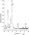
- AIN This piezoelectric material has been used for several years to fabricate FBARs (Film Bulk Acustic-wave Resonator) and energy scavengers. AIN is used as seed layer to grow ZnO NSs which will conform a functional nanostructured piezoelectric layer. AIN is processed by RF sputtering on top of a thin layer of Ti/Pt which infers a good crystalline orientation. Thin layers of less than 100 nm can be deposited and XRD analysis of Figure 4 shows that the crystalline structure and orientation are stable. The final thicknesses used in this type of devices may be between 10 nm and 1 um.
- ZnO This piezoelectric and semiconductor material will be used to grow nanostructures, specifically on piezoelectric ZnO nanowires (NWs) and nanosheets (NSs). ZnO NGs have been used for energy harvesting in the last years. These nanostructures have the advantages of being more flexible, less sensitive to fracture, and can be actuated easier than thin-films.
- the growth method is based on a hydrothermal chemical reaction at low temperature ( ⁇ 80° C) directly on the silicon substrate covered by a seed layer. This growth method is especially fast, easy, inexpensive and fully compatible with wafer-level silicon-based microelectronics technologies.
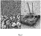
- Figure 2 shows the two types of ZnO nanostructures that will be used to fabricate the devices.
- a thin layer of AIN (thickness can be smaller than ⁇ 100nm) is used as seed layer, anti-screening carrier barrier and additional piezoelectric material.
- the thin layer of AIN should not affect the mechanical properties of the device because the created stress scales down with the thickness.
- the growth method for ZnO NSs is the same as for the NWs, but a different seed layer is used totally affecting the grown nanostructure shape. The main point that makes this nanostructure a promising solution for NG is the high uniformity, reproducibility and rapidness of the NS growth.
- Figure 3 shows the result of a Selected Area Electron Diffraction (SAED) generated in a TEM of a single NS layer were a high crystallinity of the material can be noticed. It can be also observed in Figure 3 that the growth direction is perpendicular to the c-axis, in contrast to a typical ZnO NW which grows along the c-axis. In case of NS, it can be observed a (0001) preferential growth plane at the expense of the inhibition of ⁇ 1010 ⁇ the growth plane, which is fully inverse in case of NW. Moreover, the hexagonal size of the ZnO crystals, typical of a wurtzite lattice, is clear. The hexagonal crystal can have a diameter of more than 1-5 ⁇ m and a thickness of less than 20 nm which means a huge aspect ratio larger than 100.
- SAED Selected Area Electron Diffraction
- a capacitor and a diode will be integrated together with the energy harvester in order to have a compact system able to get a DC voltage from a variable input acceleration.
- the fabrication process is addressed to be compatible with low demanding CMOS technologies.
- the final device is a released tip-loaded piezoelectric cantilever beam with integrated capacitor and diode as shown in Figure 5 .
- This integration allows reduced power losses and eases the combination of several generators without the need of controlling the phase differences of the generated piezopotentials (i.e. no resonant motion synchronization is necessary).
- a power output of 1.45 mW/cm 2 (for transduction area of ⁇ 4 mm 2 ) has been reported for a structure similar to the one which will be placed on top of the integrated capacitor for pressure levels similar to the achieved with the cantilever beam bending.
- a target output power of 500 ⁇ W/cm 2 is a reasonable value.
- NSs no previous data is available, but comparable power densities are expected because of the similar dimensions and crystal configuration of both NWs and NSs.
- the dimensions of the final devices will be 0.5x0.5x0.05 cm 3 , and they will be based on an n-type SOI wafer.
- a frame or holder made of glass or silicon is expected to be used in order to allow the inertial mass to move up and down. This support frame could increase the thickness of the final device by 0.05 cm.
Landscapes
- Chemical & Material Sciences (AREA)
- Engineering & Computer Science (AREA)
- Composite Materials (AREA)
- Materials Engineering (AREA)
- Piezo-Electric Or Mechanical Vibrators, Or Delay Or Filter Circuits (AREA)
- General Electrical Machinery Utilizing Piezoelectricity, Electrostriction Or Magnetostriction (AREA)
- Micromachines (AREA)
Abstract
Description
- The present invention belongs to the field of electronics and, more specifically, to nanoscale piezoelectric devices for harvesting mechanical energy.
- There is a need for electrical generators that are capable of providing power with high impact resistance and quality factor.
- Prior MEMS devices (MEMS stands for microelectromechanical systems) use standard AIN thin-film and have disadvantages of having a limited critical fracture stress and significant rigidity that make them not optimum for ambient vibration applications. Moreover, so far, they required external control and power management circuitry that makes difficult their integration and large scale manufacturing.
- Recently, it was proposed an approach based on piezoelectric nanofibres. Nevertheless this prior device has several disadvantages: low fibre surface density, low integration capability, difficult to obtain a large number of aligned fibers, substrate contamination due to nitration/oxidation of fibres. In addition, it requires a complex technological development (electro-spinning). Also, this device is less compatible with VLSI (Very large Scale Integration) silicon technologies.
- ZnO nanowires have being used as piezoelectric material in the last years, because they can be grown in an economic and easy way by hydrothermal method. Main application has been energy harvesting and sensors, but the devices have been mainly bulky macroscopic devices dedicated to generate as much power as possible. However, MEMS technology has not been exploited to successfully combine these nanostructures with micro-scale movable devices to target the small energy niche offered by ambient vibrations.
-
US20050134149A1 proposes a piezoelectric vibration harvesting device having a cymbal stack structure with a proof mass on top. This proposal is different to the present invention, in addition to its layout, in that the proposed invention uses ZnO nanostructures as main piezoelectric material instead of thin-films. In addition, the devices according to the invention can monolithically integrate diodes and capacitors. - The invention is devoted to develop a silicon-friendly family of piezoelectric nanostructured devices with integrated rectification and buffer charge-storage capacitor able to harvest energy from mechanical motions.
- According to the invention, a piezoelectric energy harvesting device comprises an anchored part, an inertial mass and a movable flexible structure. The flexible structure comprises a piezoelectric layer with a plurality of nanostructures. A capacitor is formed between a bottom electrode of a highly doped region and a top electrode of a metal layer and a diode is formed between the said metal layer and a lightly doped region in the anchored part, the diode is in-series with the capacitor.
- Preferably, the flexible structure is a cantilever beam between the anchored part and the inertial mass however other movable structures are possible. For instance, a clamped-clamped beam, a serpentine suspension, a membrane or other elastic element that can play the role of spring.
- The cantilever beam is designed to bend thereby causing the piezoelectric nanostructures to generate a piezopotential-driven current rectified by the diode and stored by the capacitor.
- Preferably, a seed layer comprising Au is formed under the piezoelectric layer made of ZnO to grow nanowires as nanostructures. Preferably, the length of nanowires is from 100 nm to 10 µm.
- Alternatively, a seed layer comprising AIN is formed under the piezoelectric layer made of ZnO to grow nanosheets as nanostructures. Preferably, the diameter of nanosheets rates from 100 nm to 10 µm.
- The electrodes of the capacitor extend from the cantilever beam to the anchored part but, preferably they can be extended to cover the entire available die surface to maximize the capacitance value.
- Preferably, the substrate material is n-type crystalline silicon.
- Alternatively, the substrate material is p-type crystalline silicon.
- According to the invention, an energy harvesting system is also proposed. The system comprises an array of piezoelectric energy harvesting devices, wherein neighboring devices are stacked by leaving a gap in between for the motion of the inertial mass. Preferably, the energy harvesting devices are combined in-series.
- Alternatively, the energy harvesting devices are combined in-parallel.
- In sum, a new approach is proposed to produce piezoelectric MEMS energy harvesters also referred to as scavengers MEMS. The proposed devices are based on nanowires (NWs) and nanosheets (NSs) as piezoelectric material with a monolithically integrated diode and capacitor in a silicon-friendly technology.
- In some embodiments ZnO is chosen as a low-cost solution to grow NWs and NSs by hydrothermal method. ZnO also provides a higher supported stress, enhanced flexibility and reduced manufacturing cost. At the same time, it is much easier to integrate with silicon than other nanostructure-based approaches. The device allows an out-of-plane motion when mechanically excited.
- The proposed energy harvesting device contains a Schottky diode and capacitor monolithically integrated besides the piezoelectric nanogenerator which allow an in-situ signal rectification and buffer charge storage.
- Positively, several energy harvesting devices can be combined to maximize the extracted power without concerns about AC output signal phases. The trade-off between size and number of energy harvesting devices shows that several smaller devices targeting different resonance frequencies can get higher generated power density than a bigger single unit with the same overall size.
- The invention has further advantages: an overall higher flexibility and lower fracture risk, better performance and integrated rectification and storage. This combination of power output with reliability improves the known state of the art devices.
- These and other aspects of the invention will become apparent from the drawings and exemplary embodiments.
- A series of drawings which aid in better understanding the invention and which are expressly related with embodiments of said invention, presented as a non-limiting example thereof, are very briefly described below.
-
Figure 1 : Functional device configuration. (Left) A cantilever structure for mechanical out-of-plane motions, with the two different ZnO nanostructures for piezoelectric transduction: nanowires (right-down) and nanosheets (right-up) -
Figure 2 : Several views of ZnO nanowires.Figure 2a is an overall view.Figure 2b is a detailed view.Figure 2c shows a top view of nanosheets.Figure 2d shows a tilted view. -
Figure 3 is an Scanning Electron Microscopy (SEM) image of ZnO NW grown over Au (left) and hexagonal ZnO nanosheets grown over AIN layer (center) and Selective Area Electron Diffraction (SAED) image corresponding to a single ZnO nanosheet generated by Transmission Electron Microscopy (TEM). -
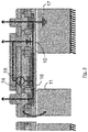
Figure 4 is an X-Ray Diffraction (XRD) measurement of ZnO nanosheets grown over an AIN seed layer. - Figure 5 is a cross section of the final device built on an SOI substrate.
- Several embodiments will be discussed for a better understanding of the invention.
- As indicated before, one of the goals of this invention is to make the energy harvester robust enough, able to work in a reliable way under the imposed conditions. For this purpose, piezoelectric nanostructures, also known in general as nanogenerators (NGs), are adopted instead of thin-films.
- The approach takes advantage of ZnO as transduction material to convert the mechanical energy coming from the input accelerations present in the environment for two different cases. Two types of ZnO nanostructures will be integrated to obtain usable devices: nanowires (NWs) and nanosheets (NSs).
- Both NWs and NSs can be generated sharing almost the same fabrication process: These ZnO nanostructures have the particularities of using:
- the whole die surface to manufacture the storage capacitor,
- the top electrode of this capacitor as seed layer to grow the ZnO nanostructures on top of the cantilever to be bent, and
- a small undoped silicon die region are to monolithically integrate Schottky diodes.
-
Figure 1 shows the configuration of one of the final devices. The common configuration of the different design versions is based on a cantilever architecture, because current silicon-based piezoelectric harvesters show the best performance with a spring-mass system. However, other suspensions, such as clamped-clamped beams, serpentine flexures, membranes or other elastic elements can be used instead of cantilever beam. -
Inertial mass 11 is connected through acantilever beam 16 to rest of the device die 13. On top of this cantilever, there is apiezoelectric layer 15 made of ZnO nanostructures. Monolithically integrated in thesame die 13, there is aSchottky diode 12 and acapacitor 14. - Several sizes will be generated to get different resonance frequencies, and combined to obtain multifrequency arrays of energy harvesters. The typical lateral dimensions of the cantilevers and inertial mass will rate from 0.5 to 5 mm, and the target thickness of the piezoelectric layer will be around 1 µm for the first prototype. The harvesters can be combined to produce an array according to series or parallel combination of them. Depending on this electrical combination, increment of output current or voltage levels will be obtained for series and parallel combinations respectively. In order to physically combine the devices, they can be stacked by leaving enough space in between for the inertial mass resonant motion.
- As illustrated in Figure 5, the spring is built by means of silicon beams microstructured on the SOI device layer and covered by the different piezoelectric material that plays the role of mechanical spring and transductor. The
inertial mass 11 is created by etching both top and bottom silicon layer of the SOI (Silicon On Insulator) wafer by RIE (Reactive Ion Etching) and DRIE (Deep Reactive Ion Etching) respectively. The non-etched part which corresponds to the frame off the die that will form the anchoredpart 17. - The use of an SOI wafer, eases the definition of
cantilever beam 16 and theinertial mass 11. This wafer will be n-type in order to be able of integrating aSchottky diode 12 and acapacitor 14 together with the movable structure. Thediode 12 will have the role of rectifying, with low losses, the AC signal generated by the NGs which at the same time will be grown just on top of the large surface of thecapacitor 14 to save area. - This configuration creates a network of a
diode 12,piezoelectric AC layer 15 as generator and acapacitor 14 in series, therefore for each mechanical stimulation on the NGs, negative charges will be stored in thecapacitor 14. Due to the in-situ rectification, different designs with different sizes can be connected together and the voltage output will be always added. For instance,longer cantilever 13 and/or biggerinertial masses 11 will result on lower resonance frequencies and thicker beams and/or stiffer materials will increases the resonance frequencies. - These devices use an SOI wafer as main structural part. The substrate is chosen in order to facilitate the inertial mass and beam definitions. Then two different piezoelectric materials are used:
AIN: This piezoelectric material has been used for several years to fabricate FBARs (Film Bulk Acustic-wave Resonator) and energy scavengers. AIN is used as seed layer to grow ZnO NSs which will conform a functional nanostructured piezoelectric layer. AIN is processed by RF sputtering on top of a thin layer of Ti/Pt which infers a good crystalline orientation. Thin layers of less than 100 nm can be deposited and XRD analysis ofFigure 4 shows that the crystalline structure and orientation are stable. The final thicknesses used in this type of devices may be between 10 nm and 1 um. - ZnO: This piezoelectric and semiconductor material will be used to grow nanostructures, specifically on piezoelectric ZnO nanowires (NWs) and nanosheets (NSs). ZnO NGs have been used for energy harvesting in the last years. These nanostructures have the advantages of being more flexible, less sensitive to fracture, and can be actuated easier than thin-films. The growth method is based on a hydrothermal chemical reaction at low temperature (< 80° C) directly on the silicon substrate covered by a seed layer. This growth method is especially fast, easy, inexpensive and fully compatible with wafer-level silicon-based microelectronics technologies.
-
Figure 2 shows the two types of ZnO nanostructures that will be used to fabricate the devices. - For the case of NSs, a thin layer of AIN (thickness can be smaller than <100nm) is used as seed layer, anti-screening carrier barrier and additional piezoelectric material. In this way, the thin layer of AIN should not affect the mechanical properties of the device because the created stress scales down with the thickness. The growth method for ZnO NSs is the same as for the NWs, but a different seed layer is used totally affecting the grown nanostructure shape. The main point that makes this nanostructure a promising solution for NG is the high uniformity, reproducibility and rapidness of the NS growth.
- Several studies have been carried out in order to verify that ZnO NSs grown over AIN have a good crystallinity and therefore piezoelectric properties.
-
Figure 3 shows the result of a Selected Area Electron Diffraction (SAED) generated in a TEM of a single NS layer were a high crystallinity of the material can be noticed. It can be also observed inFigure 3 that the growth direction is perpendicular to the c-axis, in contrast to a typical ZnO NW which grows along the c-axis. In case of NS, it can be observed a (0001) preferential growth plane at the expense of the inhibition of {1010} the growth plane, which is fully inverse in case of NW. Moreover, the hexagonal size of the ZnO crystals, typical of a wurtzite lattice, is clear. The hexagonal crystal can have a diameter of more than 1-5 µm and a thickness of less than 20 nm which means a huge aspect ratio larger than 100. - A XRD study was also performed to observe other crystalline orientations present in a matrix of NSs. The result can be seen in
Figure 4 . An outstanding peak can be observed for the desired (002) orientation of the ZnO, also the contribution of the AIN thin film is clearly visible. - As already mentioned, a capacitor and a diode will be integrated together with the energy harvester in order to have a compact system able to get a DC voltage from a variable input acceleration. The fabrication process is addressed to be compatible with low demanding CMOS technologies.
- The process steps to be followed to carry out the technological fabrication, including seven photolithographic steps, are listed below:
- 1. An n+ implantation is performed in selected areas of the n-doped SOI device layer through a protection oxide previously grown. This implantation will define the Ohmic contact with silicon and the bottom electrode of the capacitor. (N+ mask)
- 2. A field oxidation of 1060 nm is carried out in order to passivate the different devices. By means of Reactive Ion Etching (RIE) and wet etch this oxide can be selectively removed to define active regions. (Active area mask)
- 3. Performing of gate oxidation of 365 Å at 950 °C to create the thin oxide layer needed to make the capacitor.
- 4. Removing this thin oxide through dry and wet etches from contact areas to allow electrical access to the different contacts. (Contact mask)
- 5. On top of these contact areas, a multilayer of Cr/Ni/Au will be sputtered to create the capacitor top electrode, the metal-semiconductor interface of the Schottky diode and the metallic contacts. The capacitor electrode can be designed to cover the entire available die surface to maximize its charge capacity which is a great improvement compared to state-of-the-art devices. The last exposed Au layer will be also used as seed layer to grow ZnO NWs.
- 6. In order to fabricate the version of this device based on ZnO NS, a Ti/Pt layer followed by an AIN layer of 100 nm will be deposited by RF sputtering to generate the seed layer for these nanostructures.
- 7. The total metal stack and seed layer when applicable, is etched afterwards in selected areas. (Metal1 mask)
- 8. ZnO nanowires and nanosheets will be grown by a hydrothermal process on the respective seed layers deposited over capacitor top electrode which makes this device unique.
- 9. A layer of polymer (e.g. PMMA, PDMS or SU8), will be spin coated over the surface and developed to embed the NWs/NSs to avoid short-circuits between NG electrodes, if needed.
- 10. A thick layer of aluminum will be deposited (also other metals such as titanium and platinum can be used), patterned and etched to cover the embedded NWs/NSs, creating the upper NG electrode. (Metal2 mask).
- 11. The outline of the movable structures is patterned on the device side (RIE-front mask) and the SOI device layer is etched through by RIE.
- 12. On the back side, aluminum is deposited, patterned and etched to create a hard-mask for the DRIE. (DRIE-back mask).
- 13. The SOI handle wafer is fully etched by DRIE down to the buried oxide. A protective resist is coated on the front side before performing this step.
- 14. The structures are carefully released by wet etching of the SiO2 and the resist coating is dissolved by acetone immersion.
- The final device is a released tip-loaded piezoelectric cantilever beam with integrated capacitor and diode as shown in Figure 5. This integration allows reduced power losses and eases the combination of several generators without the need of controlling the phase differences of the generated piezopotentials (i.e. no resonant motion synchronization is necessary).
- For the device based on ZnO NWs, we take the assumption that the density of NWs will be ∼4 NW/µm2. If every NW takes an active part in the charge generation, and from a value of 4 pW/NW measured when a NW is bent by an AFM tip [4], it can be estimate a generated power of ∼1.6 mW/cm2. However, in our case the mechanical stimulation will be produced by the compression of the NW arrays derived from the beam bending and a typical transduction surface of 1 mm2. A power output of 1.45 mW/cm2 (for transduction area of ∼4 mm2) has been reported for a structure similar to the one which will be placed on top of the integrated capacitor for pressure levels similar to the achieved with the cantilever beam bending. Taking into account our device configuration (transduction area of ∼1 mm2, acceleration of 1-10 g, main stress of 1-10 MPa), a target output power of 500 µW/cm2 is a reasonable value. For the case of NSs, no previous data is available, but comparable power densities are expected because of the similar dimensions and crystal configuration of both NWs and NSs.
- From previous results, obtained by using similar structures but with a thin-film approach, we can estimate a lower limit value for our prototypes.
- For the first prototype, the dimensions of the final devices will be 0.5x0.5x0.05 cm3, and they will be based on an n-type SOI wafer. A frame or holder made of glass or silicon is expected to be used in order to allow the inertial mass to move up and down. This support frame could increase the thickness of the final device by 0.05 cm.
-
- 11 Inertial mass.
- 12 Schottky diode.
- 13 Device die.
- 14 Capacitor.
- 15 Piezoelectric layer.
- 16 Cantilever beam.
- 17 Anchored part.
Claims (12)
- A piezoelectric energy harvesting device, comprising:- an anchored part (17);- an inertial mass (11);- a flexible structure;characterized in that:- the flexible structure comprises a piezoelectric layer (15) with a plurality of nanostructures;- a capacitor (14) is formed between a bottom electrode of a heavy doped region and a top electrode of a metal layer; and- a diode (12) is formed between the said metal layer and a light doped region in the anchored part (17), the diode (12) is in-series with the capacitor (14),wherein the flexible structure is configured to bend thereby causing the piezoelectric nanostructures to generate a piezopotential-driven current rectified by the diode (12) and stored by the capacitor (14).
- The device according to claim 1, wherein the movable structure is a cantilever beam (16) between the anchored part (17) and the inertial mass (11).
- The device according to claim 1 or 2, wherein a seed layer comprising Au is formed under the piezoelectric layer (15) made of ZnO and the nanostructures are nanowires.
- The device according to claim 3, wherein the length of nanowires is from 100 nm to 10 µm.
- The device according to claim 1 or 2, wherein a seed layer comprising AIN is formed under the piezoelectric layer (15) made of ZnO and the nanostructures are nanosheets.
- The device according to claim 5, wherein the diameter of nanosheets rates from 100 nm to 10 µm.
- The device according to any of claims, wherein the electrodes of the capacitor (14) extends from the flexible structure to the anchored part (17).
- The device according to any of claims, wherein the substrate material is n-type crystalline silicon.
- The device according to any of claims 1 to 7, wherein the substrate material is p-type crystalline silicon.
- An energy harvesting system comprising an array of piezoelectric energy harvesting devices according to any of claims 1 to 9, wherein neighboring devices are stacked by leaving a gap in between for the motion of the inertial mass (11).
- The system according to claim 10, wherein the energy harvesting devices are combined in-series.
- The system according to claim 10, wherein the energy harvesting devices are combined in-parallel.
Applications Claiming Priority (2)
| Application Number | Priority Date | Filing Date | Title |
|---|---|---|---|
| ES201530896A ES2597983B1 (en) | 2015-06-24 | 2015-06-24 | Piezoelectric energy collection system and device |
| PCT/ES2016/070381 WO2016207458A1 (en) | 2015-06-24 | 2016-05-20 | System and device for collecting piezoelectric energy |
Publications (4)
| Publication Number | Publication Date |
|---|---|
| EP3319133A1 true EP3319133A1 (en) | 2018-05-09 |
| EP3319133A4 EP3319133A4 (en) | 2018-09-12 |
| EP3319133C0 EP3319133C0 (en) | 2023-09-20 |
| EP3319133B1 EP3319133B1 (en) | 2023-09-20 |
Family
ID=57584731
Family Applications (1)
| Application Number | Title | Priority Date | Filing Date |
|---|---|---|---|
| EP16813778.4A Active EP3319133B1 (en) | 2015-06-24 | 2016-05-20 | System and device for collecting piezoelectric energy |
Country Status (4)
| Country | Link |
|---|---|
| US (1) | US20200228032A1 (en) |
| EP (1) | EP3319133B1 (en) |
| ES (1) | ES2597983B1 (en) |
| WO (1) | WO2016207458A1 (en) |
Cited By (3)
| Publication number | Priority date | Publication date | Assignee | Title |
|---|---|---|---|---|
| EP3579290A1 (en) * | 2018-06-04 | 2019-12-11 | Shimco North America Inc. | 1d/2d hybrid piezoelectric nanogenerator and method for making same |
| WO2020258960A1 (en) * | 2019-06-26 | 2020-12-30 | 五邑大学 | Method for rapidly growing zno porous nano-film on the basis of hydrothermal process |
| EP4432546A1 (en) * | 2023-03-17 | 2024-09-18 | Cairdac | Energy harvester with piezoelectric transducer, in particular for supplying an autonomous cardiac capsule, with oscillating structure having a gradient of flexural stiffness |
Families Citing this family (2)
| Publication number | Priority date | Publication date | Assignee | Title |
|---|---|---|---|---|
| EP3351291B1 (en) * | 2017-01-20 | 2022-11-23 | Consejo Superior de Investigaciones Científicas (CSIC) | Self-generating voltage device for electrical cell stimulation, and method thereof |
| NL2028025B1 (en) * | 2021-04-21 | 2022-11-01 | Univ Delft Tech | A compliant structure |
Family Cites Families (3)
| Publication number | Priority date | Publication date | Assignee | Title |
|---|---|---|---|---|
| US20050134149A1 (en) * | 2003-07-11 | 2005-06-23 | Deng Ken K. | Piezoelectric vibration energy harvesting device |
| WO2012158914A1 (en) * | 2011-05-17 | 2012-11-22 | Georgia Tech Research Corporation | Nanogenerator for self-powered system with wireless data transmission |
| KR101906589B1 (en) * | 2011-08-30 | 2018-10-11 | 한국전자통신연구원 | Apparatus for Harvesting and Storaging Piezoelectric Energy and Manufacturing Method Thereof |
-
2015
- 2015-06-24 ES ES201530896A patent/ES2597983B1/en active Active
-
2016
- 2016-05-20 US US15/757,965 patent/US20200228032A1/en not_active Abandoned
- 2016-05-20 EP EP16813778.4A patent/EP3319133B1/en active Active
- 2016-05-20 WO PCT/ES2016/070381 patent/WO2016207458A1/en not_active Ceased
Cited By (5)
| Publication number | Priority date | Publication date | Assignee | Title |
|---|---|---|---|---|
| EP3579290A1 (en) * | 2018-06-04 | 2019-12-11 | Shimco North America Inc. | 1d/2d hybrid piezoelectric nanogenerator and method for making same |
| US12301139B2 (en) | 2018-06-04 | 2025-05-13 | Shimco North America Inc. | 1D/2D hybrid piezoelectric nanogenerator and method for making same |
| WO2020258960A1 (en) * | 2019-06-26 | 2020-12-30 | 五邑大学 | Method for rapidly growing zno porous nano-film on the basis of hydrothermal process |
| EP4432546A1 (en) * | 2023-03-17 | 2024-09-18 | Cairdac | Energy harvester with piezoelectric transducer, in particular for supplying an autonomous cardiac capsule, with oscillating structure having a gradient of flexural stiffness |
| US12255556B2 (en) | 2023-03-17 | 2025-03-18 | Cairdac | Piezoelectric-transducer energy harvester, in particular for powering an autonomous cardiac capsule, with a bending stiffness gradient oscillating structure |
Also Published As
| Publication number | Publication date |
|---|---|
| US20200228032A1 (en) | 2020-07-16 |
| ES2597983R2 (en) | 2017-02-28 |
| EP3319133C0 (en) | 2023-09-20 |
| ES2597983A2 (en) | 2017-01-24 |
| EP3319133B1 (en) | 2023-09-20 |
| WO2016207458A1 (en) | 2016-12-29 |
| EP3319133A4 (en) | 2018-09-12 |
| ES2597983B1 (en) | 2017-12-12 |
Similar Documents
| Publication | Publication Date | Title |
|---|---|---|
| EP3319133B1 (en) | System and device for collecting piezoelectric energy | |
| US12058938B2 (en) | MEMS piezoelectric device and corresponding manufacturing process | |
| US11228294B2 (en) | Graphene microelectromechanical system (MEMS) resonant gas sensor | |
| Liu et al. | A comprehensive review on piezoelectric energy harvesting technology: Materials, mechanisms, and applications | |
| EP2539946B1 (en) | High-efficiency mems micro-vibrational energy harvester and process for manufacturing same | |
| US8154176B2 (en) | System and method for resonance frequency tuning of resonant devices | |
| US20100084947A1 (en) | High Efficiency Piezoelectric Energy Harvester Having Spiral Structure | |
| Toprak et al. | Piezoelectric energy harvesting: State-of-the-art and challenges | |
| US9293689B2 (en) | Method of manufacturing a piezoelectric micro energy harvester | |
| US20130127295A1 (en) | Piezoelectric micro power generator and fabrication method thereof | |
| EP2036200A1 (en) | Semiconductor device transducer and method | |
| WO2011129855A9 (en) | Wide-bandwidth mems-scale piezoelectric energy harvesting device | |
| Reilly et al. | Thin film piezoelectric energy scavenging systems for long term medical monitoring | |
| WO2012164545A1 (en) | Energy scavenging from a rotating gear using an impact type piezoelectric mems scavenger | |
| Jambunathan et al. | Pulsed laser deposited-PZT based MEMS energy harvesting devices | |
| Kirubaveni et al. | Analysis of rectangular and triangular end array type piezoelectric vibration energy harvester | |
| Malki et al. | Wave energy harvesting system using piezocomposite materials | |
| US12212300B2 (en) | MEMS resonator with high quality factor and its use | |
| Abbasalipour et al. | High-energy density micro-machined cellular arrays of electrostatic actuators | |
| Kuwano | Piezoelectric tantalum aluminum nitride films for vibrational micro energy harvesters | |
| JP6199122B2 (en) | Vibration generator | |
| US20240010489A1 (en) | Mems device comprising a deformable structure and manufacturing process of the mems device | |
| US11713240B2 (en) | Cellular array electrostatic actuator | |
| KR20090112348A (en) | Micro piezoelectric generator and its manufacturing method | |
| Sordo et al. | Study on the effectiveness of different electrode geometries for sputtered aluminium nitride-based MEMS energy harvesters |
Legal Events
| Date | Code | Title | Description |
|---|---|---|---|
| STAA | Information on the status of an ep patent application or granted ep patent |
Free format text: STATUS: THE INTERNATIONAL PUBLICATION HAS BEEN MADE |
|
| PUAI | Public reference made under article 153(3) epc to a published international application that has entered the european phase |
Free format text: ORIGINAL CODE: 0009012 |
|
| STAA | Information on the status of an ep patent application or granted ep patent |
Free format text: STATUS: REQUEST FOR EXAMINATION WAS MADE |
|
| 17P | Request for examination filed |
Effective date: 20180305 |
|
| AK | Designated contracting states |
Kind code of ref document: A1 Designated state(s): AL AT BE BG CH CY CZ DE DK EE ES FI FR GB GR HR HU IE IS IT LI LT LU LV MC MK MT NL NO PL PT RO RS SE SI SK SM TR |
|
| AX | Request for extension of the european patent |
Extension state: BA ME |
|
| A4 | Supplementary search report drawn up and despatched |
Effective date: 20180816 |
|
| RIC1 | Information provided on ipc code assigned before grant |
Ipc: H01L 41/113 20060101AFI20180809BHEP |
|
| DAV | Request for validation of the european patent (deleted) | ||
| DAX | Request for extension of the european patent (deleted) | ||
| STAA | Information on the status of an ep patent application or granted ep patent |
Free format text: STATUS: EXAMINATION IS IN PROGRESS |
|
| 17Q | First examination report despatched |
Effective date: 20200408 |
|
| REG | Reference to a national code |
Ref country code: DE Ref legal event code: R079 Free format text: PREVIOUS MAIN CLASS: H01L0041113000 Ipc: H10N0030300000 Ref document number: 602016082913 Country of ref document: DE |
|
| GRAP | Despatch of communication of intention to grant a patent |
Free format text: ORIGINAL CODE: EPIDOSNIGR1 |
|
| STAA | Information on the status of an ep patent application or granted ep patent |
Free format text: STATUS: GRANT OF PATENT IS INTENDED |
|
| RIC1 | Information provided on ipc code assigned before grant |
Ipc: H10N 39/00 20230101ALI20230310BHEP Ipc: H10N 30/30 20230101AFI20230310BHEP |
|
| INTG | Intention to grant announced |
Effective date: 20230417 |
|
| GRAS | Grant fee paid |
Free format text: ORIGINAL CODE: EPIDOSNIGR3 |
|
| GRAA | (expected) grant |
Free format text: ORIGINAL CODE: 0009210 |
|
| STAA | Information on the status of an ep patent application or granted ep patent |
Free format text: STATUS: THE PATENT HAS BEEN GRANTED |
|
| AK | Designated contracting states |
Kind code of ref document: B1 Designated state(s): AL AT BE BG CH CY CZ DE DK EE ES FI FR GB GR HR HU IE IS IT LI LT LU LV MC MK MT NL NO PL PT RO RS SE SI SK SM TR |
|
| REG | Reference to a national code |
Ref country code: GB Ref legal event code: FG4D |
|
| REG | Reference to a national code |
Ref country code: CH Ref legal event code: EP |
|
| REG | Reference to a national code |
Ref country code: DE Ref legal event code: R096 Ref document number: 602016082913 Country of ref document: DE |
|
| REG | Reference to a national code |
Ref country code: IE Ref legal event code: FG4D |
|
| U01 | Request for unitary effect filed |
Effective date: 20231016 |
|
| U07 | Unitary effect registered |
Designated state(s): AT BE BG DE DK EE FI FR IT LT LU LV MT NL PT SE SI Effective date: 20231024 |
|
| PG25 | Lapsed in a contracting state [announced via postgrant information from national office to epo] |
Ref country code: GR Free format text: LAPSE BECAUSE OF FAILURE TO SUBMIT A TRANSLATION OF THE DESCRIPTION OR TO PAY THE FEE WITHIN THE PRESCRIBED TIME-LIMIT Effective date: 20231221 |
|
| PG25 | Lapsed in a contracting state [announced via postgrant information from national office to epo] |
Ref country code: RS Free format text: LAPSE BECAUSE OF FAILURE TO SUBMIT A TRANSLATION OF THE DESCRIPTION OR TO PAY THE FEE WITHIN THE PRESCRIBED TIME-LIMIT Effective date: 20230920 Ref country code: NO Free format text: LAPSE BECAUSE OF FAILURE TO SUBMIT A TRANSLATION OF THE DESCRIPTION OR TO PAY THE FEE WITHIN THE PRESCRIBED TIME-LIMIT Effective date: 20231220 Ref country code: HR Free format text: LAPSE BECAUSE OF FAILURE TO SUBMIT A TRANSLATION OF THE DESCRIPTION OR TO PAY THE FEE WITHIN THE PRESCRIBED TIME-LIMIT Effective date: 20230920 Ref country code: GR Free format text: LAPSE BECAUSE OF FAILURE TO SUBMIT A TRANSLATION OF THE DESCRIPTION OR TO PAY THE FEE WITHIN THE PRESCRIBED TIME-LIMIT Effective date: 20231221 |
|
| PG25 | Lapsed in a contracting state [announced via postgrant information from national office to epo] |
Ref country code: IS Free format text: LAPSE BECAUSE OF FAILURE TO SUBMIT A TRANSLATION OF THE DESCRIPTION OR TO PAY THE FEE WITHIN THE PRESCRIBED TIME-LIMIT Effective date: 20240120 |
|
| PG25 | Lapsed in a contracting state [announced via postgrant information from national office to epo] |
Ref country code: ES Free format text: LAPSE BECAUSE OF FAILURE TO SUBMIT A TRANSLATION OF THE DESCRIPTION OR TO PAY THE FEE WITHIN THE PRESCRIBED TIME-LIMIT Effective date: 20230920 |
|
| PG25 | Lapsed in a contracting state [announced via postgrant information from national office to epo] |
Ref country code: SM Free format text: LAPSE BECAUSE OF FAILURE TO SUBMIT A TRANSLATION OF THE DESCRIPTION OR TO PAY THE FEE WITHIN THE PRESCRIBED TIME-LIMIT Effective date: 20230920 Ref country code: RO Free format text: LAPSE BECAUSE OF FAILURE TO SUBMIT A TRANSLATION OF THE DESCRIPTION OR TO PAY THE FEE WITHIN THE PRESCRIBED TIME-LIMIT Effective date: 20230920 Ref country code: IS Free format text: LAPSE BECAUSE OF FAILURE TO SUBMIT A TRANSLATION OF THE DESCRIPTION OR TO PAY THE FEE WITHIN THE PRESCRIBED TIME-LIMIT Effective date: 20240120 Ref country code: ES Free format text: LAPSE BECAUSE OF FAILURE TO SUBMIT A TRANSLATION OF THE DESCRIPTION OR TO PAY THE FEE WITHIN THE PRESCRIBED TIME-LIMIT Effective date: 20230920 Ref country code: CZ Free format text: LAPSE BECAUSE OF FAILURE TO SUBMIT A TRANSLATION OF THE DESCRIPTION OR TO PAY THE FEE WITHIN THE PRESCRIBED TIME-LIMIT Effective date: 20230920 Ref country code: SK Free format text: LAPSE BECAUSE OF FAILURE TO SUBMIT A TRANSLATION OF THE DESCRIPTION OR TO PAY THE FEE WITHIN THE PRESCRIBED TIME-LIMIT Effective date: 20230920 |
|
| PG25 | Lapsed in a contracting state [announced via postgrant information from national office to epo] |
Ref country code: PL Free format text: LAPSE BECAUSE OF FAILURE TO SUBMIT A TRANSLATION OF THE DESCRIPTION OR TO PAY THE FEE WITHIN THE PRESCRIBED TIME-LIMIT Effective date: 20230920 |
|
| REG | Reference to a national code |
Ref country code: DE Ref legal event code: R097 Ref document number: 602016082913 Country of ref document: DE |
|
| U20 | Renewal fee for the european patent with unitary effect paid |
Year of fee payment: 9 Effective date: 20240522 |
|
| PLBE | No opposition filed within time limit |
Free format text: ORIGINAL CODE: 0009261 |
|
| STAA | Information on the status of an ep patent application or granted ep patent |
Free format text: STATUS: NO OPPOSITION FILED WITHIN TIME LIMIT |
|
| 26N | No opposition filed |
Effective date: 20240621 |
|
| REG | Reference to a national code |
Ref country code: CH Ref legal event code: PL |
|
| PG25 | Lapsed in a contracting state [announced via postgrant information from national office to epo] |
Ref country code: MC Free format text: LAPSE BECAUSE OF FAILURE TO SUBMIT A TRANSLATION OF THE DESCRIPTION OR TO PAY THE FEE WITHIN THE PRESCRIBED TIME-LIMIT Effective date: 20230920 |
|
| GBPC | Gb: european patent ceased through non-payment of renewal fee |
Effective date: 20240520 |
|
| PG25 | Lapsed in a contracting state [announced via postgrant information from national office to epo] |
Ref country code: MC Free format text: LAPSE BECAUSE OF FAILURE TO SUBMIT A TRANSLATION OF THE DESCRIPTION OR TO PAY THE FEE WITHIN THE PRESCRIBED TIME-LIMIT Effective date: 20230920 Ref country code: CH Free format text: LAPSE BECAUSE OF NON-PAYMENT OF DUE FEES Effective date: 20240531 |
|
| PG25 | Lapsed in a contracting state [announced via postgrant information from national office to epo] |
Ref country code: IE Free format text: LAPSE BECAUSE OF NON-PAYMENT OF DUE FEES Effective date: 20240520 |
|
| PG25 | Lapsed in a contracting state [announced via postgrant information from national office to epo] |
Ref country code: GB Free format text: LAPSE BECAUSE OF NON-PAYMENT OF DUE FEES Effective date: 20240520 |
|
| U21 | Renewal fee for the european patent with unitary effect paid with additional fee |
Year of fee payment: 10 Effective date: 20250605 |
|
| PG25 | Lapsed in a contracting state [announced via postgrant information from national office to epo] |
Ref country code: CY Free format text: LAPSE BECAUSE OF FAILURE TO SUBMIT A TRANSLATION OF THE DESCRIPTION OR TO PAY THE FEE WITHIN THE PRESCRIBED TIME-LIMIT; INVALID AB INITIO Effective date: 20160520 |
|
| PG25 | Lapsed in a contracting state [announced via postgrant information from national office to epo] |
Ref country code: HU Free format text: LAPSE BECAUSE OF FAILURE TO SUBMIT A TRANSLATION OF THE DESCRIPTION OR TO PAY THE FEE WITHIN THE PRESCRIBED TIME-LIMIT; INVALID AB INITIO Effective date: 20160520 |