EP2539946B1 - High-efficiency mems micro-vibrational energy harvester and process for manufacturing same - Google Patents
High-efficiency mems micro-vibrational energy harvester and process for manufacturing same Download PDFInfo
- Publication number
- EP2539946B1 EP2539946B1 EP11747905.5A EP11747905A EP2539946B1 EP 2539946 B1 EP2539946 B1 EP 2539946B1 EP 11747905 A EP11747905 A EP 11747905A EP 2539946 B1 EP2539946 B1 EP 2539946B1
- Authority
- EP
- European Patent Office
- Prior art keywords
- vibrational energy
- energy harvesting
- harvesting device
- layer
- recited
- Prior art date
- Legal status (The legal status is an assumption and is not a legal conclusion. Google has not performed a legal analysis and makes no representation as to the accuracy of the status listed.)
- Not-in-force
Links
- 238000000034 method Methods 0.000 title claims description 29
- 238000004519 manufacturing process Methods 0.000 title claims description 14
- 230000008569 process Effects 0.000 title description 19
- 239000010410 layer Substances 0.000 claims description 107
- 239000000463 material Substances 0.000 claims description 34
- 238000003306 harvesting Methods 0.000 claims description 23
- 229910052710 silicon Inorganic materials 0.000 claims description 16
- 239000010703 silicon Substances 0.000 claims description 16
- 239000000758 substrate Substances 0.000 claims description 11
- 238000000151 deposition Methods 0.000 claims description 9
- PCHJSUWPFVWCPO-UHFFFAOYSA-N gold Chemical group [Au] PCHJSUWPFVWCPO-UHFFFAOYSA-N 0.000 claims description 6
- 229910052737 gold Inorganic materials 0.000 claims description 6
- 239000010931 gold Substances 0.000 claims description 6
- 238000005530 etching Methods 0.000 claims description 5
- PMHQVHHXPFUNSP-UHFFFAOYSA-M copper(1+);methylsulfanylmethane;bromide Chemical compound Br[Cu].CSC PMHQVHHXPFUNSP-UHFFFAOYSA-M 0.000 claims description 4
- 239000007789 gas Substances 0.000 claims description 4
- RYGMFSIKBFXOCR-UHFFFAOYSA-N Copper Chemical group [Cu] RYGMFSIKBFXOCR-UHFFFAOYSA-N 0.000 claims description 3
- 229910052802 copper Inorganic materials 0.000 claims description 3
- 239000010949 copper Substances 0.000 claims description 3
- 239000012792 core layer Substances 0.000 claims description 3
- 238000007747 plating Methods 0.000 claims description 3
- 239000011261 inert gas Substances 0.000 claims description 2
- 238000000059 patterning Methods 0.000 claims 5
- PXHVJJICTQNCMI-UHFFFAOYSA-N Nickel Chemical group [Ni] PXHVJJICTQNCMI-UHFFFAOYSA-N 0.000 claims 2
- 229910052759 nickel Inorganic materials 0.000 claims 1
- 239000010408 film Substances 0.000 description 32
- 235000012431 wafers Nutrition 0.000 description 26
- 230000007935 neutral effect Effects 0.000 description 25
- XUIMIQQOPSSXEZ-UHFFFAOYSA-N Silicon Chemical compound [Si] XUIMIQQOPSSXEZ-UHFFFAOYSA-N 0.000 description 15
- 241001124569 Lycaenidae Species 0.000 description 12
- 230000007613 environmental effect Effects 0.000 description 12
- 239000010409 thin film Substances 0.000 description 12
- 238000012545 processing Methods 0.000 description 10
- VYPSYNLAJGMNEJ-UHFFFAOYSA-N Silicium dioxide Chemical compound O=[Si]=O VYPSYNLAJGMNEJ-UHFFFAOYSA-N 0.000 description 8
- 230000005611 electricity Effects 0.000 description 7
- 238000013459 approach Methods 0.000 description 6
- 238000004377 microelectronic Methods 0.000 description 6
- 238000012544 monitoring process Methods 0.000 description 6
- 238000000623 plasma-assisted chemical vapour deposition Methods 0.000 description 6
- 239000004065 semiconductor Substances 0.000 description 6
- 238000005452 bending Methods 0.000 description 5
- 230000008021 deposition Effects 0.000 description 5
- 125000006850 spacer group Chemical group 0.000 description 5
- 230000008901 benefit Effects 0.000 description 4
- 239000004020 conductor Substances 0.000 description 4
- 230000005684 electric field Effects 0.000 description 4
- 238000004806 packaging method and process Methods 0.000 description 4
- BASFCYQUMIYNBI-UHFFFAOYSA-N platinum Chemical compound [Pt] BASFCYQUMIYNBI-UHFFFAOYSA-N 0.000 description 4
- 235000012239 silicon dioxide Nutrition 0.000 description 4
- 239000000377 silicon dioxide Substances 0.000 description 4
- ZOKXTWBITQBERF-UHFFFAOYSA-N Molybdenum Chemical compound [Mo] ZOKXTWBITQBERF-UHFFFAOYSA-N 0.000 description 3
- 230000001133 acceleration Effects 0.000 description 3
- 238000007906 compression Methods 0.000 description 3
- 238000006073 displacement reaction Methods 0.000 description 3
- 238000004146 energy storage Methods 0.000 description 3
- 150000002500 ions Chemical class 0.000 description 3
- 229910052451 lead zirconate titanate Inorganic materials 0.000 description 3
- HFGPZNIAWCZYJU-UHFFFAOYSA-N lead zirconate titanate Chemical compound [O-2].[O-2].[O-2].[O-2].[O-2].[Ti+4].[Zr+4].[Pb+2] HFGPZNIAWCZYJU-UHFFFAOYSA-N 0.000 description 3
- 229910052750 molybdenum Inorganic materials 0.000 description 3
- 239000011733 molybdenum Substances 0.000 description 3
- 238000004544 sputter deposition Methods 0.000 description 3
- 239000000126 substance Substances 0.000 description 3
- KRHYYFGTRYWZRS-UHFFFAOYSA-N Fluorane Chemical compound F KRHYYFGTRYWZRS-UHFFFAOYSA-N 0.000 description 2
- XPDWGBQVDMORPB-UHFFFAOYSA-N Fluoroform Chemical compound FC(F)F XPDWGBQVDMORPB-UHFFFAOYSA-N 0.000 description 2
- DKNPRRRKHAEUMW-UHFFFAOYSA-N Iodine aqueous Chemical compound [K+].I[I-]I DKNPRRRKHAEUMW-UHFFFAOYSA-N 0.000 description 2
- 229910052581 Si3N4 Inorganic materials 0.000 description 2
- 238000004378 air conditioning Methods 0.000 description 2
- 238000000231 atomic layer deposition Methods 0.000 description 2
- 239000003990 capacitor Substances 0.000 description 2
- 239000000919 ceramic Substances 0.000 description 2
- 238000005229 chemical vapour deposition Methods 0.000 description 2
- 230000006835 compression Effects 0.000 description 2
- 238000013461 design Methods 0.000 description 2
- 239000007772 electrode material Substances 0.000 description 2
- 230000036541 health Effects 0.000 description 2
- 238000010438 heat treatment Methods 0.000 description 2
- 229910000040 hydrogen fluoride Inorganic materials 0.000 description 2
- 239000012212 insulator Substances 0.000 description 2
- 230000033001 locomotion Effects 0.000 description 2
- 238000004518 low pressure chemical vapour deposition Methods 0.000 description 2
- 230000000873 masking effect Effects 0.000 description 2
- 230000003534 oscillatory effect Effects 0.000 description 2
- 230000003647 oxidation Effects 0.000 description 2
- 238000007254 oxidation reaction Methods 0.000 description 2
- 229920002120 photoresistant polymer Polymers 0.000 description 2
- 238000005240 physical vapour deposition Methods 0.000 description 2
- 229910052697 platinum Inorganic materials 0.000 description 2
- 230000001681 protective effect Effects 0.000 description 2
- HQVNEWCFYHHQES-UHFFFAOYSA-N silicon nitride Chemical compound N12[Si]34N5[Si]62N3[Si]51N64 HQVNEWCFYHHQES-UHFFFAOYSA-N 0.000 description 2
- 238000000427 thin-film deposition Methods 0.000 description 2
- 238000007738 vacuum evaporation Methods 0.000 description 2
- 239000011800 void material Substances 0.000 description 2
- XLYOFNOQVPJJNP-UHFFFAOYSA-N water Substances O XLYOFNOQVPJJNP-UHFFFAOYSA-N 0.000 description 2
- PIGFYZPCRLYGLF-UHFFFAOYSA-N Aluminum nitride Chemical compound [Al]#N PIGFYZPCRLYGLF-UHFFFAOYSA-N 0.000 description 1
- JBRZTFJDHDCESZ-UHFFFAOYSA-N AsGa Chemical compound [As]#[Ga] JBRZTFJDHDCESZ-UHFFFAOYSA-N 0.000 description 1
- 206010065929 Cardiovascular insufficiency Diseases 0.000 description 1
- 229910001218 Gallium arsenide Inorganic materials 0.000 description 1
- 230000005483 Hooke's law Effects 0.000 description 1
- 239000002033 PVDF binder Substances 0.000 description 1
- 239000003570 air Substances 0.000 description 1
- 229910052782 aluminium Inorganic materials 0.000 description 1
- XAGFODPZIPBFFR-UHFFFAOYSA-N aluminium Chemical compound [Al] XAGFODPZIPBFFR-UHFFFAOYSA-N 0.000 description 1
- 239000012080 ambient air Substances 0.000 description 1
- QVGXLLKOCUKJST-UHFFFAOYSA-N atomic oxygen Chemical compound [O] QVGXLLKOCUKJST-UHFFFAOYSA-N 0.000 description 1
- JRPBQTZRNDNNOP-UHFFFAOYSA-N barium titanate Chemical compound [Ba+2].[Ba+2].[O-][Ti]([O-])([O-])[O-] JRPBQTZRNDNNOP-UHFFFAOYSA-N 0.000 description 1
- 229910002113 barium titanate Inorganic materials 0.000 description 1
- 229910052797 bismuth Inorganic materials 0.000 description 1
- JCXGWMGPZLAOME-UHFFFAOYSA-N bismuth atom Chemical compound [Bi] JCXGWMGPZLAOME-UHFFFAOYSA-N 0.000 description 1
- 238000005234 chemical deposition Methods 0.000 description 1
- 239000011248 coating agent Substances 0.000 description 1
- 238000000576 coating method Methods 0.000 description 1
- 238000010276 construction Methods 0.000 description 1
- 238000005520 cutting process Methods 0.000 description 1
- 238000013016 damping Methods 0.000 description 1
- 230000007547 defect Effects 0.000 description 1
- 230000007123 defense Effects 0.000 description 1
- 238000011161 development Methods 0.000 description 1
- 238000009792 diffusion process Methods 0.000 description 1
- NKZSPGSOXYXWQA-UHFFFAOYSA-N dioxido(oxo)titanium;lead(2+) Chemical compound [Pb+2].[O-][Ti]([O-])=O NKZSPGSOXYXWQA-UHFFFAOYSA-N 0.000 description 1
- 238000004100 electronic packaging Methods 0.000 description 1
- 238000009713 electroplating Methods 0.000 description 1
- 238000001704 evaporation Methods 0.000 description 1
- 230000008020 evaporation Effects 0.000 description 1
- 238000007667 floating Methods 0.000 description 1
- 239000012530 fluid Substances 0.000 description 1
- 235000013305 food Nutrition 0.000 description 1
- -1 for example Substances 0.000 description 1
- 229910000154 gallium phosphate Inorganic materials 0.000 description 1
- 239000011521 glass Substances 0.000 description 1
- 230000005484 gravity Effects 0.000 description 1
- 239000007943 implant Substances 0.000 description 1
- 238000009413 insulation Methods 0.000 description 1
- 230000000670 limiting effect Effects 0.000 description 1
- 229910052751 metal Inorganic materials 0.000 description 1
- 239000002184 metal Substances 0.000 description 1
- 229910044991 metal oxide Inorganic materials 0.000 description 1
- 150000004706 metal oxides Chemical class 0.000 description 1
- 238000001465 metallisation Methods 0.000 description 1
- 239000000203 mixture Substances 0.000 description 1
- 238000001451 molecular beam epitaxy Methods 0.000 description 1
- 229910021421 monocrystalline silicon Inorganic materials 0.000 description 1
- 150000004767 nitrides Chemical class 0.000 description 1
- 239000000615 nonconductor Substances 0.000 description 1
- 230000003287 optical effect Effects 0.000 description 1
- 239000001301 oxygen Substances 0.000 description 1
- 229910052760 oxygen Inorganic materials 0.000 description 1
- 230000010363 phase shift Effects 0.000 description 1
- 238000000206 photolithography Methods 0.000 description 1
- 238000005289 physical deposition Methods 0.000 description 1
- 229920002981 polyvinylidene fluoride Polymers 0.000 description 1
- BITYAPCSNKJESK-UHFFFAOYSA-N potassiosodium Chemical compound [Na].[K] BITYAPCSNKJESK-UHFFFAOYSA-N 0.000 description 1
- 239000002243 precursor Substances 0.000 description 1
- 230000002829 reductive effect Effects 0.000 description 1
- 230000004044 response Effects 0.000 description 1
- 230000002441 reversible effect Effects 0.000 description 1
- 230000035945 sensitivity Effects 0.000 description 1
- 239000002356 single layer Substances 0.000 description 1
- UYLYBEXRJGPQSH-UHFFFAOYSA-N sodium;oxido(dioxo)niobium Chemical compound [Na+].[O-][Nb](=O)=O UYLYBEXRJGPQSH-UHFFFAOYSA-N 0.000 description 1
- 238000001228 spectrum Methods 0.000 description 1
- 238000012546 transfer Methods 0.000 description 1
- 230000001052 transient effect Effects 0.000 description 1
- 238000009423 ventilation Methods 0.000 description 1
- 229910000859 α-Fe Inorganic materials 0.000 description 1
Images


Classifications
-
- H—ELECTRICITY
- H02—GENERATION; CONVERSION OR DISTRIBUTION OF ELECTRIC POWER
- H02N—ELECTRIC MACHINES NOT OTHERWISE PROVIDED FOR
- H02N2/00—Electric machines in general using piezoelectric effect, electrostriction or magnetostriction
- H02N2/18—Electric machines in general using piezoelectric effect, electrostriction or magnetostriction producing electrical output from mechanical input, e.g. generators
- H02N2/186—Vibration harvesters
- H02N2/188—Vibration harvesters adapted for resonant operation
-
- H—ELECTRICITY
- H10—SEMICONDUCTOR DEVICES; ELECTRIC SOLID-STATE DEVICES NOT OTHERWISE PROVIDED FOR
- H10N—ELECTRIC SOLID-STATE DEVICES NOT OTHERWISE PROVIDED FOR
- H10N30/00—Piezoelectric or electrostrictive devices
- H10N30/01—Manufacture or treatment
-
- H—ELECTRICITY
- H10—SEMICONDUCTOR DEVICES; ELECTRIC SOLID-STATE DEVICES NOT OTHERWISE PROVIDED FOR
- H10N—ELECTRIC SOLID-STATE DEVICES NOT OTHERWISE PROVIDED FOR
- H10N30/00—Piezoelectric or electrostrictive devices
- H10N30/30—Piezoelectric or electrostrictive devices with mechanical input and electrical output, e.g. functioning as generators or sensors
- H10N30/304—Beam type
- H10N30/306—Cantilevers
-
- Y—GENERAL TAGGING OF NEW TECHNOLOGICAL DEVELOPMENTS; GENERAL TAGGING OF CROSS-SECTIONAL TECHNOLOGIES SPANNING OVER SEVERAL SECTIONS OF THE IPC; TECHNICAL SUBJECTS COVERED BY FORMER USPC CROSS-REFERENCE ART COLLECTIONS [XRACs] AND DIGESTS
- Y10—TECHNICAL SUBJECTS COVERED BY FORMER USPC
- Y10T—TECHNICAL SUBJECTS COVERED BY FORMER US CLASSIFICATION
- Y10T29/00—Metal working
- Y10T29/42—Piezoelectric device making
Definitions
- the present invention relates generally to energy scavengers and energy harvesters which convert ambient forms of energy into electricity, and more particularly to vibrational energy harvesters that convert environmental mechanical vibrational energy to electrical energy utilizing piezoelectric type materials.
- Such apparatusses are inter alia known from the US 2005/280334 , WO 2008/116173 and US 2007/114890 .
- One of the most familiar types of energy harvester is the solar cell. Additionally, there are energy harvesters that convert thermal gradients, wind power, water power, and the like into electric power. To take advantage of these types of energy harvesters, environmental contact such as exposure to light, thermal gradients, wind, water, and the like is required. These types of energy harvesters are not commonly found in enclosed environmental spaces such as HVAC systems or walls, embedded in machinery or tissue, or other applications that do not have access to external environmental energy sources.
- vibrational type energy harvesters are able to take advantage of environmental vibrations created by appliances, HVAC (Heating Ventilating and Air-Conditioning) systems, equipment, motors, human movement, and the like, to produce electrical power or electricity in open as well as enclosed environmental spaces. These environmental vibrational frequencies are typically found in the 1-1000 Hz range.
- a VEH comprises a proof mass on a spring.
- the spring is typically a cantilever beam.
- the mass / spring combination has a resonant frequency and, although it can respond to a spectrum of vibrational frequencies, it responds most strongly to ambient vibrations around that resonant frequency. This resonant motion can be converted to electricity using techniques such as electromagnetic pick-up or piezoelectric generation.
- Wireless sensors measure environmental variables and transmit the measured data back to a receiver without any cabling or wires. Typically, the data is transmitted using radio frequency signals and the power for the sensor is provided by a battery, capacitor, or similar energy storage device. Wireless sensors have many potential applications because they can be used where it is difficult to get wires or as after-market system upgrades requiring no additional cabling. Some of the many applications that have been identified that could benefit from wireless sensors include:
- One solution to this wireless sensor power problem is to provide power using energy scavengers or energy harvesters which can convert ambient forms of energy into electricity for use by the sensor or for charging the battery.
- Microfabricated MEMS VEH devices may provide such a solution.
- ⁇ VEHs Microfabricated VEH Devices
- a piezoelectric MEMS ⁇ VEH consists of a cantilever beam element capped with a piezoelectric film and terminated with a proof mass.
- the mass stresses the cantilever beam, including the piezoelectric film.
- the stress in the piezoelectric film generates charge and a voltage difference is created across the capacitor formed by the piezoelectric between the top and bottom surfaces.
- ⁇ VEHs typically have high resonant frequencies (>500 Hz).
- the cantilever beam (spring) In order to achieve the desired low resonant frequency configuration and sensitivity, the cantilever beam (spring) must be long (a few mm), thin, and compliant, and the mass must be large (a few milligrams). For MEMS ⁇ VEHs, this is difficult. MEMS fabrication is based on thin film processing techniques developed by the semiconductor industry.
- Conducting, insulating, semiconductor, and piezoelectric films are deposited using sputtering, vacuum evaporation, or chemical vapor deposition and are typically only 1-3 microns thick (or less).
- a 5 micron thick film is a very thick film deposition for a microfabrication process. It is relatively difficult to construct large structures with such thin film fabrication techniques.
- piezoelectric ⁇ VEHs produce voltages of only a few hundredths of a volt and power levels of only a few ⁇ W or less.
- One of the primary reasons for such low outputs is the limited stress that can be applied to the piezoelectric element. It is known in the art that the stress in a bending cantilever beam element is proportional to the distance of the element from the neutral axis of the cantilever. The neutral axis is defined as the line where the stress is zero. When the cantilever bends downward, the stress above the neutral axis is tensile. Below the neutral axis, it is compressive. When it bends upward, the stresses reverse.
- the easiest way to get the entire piezoelectric film away from the neutral axis is to deposit it on a base. This is commonly achieved by placing the thin piezoelectric film on a thicker silicon (Si) or silicon dioxide mechanical cantilever.
- Si silicon
- This single element, or monomorph, architecture can be fabricated several ways. One way is to deposit the mechanical base layer on a standard Si wafer prior to deposition of the piezoelectric and electrode films. This base layer must be relatively thick (in microelectronics terms), for example, 3-5 microns thick. Even so, the neutral axis will be just inside or just below the piezoelectric.
- a second approach is to use a silicon-on-insulator (SOI) wafer that has a single crystal silicon layer a few microns thick atop a buried oxide layer which again is atop a thick handle.
- SOI silicon-on-insulator
- a second limitation of the MEMS monomorph architecture is that the mechanical energy that drives the cantilever must be shared between bending the support cantilever and bending the piezoelectric element. The energy that is required to bend the support does not go into straining the piezoelectric, thereby limiting the amount of voltage that can be developed.
- AlN Aluminum nitride
- Mo common electrode material
- a vibrational energy harvesting device comprising a cantilever having a first end, a second end and a core having a first planar surface and a second planar surface, the core being fabricated as two plate layers and bonded together; a first piezoelectric stack having a piezoelectric material placed between a first conductive layer and a second conductive layer and attached to the first planar surface of said core; a second piezoelectric stack having a piezoelectric material placed between a first conductive layer and a second conductive layer and attached to the second planar surface of said core; and a casing wherein the first end of the cantilever is joined to the casing and the second end is free to move.
- MEMS Micro-Electro-Mechanical Systems.
- MEMS are integrated circuits (ICs) manufactured using processes and equipment similar to that used in the microelectronics industry.
- MEMS ICs include mechanical, fluidic, or optical elements in addition to electrical circuits.
- MEMS ICs are used for applications such as miniature sensors and transducers.
- Piezoelectric A material property for which the application of a force or stress to a piezoelectric sensitive material results in the development of a charge in the material which in turn generates an electric field in the material.
- the piezoelectric property is a tensor property. The application of a stress along one dimension can result in an electric field being generated along another dimension.
- Vibrational energy harvester A device which uses ambient environmental vibrational energy (e.g. equipment or motor vibrations, footsteps) to generate electricity. This electricity can be used in a variety of applications such as to replace or recharge batteries for applications that do not have access to line power.
- ambient environmental vibrational energy e.g. equipment or motor vibrations, footsteps
- a bimorph is a piezoelectric device consisting of two piezoelectric elements attached to each other or to an intermediate support to form a bending element.
- the piezoelectric elements are positioned so that they are parallel to each other and located on either side of the neutral axis formed by the combination.
- the constant of proportionality k is commonly referred to as the spring constant.
- the most common elastic element is a mass on a spring.
- the elastic element is a bending element which is stationary at one end and for which the displacement is the deviation from equilibrium of the unsupported end.
- Thin films are the key components of all microelectronics and MEMS processes.
- a thin film is a thin layer of a material (e.g. metal, insulator, or semiconductor) which is deposited on a substrate (typically a silicon wafer, although other wafer substrates such as glass, ceramic, and gallium arsenide can be used) using one of several methods common in the semiconductor / MEMS industry. These include PVD (physical vapor deposition - sputtering and vacuum evaporation), diffusion (thermal oxide growth), CVD (chemical vapor deposition including both Low Pressure CVD (LPCVD) and Plasma Enhanced CVD (PECVD), Molecular Beam Epitaxy (MBE), and Atomic Layer Deposition (ALD). These films range from monolayers only a few Angstroms thick to typically less than 10 microns thick.
- PVD physical vapor deposition - sputtering and vacuum evaporation
- diffusion thermal oxide growth
- CVD chemical vapor deposition including both Low Pressure CVD (
- An electrical insulator is a material which does not conduct electricity. In microelectronics and MEMS these films are typically silicon dioxide (SiO2) or silicon nitride (Si3N4) or non-stoichiometric films containing silicon and oxygen or nitride, or metal oxides.
- Etch mask In order to build microelectronic or MEMS devices it is necessary to etch patterns into the thin films. This is typically accomplished by coating the layer with a photoimageable material (photoresist) into which the desired pattern is exposed with a photomask and developed, similar to photographic film. The pattern can then be etched into the thin film with a wet chemical or dry plasma etch, after which the photoresist is removed. Sometimes the pattern etched into the thin film can be used as a further mask for etching underlying films.
- photoimageable material photoresist
- Etch stop MEMS fabrication processes often rely on the selectivity to different materials of the etches used.
- the hard etch mask described above is an example of that.
- the hard mask is resistant to the chemistry used to etch the layers below it. This selectivity can also be used to determine how deep an etch can go.
- An etch stop is a buried layer of material that is resistant to the etch chemistry. Thus when a material is being etched, the etch will continue until it reaches the resistant material below (the etch stop), and etch no further.
- Sacrificial layers are key elements in fabricating MEMS.
- a sacrificial layer is a thin film that is deposited and upon which a subsequent layer or layers of thin films are deposited and patterned to form the MEMS mechanical structure.
- the final step of the MEMS process is to selectively etch out the sacrificial layer, leaving the MEMS structure free to move.
- a novel High Efficiency MEMS Micro-Vibrational Energy Harvester ( ⁇ VEH) having a thick beam bimorph architecture is described.
- the architecture of the present invention places energy harvesting elements "face-to-face” to form a bimorph with its neutral axis in a central thick core layer.
- this approach enables a MEMS architecture with long cantilever springs and a large proof mass, thereby enabling response to low frequencies.
- the piezoelectric elements can be placed arbitrarily far from the neutral axis, thus increasing the stress on (and voltage output from) the piezoelectric element. When stressed, each element in its entirety is in either compression or tension, thereby increasing efficiency.
- a cantilever support layer is no longer necessary, and can be partially or completely eliminated, allowing more of the input mechanical force to be applied to the piezoelectric elements.
- the bimorph is created by bonding wafers face-to-face, eliminating the need for complex multi-film, multi-process bimorph structures.
- any differential film-stresses built into the film stacks will be self-compensated, since the films will push against each other.
- a single bimorph using this architecture will produce sufficient voltage and power to eliminate the need for multiple connected harvesters working at the same resonant frequency.
- the present invention is a MEMS piezoelectric vibrational energy harvester having a "thick beam bimorph" architecture.
- the vibrational energy harvester comprises a free-floating mass, referred to as a "proof mass”, which is attached to one end of one or more elastic elements, each of which is attached at the opposing end to a stationary support.
- the elastic element includes two piezoelectric elements, each element of which contains at least one piezoelectric film with a first electrode and a second electrode, and both elements separated by a spacer or spacers forming a thick beam region through and parallel to which the neutral axis of the spring passes.
- a cantilever is an example of an elastic element.
- each piezoelectric element is, in its entirety, in tension or compression, thus increasing the efficiency of the energy harvester.
- Each piezoelectric element can be displaced by the spacers arbitrarily far from the neutral axis, thus increasing the stress in the piezoelectric elements for a given cantilever beam deflection and thereby increasing the output power for a given elastic element deflection.
- the neutral axis defines the plane above which the stress, and hence the charge and electric field generated, has one polarity and below which it has the opposite polarity. If the neutral axis lies within a piezoelectric element, the electric field below the axis will cancel a portion of the field above the axis, leading to inefficient voltage generation.
- MEMS energy harvesters which use thin piezoelectric films for the piezoelectric elements, this is avoided by building the piezoelectric film on top of a thicker elastic substrate.
- MEMS bimorphs can be fabricated on the elastic substrate, but film thickness control becomes critical if the neutral axis is to lie between these thin films.
- the amount of stress developed in a piezoelectric material is proportional to its distance from the neutral axis. Because the films used to fabricate MEMS vibrational energy harvesters (VEHs) are so thin, it is difficult to get the piezoelectric element far from the neutral axis.
- the thick beam bimorph architecture uses spacers that can be made arbitrarily thick. Thus, the piezoelectric elements can be placed farther from the neutral axis than is possible for most MEMS designs, thereby increasing the output power and voltage for a given cantilever deflection.
- the thick beam bimorph architecture of the present invention eliminates these issues by providing a thick spacer which can be plated or otherwise deposited to any desired thickness.
- Figures 1-15 describe each of the processing steps involved in fabricating the present invention.
- each figure is accompanied by an "a" view and a "b" view.
- the "a” view is a cross sectional view of the layers, material and structure of the present invention.
- the "b” view is a perspective view of the present invention at the point of processing depicted in the "a” view.
- Figures 11-15 depict the final processing steps of the novel energy harvester of the present invention. It should be observed through the drawings that many of the improvements to energy harvesting come about through the novel aspects of process and structure.
- the energy harvester of the present invention is built using two "book halves” that are bonded together to form an improved cantilever structure.
- Figure 18 clearly shows the two "book halves” prior to bonding
- Figure 19 clearly shows the two “book halves” after bonding and before capping and final packaging and assembly.
- Figure 16 provides an exploded view of the layers and materials of the energy harvester of the present invention.
- the processing steps taken to fabricate the novel energy harvester are provided in Figure 17 , the callout numbers corresponding to previous figure numbers to thoroughly and adequately describe how to make the present invention. Variations on each of these steps can be taken to better suit constraints such as environment, cost, production equipment, application, and the like.
- Figure 20 provides several exemplary geometries of the energy harvester of the present invention contained on a chip.
- a suitable package such as, for example, a ceramic or plastic structure, contains the energy harvester of the present invention.
- the energy harvester may be contained within or upon a chipset.
- a chipset is a structure that may contain the energy harvester alone or with other devices such as microelectronic devices, other micro electro mechanical machines, energy storage devices, sensors, and the like.
- the energy harvester is connected either directly to a device requiring electrical power or an electrical energy storage device such as a battery or an ultracapacitor with the appropriate power rectification circuitry for converting oscillatory current electric power to direct current electric power.
- power rectification circuitry is known to those skilled in the art, and may include wave rectification using diodes or similar semiconductor devices.
- the power rectification circuitry may also include filters to remove unwanted frequencies or harmonics, transient suppressors, and the like.
- the energy harvester with accompanying electronics is then placed in or upon, or otherwise mechanically coupled to, an environmental element that is generating vibrational energy to be harvested.
- environmental elements could be, for example, a bridge, a roadway, machinery, transportation equipment, electrical equipment, oscillatory structures or devices, and the like.
- the energy harvester of the present invention may be adapted to various resonant frequencies to efficiently harvest the vibrational energy of its host by way of modifying the length of the cantilever, the geometry of the cantilever, the proof mass of the cantilever, the space surrounding the cantilever, the cavity or structure of the energy harvester, the addition of elements to the energy harvester such as frequency tuning or phase shift structures, and the like.
- a wafer or similar substrate such as a silicon wafer
- a process such as thermal oxidation.
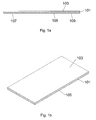
- Figure 1a is a cross sectional view of silicon having an oxide layer.
- Figure 1b is a perspective view of silicon having an oxide layer.
- a substrate 101 such as a silicon substrate, for example, a double side polished (DSP) wafer, is oxidized on both sides through a process such as thermal oxidation to create a first oxide layer 103 and a second oxide layer 105.
- the thickness of the oxide layer may vary, but may be in the range of 0.1 to 10 microns.
- alignment features 107 and 109 are created through a process such as photolithography.
- the alignment features 107 and 109 are areas where the oxide layer is removed entirely or in part.
- the flowchart of Figure 17 illustrates this as step 001, create oxide layer.
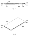
- FIG. 2a is a cross sectional view of the addition of a piezoelectric stack
- Figure 2b is a perspective view of the addition of a piezoelectric stack.
- a first conductive layer 201 for example, Molybdenum in a thickness of from about 100 nm to about 1,000 nm, is deposited.
- Other conductive materials include, for example, gold, copper, platinum and the like.
- a layer of piezoelectric material 203 is deposited on the first conductive layer 201, for example, Aluminum Nitride in a thickness of from about 10 nm to about 500 nm.
- piezoelectric materials include, for example, barium titanate, lead titanate, gallium orthophosphate, bismuth ferrite, sodium potassium niobate, sodium niobate, polyvinylidene fluoride, and the like.
- a second conductive layer 205 On top of the piezoelectric 203 is deposited a second conductive layer 205, for example, Molybdenum in a thickness of from about 100 nm to about 1,000 nm.
- Other conductive materials include, for example, gold, copper, platinum, and the like.
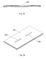
- the first electrode is patterned in step 003.
- Figure 3a is a cross sectional view of the addition of a first electrode pattern.
- Figure 3b is a perspective view of the addition of a first electrode pattern.
- the selective removal 301 of the second conductive layer 205 forms the first electrode pattern.
- Visible in Figure 3b is the first cantilever form half 303 and the second cantilever form half 305.
- the first electrode may be patterned by way of selective material removal, for example by way of selectively etching the second conductive layer 205 with a reactive ion etch such as SF 6 or CF 4 after masking.
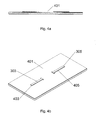
- Step 004 in Figure 17 involves the pattern of piezo material.
- Figure 4a is a cross sectional view of the addition of a piezoelectric pattern.
- Figure 4b is a perspective view of the addition of a piezoelectric pattern.
- a selective removal 401 of the piezoelectric material 203 such as an_etch using KOH with aluminum nitride as the piezoelectric material results in a first cantilever form half 403 and a second cantilever form half 405, as shown in Figure 4b .
- the conductive layer is used as an etch mask to provide a first cantilever form half and a second cantilever form half.
- step 004 the second electrode is patterned from the first conductive layer 201 (depicted in Figure 2 ), as shown in step 005 of Figure 17 .
- Figure 5a is a cross sectional view of the addition of a second electrode pattern.
- Figure 5b is a perspective view of the addition of a second electrode pattern.
- the selective removal 501 of the first conductive layer 201 (depicted in Figure 2 ) forms the second electrode pattern, and as can be seen in Figure 5b , the first cantilever form half 503 and the second cantilever form half 505 are patterned.
- the second electrode may be patterned by way of selective material removal, for example by way of selectively etching the first conductive layer 201 with a reactive ion etch such as SF 6 or CF 4 after masking.
- a reactive ion etch such as SF 6 or CF 4 after masking.
- the first cantilever form half 503 and the second cantilever form half 505 have slightly different geometries at one end to provide a base for bondpads that will provide a current path from the piezoelectric material to electronic packaging with ohmic contacts, such as pins, by way of a technique such as wire bonding or the like.
- Step 006 of Figure 17 is the deposition of bondpads.
- Figure 6a is a cross sectional view of the addition of bond pads.
- Figure 6b is a perspective view of the addition of bond pads.
- the bond pads may be, in one embodiment of the present invention, aluminum that is evaporated and deposited in a rectangular pattern on the electrode material.
- an oxide layer is deposited across the entire work piece.
- An example of such blanket deposition is that of Plasma Enhanced Chemical Vapor Deposition (PECVD) oxide.
- PECVD Plasma Enhanced Chemical Vapor Deposition
- the contact layer which is actually the precursor to electrical contacts to be formed, will be etched such that conductive material may be selectively deposited.
- Figure 7a is a cross sectional view of the addition of a contact layer.
- Figure 7b is a perspective view of the addition of a contact layer.
- a suitable etch would be a reactive ion etch such as CHF 3 /O 2 .
- the patterned contact layer 701 is shown along with the first cantilever form half 703 and the second cantilever form half 705 in Figure 7b . Forms for a proof mass can also be seen at the end of each cantilever half.
- a seed layer is deposited, as noted in step 008 of Figure 17 .
- the seed layer is a layer of conductive material that provides the foundation for a later plating step, allowing the plated core to properly bond to its intended surface.
- the seed layer is gold that is evaporated and blanket deposited.
- Figure 8a is a cross sectional view of the addition of a seed layer.
- Figure 8b is a perspective view of the addition of a seed layer. In figures 8a and 8b , the seed layer 801 can be seen.
- FIG. 9a is a cross sectional view of the addition of a plate layer.
- Figure 9b is a perspective view of the addition of a plate layer.
- the plate layer is substantially thicker than the seed layer, and may be in the range of 1-10 microns per side.
- the plate layer comprises what will become the core of the cantilever as well as part of any associated proof mass, should a proof mass be patterned. It is the plate layer of the first cantilever form half that will be bonded to the plate layer of the second cantilever half to form the cantilever.
- Plate refers generically to any process that can be used to form each core half.
- the core can be conductive or nonconductive and can be fabricated using a variety of methods including, but not limited to, electroplating, physical deposition such as sputter deposition and evaporation, chemical deposition, and the like.
- Some embodiments of the present invention create a core as a single layer as opposed to a seed and plate process.
- the work piece has seed layer in unwanted areas, such as areas outside the core and proof mass.
- the seed layer is removed. Removal techniques include deplating or Iodine Potassium Iodide (IKI) etch, for example.
- Figure 10a is a cross sectional view showing the removal of the seed layer.
- Figure 10b is a perspective view showing the removal of the seed layer. The seed layer is shown removed as 1001 in Figures 10a and 10b .
- a similar thickness of plate may be removed. Since there is an unexposed seed layer beneath the plate that is immune to removal, the thickness of the plate after seed removal is the same as the thickness of the plate itself prior to seed removal.
- the two book halves of the energy harvester of the present invention can be clearly seen in Figure 10b , and have been built up to the point where they are ready to be joined together to make a completed cantilever.
- two wafers containing a plurality of devices are joined together such that the book halves are aligned and where a first cantilever form half on the first wafer aligns with the second cantilever form half on the second wafer.
- the book halves are each cut from the same wafer, aligned, and then joined.
- a first wafer contains all first cantilever form halves and a second wafer contains all second cantilever form halves.
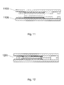
- Figure 11 is a cross sectional view showing wafer alignment where the first cantilever form half 1103 and the second cantilever form half 1105 are aligned and ready for bonding.
- FIG. 12 is a cross sectional view showing wafer bonding 1201.
- the exposed plate sections of each half are bonded together in a process such as, for example, thermo-compression bonding.
- the exposed plate sections once bonded become the cantilever core and part of any associated proof mass.
- the second electrode of the first cantilever form half becomes the top electrode of the bimorph structure
- the second electrode of the second cantilever half form becomes the bottom electrode of the bimorph structure
- the first electrodes of each cantilever form half, along with the core become the common electrode of the bimorph structure.
- feedthroughs provide a conductive path for electrical signals to travel from the top electrode down to leads and bondpads on the bottom level.
- step 013 of Figure 17 the proof mass is patterned.
- Figure 13 is a cross sectional view showing the proof mass being patterned.
- a proof mass etch 1301 is performed to define the proof mass and surrounding support structures.
- FIG 14 is a cross sectional view showing singulation and release.
- Each device is singulated by cutting (dicing) or breaking the bonded silicon wafers.
- the sacrificial silicon dioxide supporting the cantilever and proof mass is then removed using a selective etch such as CHF 3 /O 2 RIE or HF (hydrogen fluoride) vapor, and the cantilever is now free to move.
- the order of the singulation and sacrificial release may be reversed depending upon whether the sacrificial release is performed on the wafer or on individual chips.
- step 015 of Figure 17 illustrates a cap/package step where the energy harvester that has been fabricated and is free to move receives optional cap wafers or similar protective packaging.
- the protective packaging provides a controlled environment for the energy harvester to protect it from damage as well as to affect its performance.
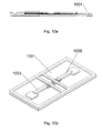
- Figure 15 is a cross sectional view of the device capped.
- a first cap 1507 and a second cap 1509 are placed on each side of the cantilever 1501.
- the released proof mass 1503 can be seen with the integral core contained therewith.
- a void 1505 is present.
- This void may be left as ambient air, or may, in some embodiments of the present invention, be filled with a gas such as an inert gas, or even a fluid. Gas may be provided at a reduced pressure, or even a vacuum.
- the capping process may also be performed at the chip level or at the wafer level prior to singulation. Variation in gas parameters such as pressure, mix, and the like will affect device performance such as damping which in turn affects bandwidth, power amplitude, and the like. These variations can be used to control, for example, device performance for an intended application.
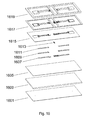
- Figure 16 is an exploded view showing the layers of the device that correspond to the previous step by step description of the energy harvesting device.
- Figure 16 shows the layers before the two halves of the device are aligned, bonded, and cut.
- 1601 is a first oxide.
- 1603 is a substrate such as, for example, silicon.
- 1605 is a second oxide.
- 1607 is a first conductive layer.
- 1609 is a piezoelectric material.
- 1611 is a second conductive layer.
- 1613 are bond pads.
- 1615 is a contact layer.
- 1617 is a seed layer, and 1619 is a plate layer.
- Figure 17 depicts a flowchart showing processing steps, and has previously been described.
- Figure 18 is a perspective view of the pre-bonded assembly 1801 prior to alignment, bond, and cut.
- Figure 19 is a perspective view of the aligned, bonded, and cut energy harvesting device 1901 with the cantilever free to move.
- the energy harvesting device 1901
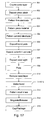
- Figure 20 depicts a chip with exemplary cantilevers of the present invention.
- the chip 2000 contains, for example, a rectangular cantilever 2001, a rectangular cantilever with proof mass 2003, a trapezoidal cantilever with proof mass 2005, a trapezoidal cantilever 2007, and other geometries made with the process herein described are all within the scope of the present invention and the various embodiments described and envisioned herein.
Description
- The present invention relates generally to energy scavengers and energy harvesters which convert ambient forms of energy into electricity, and more particularly to vibrational energy harvesters that convert environmental mechanical vibrational energy to electrical energy utilizing piezoelectric type materials. Such apparatusses are inter alia known from the
US 2005/280334 ,WO 2008/116173 andUS 2007/114890 . - One of the most familiar types of energy harvester is the solar cell. Additionally, there are energy harvesters that convert thermal gradients, wind power, water power, and the like into electric power. To take advantage of these types of energy harvesters, environmental contact such as exposure to light, thermal gradients, wind, water, and the like is required. These types of energy harvesters are not commonly found in enclosed environmental spaces such as HVAC systems or walls, embedded in machinery or tissue, or other applications that do not have access to external environmental energy sources.
- Alternatively, vibrational type energy harvesters (VEHs) are able to take advantage of environmental vibrations created by appliances, HVAC (Heating Ventilating and Air-Conditioning) systems, equipment, motors, human movement, and the like, to produce electrical power or electricity in open as well as enclosed environmental spaces. These environmental vibrational frequencies are typically found in the 1-1000 Hz range. In general, a VEH comprises a proof mass on a spring. The spring is typically a cantilever beam. The mass / spring combination has a resonant frequency and, although it can respond to a spectrum of vibrational frequencies, it responds most strongly to ambient vibrations around that resonant frequency. This resonant motion can be converted to electricity using techniques such as electromagnetic pick-up or piezoelectric generation.
- Energy harvesters are well known in the art for use in a variety of applications. However, due to the limitations described herein, they are not well known for wireless applications. They have been suggested for wireless sensor applications to provide the electrical energy to power a sensor and/or charge an associated battery. Wireless sensors measure environmental variables and transmit the measured data back to a receiver without any cabling or wires. Typically, the data is transmitted using radio frequency signals and the power for the sensor is provided by a battery, capacitor, or similar energy storage device. Wireless sensors have many potential applications because they can be used where it is difficult to get wires or as after-market system upgrades requiring no additional cabling. Some of the many applications that have been identified that could benefit from wireless sensors include:
- Monitoring of infrastructure integrity, such as buildings and bridges,
- Air quality monitoring in HVAC (heating, ventilation, and air conditioning) systems,
- Monitoring industrial processes, such as chemical or food production,
- Equipment health monitoring,
- Medical implants or mobile personal health monitoring,
- Automotive sensors, such as tire pressure monitors, and
- Defense and security applications such as chemical and biological monitoring of buildings and public spaces.
- These applications have not developed as quickly as predicted, in part, because of the difficulty of providing power to the sensors. Although batteries can be used, they have a limited life and must be replaced periodically. Since remote sensors are typically placed in inaccessible places (because of the difficulty of running wiring), battery changing can be difficult or impossible. There is additionally a cost for using batteries which includes labor, the recurring cost of the battery, and disposal, with its attendant environmental concerns.
- One solution to this wireless sensor power problem is to provide power using energy scavengers or energy harvesters which can convert ambient forms of energy into electricity for use by the sensor or for charging the battery. Microfabricated MEMS VEH devices may provide such a solution.
- Microfabricated VEH Devices (µVEHs), however, have their own set of problems. Typically, a piezoelectric MEMS µVEH consists of a cantilever beam element capped with a piezoelectric film and terminated with a proof mass. When the device vibrates, the mass stresses the cantilever beam, including the piezoelectric film. The stress in the piezoelectric film generates charge and a voltage difference is created across the capacitor formed by the piezoelectric between the top and bottom surfaces.
- The resonant frequency (f) of a spring / mass combination is represented by the equation f= (1/2π)(k/M)½, where k is the spring constant and M is the proof mass. Because of their small size (i.e. short springs and small masses), µVEHs typically have high resonant frequencies (>500 Hz). In order to achieve the desired low resonant frequency configuration and sensitivity, the cantilever beam (spring) must be long (a few mm), thin, and compliant, and the mass must be large (a few milligrams). For MEMS µVEHs, this is difficult. MEMS fabrication is based on thin film processing techniques developed by the semiconductor industry. Conducting, insulating, semiconductor, and piezoelectric films are deposited using sputtering, vacuum evaporation, or chemical vapor deposition and are typically only 1-3 microns thick (or less). A 5 micron thick film is a very thick film deposition for a microfabrication process. It is relatively difficult to construct large structures with such thin film fabrication techniques.
- Additionally piezoelectric µVEHs produce voltages of only a few hundredths of a volt and power levels of only a few µW or less. One of the primary reasons for such low outputs is the limited stress that can be applied to the piezoelectric element. It is known in the art that the stress in a bending cantilever beam element is proportional to the distance of the element from the neutral axis of the cantilever. The neutral axis is defined as the line where the stress is zero. When the cantilever bends downward, the stress above the neutral axis is tensile. Below the neutral axis, it is compressive. When it bends upward, the stresses reverse. If the neutral axis falls inside the piezoelectric material, the charge generated above the neutral axis is canceled by charge of the opposite polarity generated below. In the design of an energy harvester, then, it is desirable to keep the neutral axis outside the piezoelectric element.
- The easiest way to get the entire piezoelectric film away from the neutral axis is to deposit it on a base. This is commonly achieved by placing the thin piezoelectric film on a thicker silicon (Si) or silicon dioxide mechanical cantilever. This single element, or monomorph, architecture can be fabricated several ways. One way is to deposit the mechanical base layer on a standard Si wafer prior to deposition of the piezoelectric and electrode films. This base layer must be relatively thick (in microelectronics terms), for example, 3-5 microns thick. Even so, the neutral axis will be just inside or just below the piezoelectric. A second approach is to use a silicon-on-insulator (SOI) wafer that has a single crystal silicon layer a few microns thick atop a buried oxide layer which again is atop a thick handle.
- In both cases, the bulk of the silicon wafer is etched off the back under the piezoelectric, leaving the piezoelectric film and the support layer (either oxide or silicon) freely suspended. Because the neutral axis is so close to the piezoelectric element, only low stresses are produced, so these MEMS µVEHs tend to generate only a few hundredths to tenths of a volt per "g" of acceleration, where "g" is the acceleration due to gravity.
- A second limitation of the MEMS monomorph architecture is that the mechanical energy that drives the cantilever must be shared between bending the support cantilever and bending the piezoelectric element. The energy that is required to bend the support does not go into straining the piezoelectric, thereby limiting the amount of voltage that can be developed.
- One approach that has been employed to compensate for the low stress and enhance the output voltage is to connect multiple cantilevers in series. The difficulty with this approach is that in order to respond identically to input acceleration, the cantilevers and proof masses must be identical. Otherwise, they will have different resonant frequencies or phases and interfere with one another. Microfabrication process variations have to be well controlled. Additionally, valuable chip space is lost since it must be used for redundant cantilevers to boost output at a single frequency. This chip space could more advantageously be used for cantilevers with different resonant frequencies to broaden the band of harvested frequencies.
- Another approach that has been taken to enhance the generated voltage is to fabricate a piezoelectric bimorph on the support cantilever. This, however, has its own difficulties. Fabrication of a MEMS bimorph requires several additional thin film depositions to prevent shorting of the layers together when bondpad metallization is deposited. These additional thin film depositions include the extra piezoelectric element, electrode and additional insulation layers. Several additional photomasks are also required to permit etching of the first electrode and piezoelectric element in order to gain access to the center electrode and to open up electrical contacts in the insulating layer. One thin film piezoelectric, PZT (Lead Zirconate Titanate), is commonly used because of its high piezoelectric constant. However, PZT is very difficult to etch. Aluminum nitride (AlN) has been commonly used instead because it is very compatible with semiconductor processes, and can be etched. However, finding etches that are selective between AlN and its common electrode material molybdenum (Mo) is also challenging. Another challenge is that precision is required when building the bimorph to get the numerous film thicknesses correct in order to place the neutral axis correctly.
- An issue all the aforementioned MEMS approaches have in common is film stress gradient control. Each of the depositions are typically performed at different temperatures, such that as the film stacks are built up, differential thermal expansion of the substrate and films build up stresses in the stack. These are typically very tensile stresses. When the final release of the cantilever takes place, the stresses can cause the cantilevers to curl up, sometimes well over 360°. This built in stress can be mitigated by adding a compressive overlayer of oxide. Unfortunately, however, the thickness of this compensating layer has to be fine tuned to balance out the stack stress. This can be accomplished, but balancing acts are hard to maintain, as processes and materials possess variability.
- It is therefore an object of the present invention to provide an energy harvester with a cantilever structure not prone to physical defects. It is another object of the present invention to provide an energy harvester with improved power output. It is yet another object of the present invention to provide an energy harvester with improved efficiencies and greater frequency range. It is another object of the present invention to provide an energy harvester with improved energy transfer. These and other objects of the present invention are not to be considered comprehensive or exhaustive, but rather, exemplary of objects that may be ascertained after reading this specification with the accompanying drawings and claims.
- In accordance with the present invention, there is provided a vibrational energy harvesting device comprising a cantilever having a first end, a second end and a core having a first planar surface and a second planar surface, the core being fabricated as two plate layers and bonded together; a first piezoelectric stack having a piezoelectric material placed between a first conductive layer and a second conductive layer and attached to the first planar surface of said core; a second piezoelectric stack having a piezoelectric material placed between a first conductive layer and a second conductive layer and attached to the second planar surface of said core; and a casing wherein the first end of the cantilever is joined to the casing and the second end is free to move.
- The foregoing paragraph has been provided by way of introduction, and is not intended to limit the scope of the following claims.
- The invention will be described by reference to the following drawings, in which like numerals refer to like elements, and in which:
-
Figure 1a is a cross sectional view of silicon having an oxide layer; -
Figure 1b is a perspective view of silicon having an oxide layer; -
Figure 2a is a cross sectional view of the addition of a piezoelectric stack; -
Figure 2b is a perspective view of the addition of a piezoelectric stack; -
Figure 3a is a cross sectional view of the addition of a first electrode pattern; -
Figure 3b is a perspective view of the addition of a first electrode pattern; -
Figure 4a is a cross sectional view of the addition of a piezoelectric pattern; -
Figure 4b is a perspective view of the addition of a piezoelectric pattern; -
Figure 5a is a cross sectional view of the addition of a second electrode pattern; -
Figure 5b is a perspective view of the addition of a second electrode pattern; -
Figure 6a is a cross sectional view of the addition of bond pads; -
Figure 6b is a perspective view of the addition of bond pads; -
Figure 7a is a cross sectional view of the addition of a contact layer; -
Figure 7b is a perspective view of the addition of a contact layer; -
Figure 8a is a cross sectional view of the addition of a seed layer; -
Figure 8b is a perspective view of the addition of a seed layer; -
Figure 9a is a cross sectional view of the addition of a plate layer; -
Figure 9b is a perspective view of the addition of a plate layer; -
Figure 10a is a cross sectional view showing the removal of the seed layer; -
Figure 10b is a perspective view showing the removal of the seed layer; -
Figure 11 is a cross sectional view showing wafer alignment; -
Figure 12 is a cross sectional view showing wafer bonding; -
Figure 13 is a cross sectional view showing the proof mass being patterned; -
Figure 14 is a cross sectional view showing singulation and release; -
Figure 15 is a cross sectional view of the device capped; -
Figure 16 is an exploded view showing the layers of the device; -
Figure 17 is a flowchart showing processing steps; -
Figure 18 is a perspective view of the device prior to bonding; -
Figure 19 is a perspective view of the bonded device; and -
Figure 20 depicts a chip with exemplary cantilevers of the present invention; - The present invention will be described in connection with a preferred embodiment, however, it will be understood that there is no intent to limit the invention to the embodiment described.
- For a general understanding of the present invention and the various embodiments described or envisioned herein, reference is made to the drawings. In the drawings, like reference numerals have been used throughout to designate identical elements.
- MEMS: Micro-Electro-Mechanical Systems. MEMS are integrated circuits (ICs) manufactured using processes and equipment similar to that used in the microelectronics industry. MEMS ICs include mechanical, fluidic, or optical elements in addition to electrical circuits. MEMS ICs are used for applications such as miniature sensors and transducers.
- Piezoelectric: A material property for which the application of a force or stress to a piezoelectric sensitive material results in the development of a charge in the material which in turn generates an electric field in the material. The piezoelectric property is a tensor property. The application of a stress along one dimension can result in an electric field being generated along another dimension.
- Vibrational energy harvester: A device which uses ambient environmental vibrational energy (e.g. equipment or motor vibrations, footsteps) to generate electricity. This electricity can be used in a variety of applications such as to replace or recharge batteries for applications that do not have access to line power.
- Bimorph: A bimorph is a piezoelectric device consisting of two piezoelectric elements attached to each other or to an intermediate support to form a bending element. The piezoelectric elements are positioned so that they are parallel to each other and located on either side of the neutral axis formed by the combination.
- Elastic element: An elastic element is a mechanical element which obeys Hooke's Law: F = kΔx. That is, a displacement Δx from equilibrium of the mechanical element produces a restoring force F that is proportional to the displacement. The constant of proportionality k is commonly referred to as the spring constant. The most common elastic element is a mass on a spring. For the energy harvester of the present invention the elastic element is a bending element which is stationary at one end and for which the displacement is the deviation from equilibrium of the unsupported end.
- Thin film: Thin films are the key components of all microelectronics and MEMS processes. A thin film is a thin layer of a material (e.g. metal, insulator, or semiconductor) which is deposited on a substrate (typically a silicon wafer, although other wafer substrates such as glass, ceramic, and gallium arsenide can be used) using one of several methods common in the semiconductor / MEMS industry. These include PVD (physical vapor deposition - sputtering and vacuum evaporation), diffusion (thermal oxide growth), CVD (chemical vapor deposition including both Low Pressure CVD (LPCVD) and Plasma Enhanced CVD (PECVD), Molecular Beam Epitaxy (MBE), and Atomic Layer Deposition (ALD). These films range from monolayers only a few Angstroms thick to typically less than 10 microns thick.
- Electrically insulating film or layer: An electrical insulator is a material which does not conduct electricity. In microelectronics and MEMS these films are typically silicon dioxide (SiO2) or silicon nitride (Si3N4) or non-stoichiometric films containing silicon and oxygen or nitride, or metal oxides.
- Etch mask: In order to build microelectronic or MEMS devices it is necessary to etch patterns into the thin films. This is typically accomplished by coating the layer with a photoimageable material (photoresist) into which the desired pattern is exposed with a photomask and developed, similar to photographic film. The pattern can then be etched into the thin film with a wet chemical or dry plasma etch, after which the photoresist is removed. Sometimes the pattern etched into the thin film can be used as a further mask for etching underlying films.
- Etch stop: MEMS fabrication processes often rely on the selectivity to different materials of the etches used. The hard etch mask described above is an example of that. The hard mask is resistant to the chemistry used to etch the layers below it. This selectivity can also be used to determine how deep an etch can go. An etch stop is a buried layer of material that is resistant to the etch chemistry. Thus when a material is being etched, the etch will continue until it reaches the resistant material below (the etch stop), and etch no further.
- Sacrificial layer: Sacrificial layers are key elements in fabricating MEMS. A sacrificial layer is a thin film that is deposited and upon which a subsequent layer or layers of thin films are deposited and patterned to form the MEMS mechanical structure. The final step of the MEMS process is to selectively etch out the sacrificial layer, leaving the MEMS structure free to move.
- A novel High Efficiency MEMS Micro-Vibrational Energy Harvester (µVEH) having a thick beam bimorph architecture is described. The architecture of the present invention places energy harvesting elements "face-to-face" to form a bimorph with its neutral axis in a central thick core layer.
- There are many advantages of this configuration. First, this approach enables a MEMS architecture with long cantilever springs and a large proof mass, thereby enabling response to low frequencies. Second, the piezoelectric elements can be placed arbitrarily far from the neutral axis, thus increasing the stress on (and voltage output from) the piezoelectric element. When stressed, each element in its entirety is in either compression or tension, thereby increasing efficiency. Third, a cantilever support layer is no longer necessary, and can be partially or completely eliminated, allowing more of the input mechanical force to be applied to the piezoelectric elements. Fourth, the bimorph is created by bonding wafers face-to-face, eliminating the need for complex multi-film, multi-process bimorph structures. Fifth, since the piezoelectric elements are bonded face-to-face, any differential film-stresses built into the film stacks will be self-compensated, since the films will push against each other. A single bimorph using this architecture will produce sufficient voltage and power to eliminate the need for multiple connected harvesters working at the same resonant frequency.
- The present invention is a MEMS piezoelectric vibrational energy harvester having a "thick beam bimorph" architecture. The vibrational energy harvester comprises a free-floating mass, referred to as a "proof mass", which is attached to one end of one or more elastic elements, each of which is attached at the opposing end to a stationary support. The elastic element includes two piezoelectric elements, each element of which contains at least one piezoelectric film with a first electrode and a second electrode, and both elements separated by a spacer or spacers forming a thick beam region through and parallel to which the neutral axis of the spring passes. A cantilever is an example of an elastic element.
- This "thick beam" architecture ensures that each piezoelectric element is, in its entirety, in tension or compression, thus increasing the efficiency of the energy harvester. Each piezoelectric element can be displaced by the spacers arbitrarily far from the neutral axis, thus increasing the stress in the piezoelectric elements for a given cantilever beam deflection and thereby increasing the output power for a given elastic element deflection. The neutral axis defines the plane above which the stress, and hence the charge and electric field generated, has one polarity and below which it has the opposite polarity. If the neutral axis lies within a piezoelectric element, the electric field below the axis will cancel a portion of the field above the axis, leading to inefficient voltage generation. For large energy harvesters, this is avoided by using a bimorph architecture in which two piezoelectric elements are stacked, placing the neutral axis between them. For MEMS energy harvesters, which use thin piezoelectric films for the piezoelectric elements, this is avoided by building the piezoelectric film on top of a thicker elastic substrate. MEMS bimorphs can be fabricated on the elastic substrate, but film thickness control becomes critical if the neutral axis is to lie between these thin films.
- The amount of stress developed in a piezoelectric material is proportional to its distance from the neutral axis. Because the films used to fabricate MEMS vibrational energy harvesters (VEHs) are so thin, it is difficult to get the piezoelectric element far from the neutral axis. The thick beam bimorph architecture uses spacers that can be made arbitrarily thick. Thus, the piezoelectric elements can be placed farther from the neutral axis than is possible for most MEMS designs, thereby increasing the output power and voltage for a given cantilever deflection.
- One way some MEMS VEHs get the piezoelectric film far from the neutral axis is to deposit the film on a wafer and then etch away most of the wafer under the film leaving the piezoelectric film supported by a thick layer of silicon which acts as an elastic support element. This elastic element can then be tens of microns thick, successfully lifting the piezoelectric element away from the neutral axis. However, it is very difficult, if not impossible, to build a bimorph by fabricating a second piezoelectric element on the backside of this thick silicon support element.
- The thick beam bimorph architecture of the present invention eliminates these issues by providing a thick spacer which can be plated or otherwise deposited to any desired thickness.
- To fully describe how to make and use the present invention and various embodiments and variants thereof, a series of drawings is presented.
Figures 1-15 describe each of the processing steps involved in fabricating the present invention. InFigures 1-10 , each figure is accompanied by an "a" view and a "b" view. The "a" view is a cross sectional view of the layers, material and structure of the present invention. The "b" view is a perspective view of the present invention at the point of processing depicted in the "a" view.Figures 11-15 depict the final processing steps of the novel energy harvester of the present invention. It should be observed through the drawings that many of the improvements to energy harvesting come about through the novel aspects of process and structure. For example, the energy harvester of the present invention is built using two "book halves" that are bonded together to form an improved cantilever structure.Figure 18 clearly shows the two "book halves" prior to bonding, andFigure 19 clearly shows the two "book halves" after bonding and before capping and final packaging and assembly.Figure 16 provides an exploded view of the layers and materials of the energy harvester of the present invention. The processing steps taken to fabricate the novel energy harvester are provided inFigure 17 , the callout numbers corresponding to previous figure numbers to thoroughly and adequately describe how to make the present invention. Variations on each of these steps can be taken to better suit constraints such as environment, cost, production equipment, application, and the like. Lastly,Figure 20 provides several exemplary geometries of the energy harvester of the present invention contained on a chip. To use the energy harvester of the present invention, a suitable package such as, for example, a ceramic or plastic structure, contains the energy harvester of the present invention. Further, in some embodiments of the present invention, the energy harvester may be contained within or upon a chipset. A chipset is a structure that may contain the energy harvester alone or with other devices such as microelectronic devices, other micro electro mechanical machines, energy storage devices, sensors, and the like. The energy harvester is connected either directly to a device requiring electrical power or an electrical energy storage device such as a battery or an ultracapacitor with the appropriate power rectification circuitry for converting oscillatory current electric power to direct current electric power. Such power rectification circuitry is known to those skilled in the art, and may include wave rectification using diodes or similar semiconductor devices. The power rectification circuitry may also include filters to remove unwanted frequencies or harmonics, transient suppressors, and the like. The energy harvester with accompanying electronics is then placed in or upon, or otherwise mechanically coupled to, an environmental element that is generating vibrational energy to be harvested. Such environmental elements could be, for example, a bridge, a roadway, machinery, transportation equipment, electrical equipment, oscillatory structures or devices, and the like. The energy harvester of the present invention may be adapted to various resonant frequencies to efficiently harvest the vibrational energy of its host by way of modifying the length of the cantilever, the geometry of the cantilever, the proof mass of the cantilever, the space surrounding the cantilever, the cavity or structure of the energy harvester, the addition of elements to the energy harvester such as frequency tuning or phase shift structures, and the like. - To begin construction of the energy harvester of the present invention, a wafer or similar substrate, such as a silicon wafer, is oxidized through a process such as thermal oxidation. By way of example and not limitation,
Figure 1a is a cross sectional view of silicon having an oxide layer.Figure 1b is a perspective view of silicon having an oxide layer. Asubstrate 101 such as a silicon substrate, for example, a double side polished (DSP) wafer, is oxidized on both sides through a process such as thermal oxidation to create afirst oxide layer 103 and asecond oxide layer 105. The thickness of the oxide layer may vary, but may be in the range of 0.1 to 10 microns. To facilitate fabrication, alignment features 107 and 109 are created through a process such as photolithography. The alignment features 107 and 109 are areas where the oxide layer is removed entirely or in part. The flowchart ofFigure 17 illustrates this asstep 001, create oxide layer. - The next processing step, described in
Figure 17 asstep 002 deposit piezo stack, is depicted by way ofFigures 2a and 2b whereFigure 2a is a cross sectional view of the addition of a piezoelectric stack andFigure 2b is a perspective view of the addition of a piezoelectric stack. A first conductive layer 201, for example, Molybdenum in a thickness of from about 100 nm to about 1,000 nm, is deposited. Other conductive materials include, for example, gold, copper, platinum and the like. Then a layer ofpiezoelectric material 203 is deposited on the first conductive layer 201, for example, Aluminum Nitride in a thickness of from about 10 nm to about 500 nm. Other piezoelectric materials include, for example, barium titanate, lead titanate, gallium orthophosphate, bismuth ferrite, sodium potassium niobate, sodium niobate, polyvinylidene fluoride, and the like. On top of the piezoelectric 203 is deposited a secondconductive layer 205, for example, Molybdenum in a thickness of from about 100 nm to about 1,000 nm. Other conductive materials include, for example, gold, copper, platinum, and the like. - As depicted in
Figure 17 , the first electrode is patterned instep 003.Figure 3a is a cross sectional view of the addition of a first electrode pattern.Figure 3b is a perspective view of the addition of a first electrode pattern. Theselective removal 301 of the second conductive layer 205 (depicted inFigure 2 ) forms the first electrode pattern. Visible inFigure 3b is the firstcantilever form half 303 and the secondcantilever form half 305. The first electrode may be patterned by way of selective material removal, for example by way of selectively etching the secondconductive layer 205 with a reactive ion etch such as SF6 or CF4 after masking. - Step 004 in
Figure 17 involves the pattern of piezo material.Figure 4a is a cross sectional view of the addition of a piezoelectric pattern.Figure 4b is a perspective view of the addition of a piezoelectric pattern. Aselective removal 401 of the piezoelectric material 203 (depicted inFigure 2 ) such as an_etch using KOH with aluminum nitride as the piezoelectric material results in a firstcantilever form half 403 and a secondcantilever form half 405, as shown inFigure 4b . The conductive layer is used as an etch mask to provide a first cantilever form half and a second cantilever form half. - Once
step 004 is completed, the second electrode is patterned from the first conductive layer 201 (depicted inFigure 2 ), as shown instep 005 ofFigure 17 .Figure 5a is a cross sectional view of the addition of a second electrode pattern.Figure 5b is a perspective view of the addition of a second electrode pattern. Theselective removal 501 of the first conductive layer 201 (depicted inFigure 2 ) forms the second electrode pattern, and as can be seen inFigure 5b , the firstcantilever form half 503 and the secondcantilever form half 505 are patterned. The second electrode may be patterned by way of selective material removal, for example by way of selectively etching the first conductive layer 201 with a reactive ion etch such as SF6 or CF4 after masking. As can be seen inFigure 5b , the firstcantilever form half 503 and the secondcantilever form half 505 have slightly different geometries at one end to provide a base for bondpads that will provide a current path from the piezoelectric material to electronic packaging with ohmic contacts, such as pins, by way of a technique such as wire bonding or the like. - Step 006 of
Figure 17 is the deposition of bondpads.Figure 6a is a cross sectional view of the addition of bond pads.Figure 6b is a perspective view of the addition of bond pads. The bond pads may be, in one embodiment of the present invention, aluminum that is evaporated and deposited in a rectangular pattern on the electrode material. - In
step 007 ofFigure 17 , an oxide layer is deposited across the entire work piece. An example of such blanket deposition is that of Plasma Enhanced Chemical Vapor Deposition (PECVD) oxide. The contact layer, which is actually the precursor to electrical contacts to be formed, will be etched such that conductive material may be selectively deposited.Figure 7a is a cross sectional view of the addition of a contact layer.Figure 7b is a perspective view of the addition of a contact layer. In the case of Plasma Enhanced Chemical Vapor Deposition (PECVD) oxide being used, a suitable etch would be a reactive ion etch such as CHF3/O2. Thepatterned contact layer 701 is shown along with the firstcantilever form half 703 and the secondcantilever form half 705 inFigure 7b . Forms for a proof mass can also be seen at the end of each cantilever half. - Once the contact layer is deposited and suitably patterned, in one embodiment of the present invention a seed layer is deposited, as noted in
step 008 ofFigure 17 . The seed layer is a layer of conductive material that provides the foundation for a later plating step, allowing the plated core to properly bond to its intended surface. In one embodiment of the present invention, the seed layer is gold that is evaporated and blanket deposited.Figure 8a is a cross sectional view of the addition of a seed layer.Figure 8b is a perspective view of the addition of a seed layer. Infigures 8a and 8b , theseed layer 801 can be seen. - Once the seed layer is deposited, plating of a material compatible with the seed layer commences. The plated material covers the seed layer and may be, in one embodiment, gold, and whereas the seed layer may be gold as well. Step 009 of
Figure 17 is the Plate step.Figure 9a is a cross sectional view of the addition of a plate layer.Figure 9b is a perspective view of the addition of a plate layer. The plate layer is substantially thicker than the seed layer, and may be in the range of 1-10 microns per side. The plate layer comprises what will become the core of the cantilever as well as part of any associated proof mass, should a proof mass be patterned. It is the plate layer of the first cantilever form half that will be bonded to the plate layer of the second cantilever half to form the cantilever. - Plate, as used herein, refers generically to any process that can be used to form each core half. In further embodiments of the present invention, the core can be conductive or nonconductive and can be fabricated using a variety of methods including, but not limited to, electroplating, physical deposition such as sputter deposition and evaporation, chemical deposition, and the like. Some embodiments of the present invention create a core as a single layer as opposed to a seed and plate process.
- At this step in processing, the work piece has seed layer in unwanted areas, such as areas outside the core and proof mass. At
step 010 ofFigure 17 , the seed layer is removed. Removal techniques include deplating or Iodine Potassium Iodide (IKI) etch, for example.Figure 10a is a cross sectional view showing the removal of the seed layer.Figure 10b is a perspective view showing the removal of the seed layer. The seed layer is shown removed as 1001 inFigures 10a and 10b . In the removal of the unwanted areas of seed layer, a similar thickness of plate may be removed. Since there is an unexposed seed layer beneath the plate that is immune to removal, the thickness of the plate after seed removal is the same as the thickness of the plate itself prior to seed removal. - At this point in processing, the two book halves of the energy harvester of the present invention can be clearly seen in
Figure 10b , and have been built up to the point where they are ready to be joined together to make a completed cantilever. In one production method, two wafers containing a plurality of devices are joined together such that the book halves are aligned and where a first cantilever form half on the first wafer aligns with the second cantilever form half on the second wafer. In another production method the book halves are each cut from the same wafer, aligned, and then joined. In another production method a first wafer contains all first cantilever form halves and a second wafer contains all second cantilever form halves.Figure 11 is a cross sectional view showing wafer alignment where the firstcantilever form half 1103 and the secondcantilever form half 1105 are aligned and ready for bonding. - In step 011/012 of
Figure 17 , wafer bonding occurs.Figure 12 is a cross sectional view showingwafer bonding 1201. Once alignment of the first cantilever half form and the second cantilever half form takes place as previously described, the exposed plate sections of each half are bonded together in a process such as, for example, thermo-compression bonding. The exposed plate sections once bonded become the cantilever core and part of any associated proof mass. After bonding, the second electrode of the first cantilever form half becomes the top electrode of the bimorph structure, the second electrode of the second cantilever half form becomes the bottom electrode of the bimorph structure, and the first electrodes of each cantilever form half, along with the core, become the common electrode of the bimorph structure. In addition, feedthroughs provide a conductive path for electrical signals to travel from the top electrode down to leads and bondpads on the bottom level. - In
step 013 ofFigure 17 , the proof mass is patterned.Figure 13 is a cross sectional view showing the proof mass being patterned. Aproof mass etch 1301 is performed to define the proof mass and surrounding support structures. - Once the proof mass is patterned, a singulate/
release step 014 is performed, as shown inFigure 17 .Figure 14 is a cross sectional view showing singulation and release. Each device is singulated by cutting (dicing) or breaking the bonded silicon wafers. The sacrificial silicon dioxide supporting the cantilever and proof mass is then removed using a selective etch such as CHF3/O2 RIE or HF (hydrogen fluoride) vapor, and the cantilever is now free to move. The order of the singulation and sacrificial release may be reversed depending upon whether the sacrificial release is performed on the wafer or on individual chips. - Finally, step 015 of
Figure 17 illustrates a cap/package step where the energy harvester that has been fabricated and is free to move receives optional cap wafers or similar protective packaging. The protective packaging provides a controlled environment for the energy harvester to protect it from damage as well as to affect its performance. -
Figure 15 is a cross sectional view of the device capped. Afirst cap 1507 and asecond cap 1509 are placed on each side of thecantilever 1501. The releasedproof mass 1503 can be seen with the integral core contained therewith. When capping the energy harvester instep 015, avoid 1505 is present. This void may be left as ambient air, or may, in some embodiments of the present invention, be filled with a gas such as an inert gas, or even a fluid. Gas may be provided at a reduced pressure, or even a vacuum. The capping process may also be performed at the chip level or at the wafer level prior to singulation. Variation in gas parameters such as pressure, mix, and the like will affect device performance such as damping which in turn affects bandwidth, power amplitude, and the like. These variations can be used to control, for example, device performance for an intended application. -
Figure 16 is an exploded view showing the layers of the device that correspond to the previous step by step description of the energy harvesting device.Figure 16 shows the layers before the two halves of the device are aligned, bonded, and cut. 1601 is a first oxide. 1603 is a substrate such as, for example, silicon. 1605 is a second oxide. 1607 is a first conductive layer. 1609 is a piezoelectric material. 1611 is a second conductive layer. 1613 are bond pads. 1615 is a contact layer. 1617 is a seed layer, and 1619 is a plate layer.Figure 17 depicts a flowchart showing processing steps, and has previously been described.Figure 18 is a perspective view of thepre-bonded assembly 1801 prior to alignment, bond, and cut.Figure 19 is a perspective view of the aligned, bonded, and cutenergy harvesting device 1901 with the cantilever free to move. Theenergy harvesting device 1901 has yet to receive end caps, packaging, or related components. - Lastly,
Figure 20 depicts a chip with exemplary cantilevers of the present invention. As previously stated, the geometry and other physical attributes of the cantilever may be modified to suit various intended applications. Thechip 2000 contains, for example, arectangular cantilever 2001, a rectangular cantilever withproof mass 2003, a trapezoidal cantilever withproof mass 2005, atrapezoidal cantilever 2007, and other geometries made with the process herein described are all within the scope of the present invention and the various embodiments described and envisioned herein. - It is, therefore, apparent that there has been provided, in accordance with the various objects of the present invention, a High-efficiency MEMS Micro-Vibrational Energy Harvester and Process for Manufacturing Same.
Claims (15)
- A vibrational energy harvesting device comprising:a cantilever (303;305) having a first end, a second end and a core having a first planar surface and a second planar surface, the core being fabricated as two plate layers and bonded together;a first piezoelectric stack having a piezoelectric material (203) placed between a first conductive layer (205) and a second conductive layer (201) and attached to the first planar surface of said core;a second piezoelectric stack having a piezoelectric material (1609) placed between a first conductive layer (1611) and a second conductive layer (1607) and attached to the second planar surface of said core; anda casing wherein the first end of the cantilever is joined to the casing and the second end is free to move.
- The vibrational energy harvesting device as recited in claim 1, further comprising a proof mass (2003;2005) mechanically coupled to the second end of the cantilever.
- The vibrational energy harvesting device as recited in claim 1 or 2, further comprising an electrical contact operatively coupled to said first piezoelectric stack.
- The vibrational energy harvesting device as recited in any of the claims 1 to 3, further comprising an electrical contact operatively coupled to said second piezoelectric stack.
- The vibrational energy harvesting device as recited in any of the claims 1 to 4, wherein said core is gold.
- The vibrational energy harvesting device as recited in any of the claims 1 to 4, wherein said core is copper.
- The vibrational energy harvesting device as recited in any of the claims 1 to 4, wherein said core is nickel.
- The vibrational energy harvesting device as recited in any of the claims 1 to 7, wherein said piezoelectric material (203) is aluminum nitride.
- The vibrational energy harvesting device as recited in any of the claims 1 to 8, wherein said casing is silicon.
- The vibrational energy harvesting device as recited in any of the claims 1 to 9, further comprising a first cap and a second cap.
- The vibrational energy harvesting device as recited claim 10, further comprising an inert gas contained within the first cap and the second cap.
- The vibrational energy harvesting device as recited in claim 11, further comprising a gas at a pressure less than one atmosphere contained within the first cap and the second cap.
- A method of fabricating the vibrational energy harvesting device of any of the claims 1 to 12, comprising the steps of:creating a first wafer set and a second wafer set by
forming an oxide layer on a substrate;
depositing a first and second piezoelectric stack (201;203;205;1607;1609;1611)on the substrate;
patterning a first electrode;
patterning a piezoelectric material;
patterning a second electrode;
depositing bond pads;
depositing a contact layer;
etching contacts in said contact layer;
patterning a core layer;aligning the plate layer of the first wafer set with the plate layer of the second wafer set;bonding said first wafer set to said second wafer set;patterning a resulting vibrational energy harvesting device; andsingulating and releasing the resulting vibrational energy harvesting device. - The method as recited in claim 13, wherein said core layer is formed by the steps of depositing a seed layer and plating said seed layer.
- The method as recited in claim 13 or 14, further comprising the step of capping the resulting vibrational energy harvesting device.
Applications Claiming Priority (3)
| Application Number | Priority Date | Filing Date | Title |
|---|---|---|---|
| US30835410P | 2010-02-26 | 2010-02-26 | |
| US13/030,182 US8593036B2 (en) | 2010-02-26 | 2011-02-18 | High-efficiency MEMS micro-vibrational energy harvester and process for manufacturing same |
| PCT/US2011/025567 WO2011106266A1 (en) | 2010-02-26 | 2011-02-19 | High-efficiency mems micro-vibrational energy harvester and process for manufacturing same |
Publications (3)
| Publication Number | Publication Date |
|---|---|
| EP2539946A1 EP2539946A1 (en) | 2013-01-02 |
| EP2539946A4 EP2539946A4 (en) | 2014-01-29 |
| EP2539946B1 true EP2539946B1 (en) | 2015-07-01 |
Family
ID=44504895
Family Applications (1)
| Application Number | Title | Priority Date | Filing Date |
|---|---|---|---|
| EP11747905.5A Not-in-force EP2539946B1 (en) | 2010-02-26 | 2011-02-19 | High-efficiency mems micro-vibrational energy harvester and process for manufacturing same |
Country Status (4)
| Country | Link |
|---|---|
| US (1) | US8593036B2 (en) |
| EP (1) | EP2539946B1 (en) |
| CA (1) | CA2788316C (en) |
| WO (1) | WO2011106266A1 (en) |
Families Citing this family (28)
| Publication number | Priority date | Publication date | Assignee | Title |
|---|---|---|---|---|
| US9490658B2 (en) * | 2011-12-09 | 2016-11-08 | Nokia Technologies Oy | Apparatus and a method of manufacturing an apparatus |
| KR101774301B1 (en) | 2011-12-16 | 2017-09-20 | 한국전자통신연구원 | energy harvesting device and manufacturing of the same |
| JP6029854B2 (en) | 2012-05-22 | 2016-11-24 | ミネベア株式会社 | Vibrator and vibration generator |
| US10726231B2 (en) | 2012-11-28 | 2020-07-28 | Invensense, Inc. | Integrated piezoelectric microelectromechanical ultrasound transducer (PMUT) on integrated circuit (IC) for fingerprint sensing |
| US9618405B2 (en) | 2014-08-06 | 2017-04-11 | Invensense, Inc. | Piezoelectric acoustic resonator based sensor |
| US9511994B2 (en) | 2012-11-28 | 2016-12-06 | Invensense, Inc. | Aluminum nitride (AlN) devices with infrared absorption structural layer |
| US9114977B2 (en) * | 2012-11-28 | 2015-08-25 | Invensense, Inc. | MEMS device and process for RF and low resistance applications |
| US10497747B2 (en) | 2012-11-28 | 2019-12-03 | Invensense, Inc. | Integrated piezoelectric microelectromechanical ultrasound transducer (PMUT) on integrated circuit (IC) for fingerprint sensing |
| CN104937170B (en) * | 2013-01-14 | 2017-09-05 | 格林瑞尔公司 | Composite railway sleeper and railroad track |
| US9913321B2 (en) * | 2013-01-25 | 2018-03-06 | Energyield, Llc | Energy harvesting container |
| US9890991B2 (en) | 2013-03-14 | 2018-02-13 | Whirlpool Corporation | Domestic appliance including piezoelectric components |
| FR3006112B1 (en) * | 2013-05-24 | 2016-10-21 | Chambre De Commerce Et D'industrie De Region Paris Ile De France | PROCESS FOR MANUFACTURING A FLEXIBLE PIEZOELECTRIC SENSOR |
| WO2015042700A1 (en) | 2013-09-24 | 2015-04-02 | Motion Engine Inc. | Mems components and method of wafer-level manufacturing thereof |
| ITTO20130652A1 (en) * | 2013-07-31 | 2015-02-01 | Milano Politecnico | PIEZOELECTRIC TRANSDUCER FOR AN ENERGY COLLECTION SYSTEM AND METHOD FOR ENERGY COLLECTION BY MEANS OF A PIEZOELECTRIC TRANSDUCER |
| EP3028007A4 (en) | 2013-08-02 | 2017-07-12 | Motion Engine Inc. | Mems motion sensor and method of manufacturing |
| JP6199122B2 (en) * | 2013-09-03 | 2017-09-20 | 吉村 武 | Vibration generator |
| KR101883209B1 (en) | 2013-12-12 | 2018-08-30 | 퀄컴 인코포레이티드 | Micromechanical ultrasonic transducers and display |
| JP6590812B2 (en) | 2014-01-09 | 2019-10-16 | モーション・エンジン・インコーポレーテッド | Integrated MEMS system |
| US20170030788A1 (en) | 2014-04-10 | 2017-02-02 | Motion Engine Inc. | Mems pressure sensor |
| US11674803B2 (en) | 2014-06-02 | 2023-06-13 | Motion Engine, Inc. | Multi-mass MEMS motion sensor |
| US11287486B2 (en) | 2014-12-09 | 2022-03-29 | Motion Engine, Inc. | 3D MEMS magnetometer and associated methods |
| CA3220839A1 (en) | 2015-01-15 | 2016-07-21 | Motion Engine Inc. | 3d mems device with hermetic cavity |
| US10302455B2 (en) * | 2015-10-09 | 2019-05-28 | Bellutech Llc | Modules, systems, and methods for monitoring environmental conditions |
| US11326937B2 (en) | 2016-05-10 | 2022-05-10 | Cornell University | Energy harvesting apparatus and methods for detecting a vibratory signal |
| US10243136B2 (en) | 2016-08-22 | 2019-03-26 | Masoud Ghanbari | Piezoelectric energy harvesting system from vehicle's tires |
| US10694466B2 (en) | 2017-06-20 | 2020-06-23 | University Of South Carolina | Power optimization for a unit cell metamaterial energy harvester |
| CN110252633A (en) * | 2019-06-03 | 2019-09-20 | 北京建筑大学 | A kind of piezo-stack type high-frequency excitation system |
| EP4292209A2 (en) * | 2021-02-12 | 2023-12-20 | University of Exeter | Energy harvesting arrangement and improvements in and relating to power management |
Family Cites Families (27)
| Publication number | Priority date | Publication date | Assignee | Title |
|---|---|---|---|---|
| US3371234A (en) * | 1965-10-15 | 1968-02-27 | Walter G. Cady | Piezoelectric vibrators and systems embodying the same for converting the mechanical vibration thereof into electric energy |
| US3456134A (en) * | 1967-10-05 | 1969-07-15 | Us Health Education & Welfare | Piezoelectric energy converter for electronic implants |
| CA1165860A (en) * | 1979-12-12 | 1984-04-17 | Susumu Nishigaki | Piezoelectric electro-mechanical bimorph transducer |
| JP3185226B2 (en) * | 1991-01-30 | 2001-07-09 | 株式会社村田製作所 | Driving method of piezoelectric bimorph element and piezoelectric bimorph element |
| EP0616221B1 (en) * | 1993-03-19 | 1998-11-25 | Murata Manufacturing Co., Ltd. | Acceleration sensor |
| US5994821A (en) * | 1996-11-29 | 1999-11-30 | Matsushita Electric Industrial Co., Ltd. | Displacement control actuator |
| JPH1130628A (en) * | 1997-07-11 | 1999-02-02 | Matsushita Electric Ind Co Ltd | Bimorph type piezoelectric element for acceleration sensor and manufacture thereof |
| US6550116B2 (en) * | 1997-07-11 | 2003-04-22 | Matsushita Electric Industrial Co., Ltd. | Method for manufacturing a bimorph piezoelectric device for acceleration sensor |
| US6830944B1 (en) * | 1999-03-18 | 2004-12-14 | Trustees Of Boston University | Piezoelectric bimorphs as microelectromechanical building blocks and constructions made using same |
| DE60044666D1 (en) * | 1999-10-01 | 2010-08-26 | Ngk Insulators Ltd | PIEZOELECTRIC / ELECTROSTRICTIVE COMPONENT AND METHOD FOR THE PRODUCTION THEREOF |
| US6642613B1 (en) * | 2000-05-09 | 2003-11-04 | National Semiconductor Corporation | Techniques for joining an opto-electronic module to a semiconductor package |
| US6407484B1 (en) * | 2000-09-29 | 2002-06-18 | Rockwell Technologies Inc | Piezoelectric energy harvester and method |
| JP4806850B2 (en) * | 2001-01-24 | 2011-11-02 | パナソニック株式会社 | Actuator |
| WO2003028059A1 (en) * | 2001-09-21 | 2003-04-03 | Hrl Laboratories, Llc | Mems switches and methods of making same |
| US6777319B2 (en) * | 2001-12-19 | 2004-08-17 | Formfactor, Inc. | Microelectronic spring contact repair |
| WO2003096444A2 (en) * | 2002-05-13 | 2003-11-20 | University Of Florida | Resonant energy mems array and system including dynamically modifiable power processor |
| US6858970B2 (en) * | 2002-10-21 | 2005-02-22 | The Boeing Company | Multi-frequency piezoelectric energy harvester |
| US6895645B2 (en) * | 2003-02-25 | 2005-05-24 | Palo Alto Research Center Incorporated | Methods to make bimorph MEMS devices |
| FR2866122B1 (en) | 2004-02-06 | 2006-05-19 | Europ De Systemes Optiques Soc | MIRROR BIMORPH. |
| JP4377740B2 (en) * | 2004-04-28 | 2009-12-02 | 株式会社東芝 | Piezoelectric drive type MEMS element and mobile communication device having this piezoelectric drive type MEMS element |
| US7239066B2 (en) * | 2004-06-17 | 2007-07-03 | Par Technologies, Llc | Piezoelectric generators and methods of operating same |
| US7692365B2 (en) * | 2005-11-23 | 2010-04-06 | Microstrain, Inc. | Slotted beam piezoelectric composite |
| US20070125176A1 (en) * | 2005-12-02 | 2007-06-07 | Honeywell International, Inc. | Energy harvesting device and methods |
| US20080074002A1 (en) * | 2006-09-26 | 2008-03-27 | Shashank Priya | Piezoelectric energy harvester |
| US7681290B2 (en) * | 2006-10-20 | 2010-03-23 | The Boeing Company | Piezoelectric bimorph beam manufacturing method |
| JP5337721B2 (en) | 2007-03-21 | 2013-11-06 | ザ・ユニバーシティ・オブ・ヴァーモント・アンド・ステイト・アグリカルチュラル・カレッジ | Piezoelectric vibration energy harvesting system incorporating parametric bending mode energy harvesting |
| US7644490B1 (en) * | 2007-05-25 | 2010-01-12 | National Semiconductor Corporation | Method of forming a microelectromechanical (MEMS) device |
-
2011
- 2011-02-18 US US13/030,182 patent/US8593036B2/en not_active Expired - Fee Related
- 2011-02-19 CA CA2788316A patent/CA2788316C/en active Active
- 2011-02-19 EP EP11747905.5A patent/EP2539946B1/en not_active Not-in-force
- 2011-02-19 WO PCT/US2011/025567 patent/WO2011106266A1/en active Application Filing
Also Published As
| Publication number | Publication date |
|---|---|
| US20110210554A1 (en) | 2011-09-01 |
| US8593036B2 (en) | 2013-11-26 |
| WO2011106266A1 (en) | 2011-09-01 |
| CA2788316C (en) | 2016-08-16 |
| CA2788316A1 (en) | 2011-09-01 |
| EP2539946A1 (en) | 2013-01-02 |
| EP2539946A4 (en) | 2014-01-29 |
Similar Documents
| Publication | Publication Date | Title |
|---|---|---|
| EP2539946B1 (en) | High-efficiency mems micro-vibrational energy harvester and process for manufacturing same | |
| US11581827B2 (en) | Energy harvesting with a micro-electro-mechanical system (MEMS) | |
| US7687977B2 (en) | Micromachined, piezoelectric vibration-induced energy harvesting device and its fabrication | |
| US20130127295A1 (en) | Piezoelectric micro power generator and fabrication method thereof | |
| US20070125176A1 (en) | Energy harvesting device and methods | |
| US8080920B2 (en) | Piezoelectric vibrational energy harvesting systems incorporating parametric bending mode energy harvesting | |
| US7992271B2 (en) | Process of manufacturing a piezoelectric actuator for tunable electronic components on a carrier substrate | |
| US20120025337A1 (en) | Mems transducer device having stress mitigation structure and method of fabricating the same | |
| US20090302716A1 (en) | Piezoelectric device | |
| US7851967B2 (en) | Electrostatic induction generator | |
| US20160322559A1 (en) | Mems-based cantilever energy harvester | |
| US20140077662A1 (en) | Piezoelectric apparatus for harvesting energy for portable electronics and method for manufacturing same | |
| JP5988494B2 (en) | Angular velocity sensor and manufacturing method thereof | |
| US20100259130A1 (en) | Device for energy conversion, in particular a piezoelectric micropower converter | |
| US20120049694A1 (en) | Micromachined Piezoelectric Energy Harvester with Polymer Beam | |
| US20130032906A1 (en) | Ferroelectric device | |
| US9502635B2 (en) | Symmetric dual piezoelectric stack microelectromechanical piezoelectric devices | |
| TWI614206B (en) | Mems device for harvesting sound energy and methods for fabricating same | |
| US20130038175A1 (en) | Vibration power generation device | |
| SG173732A1 (en) | Miniaturized piezoelectric accelerometers | |
| Sood et al. | Piezoelectric micro power generator for energy harvesting | |
| US20240130240A1 (en) | Micro electro mechanical system and manufacturing method thereof | |
| Park | Piezoelectric MEMS Energy Harvesters |
Legal Events
| Date | Code | Title | Description |
|---|---|---|---|
| PUAI | Public reference made under article 153(3) epc to a published international application that has entered the european phase |
Free format text: ORIGINAL CODE: 0009012 |
|
| 17P | Request for examination filed |
Effective date: 20120903 |
|
| AK | Designated contracting states |
Kind code of ref document: A1 Designated state(s): AL AT BE BG CH CY CZ DE DK EE ES FI FR GB GR HR HU IE IS IT LI LT LU LV MC MK MT NL NO PL PT RO RS SE SI SK SM TR |
|
| DAX | Request for extension of the european patent (deleted) | ||
| REG | Reference to a national code |
Ref country code: DE Ref legal event code: R079 Ref document number: 602011017497 Country of ref document: DE Free format text: PREVIOUS MAIN CLASS: H01L0041000000 Ipc: H01L0041113000 |
|
| A4 | Supplementary search report drawn up and despatched |
Effective date: 20140108 |
|
| RIC1 | Information provided on ipc code assigned before grant |
Ipc: H02N 2/18 20060101ALI20131220BHEP Ipc: H01L 41/22 20130101ALI20131220BHEP Ipc: H01L 41/113 20060101AFI20131220BHEP |
|
| GRAP | Despatch of communication of intention to grant a patent |
Free format text: ORIGINAL CODE: EPIDOSNIGR1 |
|
| INTG | Intention to grant announced |
Effective date: 20150120 |
|
| GRAS | Grant fee paid |
Free format text: ORIGINAL CODE: EPIDOSNIGR3 |
|
| GRAA | (expected) grant |
Free format text: ORIGINAL CODE: 0009210 |
|
| AK | Designated contracting states |
Kind code of ref document: B1 Designated state(s): AL AT BE BG CH CY CZ DE DK EE ES FI FR GB GR HR HU IE IS IT LI LT LU LV MC MK MT NL NO PL PT RO RS SE SI SK SM TR |
|
| REG | Reference to a national code |
Ref country code: GB Ref legal event code: FG4D |
|
| REG | Reference to a national code |
Ref country code: AT Ref legal event code: REF Ref document number: 734423 Country of ref document: AT Kind code of ref document: T Effective date: 20150715 Ref country code: CH Ref legal event code: EP |
|
| REG | Reference to a national code |
Ref country code: IE Ref legal event code: FG4D |
|
| REG | Reference to a national code |
Ref country code: DE Ref legal event code: R096 Ref document number: 602011017497 Country of ref document: DE |
|
| REG | Reference to a national code |
Ref country code: AT Ref legal event code: MK05 Ref document number: 734423 Country of ref document: AT Kind code of ref document: T Effective date: 20150701 |
|
| REG | Reference to a national code |
Ref country code: NL Ref legal event code: MP Effective date: 20150701 |
|
| REG | Reference to a national code |
Ref country code: LT Ref legal event code: MG4D |
|
| PG25 | Lapsed in a contracting state [announced via postgrant information from national office to epo] |
Ref country code: LV Free format text: LAPSE BECAUSE OF FAILURE TO SUBMIT A TRANSLATION OF THE DESCRIPTION OR TO PAY THE FEE WITHIN THE PRESCRIBED TIME-LIMIT Effective date: 20150701 Ref country code: GR Free format text: LAPSE BECAUSE OF FAILURE TO SUBMIT A TRANSLATION OF THE DESCRIPTION OR TO PAY THE FEE WITHIN THE PRESCRIBED TIME-LIMIT Effective date: 20151002 Ref country code: LT Free format text: LAPSE BECAUSE OF FAILURE TO SUBMIT A TRANSLATION OF THE DESCRIPTION OR TO PAY THE FEE WITHIN THE PRESCRIBED TIME-LIMIT Effective date: 20150701 Ref country code: FI Free format text: LAPSE BECAUSE OF FAILURE TO SUBMIT A TRANSLATION OF THE DESCRIPTION OR TO PAY THE FEE WITHIN THE PRESCRIBED TIME-LIMIT Effective date: 20150701 Ref country code: NO Free format text: LAPSE BECAUSE OF FAILURE TO SUBMIT A TRANSLATION OF THE DESCRIPTION OR TO PAY THE FEE WITHIN THE PRESCRIBED TIME-LIMIT Effective date: 20151001 |
|
| REG | Reference to a national code |
Ref country code: FR Ref legal event code: PLFP Year of fee payment: 6 |
|
| PG25 | Lapsed in a contracting state [announced via postgrant information from national office to epo] |
Ref country code: IS Free format text: LAPSE BECAUSE OF FAILURE TO SUBMIT A TRANSLATION OF THE DESCRIPTION OR TO PAY THE FEE WITHIN THE PRESCRIBED TIME-LIMIT Effective date: 20151101 Ref country code: PT Free format text: LAPSE BECAUSE OF FAILURE TO SUBMIT A TRANSLATION OF THE DESCRIPTION OR TO PAY THE FEE WITHIN THE PRESCRIBED TIME-LIMIT Effective date: 20151102 Ref country code: ES Free format text: LAPSE BECAUSE OF FAILURE TO SUBMIT A TRANSLATION OF THE DESCRIPTION OR TO PAY THE FEE WITHIN THE PRESCRIBED TIME-LIMIT Effective date: 20150701 Ref country code: SE Free format text: LAPSE BECAUSE OF FAILURE TO SUBMIT A TRANSLATION OF THE DESCRIPTION OR TO PAY THE FEE WITHIN THE PRESCRIBED TIME-LIMIT Effective date: 20150701 Ref country code: HR Free format text: LAPSE BECAUSE OF FAILURE TO SUBMIT A TRANSLATION OF THE DESCRIPTION OR TO PAY THE FEE WITHIN THE PRESCRIBED TIME-LIMIT Effective date: 20150701 Ref country code: RS Free format text: LAPSE BECAUSE OF FAILURE TO SUBMIT A TRANSLATION OF THE DESCRIPTION OR TO PAY THE FEE WITHIN THE PRESCRIBED TIME-LIMIT Effective date: 20150701 Ref country code: PL Free format text: LAPSE BECAUSE OF FAILURE TO SUBMIT A TRANSLATION OF THE DESCRIPTION OR TO PAY THE FEE WITHIN THE PRESCRIBED TIME-LIMIT Effective date: 20150701 Ref country code: AT Free format text: LAPSE BECAUSE OF FAILURE TO SUBMIT A TRANSLATION OF THE DESCRIPTION OR TO PAY THE FEE WITHIN THE PRESCRIBED TIME-LIMIT Effective date: 20150701 |
|
| REG | Reference to a national code |
Ref country code: DE Ref legal event code: R097 Ref document number: 602011017497 Country of ref document: DE |
|
| PG25 | Lapsed in a contracting state [announced via postgrant information from national office to epo] |
Ref country code: IT Free format text: LAPSE BECAUSE OF FAILURE TO SUBMIT A TRANSLATION OF THE DESCRIPTION OR TO PAY THE FEE WITHIN THE PRESCRIBED TIME-LIMIT Effective date: 20150701 Ref country code: CZ Free format text: LAPSE BECAUSE OF FAILURE TO SUBMIT A TRANSLATION OF THE DESCRIPTION OR TO PAY THE FEE WITHIN THE PRESCRIBED TIME-LIMIT Effective date: 20150701 Ref country code: DK Free format text: LAPSE BECAUSE OF FAILURE TO SUBMIT A TRANSLATION OF THE DESCRIPTION OR TO PAY THE FEE WITHIN THE PRESCRIBED TIME-LIMIT Effective date: 20150701 Ref country code: SK Free format text: LAPSE BECAUSE OF FAILURE TO SUBMIT A TRANSLATION OF THE DESCRIPTION OR TO PAY THE FEE WITHIN THE PRESCRIBED TIME-LIMIT Effective date: 20150701 Ref country code: EE Free format text: LAPSE BECAUSE OF FAILURE TO SUBMIT A TRANSLATION OF THE DESCRIPTION OR TO PAY THE FEE WITHIN THE PRESCRIBED TIME-LIMIT Effective date: 20150701 |
|
| PLBE | No opposition filed within time limit |
Free format text: ORIGINAL CODE: 0009261 |
|
| STAA | Information on the status of an ep patent application or granted ep patent |
Free format text: STATUS: NO OPPOSITION FILED WITHIN TIME LIMIT |
|
| PG25 | Lapsed in a contracting state [announced via postgrant information from national office to epo] |
Ref country code: BE Free format text: LAPSE BECAUSE OF NON-PAYMENT OF DUE FEES Effective date: 20160229 Ref country code: RO Free format text: LAPSE BECAUSE OF FAILURE TO SUBMIT A TRANSLATION OF THE DESCRIPTION OR TO PAY THE FEE WITHIN THE PRESCRIBED TIME-LIMIT Effective date: 20150701 |
|
| 26N | No opposition filed |
Effective date: 20160404 |
|
| PG25 | Lapsed in a contracting state [announced via postgrant information from national office to epo] |
Ref country code: SI Free format text: LAPSE BECAUSE OF FAILURE TO SUBMIT A TRANSLATION OF THE DESCRIPTION OR TO PAY THE FEE WITHIN THE PRESCRIBED TIME-LIMIT Effective date: 20150701 |
|
| PG25 | Lapsed in a contracting state [announced via postgrant information from national office to epo] |
Ref country code: MC Free format text: LAPSE BECAUSE OF FAILURE TO SUBMIT A TRANSLATION OF THE DESCRIPTION OR TO PAY THE FEE WITHIN THE PRESCRIBED TIME-LIMIT Effective date: 20150701 Ref country code: LU Free format text: LAPSE BECAUSE OF FAILURE TO SUBMIT A TRANSLATION OF THE DESCRIPTION OR TO PAY THE FEE WITHIN THE PRESCRIBED TIME-LIMIT Effective date: 20160219 |
|
| REG | Reference to a national code |
Ref country code: CH Ref legal event code: PL |
|
| GBPC | Gb: european patent ceased through non-payment of renewal fee |
Effective date: 20160219 |
|
| PG25 | Lapsed in a contracting state [announced via postgrant information from national office to epo] |
Ref country code: CH Free format text: LAPSE BECAUSE OF NON-PAYMENT OF DUE FEES Effective date: 20160229 Ref country code: LI Free format text: LAPSE BECAUSE OF NON-PAYMENT OF DUE FEES Effective date: 20160229 |
|
| REG | Reference to a national code |
Ref country code: IE Ref legal event code: MM4A |
|
| PG25 | Lapsed in a contracting state [announced via postgrant information from national office to epo] |
Ref country code: BE Free format text: LAPSE BECAUSE OF FAILURE TO SUBMIT A TRANSLATION OF THE DESCRIPTION OR TO PAY THE FEE WITHIN THE PRESCRIBED TIME-LIMIT Effective date: 20150701 |
|
| PG25 | Lapsed in a contracting state [announced via postgrant information from national office to epo] |
Ref country code: GB Free format text: LAPSE BECAUSE OF NON-PAYMENT OF DUE FEES Effective date: 20160219 Ref country code: IE Free format text: LAPSE BECAUSE OF NON-PAYMENT OF DUE FEES Effective date: 20160219 |
|
| REG | Reference to a national code |
Ref country code: FR Ref legal event code: PLFP Year of fee payment: 7 |
|
| PG25 | Lapsed in a contracting state [announced via postgrant information from national office to epo] |
Ref country code: NL Free format text: LAPSE BECAUSE OF FAILURE TO SUBMIT A TRANSLATION OF THE DESCRIPTION OR TO PAY THE FEE WITHIN THE PRESCRIBED TIME-LIMIT Effective date: 20150701 |
|
| PG25 | Lapsed in a contracting state [announced via postgrant information from national office to epo] |
Ref country code: MT Free format text: LAPSE BECAUSE OF FAILURE TO SUBMIT A TRANSLATION OF THE DESCRIPTION OR TO PAY THE FEE WITHIN THE PRESCRIBED TIME-LIMIT Effective date: 20150701 |
|
| REG | Reference to a national code |
Ref country code: FR Ref legal event code: PLFP Year of fee payment: 8 |
|
| PG25 | Lapsed in a contracting state [announced via postgrant information from national office to epo] |
Ref country code: CY Free format text: LAPSE BECAUSE OF FAILURE TO SUBMIT A TRANSLATION OF THE DESCRIPTION OR TO PAY THE FEE WITHIN THE PRESCRIBED TIME-LIMIT Effective date: 20150701 Ref country code: HU Free format text: LAPSE BECAUSE OF FAILURE TO SUBMIT A TRANSLATION OF THE DESCRIPTION OR TO PAY THE FEE WITHIN THE PRESCRIBED TIME-LIMIT; INVALID AB INITIO Effective date: 20110219 Ref country code: SM Free format text: LAPSE BECAUSE OF FAILURE TO SUBMIT A TRANSLATION OF THE DESCRIPTION OR TO PAY THE FEE WITHIN THE PRESCRIBED TIME-LIMIT Effective date: 20150701 |
|
| PG25 | Lapsed in a contracting state [announced via postgrant information from national office to epo] |
Ref country code: MT Free format text: LAPSE BECAUSE OF FAILURE TO SUBMIT A TRANSLATION OF THE DESCRIPTION OR TO PAY THE FEE WITHIN THE PRESCRIBED TIME-LIMIT Effective date: 20160229 Ref country code: MK Free format text: LAPSE BECAUSE OF FAILURE TO SUBMIT A TRANSLATION OF THE DESCRIPTION OR TO PAY THE FEE WITHIN THE PRESCRIBED TIME-LIMIT Effective date: 20150701 Ref country code: TR Free format text: LAPSE BECAUSE OF FAILURE TO SUBMIT A TRANSLATION OF THE DESCRIPTION OR TO PAY THE FEE WITHIN THE PRESCRIBED TIME-LIMIT Effective date: 20150701 |
|
| PG25 | Lapsed in a contracting state [announced via postgrant information from national office to epo] |
Ref country code: BG Free format text: LAPSE BECAUSE OF FAILURE TO SUBMIT A TRANSLATION OF THE DESCRIPTION OR TO PAY THE FEE WITHIN THE PRESCRIBED TIME-LIMIT Effective date: 20150701 |
|
| PG25 | Lapsed in a contracting state [announced via postgrant information from national office to epo] |
Ref country code: AL Free format text: LAPSE BECAUSE OF FAILURE TO SUBMIT A TRANSLATION OF THE DESCRIPTION OR TO PAY THE FEE WITHIN THE PRESCRIBED TIME-LIMIT Effective date: 20150701 |
|
| PGFP | Annual fee paid to national office [announced via postgrant information from national office to epo] |
Ref country code: FR Payment date: 20210225 Year of fee payment: 11 |
|
| PGFP | Annual fee paid to national office [announced via postgrant information from national office to epo] |
Ref country code: DE Payment date: 20210225 Year of fee payment: 11 |
|
| REG | Reference to a national code |
Ref country code: DE Ref legal event code: R119 Ref document number: 602011017497 Country of ref document: DE |
|
| PG25 | Lapsed in a contracting state [announced via postgrant information from national office to epo] |
Ref country code: FR Free format text: LAPSE BECAUSE OF NON-PAYMENT OF DUE FEES Effective date: 20220228 |
|
| PG25 | Lapsed in a contracting state [announced via postgrant information from national office to epo] |
Ref country code: DE Free format text: LAPSE BECAUSE OF NON-PAYMENT OF DUE FEES Effective date: 20220901 |