EP3316485A1 - Independent digital-to-analog converter synchronization - Google Patents
Independent digital-to-analog converter synchronization Download PDFInfo
- Publication number
- EP3316485A1 EP3316485A1 EP17199418.9A EP17199418A EP3316485A1 EP 3316485 A1 EP3316485 A1 EP 3316485A1 EP 17199418 A EP17199418 A EP 17199418A EP 3316485 A1 EP3316485 A1 EP 3316485A1
- Authority
- EP
- European Patent Office
- Prior art keywords
- digital
- phase
- clock
- analog
- system reference
- Prior art date
- Legal status (The legal status is an assumption and is not a legal conclusion. Google has not performed a legal analysis and makes no representation as to the accuracy of the status listed.)
- Ceased
Links
Images


Classifications
-
- H—ELECTRICITY
- H03—ELECTRONIC CIRCUITRY
- H03M—CODING; DECODING; CODE CONVERSION IN GENERAL
- H03M1/00—Analogue/digital conversion; Digital/analogue conversion
- H03M1/10—Calibration or testing
- H03M1/1009—Calibration
-
- H—ELECTRICITY
- H03—ELECTRONIC CIRCUITRY
- H03M—CODING; DECODING; CODE CONVERSION IN GENERAL
- H03M1/00—Analogue/digital conversion; Digital/analogue conversion
- H03M1/06—Continuously compensating for, or preventing, undesired influence of physical parameters
- H03M1/0617—Continuously compensating for, or preventing, undesired influence of physical parameters characterised by the use of methods or means not specific to a particular type of detrimental influence
- H03M1/0624—Continuously compensating for, or preventing, undesired influence of physical parameters characterised by the use of methods or means not specific to a particular type of detrimental influence by synchronisation
-
- H—ELECTRICITY
- H03—ELECTRONIC CIRCUITRY
- H03M—CODING; DECODING; CODE CONVERSION IN GENERAL
- H03M1/00—Analogue/digital conversion; Digital/analogue conversion
- H03M1/66—Digital/analogue converters
-
- H—ELECTRICITY
- H04—ELECTRIC COMMUNICATION TECHNIQUE
- H04L—TRANSMISSION OF DIGITAL INFORMATION, e.g. TELEGRAPHIC COMMUNICATION
- H04L27/00—Modulated-carrier systems
Definitions
- This disclosure relates to digital-to-analog converters, more particularly to synchronizing multiple digital-to-analog converters in a device.
- Digital-to-analog (DAC) converters have many applications, among them testing equipment and wave generators, which are sometimes also used in testing equipment. All the DACs in the device are synchronized using common phase detector hardware that measures the relationships between all the DAC outputs. The clocks are shifted until they are all aligned and the outputs of the DACs become de-skewed.
- One embodiment is a device including at least two digital-to-analog converters, each digital-to-analog converter having a digital-to-analog converter clock modulator, a system reference clock modulator, and a phase detector to track the phases of the clock and the system reference clock.
- Another embodiment is a method of calibrating a phase detector including providing a pulse waveform, aligning a phase of a digital-to-analog clock to a phase of an internal system reference clock, aligning a phase of a modulated system reference clock with a phase of a modulated, divided, digital-to-analog clock, storing the aligned phase of the modulated system reference clock as a calibration value, synchronizing the digital-to-analog converters and adjusting the phase of the digital-to-analog converters to a center of a desired phase, and storing the aligned phase of the digital-to-analog converters as a calibration value.
- FIG. 1 shows a prior art example of a typical set of digital-to-analog converters (DACs) and a centralized phase detector.
- the example shown has two DACs, DAC A 18, and DAC B.
- This discussion will only focus on DAC A 18, with the understanding that the same discussion applies to DAC B.
- Each DAC has a connection to a clock module 10 that generates a system clock.
- the clock is provided to an IQ modulator for each DAC to produce a DAC clock.
- the IQ modulator modulates the in-phase (I) and quadrature (Q) phases of the DAC clock to rotate them according to a desired phase.
- the term 'rotate' is used because the IQ signals are typically plotted on a polar axis, but may also be thought of delaying or shifting the phase of the signals.
- the phase detector 12 receives each of the DAC clock signals from the DACs such as 18 divided by 16. The phase detector then measures the relationships between all the DAC clocks. The voltage of the phase detector is compared to a known calibration value. When the measured voltage equals the calibration value, the DAC clocks are aligned and the outputs are de-skewed.
- the voltage calibration value is used as a starting point.
- the process 'rotates,' or shifts, the clock so that it reaches the desired phase detector voltage, then it does a fine adjustment on the clock to the desired phase.
- the phase detector voltage would not match the calibration voltage value.
- the DAC here is attached to an FPGA 20 (field-programmable gate array) that generates the original digital signal that undergoes conversion.
- This synchronization method relies upon the calibration of the phase detector.
- a test waveform is generated and test equipment, such as an oscilloscope measure the outputs of each DAC.
- the outputs are de-skewed. Delays sometimes exist in the output signals, meaning that some signals are delayed compared to other signals. De-skewing typically compensates for that delay by slowing down the faster signals such that all signals synchronize. This may also be referred to as aligning the signals. Once all the signals are aligned, the phase detector voltages are measured and stored in memory. These become the calibration values mentioned above.
- phase detector circuit must be re-designed to accommodate the new channel. Further, the connection between each DAC clock back to the phase detector requires extra routing, complicating the layout of the circuit.
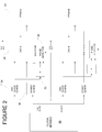
- Figure 2 shows an embodiment of a set of DACs having independent synchronization, making the layout more flexible and having simpler routing paths.
- the common phase detector circuitry of Figure 1 has been removed and instead uses independent, smaller phase detectors such as 32.
- this arrangement allows multiple DACs to be added without requiring a re-design.
- the clock module 30 generates two clocks, a common DAC clock and an internal system reference clock, or SYSREF.
- the SYSREF clock is generated by dividing the DAC clock inside of the clock module.
- the dividers 33 connected to the DAC CLOCK IQ MOD are used to divide the modulated DAC clock down so that it can be accurately compared to SYSREF.
- the DAC clock IQ modulators such as 34 and the SYSREF IQ modulator 36 rotate the DAC clocks and SYSREF clocks, referred to here as the modulated SYSREF clock, going to the DACs and the FPGA to ensure that they are aligned.
- the phase detectors such as 32 monitor the relationship between the two clocks to ensure that the setup and hold windows remain valid
- the setup time is the minimum time before a clock's leading edge in which the data must be valid.
- the hold time is the minimum time after the leading edge for which the data must be valid. For the data outputs to be valid, the set up and hold time windows required for the application or standard under which the system operates must be met.
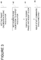
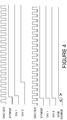
- FIG. 3 shows a flowchart of that process and Figure 4 shows a representational timing diagram.
- the DAC phase calibration value is set to the DAC IQ modulator.
- the process sets the SYSREF phase calibration value to the SYSREF IQ modulator at 42.
- the DACs may not have the same phase relationships between each other, but they will have a leading clock edge that synchronizes with the SYSREF clock.
- the channel-to-channel skew between the DAC clocks will typically end up within 4 DAC clock cycles from each other because the internal divider in the DAC will start up in a random phase.
- the DAC clocks are now shifted to have the same relationship.
- the phase relationship between the DAC clocks and the SYSREF clock is corrected by adjusting the DAC divider phase by rotating the DAC clocks.
- the phase detectors in each channel monitor the relationships between the two clocks to ensure that the desired set up and hold windows are maintained.
- the above synchronization allows the digital signal generators, in this embodiment the FPGAs, to be issued a simultaneous start command at 46 with assurances that the data will be synchronized.
- the individual phase detectors require calibration.
- the calibration process finds the voltage windows for the phase detectors that relates to the correct relationship between the clocks.
- the SYSREF clock is the DAC clock divided by 32, resulting in 32 potential voltage windows considered valid regions.
- the valid regions are then stored in memory for reference during the synchronization process of Figure 5 .
- Figure 5 shows a flow chart of one embodiment of a method to calibrate the phase detectors. This process typically occurs at the factory prior to shipment of the apparatus that uses the synchronized DACs. At 50 a pulse waveform is played and a piece of test equipment such as an oscilloscope is used to test the DAC output. In one embodiment, where the SYSREF clock is divided by 32, a pulse waveform with a width of 1 DAC clock cycle and a total length greater than 64 samples was played.
- the DAC clock phase is aligned to the phase of the internal SYSREF clock in the clock module.
- the modulated SYSREF clock out of the SYSREF IQ MOD is then aligned with a modulated, divided DAC clock out of the DAC CLOCK IQ MOD at 54.
- the SYSREF phase to which it has been aligned is then stored as the calibration value at 56.
- the DACs are synced and adjusted to be at the center of the desired phase.
- the DAC clock phase value after this adjustment is then stored as the calibration value for the DAC clocks and repeated as necessary.
- Examples provide a device, comprising at least two digital-to-analog converters, each digital-to-analog converter having a digital-to-analog converter clock modulator, a system reference clock modulator, and a phase detector to track the phases of the clock and the system reference clock.
- each digital-to-analog converter further comprising a clock divider.
- Some examples further comprise a central clock module to generate a digital-to-analog clock.
- Some examples further comprise a central clock module to generate a system reference clock.
- each digital-to-analog converter may be connected to a device that generates digital signals.
- Examples provide a method of synchronizing digital-to-analog converters in a device, the method comprising setting a phase for digital-to-analog clocks to a phase calibration value, setting a system reference clock to a system reference calibration value, and adjusting the phase relationship between the digital-to-analog clocks and the system reference clock by rotating the digital-to-analog clocks.
- Some examples further comprise issuing a start command to any devices connected to the digital-to-analog converters at a same time.
- Some examples further comprise generating the system reference clock by dividing a central digital-to-analog clock by 32.
- Some examples further comprise monitoring a relationship between the system reference clock and the digital-to-analog converter clock with regard to setup and hold window requirements.
- Examples provide a method of calibrating a phase detector, comprising providing a pulse waveform, aligning a phase of a digital-to-analog clock to a phase of an internal system reference clock, aligning a phase of a modulated system reference clock with a phase of a modulated, divided, digital-to-analog clock, storing the aligned phase of the modulated system reference clock as a calibration value, synchronizing the digital-to-analog converters and adjusting the phase of the digital-to-analog converters to a center of a desired phase, and storing the aligned phase of the digital-to-analog converters as a calibration value.
- the calibrating of the phase detector is repeated as needed.
- the disclosed aspects may be implemented, in some cases, in hardware, firmware, software, or any combination thereof.
- the disclosed aspects may also be implemented as instructions carried by or stored on one or more or computer-readable media, which may be read and executed by one or more processors. Such instructions may be referred to as a computer program product.
- Computer-readable media as discussed herein, means any media that can be accessed by a computing device.
- computer-readable media may comprise computer storage media and communication media.
- Computer storage media means any medium that can be used to store computer-readable information.
- computer storage media may include Random Access Memory (RAM), Read Only Memory (ROM), Electrically Erasable Programmable Read-Only Memory (EEPROM), flash memory or other memory technology, Compact Disc Read Only Memory (CD-ROM), Digital Video Disc (DVD), or other optical disk storage, magnetic cassettes, magnetic tape, magnetic disk storage or other magnetic storage devices, and any other volatile or nonvolatile, removable or non-removable media implemented in any technology.
- Computer storage media excludes signals per se and transitory forms of signal transmission.
- Communication media means any media that can be used for the communication of computer-readable information.
- communication media may include coaxial cables, fiber-optic cables, air, or any other media suitable for the communication of electrical, optical, Radio Frequency (RF), infrared, acoustic or other types of signals.
- RF Radio Frequency
Landscapes
- Engineering & Computer Science (AREA)
- Theoretical Computer Science (AREA)
- Computer Networks & Wireless Communication (AREA)
- Signal Processing (AREA)
- Stabilization Of Oscillater, Synchronisation, Frequency Synthesizers (AREA)
- Analogue/Digital Conversion (AREA)
Abstract
Description
- This disclosure relates to digital-to-analog converters, more particularly to synchronizing multiple digital-to-analog converters in a device.
- Digital-to-analog (DAC) converters have many applications, among them testing equipment and wave generators, which are sometimes also used in testing equipment. All the DACs in the device are synchronized using common phase detector hardware that measures the relationships between all the DAC outputs. The clocks are shifted until they are all aligned and the outputs of the DACs become de-skewed.
- Issues arise in this method of synchronization because each DAC module need to have connections to the common phase detector circuit. This results in extra routing traces and less flexibility and re-use. If a system designer wanted extra channels, the phase detector would have to change to accommodate the extra DACs for the extra channels.
- One embodiment is a device including at least two digital-to-analog converters, each digital-to-analog converter having a digital-to-analog converter clock modulator, a system reference clock modulator, and a phase detector to track the phases of the clock and the system reference clock.
- Another embodiment is a method of calibrating a phase detector including providing a pulse waveform, aligning a phase of a digital-to-analog clock to a phase of an internal system reference clock, aligning a phase of a modulated system reference clock with a phase of a modulated, divided, digital-to-analog clock, storing the aligned phase of the modulated system reference clock as a calibration value, synchronizing the digital-to-analog converters and adjusting the phase of the digital-to-analog converters to a center of a desired phase, and storing the aligned phase of the digital-to-analog converters as a calibration value.
-
-
Figure 1 shows a prior art implementation of a dual channel system having a common phase detector -
Figure 2 shows an embodiment of a system having independent digital-to-analog converter synchronization. -
Figure 3 shows a flowchart of one embodiment of a method to synchronize digital-to-analog converters. -
Figure 4 shows a timing diagram of a pulse waveforms in a synchronization process. -
Figure 5 shows a flowchart of one embodiment of a method to calibrate a phase detector. -
Figure 1 shows a prior art example of a typical set of digital-to-analog converters (DACs) and a centralized phase detector. The example shown has two DACs,DAC A 18, and DAC B. This discussion will only focus onDAC A 18, with the understanding that the same discussion applies to DAC B. Each DAC has a connection to aclock module 10 that generates a system clock. The clock is provided to an IQ modulator for each DAC to produce a DAC clock. - The IQ modulator modulates the in-phase (I) and quadrature (Q) phases of the DAC clock to rotate them according to a desired phase. The term 'rotate' is used because the IQ signals are typically plotted on a polar axis, but may also be thought of delaying or shifting the phase of the signals. In the system of
Figure 1 , thephase detector 12 receives each of the DAC clock signals from the DACs such as 18 divided by 16. The phase detector then measures the relationships between all the DAC clocks. The voltage of the phase detector is compared to a known calibration value. When the measured voltage equals the calibration value, the DAC clocks are aligned and the outputs are de-skewed. - The voltage calibration value is used as a starting point. The process 'rotates,' or shifts, the clock so that it reaches the desired phase detector voltage, then it does a fine adjustment on the clock to the desired phase. The phase detector voltage would not match the calibration voltage value. One should note that the DAC here is attached to an FPGA 20 (field-programmable gate array) that generates the original digital signal that undergoes conversion.
- This synchronization method relies upon the calibration of the phase detector. To calibrate the phase detector, a test waveform is generated and test equipment, such as an oscilloscope measure the outputs of each DAC. The outputs are de-skewed. Delays sometimes exist in the output signals, meaning that some signals are delayed compared to other signals. De-skewing typically compensates for that delay by slowing down the faster signals such that all signals synchronize. This may also be referred to as aligning the signals. Once all the signals are aligned, the phase detector voltages are measured and stored in memory. These become the calibration values mentioned above.
- The issue with a single phase detector for the DAC clocks lies in the lack of flexibility as well as the extra routing paths. If one were to add another channel, requiring another DAC, the phase detector circuit must be re-designed to accommodate the new channel. Further, the connection between each DAC clock back to the phase detector requires extra routing, complicating the layout of the circuit.
- In contrast to the prior art of
Figure 1 ,Figure 2 shows an embodiment of a set of DACs having independent synchronization, making the layout more flexible and having simpler routing paths. The common phase detector circuitry ofFigure 1 has been removed and instead uses independent, smaller phase detectors such as 32. UnlikeFigure 1 , where the number of channels, and therefore DACs, is fixed for a particular phase detector, this arrangement allows multiple DACs to be added without requiring a re-design. - To ensure synchronization, it is important that all the devices operate off the same clock source. The
clock module 30 generates two clocks, a common DAC clock and an internal system reference clock, or SYSREF. The SYSREF clock is generated by dividing the DAC clock inside of the clock module. There are internal dividers in the clock module that divide the DAC clock and generate what will be referred to here as the internal SYSREF. Thedividers 33 connected to the DAC CLOCK IQ MOD are used to divide the modulated DAC clock down so that it can be accurately compared to SYSREF. The DAC clock IQ modulators such as 34 and the SYSREFIQ modulator 36 rotate the DAC clocks and SYSREF clocks, referred to here as the modulated SYSREF clock, going to the DACs and the FPGA to ensure that they are aligned. The phase detectors such as 32 monitor the relationship between the two clocks to ensure that the setup and hold windows remain valid - The setup time is the minimum time before a clock's leading edge in which the data must be valid. Similarly, the hold time is the minimum time after the leading edge for which the data must be valid. For the data outputs to be valid, the set up and hold time windows required for the application or standard under which the system operates must be met.
- With the independent phase detectors, the synchronization process now operates differently than it would for the circuit of
Figure 1 .Figure 3 shows a flowchart of that process andFigure 4 shows a representational timing diagram. At 40, the DAC phase calibration value is set to the DAC IQ modulator. As will be discussed further, there is a DAC phase calibration value set during calibration. - Similarly, the process sets the SYSREF phase calibration value to the SYSREF IQ modulator at 42. Referring to
Figure 4 , one can see that DAC clock, the SYSREF clock and two of the DAC divided clocks DIV1 and DIV2. The DACs may not have the same phase relationships between each other, but they will have a leading clock edge that synchronizes with the SYSREF clock. The channel-to-channel skew between the DAC clocks will typically end up within 4 DAC clock cycles from each other because the internal divider in the DAC will start up in a random phase. - The DAC clocks are now shifted to have the same relationship. One may think of this as all the DAC clocks having the same starting point. Previously, for example, all the DAC clocks may have had a leading edge at a particular point in time, but for some of the DACs, it could have been t = 2, and for another DAC, it may have been t = 0. Shifting the DAC clocks to have the same phase relationship with the SYSREF clock puts them all at the same point in time. This causes the all the DACs to be synchronized. This is shown in the lower diagram of
Figure 4 . - At 44, the phase relationship between the DAC clocks and the SYSREF clock is corrected by adjusting the DAC divider phase by rotating the DAC clocks. As mentioned above, the phase detectors in each channel monitor the relationships between the two clocks to ensure that the desired set up and hold windows are maintained. The above synchronization allows the digital signal generators, in this embodiment the FPGAs, to be issued a simultaneous start command at 46 with assurances that the data will be synchronized.
- The individual phase detectors require calibration. The calibration process finds the voltage windows for the phase detectors that relates to the correct relationship between the clocks. In one embodiment, the SYSREF clock is the DAC clock divided by 32, resulting in 32 potential voltage windows considered valid regions. The valid regions are then stored in memory for reference during the synchronization process of
Figure 5 . -
Figure 5 shows a flow chart of one embodiment of a method to calibrate the phase detectors. This process typically occurs at the factory prior to shipment of the apparatus that uses the synchronized DACs. At 50 a pulse waveform is played and a piece of test equipment such as an oscilloscope is used to test the DAC output. In one embodiment, where the SYSREF clock is divided by 32, a pulse waveform with a width of 1 DAC clock cycle and a total length greater than 64 samples was played. - At 52, the DAC clock phase is aligned to the phase of the internal SYSREF clock in the clock module. The modulated SYSREF clock out of the SYSREF IQ MOD is then aligned with a modulated, divided DAC clock out of the DAC CLOCK IQ MOD at 54. The SYSREF phase to which it has been aligned is then stored as the calibration value at 56. At 58 the DACs are synced and adjusted to be at the center of the desired phase. The DAC clock phase value after this adjustment is then stored as the calibration value for the DAC clocks and repeated as necessary.
- In this manner, a more flexible architecture for DACs synchronization can be achieved. Having independent, more modular, DAC channels with their own phase detectors allows for additional channels to be added without having to redesign the phase detector. Eliminating the routing of signals to a central phase detector from each DAC also simplifies the routing, reducing the complexity of the circuit.
- Examples provide a device, comprising at least two digital-to-analog converters, each digital-to-analog converter having a digital-to-analog converter clock modulator, a system reference clock modulator, and a phase detector to track the phases of the clock and the system reference clock.
- In some examples, each digital-to-analog converter further comprising a clock divider.
- Some examples further comprise a central clock module to generate a digital-to-analog clock.
- Some examples further comprise a central clock module to generate a system reference clock.
- In some examples, each digital-to-analog converter may be connected to a device that generates digital signals.
- Examples provide a method of synchronizing digital-to-analog converters in a device, the method comprising setting a phase for digital-to-analog clocks to a phase calibration value, setting a system reference clock to a system reference calibration value, and adjusting the phase relationship between the digital-to-analog clocks and the system reference clock by rotating the digital-to-analog clocks.
- Some examples further comprise issuing a start command to any devices connected to the digital-to-analog converters at a same time.
- Some examples further comprise generating the system reference clock by dividing a central digital-to-analog clock by 32.
- Some examples further comprise monitoring a relationship between the system reference clock and the digital-to-analog converter clock with regard to setup and hold window requirements.
- Examples provide a method of calibrating a phase detector, comprising providing a pulse waveform, aligning a phase of a digital-to-analog clock to a phase of an internal system reference clock, aligning a phase of a modulated system reference clock with a phase of a modulated, divided, digital-to-analog clock, storing the aligned phase of the modulated system reference clock as a calibration value, synchronizing the digital-to-analog converters and adjusting the phase of the digital-to-analog converters to a center of a desired phase, and storing the aligned phase of the digital-to-analog converters as a calibration value.
- In some examples, the calibrating of the phase detector is repeated as needed.
- The disclosed aspects may be implemented, in some cases, in hardware, firmware, software, or any combination thereof. The disclosed aspects may also be implemented as instructions carried by or stored on one or more or computer-readable media, which may be read and executed by one or more processors. Such instructions may be referred to as a computer program product. Computer-readable media, as discussed herein, means any media that can be accessed by a computing device. By way of example, and not limitation, computer-readable media may comprise computer storage media and communication media.
- Computer storage media means any medium that can be used to store computer-readable information. By way of example, and not limitation, computer storage media may include Random Access Memory (RAM), Read Only Memory (ROM), Electrically Erasable Programmable Read-Only Memory (EEPROM), flash memory or other memory technology, Compact Disc Read Only Memory (CD-ROM), Digital Video Disc (DVD), or other optical disk storage, magnetic cassettes, magnetic tape, magnetic disk storage or other magnetic storage devices, and any other volatile or nonvolatile, removable or non-removable media implemented in any technology. Computer storage media excludes signals per se and transitory forms of signal transmission.
- Communication media means any media that can be used for the communication of computer-readable information. By way of example, and not limitation, communication media may include coaxial cables, fiber-optic cables, air, or any other media suitable for the communication of electrical, optical, Radio Frequency (RF), infrared, acoustic or other types of signals.
- Although specific embodiments of the invention have been described for purposes if illustration, it will be understood that various modifications may be made without departing from the scope of the invention.
Claims (11)
- A device, comprising:at least two digital-to-analog converters, each digital-to-analog converter having:a digital-to-analog converter clock modulator;a system reference clock modulator; anda phase detector to track the phases of the clock and the system reference clock.
- The device of claim 1, each digital-to-analog converter further comprising a clock divider.
- The device of claim 1 or 2, further comprising a central clock module to generate a digital-to-analog clock.
- The device of any preceding claim, further comprising a central clock module to generate a system reference clock.
- The device of any preceding claim, each digital-to-analog converter connected to a device that generates digital signals.
- A method of synchronizing digital-to-analog converters in a device, the method comprising:setting a phase for digital-to-analog clocks to a phase calibration value;setting a system reference clock to a system reference calibration value; andadjusting the phase relationship between the digital-to-analog clocks and the system reference clock by rotating the digital-to-analog clocks.
- The method of claim 6, further comprising issuing a start command to any devices connected to the digital-to-analog converters at a same time.
- The method of claim 6 or 7, further comprising generating the system reference clock by dividing a central digital-to-analog clock by 32.
- The method of any of claims 6 to 8, further comprising monitoring a relationship between the system reference clock and the digital-to-analog converter clock with regard to setup and hold window requirements.
- A computer readable storage medium having instructions stored thereon that, when executed by a processor, cause the processor to carry out the calibration of a phase detector, the instructions comprising:playing a pulse waveform;aligning a phase of a digital-to-analog clock to a phase of an internal system reference clock;aligning a phase of a modulated system reference clock with a phase of a modulated, divided, digital-to-analog clock;storing the aligned phase of the modulated system reference clock as a calibration value;synchronizing the digital-to-analog converters and adjusting the phase of the digital-to-analog converters to a center of a desired phase; andstoring the aligned phase of the digital-to-analog converters as a calibration value.
- The method of claim 10, wherein the calibrating of the phase detector is repeated as needed.
Applications Claiming Priority (1)
| Application Number | Priority Date | Filing Date | Title |
|---|---|---|---|
| US15/339,448 US9847787B1 (en) | 2016-10-31 | 2016-10-31 | Independent digital-to-analog converter synchronization |
Publications (1)
| Publication Number | Publication Date |
|---|---|
| EP3316485A1 true EP3316485A1 (en) | 2018-05-02 |
Family
ID=60268220
Family Applications (1)
| Application Number | Title | Priority Date | Filing Date |
|---|---|---|---|
| EP17199418.9A Ceased EP3316485A1 (en) | 2016-10-31 | 2017-10-31 | Independent digital-to-analog converter synchronization |
Country Status (4)
| Country | Link |
|---|---|
| US (1) | US9847787B1 (en) |
| EP (1) | EP3316485A1 (en) |
| JP (1) | JP7090413B2 (en) |
| CN (1) | CN108023591B (en) |
Families Citing this family (6)
| Publication number | Priority date | Publication date | Assignee | Title |
|---|---|---|---|---|
| JP7339727B2 (en) | 2018-04-09 | 2023-09-06 | シャープ株式会社 | User device, control device, and communication control method |
| US11402671B2 (en) | 2019-07-24 | 2022-08-02 | IonQ, Inc. | Scalable and programmable coherent waveform generators |
| FR3100068B1 (en) * | 2019-08-20 | 2021-07-16 | Teledyne E2V Semiconductors Sas | Method for synchronizing analog data at the output of a plurality of digital / analog converters |
| CN110737625B (en) * | 2019-10-12 | 2021-03-23 | 浪潮集团有限公司 | System and method for realizing DAC synchronization in PXIe measurement and control board module |
| US11967968B2 (en) * | 2022-01-28 | 2024-04-23 | Texas Instruments Incorporated | Apparatus and method of over-current limit for multi-channel digital-to-analog converters |
| CN116011574B (en) * | 2022-12-28 | 2025-11-14 | 成都中微达信科技有限公司 | Deterministic delay and arbitrary range delay compensation adjustment device between multiple DA channels |
Citations (3)
| Publication number | Priority date | Publication date | Assignee | Title |
|---|---|---|---|---|
| US7941686B2 (en) * | 2005-08-26 | 2011-05-10 | Tektronix International Sales Gmbh | Phase controllable multichannel signal generator having interleaved digital to analog converters |
| US9083379B2 (en) * | 2013-09-04 | 2015-07-14 | Electronics And Telecommunications Research Institute | System and method for synchronization between digital-to-analog converters (DACs) for high speed signal processing |
| US9225507B1 (en) * | 2013-06-04 | 2015-12-29 | Pmc-Sierra Us, Inc. | System and method for synchronizing local oscillators |
Family Cites Families (9)
| Publication number | Priority date | Publication date | Assignee | Title |
|---|---|---|---|---|
| GB9821091D0 (en) | 1998-09-30 | 1998-11-18 | Koninkl Philips Electronics Nv | Analogue to digital converter |
| US6549157B1 (en) * | 2001-12-18 | 2003-04-15 | Silicon Integrated Systems Corp. | Digital-to-analog converting device and method used in home networking system with compensation mechanism to reduce clock jitter |
| US9086379B2 (en) * | 2004-05-24 | 2015-07-21 | OptoTrace (SuZhou) Technologies, Inc. | System for chemical separation and identification |
| US7079064B1 (en) | 2005-09-26 | 2006-07-18 | Motorola, Inc. | Method and apparatus for phase control of a digital-to-analog converter |
| US7728753B2 (en) * | 2008-10-13 | 2010-06-01 | National Semiconductor Corporation | Continuous synchronization for multiple ADCs |
| CN101621296B (en) * | 2009-08-06 | 2011-12-28 | 北京华力创通科技股份有限公司 | High-speed DAC synchronization method and device |
| CN103595522B (en) * | 2012-08-17 | 2017-03-15 | 北京航天自动控制研究所 | A kind of Dual-channel digital analog converter synchronization method |
| CN103645658B (en) * | 2013-11-25 | 2016-02-10 | 北京经纬恒润科技有限公司 | A kind of phase synchronization method of multi-disc signal converter, device and FPGA controller |
| US9564913B1 (en) * | 2016-03-09 | 2017-02-07 | Analog Devices, Inc. | Synchronization of outputs from multiple digital-to-analog converters |
-
2016
- 2016-10-31 US US15/339,448 patent/US9847787B1/en active Active
-
2017
- 2017-10-31 EP EP17199418.9A patent/EP3316485A1/en not_active Ceased
- 2017-10-31 JP JP2017211184A patent/JP7090413B2/en active Active
- 2017-10-31 CN CN201711048626.XA patent/CN108023591B/en active Active
Patent Citations (3)
| Publication number | Priority date | Publication date | Assignee | Title |
|---|---|---|---|---|
| US7941686B2 (en) * | 2005-08-26 | 2011-05-10 | Tektronix International Sales Gmbh | Phase controllable multichannel signal generator having interleaved digital to analog converters |
| US9225507B1 (en) * | 2013-06-04 | 2015-12-29 | Pmc-Sierra Us, Inc. | System and method for synchronizing local oscillators |
| US9083379B2 (en) * | 2013-09-04 | 2015-07-14 | Electronics And Telecommunications Research Institute | System and method for synchronization between digital-to-analog converters (DACs) for high speed signal processing |
Non-Patent Citations (2)
| Title |
|---|
| JIE WU ET AL: "A low-jitter distributed synchronous clock using DAC", REAL TIME CONFERENCE, 2009. RT '09. 16TH IEEE-NPSS, IEEE, PISCATAWAY, NJ, USA, 10 May 2009 (2009-05-10), pages 532 - 536, XP031562413, ISBN: 978-1-4244-4454-0 * |
| KANG HSIA: "Synchronized Multi-Transmitter Design: Method of Time-aligning Multiple DAC3xJ8xs in JESD204B Environment", 1 March 2016 (2016-03-01), Oxford, XP055453888, ISBN: 978-0-12-397888-2, Retrieved from the Internet <URL:http://www.ti.com/lit/ug/tidubh1/tidubh1.pdf> [retrieved on 20180223] * |
Also Published As
| Publication number | Publication date |
|---|---|
| US9847787B1 (en) | 2017-12-19 |
| JP7090413B2 (en) | 2022-06-24 |
| CN108023591A (en) | 2018-05-11 |
| JP2018074589A (en) | 2018-05-10 |
| CN108023591B (en) | 2024-01-26 |
Similar Documents
| Publication | Publication Date | Title |
|---|---|---|
| US10340931B1 (en) | Dynamic delay adjustment for multi-channel digital-to-analog converter synchronization | |
| US9847787B1 (en) | Independent digital-to-analog converter synchronization | |
| EP2991229B1 (en) | Synchronization for multiple arbitrary waveform generators | |
| CN112214065B (en) | Equipment synchronization calibration method, device, equipment and storage medium | |
| EP4016238B1 (en) | Clock delay detection method and apparatus, clock delay compensation method and apparatus, terminal, and readable storage medium | |
| WO2023130734A1 (en) | Time domain interleaving analog-to-digital converter synchronization method and apparatus | |
| JP7214855B2 (en) | META STABLE STATE DETECTION APPARATUS AND METHOD, ADC CIRCUIT | |
| CN117353748B (en) | Delay correction method and related equipment | |
| JP2017003458A (en) | Sampling circuit, sampling method, and sampling oscilloscope, and waveform display method | |
| CN113252958A (en) | Digital oscilloscope and automatic calibration method for delay difference between channels thereof | |
| CN106612151A (en) | Device and synchronization method for synchronous output between multichannel DDSs | |
| US9083379B2 (en) | System and method for synchronization between digital-to-analog converters (DACs) for high speed signal processing | |
| JP5323826B2 (en) | Method for synchronizing several channel measuring components and / or measuring devices and corresponding measuring device | |
| US10950156B1 (en) | System of multiple timing controllers of a display panel | |
| US20090207901A1 (en) | Delay circuit and method capable of performing online calibration | |
| KR101915900B1 (en) | Programmable power supply and power supply method using the programmable power supply | |
| CN120729317A (en) | A multi-DAC synchronization system for arbitrary waveform generators | |
| CN107769778B (en) | Signal sampling device and signal sampling calibration method | |
| JP5274016B2 (en) | Test apparatus, program, and recording medium | |
| RU2662727C2 (en) | Superhigh-frequency receive/transmit device | |
| CN116953314A (en) | Quantum measurement and control AWG array waveform generation synchronization system | |
| JP2016523030A (en) | Synchronous data system and method for providing phase aligned output data | |
| KR101052282B1 (en) | Clock Synchronizer of Digital High Frequency Memory | |
| CN118300579B (en) | Trigger type signal source, signal generator and multi-signal source synchronization method | |
| US20260088118A1 (en) | Enhanced training for duty cycle adjuster (dca) to minimize jitter in dram transmitter signals |
Legal Events
| Date | Code | Title | Description |
|---|---|---|---|
| PUAI | Public reference made under article 153(3) epc to a published international application that has entered the european phase |
Free format text: ORIGINAL CODE: 0009012 |
|
| STAA | Information on the status of an ep patent application or granted ep patent |
Free format text: STATUS: THE APPLICATION HAS BEEN PUBLISHED |
|
| AK | Designated contracting states |
Kind code of ref document: A1 Designated state(s): AL AT BE BG CH CY CZ DE DK EE ES FI FR GB GR HR HU IE IS IT LI LT LU LV MC MK MT NL NO PL PT RO RS SE SI SK SM TR |
|
| AX | Request for extension of the european patent |
Extension state: BA ME |
|
| STAA | Information on the status of an ep patent application or granted ep patent |
Free format text: STATUS: REQUEST FOR EXAMINATION WAS MADE |
|
| 17P | Request for examination filed |
Effective date: 20181030 |
|
| RBV | Designated contracting states (corrected) |
Designated state(s): AL AT BE BG CH CY CZ DE DK EE ES FI FR GB GR HR HU IE IS IT LI LT LU LV MC MK MT NL NO PL PT RO RS SE SI SK SM TR |
|
| STAA | Information on the status of an ep patent application or granted ep patent |
Free format text: STATUS: EXAMINATION IS IN PROGRESS |
|
| 17Q | First examination report despatched |
Effective date: 20200227 |
|
| STAA | Information on the status of an ep patent application or granted ep patent |
Free format text: STATUS: THE APPLICATION HAS BEEN REFUSED |
|
| 18R | Application refused |
Effective date: 20220510 |