EP3316323A1 - A magnetic random access memory and manufacture thereof - Google Patents
A magnetic random access memory and manufacture thereof Download PDFInfo
- Publication number
- EP3316323A1 EP3316323A1 EP17198887.6A EP17198887A EP3316323A1 EP 3316323 A1 EP3316323 A1 EP 3316323A1 EP 17198887 A EP17198887 A EP 17198887A EP 3316323 A1 EP3316323 A1 EP 3316323A1
- Authority
- EP
- European Patent Office
- Prior art keywords
- layer
- layers
- free
- forming
- fixture
- Prior art date
- Legal status (The legal status is an assumption and is not a legal conclusion. Google has not performed a legal analysis and makes no representation as to the accuracy of the status listed.)
- Withdrawn
Links
Images


Classifications
-
- H—ELECTRICITY
- H10—SEMICONDUCTOR DEVICES; ELECTRIC SOLID-STATE DEVICES NOT OTHERWISE PROVIDED FOR
- H10B—ELECTRONIC MEMORY DEVICES
- H10B61/00—Magnetic memory devices, e.g. magnetoresistive RAM [MRAM] devices
-
- G—PHYSICS
- G11—INFORMATION STORAGE
- G11C—STATIC STORES
- G11C11/00—Digital stores characterised by the use of particular electric or magnetic storage elements; Storage elements therefor
- G11C11/02—Digital stores characterised by the use of particular electric or magnetic storage elements; Storage elements therefor using magnetic elements
- G11C11/16—Digital stores characterised by the use of particular electric or magnetic storage elements; Storage elements therefor using magnetic elements using elements in which the storage effect is based on magnetic spin effect
-
- G—PHYSICS
- G11—INFORMATION STORAGE
- G11C—STATIC STORES
- G11C11/00—Digital stores characterised by the use of particular electric or magnetic storage elements; Storage elements therefor
- G11C11/02—Digital stores characterised by the use of particular electric or magnetic storage elements; Storage elements therefor using magnetic elements
- G11C11/16—Digital stores characterised by the use of particular electric or magnetic storage elements; Storage elements therefor using magnetic elements using elements in which the storage effect is based on magnetic spin effect
- G11C11/161—Digital stores characterised by the use of particular electric or magnetic storage elements; Storage elements therefor using magnetic elements using elements in which the storage effect is based on magnetic spin effect details concerning the memory cell structure, e.g. the layers of the ferromagnetic memory cell
-
- H—ELECTRICITY
- H10—SEMICONDUCTOR DEVICES; ELECTRIC SOLID-STATE DEVICES NOT OTHERWISE PROVIDED FOR
- H10D—INORGANIC ELECTRIC SEMICONDUCTOR DEVICES
- H10D84/00—Integrated devices formed in or on semiconductor substrates that comprise only semiconducting layers, e.g. on Si wafers or on GaAs-on-Si wafers
- H10D84/01—Manufacture or treatment
- H10D84/02—Manufacture or treatment characterised by using material-based technologies
- H10D84/03—Manufacture or treatment characterised by using material-based technologies using Group IV technology, e.g. silicon technology or silicon-carbide [SiC] technology
- H10D84/038—Manufacture or treatment characterised by using material-based technologies using Group IV technology, e.g. silicon technology or silicon-carbide [SiC] technology using silicon technology, e.g. SiGe
-
- H—ELECTRICITY
- H10—SEMICONDUCTOR DEVICES; ELECTRIC SOLID-STATE DEVICES NOT OTHERWISE PROVIDED FOR
- H10D—INORGANIC ELECTRIC SEMICONDUCTOR DEVICES
- H10D88/00—Three-dimensional [3D] integrated devices
- H10D88/01—Manufacture or treatment
-
- H—ELECTRICITY
- H10—SEMICONDUCTOR DEVICES; ELECTRIC SOLID-STATE DEVICES NOT OTHERWISE PROVIDED FOR
- H10N—ELECTRIC SOLID-STATE DEVICES NOT OTHERWISE PROVIDED FOR
- H10N50/00—Galvanomagnetic devices
- H10N50/01—Manufacture or treatment
-
- H—ELECTRICITY
- H10—SEMICONDUCTOR DEVICES; ELECTRIC SOLID-STATE DEVICES NOT OTHERWISE PROVIDED FOR
- H10N—ELECTRIC SOLID-STATE DEVICES NOT OTHERWISE PROVIDED FOR
- H10N50/00—Galvanomagnetic devices
- H10N50/10—Magnetoresistive devices
-
- H—ELECTRICITY
- H10—SEMICONDUCTOR DEVICES; ELECTRIC SOLID-STATE DEVICES NOT OTHERWISE PROVIDED FOR
- H10D—INORGANIC ELECTRIC SEMICONDUCTOR DEVICES
- H10D88/00—Three-dimensional [3D] integrated devices
Definitions
- the present invention relates to semiconductor technologies, more specifically, a magnetic random access memory and its manufacturing method.
- MRAM Magnetic Random Access Memory
- binary data of 0 and 1 can be recorded by different resistances resulting from different magnetization directions, and the resistances will not change as long as the magnetic field is not changed.
- Conventional planar MRAM typically comprises three layers: a free layer connecting a bit line, a fixture layer connecting a word line, and an insulation layer positioned between the free layer and the fixture layer.
- the magnetization direction in the free layer is configurable and the magnetization direction in the fixture layer is fixed.
- a memory unit When the magnetization direction in the free layer is the same as the magnetization direction in the fixture layer, a memory unit has a low resistance and the data 0 is recorded; when the magnetization direction in the free layer is opposite to the magnetization direction in the fixture layer, the memory unit has a high resistance and the data 1 is recorded.
- FIG. 1 shows a schematic cross-sectional view illustrating a conventional 3D MRAM.
- This 3D MRAM has a similar connection structure as that of a planar MRAM. It comprises a fixture layer 101 connecting a word line 105, a free layer 103 connecting a bit line 104, and an insulation layer 102 positioned between the fixture layer 101 and the free layer 103.
- a cavity need to be formed in a dielectric layer 106, and three layers (the fixture layer 101, the insulation layer 102, and the free layer 103 as shown in a dash-line box in Fig.
- ALD Atomic Layer Deposition
- a first aspect of the present invention provides a magnetic random access memory device, comprising: a word line; a bit line; and a memory unit positioned between the word line and the bit line, comprising: a fixture layer connecting the bit line; a free layer connecting the word line; and an insulation layer positioned between the fixture layer and the free layer.
- the aforementioned device may further comprise: a plurality of memory units, wherein the memory units share a fixture layer.
- the memory units may share an insulation layer.
- the neighboring memory units may be separated by the free layers.
- the free layers of the memory units may be arranged along an extension direction of the insulation layer.
- the aforementioned device may further comprise: a plurality of word lines, with each word line connecting the free layer of a corresponding memory unit.
- the aforementioned device may further comprise: dielectric layers positioned between the neighboring free layers.
- the fixture layer may surround an outer surface of the bit line
- the insulation layer may surround an outer surface of the fixture layer
- the free layer may surround an outer surface of the insulation layer.
- the aforementioned device may further comprise: a substrate, wherein the bit lines, the word lines, and the memory units are all positioned on the substrate, and wherein the extension direction of the insulation layer is substantially perpendicular to an upper surface of the substrate.
- the fixture layer may be a magnetic fixture layer and the free layer is a magnetic free layer.
- a second aspect of the present invention provides a method for manufacturing a magnetic random memory device, the method comprising: providing a plurality of sacrificial layers and a plurality of dielectric layers alternately stacking over each other; forming a through-hole by etching the sacrificial layers and the dielectric layers; forming an insulation layer on a side surface of the through-hole; forming a fixture layer on a side surface of the insulation layer; forming a bit line on a side surface of the fixture layer, wherein the bit line filling the through-hole; forming a plurality of cavities by removing the sacrificial layers; and forming a plurality of free layers within the cavities and word lines connecting the free layers, wherein the neighboring free layers are separated by the dielectric layers.
- forming a plurality of cavities by removing sacrificial layers may comprise: forming a groove by etching the sacrificial layers and the dielectric layers; and forming a plurality of cavities by removing the sacrificial layers through the groove.
- forming a plurality of free layers within the cavities and word lines connecting the free layers may comprise: forming free layers on a side surface of the groove and within the cavities; forming a word line metal layer on the free layers filling the groove and the cavities; and forming a plurality of free layers and word lines connecting the free layers by removing the word line metal layer within the groove and a portion of the free layers on a side surface of the groove, wherein the neighboring free layers are separated by the dielectric layers.
- the fixture layer may surround an outer surface of the bit line
- the insulation layer may surround an outer surface of the fixture layer
- the free layer may surround an outer surface of the insulation layer.
- providing a plurality of sacrificial layers and a plurality of dielectric layers alternately stacking over each other may comprise: providing a substrate; and forming a plurality of sacrificial layers and a plurality of dielectric layers alternately stacking over each other on the substrate, forming a through-hole by etching the sacrificial layers and the dielectric layers comprises forming a through-hole to expose an upper surface of the substrate.
- the fixture layer may be a magnetic fixture layer and the free layer is a magnetic free layer.
- a magnetic random memory device according to the first aspect of the present invention may be obtained by a method for manufacturing a magnetic random memory device according to the second aspect of the present invention.
- Embodiments in the figures may represent idealized illustrations. Variations from the shapes illustrated may be possible, for example due to manufacturing techniques and/or tolerances. Thus, the example embodiments shall not be construed as limited to the shapes or regions illustrated herein but are to include deviations in the shapes. For example, an etched region illustrated as a rectangle may have rounded or curved features. The shapes and regions illustrated in the figures are illustrative and shall not limit the invention.
- first,” “second,” etc. may be used herein to describe various elements, these elements shall not be limited by these terms. These terms may be used to distinguish one element from another element. Thus, a first element discussed below may be termed a second element without departing from the teachings of the present inventive concept. The description of an element as a “first” element may not require or imply the presence of a second element or other elements.
- the terms “first,” “second,” etc. may also be used herein to differentiate different categories or sets of elements. For conciseness, the terms “first,” “second,” etc. may represent “first-category (or first-set),” “second-category (or second-set),” etc., respectively.
- first element such as a layer, film, region, or substrate
- neighbored to or “coupled with” a second element
- the first element can be directly on, directly neighboring, directly connected to or directly coupled with the second element, or an intervening element may also be present between the first element and the second element.
- first element is referred to as being “directly on,” “directly neighboring,” “directly connected to,” or “directly coupled with” a second element, then no intended intervening element (except environmental elements such as air) may also be present between the first element and the second element.
- spatially relative terms such as “beneath,” “below,” “lower,” “above,” “upper,” and the like, may be used herein for ease of description to describe one element or feature's spatial relationship to another element(s) or feature(s) as illustrated in the figures. It will be understood that the spatially relative terms may encompass different orientations of the device in use or operation in addition to the orientation depicted in the figures. For example, if the device in the figures is turned over, elements described as “below” or “beneath” other elements or features would then be oriented “above” the other elements or features. Thus, the term “below” can encompass both an orientation of above and below. The device may be otherwise oriented (rotated 90 degrees or at other orientation), and the spatially relative descriptors used herein shall be interpreted accordingly.
- connection may mean “electrically connect.”
- insulation may mean “electrically insulate.”
- Embodiments of the inventive concept may also cover an article of manufacture that includes a non-transitory computer readable medium on which computer-readable instructions for carrying out embodiments of the inventive technique are stored.
- the computer readable medium may include, for example, semiconductor, magnetic, opto-magnetic, optical, or other forms of computer readable medium for storing computer readable code.
- the inventive concept may also cover apparatuses for practicing embodiments of the inventive concept. Such apparatus may include circuits, dedicated and/or programmable, to carry out operations pertaining to embodiments of the inventive concept.
- Examples of such apparatus include a general purpose computer and/or a dedicated computing device when appropriately programmed and may include a combination of a computer/computing device and dedicated/programmable hardware circuits (such as electrical, mechanical, and/or optical circuits) adapted for the various operations pertaining to embodiments of the inventive concept.
- a general purpose computer and/or a dedicated computing device when appropriately programmed and may include a combination of a computer/computing device and dedicated/programmable hardware circuits (such as electrical, mechanical, and/or optical circuits) adapted for the various operations pertaining to embodiments of the inventive concept.
- Fig. 2 shows a flowchart illustrating manufacture procedures of a magnetic random access memory in accordance with one or more embodiments of the present invention.
- Figs. 3, 4 , 5, 6 , 7, 8 , 9, 10 , 11, and 12 show schematic cross-sectional views illustrating different stages of manufacturing a magnetic random access memory in accordance with one or more embodiments of the present invention. Referring to these figures, a manufacturing method of a magnetic random access memory in accordance with one or more embodiments of the present invention is described below.
- step S201 a plurality of sacrificial layers and a plurality of dielectric layers are provided, wherein the sacrificial layers and dielectric layers are alternately stacked over each other.
- step S201 may comprise providing a substrate 300, the substrate 300 may be a silicon substrate or other type of substrate, it may also be a semiconductor structure comprising other structures or layers and is not limited herein.
- step S201 may further comprise forming a plurality of sacrificial layers 320 and a plurality of dielectric layers 310 on the substrate 300, wherein the sacrificial layers 320 and the dielectric layers 310 are stacked alternately over each other, as shown in Fig. 3 .
- the sacrificial layers 320 and the dielectric layers 310 may be made of different materials.
- the sacrificial layers 320 may be made of silicon nitride and the dielectric layers 310 may be made of silicon-based oxide.
- a dielectric layer 310 may first be deposited on the substrate 300, then a sacrificial layer 320 is deposited on that dielectric layer 310, then another dielectric layer 310 is deposited on that sacrificial layer 320, and so on, as shown in Fig. 3 .
- a through-hole is formed by etching the sacrificial layers and the dielectric layers.
- Fig. 4 shows a schematic cross-sectional view illustrating step S202.
- a through-hole 330 may be formed by etching through the sacrificial layers 320 and the dielectric layers 310.
- the through-hole 330 may go through the sacrificial layers 320 and the dielectric layers 310.
- the through-hole 330 may expose an upper surface of the substrate 300.
- step S203 an insulation layer is formed on a side surface of the through-hole.
- Fig. 5 shows a schematic cross-sectional view illustrating step S203.
- an insulation layer 302 may be formed on a side surface of the through-hole 330 by Atomic Layer Deposition (ALD).
- Step S203 may comprise forming the insulation layer 302 on the side surface and the bottom of the through-hole 330.
- step S203 may further comprise removing a portion of the insulation layer 302 on the bottom of the through-hole 330 while retaining a portion of the insulation layer 302 on the side surface of the through-hole 330.
- step S204 a fixture layer is formed on a side surface of the insulation layer.
- Fig. 6 shows a schematic cross-sectional view illustrating step S204.
- a fixture layer 301 may be formed on a side surface of the insulation layer 302 by ALD.
- the fixture layer 301 may be a magnetic fixture layer.
- step S204 may comprise forming the fixture layer 301 on the side surface of the insulation layer 302 and on the bottom of the through-hole 330.
- step S204 may further comprise removing a portion of the fixture layer 301 on the bottom of the through-hole 330 by an etching process.
- step S205 a bit line filling the through-hole is formed on a side surface of the fixture layer.
- Fig. 7 shows a schematic cross-sectional view illustrating step S205.
- a bit line 304 may be formed on a side surface of the fixture layer 301 by filling the through-hole 330.
- step S205 may comprise depositing a bit line material layer on the structure shown in Fig. 6 , wherein the bit line material layer fills the through-hole 330 and covers an upper surface of the top-most sacrificial layer 320.
- step S205 may further comprise performing a planarization process on the bit line material layer to remove a portion of the bit line material layer on the upper surface of the top-most sacrificial layer 320, the rest of the bit line material layer fills the through-hole 330 and forms the bit line 304.
- step S206 the sacrificial layers are removed to form a plurality of cavities.
- step S206 comprises etching through the sacrificial layers 320 and the dielectric layers 310 to form a groove 333.
- the groove 333 may expose the upper surface of the substrate 300.
- step S206 may further comprise performing a wet etching process through the groove 333 to remove the sacrificial layers 320 to form a plurality of cavities 340.
- the cavities 340 extend in a plane that is parallel to the surface of the substrate 300 on which the dielectric layer 310 is formed, and have openings on the side wall.
- step S207 a plurality of free layers are formed in the cavities and word lines connecting the free layers are formed, with the free layers being separated by the dielectric layers.
- step S207 may comprise forming a plurality of free layers 303 on a side surface of the groove 333 and within the cavities 340 by ALD.
- the free layers 303 may be magnetic free layers.
- step S207 may further comprise depositing a word line metal layer 305 on the free layers 303 filling the groove 333 and the cavities 340.
- step S207 may further comprise etching away a portion of the word line metal layer 305 within the groove 333 and a portion of the free layers 303 on the side surface of the groove 333. This process results in a plurality of free layers 303 that are separated by the dielectric layers 310 and a plurality of word lines 305 each connecting a corresponding free layer 303.
- the fixture layers 301 surrounds an outer surface of the bit line 304
- the insulation layers 302 surrounds an outer surface of the fixture layer 301
- the free layers 303 surrounds an outer surface of the insulation layer 302.
- This method manufactures a magnetic random access memory, such as a 3D MRAM.
- the free layers are formed within the cavities between the dielectric layers, and there is no insulation layer or fixture layer in the cavities, this simplifies the manufacturing process and the structure of the resulted magnetic random access memory. Additionally, the reduction of the layers within the cavities reduces the manufacturing defect within the cavities and improves the performance of the end product.
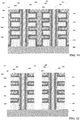
- FIG. 12 shows two magnetic random access memory in accordance to one or more embodiments of the present invention. Referring to Fig. 12 , a magnetic random access memory in accordance with one or more embodiments of the present invention is described below.
- a magnetic random access memory comprises a word line 305, a bit line 304, and a memory unit 350 located between the word line 305 and the bit line 304, as shown in a dash-line box in Fig. 12 .
- the memory unit 350 may comprise a fixture layer 301 connecting the bit line 304, a free layer 303 connecting the word line 305, and an insulation layer 302 positioned between the fixture layer 301 and the free layer 303.
- the fixture layer 301 may be a magnetic fixture layer and the free layer 303 may be a magnetic free layer.
- the fixture layer 301 surrounds an outer surface of the bit line 304
- the insulation layer 302 surrounds an outer surface of the fixture layer 301
- the free layer 303 surrounds an outer surface of the insulation layer 302.
- the magnetic random access memory device shown in Fig. 12 is a 3D magnetic random access memory.
- the magnetic random access memory may comprise a plurality of memory units 350.
- the memory units 350 may share a common fixture layer 301, the memory units 350 may also share a common insulation layer 302. This simplifies the structure of the magnetic random access memory.
- neighboring memory units 350 are separated by the free layers 303.
- the magnetic random access memory may further comprise the dielectric layers 310 located between and separating the neighboring free layers 303.
- the magnetic random access memory may comprise a plurality of word lines 305, with each word line 305 connecting a free layer 303 of a corresponding memory unit 350.
- the free layers 303 of the memory units 350 are arranged along an extension direction of the insulation layer 302.
- the magnetic random access memory may further comprise a substrate 300, wherein the word line 305, the bit line 304, and the memory unit 350 are all on the substrate 300.
- the extension direction of the insulation layer 302 is substantially perpendicular to an upper surface of the substrate 300.
- the magnetic random access memory in accordance with this one or more embodiments of the present invention has a simple structure, which simplifies the manufacturing procedure and improves its integration level. Additionally, it also provides an improved performance compared to conventional magnetic random access memories.
Landscapes
- Engineering & Computer Science (AREA)
- Computer Hardware Design (AREA)
- Manufacturing & Machinery (AREA)
- Hall/Mr Elements (AREA)
- Mram Or Spin Memory Techniques (AREA)
Abstract
Description
- This application claims priority to and benefit of Chinese Patent Application No.
201610925894.4 filed on October 31, 2016 - The present invention relates to semiconductor technologies, more specifically, a magnetic random access memory and its manufacturing method.
- Magnetic Random Access Memory (MRAM) uses resistance characteristic of a magnetic field to record data. In MRAM, binary data of 0 and 1 can be recorded by different resistances resulting from different magnetization directions, and the resistances will not change as long as the magnetic field is not changed.
- Conventional planar MRAM typically comprises three layers: a free layer connecting a bit line, a fixture layer connecting a word line, and an insulation layer positioned between the free layer and the fixture layer. The magnetization direction in the free layer is configurable and the magnetization direction in the fixture layer is fixed. When the magnetization direction in the free layer is the same as the magnetization direction in the fixture layer, a memory unit has a low resistance and the data 0 is recorded; when the magnetization direction in the free layer is opposite to the magnetization direction in the fixture layer, the memory unit has a high resistance and the data 1 is recorded.
- With the advancement of technical specification, the limitations of existing planar MRAMs are becoming more cumbersome and 3-dimensional (3D) MRAM is becoming a more attractive choice.
Fig. 1 shows a schematic cross-sectional view illustrating a conventional 3D MRAM. This 3D MRAM has a similar connection structure as that of a planar MRAM. It comprises afixture layer 101 connecting aword line 105, afree layer 103 connecting abit line 104, and aninsulation layer 102 positioned between thefixture layer 101 and thefree layer 103. To manufacture this 3D MRAM, a cavity need to be formed in adielectric layer 106, and three layers (thefixture layer 101, theinsulation layer 102, and thefree layer 103 as shown in a dash-line box inFig. 1 ) need to be formed by Atomic Layer Deposition (ALD) within the cavity. This is a difficult manufacturing process and the layers formed in a concave area, even for those formed by ALD, are prone to manufacturing defects, which deteriorate the performance of the resulted semiconductor devices. - It is an object of the present invention to provide a magnetic random access memory device and a method for manufacturing a magnetic random memory device which may solve one or more of the above discussed or other problems in the prior art.
- The object is achieved by the features of the respective independent claims. Further embodiments are defined in the respective dependent claims.
- A first aspect of the present invention provides a magnetic random access memory device, comprising: a word line; a bit line; and a memory unit positioned between the word line and the bit line, comprising: a fixture layer connecting the bit line; a free layer connecting the word line; and an insulation layer positioned between the fixture layer and the free layer.
- Preferably, the aforementioned device may further comprise: a plurality of memory units, wherein the memory units share a fixture layer.
- Preferably, in the aforementioned device, the memory units may share an insulation layer.
- Preferably, in the aforementioned device, the neighboring memory units may be separated by the free layers.
- Preferably, in the aforementioned device, the free layers of the memory units may be arranged along an extension direction of the insulation layer.
- Preferably, the aforementioned device may further comprise: a plurality of word lines, with each word line connecting the free layer of a corresponding memory unit.
- Preferably, the aforementioned device may further comprise: dielectric layers positioned between the neighboring free layers.
- Preferably, in the aforementioned device, the fixture layer may surround an outer surface of the bit line, the insulation layer may surround an outer surface of the fixture layer, and the free layer may surround an outer surface of the insulation layer.
- Preferably, the aforementioned device may further comprise: a substrate, wherein the bit lines, the word lines, and the memory units are all positioned on the substrate, and wherein the extension direction of the insulation layer is substantially perpendicular to an upper surface of the substrate.
- Preferably, in the aforementioned device, the fixture layer may be a magnetic fixture layer and the free layer is a magnetic free layer.
- A second aspect of the present invention provides a method for manufacturing a magnetic random memory device, the method comprising: providing a plurality of sacrificial layers and a plurality of dielectric layers alternately stacking over each other; forming a through-hole by etching the sacrificial layers and the dielectric layers; forming an insulation layer on a side surface of the through-hole; forming a fixture layer on a side surface of the insulation layer; forming a bit line on a side surface of the fixture layer, wherein the bit line filling the through-hole; forming a plurality of cavities by removing the sacrificial layers; and forming a plurality of free layers within the cavities and word lines connecting the free layers, wherein the neighboring free layers are separated by the dielectric layers.
- Preferably, in the aforementioned method, forming a plurality of cavities by removing sacrificial layers may comprise: forming a groove by etching the sacrificial layers and the dielectric layers; and forming a plurality of cavities by removing the sacrificial layers through the groove.
- Preferably, in the aforementioned method, forming a plurality of free layers within the cavities and word lines connecting the free layers may comprise: forming free layers on a side surface of the groove and within the cavities; forming a word line metal layer on the free layers filling the groove and the cavities; and forming a plurality of free layers and word lines connecting the free layers by removing the word line metal layer within the groove and a portion of the free layers on a side surface of the groove, wherein the neighboring free layers are separated by the dielectric layers.
- Preferably, in the aforementioned method, the fixture layer may surround an outer surface of the bit line, the insulation layer may surround an outer surface of the fixture layer, and the free layer may surround an outer surface of the insulation layer.
- Preferably, in the aforementioned method, providing a plurality of sacrificial layers and a plurality of dielectric layers alternately stacking over each other may comprise: providing a substrate; and forming a plurality of sacrificial layers and a plurality of dielectric layers alternately stacking over each other on the substrate, forming a through-hole by etching the sacrificial layers and the dielectric layers comprises forming a through-hole to expose an upper surface of the substrate.
- Preferably, in the aforementioned method, the fixture layer may be a magnetic fixture layer and the free layer is a magnetic free layer.
- A magnetic random memory device according to the first aspect of the present invention may be obtained by a method for manufacturing a magnetic random memory device according to the second aspect of the present invention.
-
-
Fig. 1 shows a schematic cross-sectional view illustrating a conventional 3D magnetic random access memory. -
Fig. 2 shows a flowchart illustrating manufacture procedures of a magnetic random access memory in accordance with one or more embodiments of the present invention. -
Figs. 3, 4 ,5, 6 ,7, 8 ,9, 10 ,11, and 12 show schematic cross-sectional views illustrating different stages of manufacturing a magnetic random access memory in accordance with one or more embodiments of the present invention. - Example embodiments of the inventive concept are described with reference to the accompanying drawings. Embodiments may be practiced without some or all of these specified details. Well known process steps and/or structures may not be described in detail, in the interest of clarity.
- The drawings and descriptions are illustrative and not restrictive. Like reference numerals may designate like (e.g., analogous or identical) elements in the specification. To the extent possible, any repetitive description will be minimized.
- Relative sizes and thicknesses of elements shown in the drawings are chosen to facilitate description and understanding, without limiting the inventive concept. In the drawings, the thicknesses of some layers, films, panels, regions, etc., may be exaggerated for clarity.
- Embodiments in the figures may represent idealized illustrations. Variations from the shapes illustrated may be possible, for example due to manufacturing techniques and/or tolerances. Thus, the example embodiments shall not be construed as limited to the shapes or regions illustrated herein but are to include deviations in the shapes. For example, an etched region illustrated as a rectangle may have rounded or curved features. The shapes and regions illustrated in the figures are illustrative and shall not limit the invention.
- Although the terms "first," "second," etc. may be used herein to describe various elements, these elements shall not be limited by these terms. These terms may be used to distinguish one element from another element. Thus, a first element discussed below may be termed a second element without departing from the teachings of the present inventive concept. The description of an element as a "first" element may not require or imply the presence of a second element or other elements. The terms "first," "second," etc. may also be used herein to differentiate different categories or sets of elements. For conciseness, the terms "first," "second," etc. may represent "first-category (or first-set)," "second-category (or second-set)," etc., respectively.
- If a first element (such as a layer, film, region, or substrate) is referred to as being "on," "neighboring," "connected to," or "coupled with" a second element, then the first element can be directly on, directly neighboring, directly connected to or directly coupled with the second element, or an intervening element may also be present between the first element and the second element. If a first element is referred to as being "directly on," "directly neighboring," "directly connected to," or "directly coupled with" a second element, then no intended intervening element (except environmental elements such as air) may also be present between the first element and the second element.
- Spatially relative terms, such as "beneath," "below," "lower," "above," "upper," and the like, may be used herein for ease of description to describe one element or feature's spatial relationship to another element(s) or feature(s) as illustrated in the figures. It will be understood that the spatially relative terms may encompass different orientations of the device in use or operation in addition to the orientation depicted in the figures. For example, if the device in the figures is turned over, elements described as "below" or "beneath" other elements or features would then be oriented "above" the other elements or features. Thus, the term "below" can encompass both an orientation of above and below. The device may be otherwise oriented (rotated 90 degrees or at other orientation), and the spatially relative descriptors used herein shall be interpreted accordingly.
- The terminology used herein is for the purpose of describing particular embodiments and is not intended to limit the inventive concept. As used herein, singular forms, "a," "an," and "the" may indicate plural forms as well, unless the context clearly indicates otherwise. The terms "includes" and/or "including," when used in this specification, may specify the presence of stated features, integers, steps, operations, elements, and/or components, but may not preclude the presence or addition of one or more other features, integers, steps, operations, elements, components, and/or groups.
- Unless otherwise defined, terms (including technical and scientific terms) used herein have the same meanings as what is commonly understood by one of ordinary skill in the art related to this field. Terms, such as those defined in commonly used dictionaries, shall be interpreted as having meanings that are consistent with their meanings in the context of the relevant art and shall not be interpreted in an idealized or overly formal sense unless expressly so defined herein.
- The term "connect" may mean "electrically connect." The term "insulate" may mean "electrically insulate."
- Unless explicitly described to the contrary, the word "comprise" and variations such as "comprises," "comprising," "include," or "including" may imply the inclusion of stated elements but not the exclusion of other elements.
- Various embodiments, including methods and techniques, are described in this disclosure. Embodiments of the inventive concept may also cover an article of manufacture that includes a non-transitory computer readable medium on which computer-readable instructions for carrying out embodiments of the inventive technique are stored. The computer readable medium may include, for example, semiconductor, magnetic, opto-magnetic, optical, or other forms of computer readable medium for storing computer readable code. Further, the inventive concept may also cover apparatuses for practicing embodiments of the inventive concept. Such apparatus may include circuits, dedicated and/or programmable, to carry out operations pertaining to embodiments of the inventive concept. Examples of such apparatus include a general purpose computer and/or a dedicated computing device when appropriately programmed and may include a combination of a computer/computing device and dedicated/programmable hardware circuits (such as electrical, mechanical, and/or optical circuits) adapted for the various operations pertaining to embodiments of the inventive concept.
-
Fig. 2 shows a flowchart illustrating manufacture procedures of a magnetic random access memory in accordance with one or more embodiments of the present invention.Figs. 3, 4 ,5, 6 ,7, 8 ,9, 10 ,11, and 12 show schematic cross-sectional views illustrating different stages of manufacturing a magnetic random access memory in accordance with one or more embodiments of the present invention. Referring to these figures, a manufacturing method of a magnetic random access memory in accordance with one or more embodiments of the present invention is described below. - Referring to
Fig. 2 , in step S201, a plurality of sacrificial layers and a plurality of dielectric layers are provided, wherein the sacrificial layers and dielectric layers are alternately stacked over each other. -
Fig. 3 shows a schematic cross-sectional view illustrating step S201. Referring toFig. 3 , step S201 may comprise providing asubstrate 300, thesubstrate 300 may be a silicon substrate or other type of substrate, it may also be a semiconductor structure comprising other structures or layers and is not limited herein. Optionally, step S201 may further comprise forming a plurality ofsacrificial layers 320 and a plurality ofdielectric layers 310 on thesubstrate 300, wherein thesacrificial layers 320 and thedielectric layers 310 are stacked alternately over each other, as shown inFig. 3 . Thesacrificial layers 320 and thedielectric layers 310 may be made of different materials. For example, thesacrificial layers 320 may be made of silicon nitride and thedielectric layers 310 may be made of silicon-based oxide. In step S201, adielectric layer 310 may first be deposited on thesubstrate 300, then asacrificial layer 320 is deposited on thatdielectric layer 310, then anotherdielectric layer 310 is deposited on thatsacrificial layer 320, and so on, as shown inFig. 3 . - Referring to
Fig. 2 , in step S202, a through-hole is formed by etching the sacrificial layers and the dielectric layers. -
Fig. 4 shows a schematic cross-sectional view illustrating step S202. Referring toFig. 4 , a through-hole 330 may be formed by etching through thesacrificial layers 320 and the dielectric layers 310. The through-hole 330 may go through thesacrificial layers 320 and the dielectric layers 310. Optionally, as shown inFig. 4 , the through-hole 330 may expose an upper surface of thesubstrate 300. - Referring to
Fig. 2 , in step S203, an insulation layer is formed on a side surface of the through-hole. -
Fig. 5 shows a schematic cross-sectional view illustrating step S203. Referring toFig. 5 , aninsulation layer 302 may be formed on a side surface of the through-hole 330 by Atomic Layer Deposition (ALD). Step S203 may comprise forming theinsulation layer 302 on the side surface and the bottom of the through-hole 330. Optionally, step S203 may further comprise removing a portion of theinsulation layer 302 on the bottom of the through-hole 330 while retaining a portion of theinsulation layer 302 on the side surface of the through-hole 330. - Referring to
Fig. 2 , in step S204, a fixture layer is formed on a side surface of the insulation layer. -
Fig. 6 shows a schematic cross-sectional view illustrating step S204. Referring toFig. 6 , afixture layer 301 may be formed on a side surface of theinsulation layer 302 by ALD. Thefixture layer 301 may be a magnetic fixture layer. Optionally, step S204 may comprise forming thefixture layer 301 on the side surface of theinsulation layer 302 and on the bottom of the through-hole 330. Optionally, step S204 may further comprise removing a portion of thefixture layer 301 on the bottom of the through-hole 330 by an etching process. - Referring to
Fig. 2 , in step S205, a bit line filling the through-hole is formed on a side surface of the fixture layer. -
Fig. 7 shows a schematic cross-sectional view illustrating step S205. Referring toFig. 7 , abit line 304 may be formed on a side surface of thefixture layer 301 by filling the through-hole 330. Optionally, step S205 may comprise depositing a bit line material layer on the structure shown inFig. 6 , wherein the bit line material layer fills the through-hole 330 and covers an upper surface of the top-mostsacrificial layer 320. Optionally, step S205 may further comprise performing a planarization process on the bit line material layer to remove a portion of the bit line material layer on the upper surface of the top-mostsacrificial layer 320, the rest of the bit line material layer fills the through-hole 330 and forms thebit line 304. - Referring to
Fig. 2 , in step S206, the sacrificial layers are removed to form a plurality of cavities. -
Figs. 8 and9 show schematic cross-sectional views illustrating different stages of step S206. Referring toFig. 8 , step S206 comprises etching through thesacrificial layers 320 and thedielectric layers 310 to form agroove 333. Thegroove 333 may expose the upper surface of thesubstrate 300. Referring toFig. 9 , step S206 may further comprise performing a wet etching process through thegroove 333 to remove thesacrificial layers 320 to form a plurality ofcavities 340. Thecavities 340 extend in a plane that is parallel to the surface of thesubstrate 300 on which thedielectric layer 310 is formed, and have openings on the side wall. - Referring to
Fig. 2 , in step S207, a plurality of free layers are formed in the cavities and word lines connecting the free layers are formed, with the free layers being separated by the dielectric layers. -
Figs. 10 ,11 and 12 show schematic cross-sectional views illustrating different stages of step S207. Referring toFig. 10 , step S207 may comprise forming a plurality offree layers 303 on a side surface of thegroove 333 and within thecavities 340 by ALD. Thefree layers 303 may be magnetic free layers. Referring toFig. 11 , step S207 may further comprise depositing a wordline metal layer 305 on thefree layers 303 filling thegroove 333 and thecavities 340. Referring toFig. 12 , step S207 may further comprise etching away a portion of the wordline metal layer 305 within thegroove 333 and a portion of thefree layers 303 on the side surface of thegroove 333. This process results in a plurality offree layers 303 that are separated by thedielectric layers 310 and a plurality ofword lines 305 each connecting a correspondingfree layer 303. - In this manufacturing process, the fixture layers 301 surrounds an outer surface of the
bit line 304, the insulation layers 302 surrounds an outer surface of thefixture layer 301, and thefree layers 303 surrounds an outer surface of theinsulation layer 302. - This concludes a manufacturing method of a magnetic random access memory in accordance with one or more embodiments of the present invention. This method manufactures a magnetic random access memory, such as a 3D MRAM. In this manufacturing method, the free layers are formed within the cavities between the dielectric layers, and there is no insulation layer or fixture layer in the cavities, this simplifies the manufacturing process and the structure of the resulted magnetic random access memory. Additionally, the reduction of the layers within the cavities reduces the manufacturing defect within the cavities and improves the performance of the end product.
- This application further presents a magnetic random access memory.
Fig. 12 shows two magnetic random access memory in accordance to one or more embodiments of the present invention. Referring toFig. 12 , a magnetic random access memory in accordance with one or more embodiments of the present invention is described below. - Referring to
Fig. 12 , a magnetic random access memory comprises aword line 305, abit line 304, and amemory unit 350 located between theword line 305 and thebit line 304, as shown in a dash-line box inFig. 12 . Thememory unit 350 may comprise afixture layer 301 connecting thebit line 304, afree layer 303 connecting theword line 305, and aninsulation layer 302 positioned between thefixture layer 301 and thefree layer 303. As an example, thefixture layer 301 may be a magnetic fixture layer and thefree layer 303 may be a magnetic free layer. - Referring to
Fig. 12 , in one embodiment, thefixture layer 301 surrounds an outer surface of thebit line 304, theinsulation layer 302 surrounds an outer surface of thefixture layer 301, and thefree layer 303 surrounds an outer surface of theinsulation layer 302. The magnetic random access memory device shown inFig. 12 is a 3D magnetic random access memory. - Referring to
Fig. 12 , in one embodiment, the magnetic random access memory may comprise a plurality ofmemory units 350. Thememory units 350 may share acommon fixture layer 301, thememory units 350 may also share acommon insulation layer 302. This simplifies the structure of the magnetic random access memory. - Referring to
Fig. 12 , in one embodiment, neighboringmemory units 350 are separated by the free layers 303. The magnetic random access memory may further comprise thedielectric layers 310 located between and separating the neighboringfree layers 303. - Referring to
Fig. 12 , in one embodiment, the magnetic random access memory may comprise a plurality ofword lines 305, with eachword line 305 connecting afree layer 303 of acorresponding memory unit 350. Thefree layers 303 of thememory units 350 are arranged along an extension direction of theinsulation layer 302. - Referring to
Fig. 12 , in one embodiment, the magnetic random access memory may further comprise asubstrate 300, wherein theword line 305, thebit line 304, and thememory unit 350 are all on thesubstrate 300. The extension direction of theinsulation layer 302 is substantially perpendicular to an upper surface of thesubstrate 300. - The magnetic random access memory in accordance with this one or more embodiments of the present invention has a simple structure, which simplifies the manufacturing procedure and improves its integration level. Additionally, it also provides an improved performance compared to conventional magnetic random access memories.
Claims (15)
- A magnetic random access memory device, comprising:a word line;a bit line; anda memory unit positioned between the word line and the bit line, comprising:a fixture layer connecting the bit line;a free layer connecting the word line; andan insulation layer positioned between the fixture layer and the free layer.
- The device of claim 1, further comprises:a plurality of memory units, wherein the memory units share a fixture layer.
- The device of claim 2, wherein the memory units share an insulation layer.
- The device of claim 3, wherein the free layers of the memory units are arranged along an extension direction of the insulation layer.
- The device of claim 4, further comprises:a substrate, wherein the bit lines, the word lines, and the memory units are all positioned on the substrate, and wherein the extension direction of the insulation layer is substantially perpendicular to an upper surface of the substrate.
- The device of anyone of the claims 2-5, wherein neighboring memory units are separated by the free layers.
- The device of anyone of the claims 2-6, further comprises:a plurality of word lines, with each word line connecting the free layer of a corresponding memory unit.
- The device of anyone of the claims 2-7, further comprises:dielectric layers positioned between neighboring free layers.
- The device of anyone of the claims 1-8, wherein the fixture layer surrounds an outer surface of the bit line, the insulation layer surrounds an outer surface of the fixture layer, and the free layer surrounds an outer surface of the insulation layer.
- A method for manufacturing a magnetic random access memory device, comprising:providing a plurality of sacrificial layers and a plurality of dielectric layers alternately stacking over each other;forming a through-hole by etching the sacrificial layers and the dielectric layers;forming an insulation layer on a side surface of the through-hole;forming a fixture layer on a side surface of the insulation layer;forming a bit line on a side surface of the fixture layer, wherein the bit line filling the through-hole;forming a plurality of cavities by removing the sacrificial layers; andforming a plurality of free layers within the cavities and word lines connecting the free layers, wherein the neighboring free layers are separated by the dielectric layers.
- The method of claim 10, wherein forming a plurality of cavities by removing sacrificial layers comprises:forming a groove by etching the sacrificial layers and the dielectric layers; andforming a plurality of cavities by removing the sacrificial layers through the groove.
- The method of claim 11, wherein forming a plurality of free layers within the cavities and word lines connecting the free layers comprises:forming free layers on a side surface of the groove and within the cavities;forming a word line metal layer on the free layers filling the groove and the cavities; andforming a plurality of free layers and word lines connecting the free layers by removing the word line metal layer within the groove and a portion of the free layers on a side surface of the groove, wherein the neighboring free layers are separated by the dielectric layers.
- The method of anyone of the claims 10-12, wherein the fixture layer surrounds an outer surface of the bit line, the insulation layer surrounds an outer surface of the fixture layer, and the free layer surrounds an outer surface of the insulation layer.
- The method of anyone of the claims 10-13, wherein providing a plurality of sacrificial layers and a plurality of dielectric layers alternately stacking over each other comprises:providing a substrate; andforming a plurality of sacrificial layers and a plurality of dielectric layers alternately stacking over each other on the substrate,and wherein forming a through-hole by etching the sacrificial layers and the dielectric layers comprises forming a through-hole to expose an upper surface of the substrate.
- The device of anyone of the claims 1-9 or a method of anyone of the claims 10-14, wherein the fixture layer is a magnetic fixture layer and the free layer is a magnetic free layer.
Applications Claiming Priority (1)
| Application Number | Priority Date | Filing Date | Title |
|---|---|---|---|
| CN201610925894.4A CN108010547B (en) | 2016-10-31 | 2016-10-31 | Magnetic random access memory and manufacturing method thereof |
Publications (1)
| Publication Number | Publication Date |
|---|---|
| EP3316323A1 true EP3316323A1 (en) | 2018-05-02 |
Family
ID=60191192
Family Applications (1)
| Application Number | Title | Priority Date | Filing Date |
|---|---|---|---|
| EP17198887.6A Withdrawn EP3316323A1 (en) | 2016-10-31 | 2017-10-27 | A magnetic random access memory and manufacture thereof |
Country Status (3)
| Country | Link |
|---|---|
| US (1) | US10388697B2 (en) |
| EP (1) | EP3316323A1 (en) |
| CN (1) | CN108010547B (en) |
Families Citing this family (6)
| Publication number | Priority date | Publication date | Assignee | Title |
|---|---|---|---|---|
| US10734573B2 (en) * | 2018-03-23 | 2020-08-04 | Spin Memory, Inc. | Three-dimensional arrays with magnetic tunnel junction devices including an annular discontinued free magnetic layer and a planar reference magnetic layer |
| CN109686739A (en) * | 2018-12-27 | 2019-04-26 | 长江存储科技有限责任公司 | 3D memory device and its manufacturing method |
| CN111564469B (en) * | 2020-05-19 | 2024-03-15 | 上海集成电路研发中心有限公司 | Three-dimensional memory and manufacturing method |
| KR102845400B1 (en) | 2020-09-25 | 2025-08-13 | 삼성전자주식회사 | Variable resistance memory device |
| KR102831348B1 (en) | 2020-11-19 | 2025-07-07 | 삼성전자주식회사 | Semiconductor memory device |
| CN115117235A (en) * | 2022-06-23 | 2022-09-27 | 长江存储科技有限责任公司 | Three-dimensional memory and preparation and operation methods and systems thereof |
Citations (6)
| Publication number | Priority date | Publication date | Assignee | Title |
|---|---|---|---|---|
| US20070189064A1 (en) * | 2006-02-14 | 2007-08-16 | Magic Technologies, Inc. | Multi-state thermally assisted storage |
| US20110272663A1 (en) * | 2010-05-06 | 2011-11-10 | Samsung Electronics Co., Ltd. | Nonvolatile memory device using variable resistive element |
| US20120032287A1 (en) * | 2010-08-05 | 2012-02-09 | Qualcomm Incorporated | MRAM Device and Integration Techniques Compatible with Logic Integration |
| US20150021675A1 (en) * | 2013-07-16 | 2015-01-22 | Imec | Three-dimensional magnetic memory element |
| US20150221700A1 (en) * | 2014-02-03 | 2015-08-06 | Sk Hynix Inc | Electronic device |
| US9412935B1 (en) * | 2015-09-07 | 2016-08-09 | Yeu-Chung LIN | Method for fabricating magnetic tunnel junction and 3-D magnetic tunnel junction array |
Family Cites Families (13)
| Publication number | Priority date | Publication date | Assignee | Title |
|---|---|---|---|---|
| JP3812498B2 (en) * | 2001-12-28 | 2006-08-23 | 日本電気株式会社 | Semiconductor memory device using tunnel magnetoresistive element |
| US20080008908A1 (en) * | 2004-11-22 | 2008-01-10 | Nec Corporation | Ferromagnetic Film, Magneto-Resistance Element And Magnetic Random Access Memory |
| EP2731110B1 (en) * | 2010-12-14 | 2016-09-07 | SanDisk Technologies LLC | Architecture for three dimensional non-volatile storage with vertical bit lines |
| KR20130127791A (en) * | 2012-05-15 | 2013-11-25 | 에스케이하이닉스 주식회사 | Method for fabricating nonvolatile memory device |
| US9129861B2 (en) * | 2012-10-05 | 2015-09-08 | Samsung Electronics Co., Ltd. | Memory device |
| US9490421B2 (en) * | 2012-12-21 | 2016-11-08 | Samsung Electronics Co., Ltd. | Method and system for providing vertical spin transfer switched magnetic junctions and memories using such junctions |
| JP5867951B2 (en) * | 2014-02-14 | 2016-02-24 | ユニサンティス エレクトロニクス シンガポール プライベート リミテッドUnisantis Electronics Singapore Pte Ltd. | Semiconductor device and manufacturing method of semiconductor device |
| KR102373542B1 (en) * | 2015-07-09 | 2022-03-11 | 삼성전자주식회사 | Semiconductor memory device |
| US9444036B1 (en) * | 2015-08-25 | 2016-09-13 | HGST Netherlands B.V. | Implementing segregated media based magnetic memory |
| US9780143B2 (en) * | 2015-08-25 | 2017-10-03 | Western Digital Technologies, Inc. | Implementing magnetic memory integration with CMOS driving circuits |
| US9525126B1 (en) * | 2015-09-07 | 2016-12-20 | Yeu-Chung LIN | Magnetic tunnel junction and 3-D magnetic tunnel junction array |
| US10483324B2 (en) * | 2015-11-24 | 2019-11-19 | Fu-Chang Hsu | 3D vertical memory array cell structures and processes |
| CN108666339B (en) * | 2017-03-28 | 2020-11-13 | 中芯国际集成电路制造(上海)有限公司 | Magnetic random access memory and manufacturing method of memory cell thereof |
-
2016
- 2016-10-31 CN CN201610925894.4A patent/CN108010547B/en active Active
-
2017
- 2017-10-27 EP EP17198887.6A patent/EP3316323A1/en not_active Withdrawn
- 2017-10-31 US US15/799,915 patent/US10388697B2/en active Active
Patent Citations (6)
| Publication number | Priority date | Publication date | Assignee | Title |
|---|---|---|---|---|
| US20070189064A1 (en) * | 2006-02-14 | 2007-08-16 | Magic Technologies, Inc. | Multi-state thermally assisted storage |
| US20110272663A1 (en) * | 2010-05-06 | 2011-11-10 | Samsung Electronics Co., Ltd. | Nonvolatile memory device using variable resistive element |
| US20120032287A1 (en) * | 2010-08-05 | 2012-02-09 | Qualcomm Incorporated | MRAM Device and Integration Techniques Compatible with Logic Integration |
| US20150021675A1 (en) * | 2013-07-16 | 2015-01-22 | Imec | Three-dimensional magnetic memory element |
| US20150221700A1 (en) * | 2014-02-03 | 2015-08-06 | Sk Hynix Inc | Electronic device |
| US9412935B1 (en) * | 2015-09-07 | 2016-08-09 | Yeu-Chung LIN | Method for fabricating magnetic tunnel junction and 3-D magnetic tunnel junction array |
Also Published As
| Publication number | Publication date |
|---|---|
| US10388697B2 (en) | 2019-08-20 |
| US20180122855A1 (en) | 2018-05-03 |
| CN108010547B (en) | 2021-03-16 |
| CN108010547A (en) | 2018-05-08 |
Similar Documents
| Publication | Publication Date | Title |
|---|---|---|
| US10388697B2 (en) | Magnetic random access memory and manufacture thereof | |
| JP7427685B2 (en) | Three-dimensional memory device with support structure in slit structure and method for forming the three-dimensional memory device | |
| TWI727459B (en) | 3d memory device and method of forming the same | |
| CN109451765A (en) | Method for forming a channel plug of a three-dimensional memory device | |
| CN102473709B (en) | Methods to form memory devices having a capacitor with a recessed electrode | |
| WO2017052471A1 (en) | Semiconductor devices and methods of forming the same | |
| CN111180453B (en) | Three-dimensional memory, preparation method and electronic equipment | |
| CN109906511A (en) | The method for being used to form the three-dimensional storage equipment of conductor residue not caused by being recessed | |
| US9929147B2 (en) | High density capacitors formed from thin vertical semiconductor structures such as FinFETs | |
| US10290539B2 (en) | Semiconductor interconnect structure and manufacturing method thereof | |
| CN110137177B (en) | Memory and method of forming the same | |
| CN109742084A (en) | Electronic equipment, three-dimensional storage and preparation method thereof | |
| US11510011B2 (en) | Microphone and manufacture thereof | |
| US9837305B1 (en) | Forming deep airgaps without flop over | |
| CN105448925B (en) | Semiconductor structure and manufacturing method thereof | |
| CN107863346B (en) | A kind of NAND string structure and preparation method thereof | |
| CN115799223A (en) | Three-dimensional semiconductor structure and preparation method thereof | |
| CN104269394B (en) | Capacitor and manufacturing method thereof | |
| CN107968093B (en) | 3D NAND preparation method for improving breakdown voltage between common source tungsten wall and tungsten gate | |
| CN108666339A (en) | The manufacturing method of magnetic RAM and its storage unit | |
| CN105990223B (en) | A method of forming ultralow dielectric dielectric layer | |
| CN113130444B (en) | Semiconductor structure and forming method thereof | |
| TW202143440A (en) | Method of making 3d circuits with integrated stacked 3d metal lines for high density circuits | |
| CN112331672B (en) | Three-dimensional memory and manufacturing method thereof | |
| KR20190061124A (en) | 3dimensional flash memory device including vertical channel structure with different hole size and the manufacturing method thereof |
Legal Events
| Date | Code | Title | Description |
|---|---|---|---|
| PUAI | Public reference made under article 153(3) epc to a published international application that has entered the european phase |
Free format text: ORIGINAL CODE: 0009012 |
|
| STAA | Information on the status of an ep patent application or granted ep patent |
Free format text: STATUS: THE APPLICATION HAS BEEN PUBLISHED |
|
| AK | Designated contracting states |
Kind code of ref document: A1 Designated state(s): AL AT BE BG CH CY CZ DE DK EE ES FI FR GB GR HR HU IE IS IT LI LT LU LV MC MK MT NL NO PL PT RO RS SE SI SK SM TR |
|
| AX | Request for extension of the european patent |
Extension state: BA ME |
|
| RIN1 | Information on inventor provided before grant (corrected) |
Inventor name: SONG, YI BIN Inventor name: CHEN, ZHUO FAN Inventor name: ZHANG, HAI YANG |
|
| STAA | Information on the status of an ep patent application or granted ep patent |
Free format text: STATUS: REQUEST FOR EXAMINATION WAS MADE |
|
| 17P | Request for examination filed |
Effective date: 20180809 |
|
| RBV | Designated contracting states (corrected) |
Designated state(s): AL AT BE BG CH CY CZ DE DK EE ES FI FR GB GR HR HU IE IS IT LI LT LU LV MC MK MT NL NO PL PT RO RS SE SI SK SM TR |
|
| RAP1 | Party data changed (applicant data changed or rights of an application transferred) |
Owner name: SEMICONDUCTOR MANUFACTURING INTERNATIONAL (SHANGHA Owner name: SEMICONDUCTOR MANUFACTURING INTERNATIONAL (BEIJING |
|
| STAA | Information on the status of an ep patent application or granted ep patent |
Free format text: STATUS: EXAMINATION IS IN PROGRESS |
|
| 17Q | First examination report despatched |
Effective date: 20191213 |
|
| STAA | Information on the status of an ep patent application or granted ep patent |
Free format text: STATUS: THE APPLICATION IS DEEMED TO BE WITHDRAWN |
|
| 18D | Application deemed to be withdrawn |
Effective date: 20200603 |