EP3316309A1 - Organic light-emitting display device - Google Patents
Organic light-emitting display device Download PDFInfo
- Publication number
- EP3316309A1 EP3316309A1 EP17197796.0A EP17197796A EP3316309A1 EP 3316309 A1 EP3316309 A1 EP 3316309A1 EP 17197796 A EP17197796 A EP 17197796A EP 3316309 A1 EP3316309 A1 EP 3316309A1
- Authority
- EP
- European Patent Office
- Prior art keywords
- pixel
- area
- electrode
- layer
- transistor
- Prior art date
- Legal status (The legal status is an assumption and is not a legal conclusion. Google has not performed a legal analysis and makes no representation as to the accuracy of the status listed.)
- Granted
Links
Images

Classifications
-
- H—ELECTRICITY
- H10—SEMICONDUCTOR DEVICES; ELECTRIC SOLID-STATE DEVICES NOT OTHERWISE PROVIDED FOR
- H10K—ORGANIC ELECTRIC SOLID-STATE DEVICES
- H10K59/00—Integrated devices, or assemblies of multiple devices, comprising at least one organic light-emitting element covered by group H10K50/00
- H10K59/10—OLED displays
- H10K59/12—Active-matrix OLED [AMOLED] displays
- H10K59/131—Interconnections, e.g. wiring lines or terminals
-
- H—ELECTRICITY
- H10—SEMICONDUCTOR DEVICES; ELECTRIC SOLID-STATE DEVICES NOT OTHERWISE PROVIDED FOR
- H10D—INORGANIC ELECTRIC SEMICONDUCTOR DEVICES
- H10D86/00—Integrated devices formed in or on insulating or conducting substrates, e.g. formed in silicon-on-insulator [SOI] substrates or on stainless steel or glass substrates
- H10D86/40—Integrated devices formed in or on insulating or conducting substrates, e.g. formed in silicon-on-insulator [SOI] substrates or on stainless steel or glass substrates characterised by multiple TFTs
- H10D86/441—Interconnections, e.g. scanning lines
-
- H—ELECTRICITY
- H10—SEMICONDUCTOR DEVICES; ELECTRIC SOLID-STATE DEVICES NOT OTHERWISE PROVIDED FOR
- H10K—ORGANIC ELECTRIC SOLID-STATE DEVICES
- H10K59/00—Integrated devices, or assemblies of multiple devices, comprising at least one organic light-emitting element covered by group H10K50/00
- H10K59/10—OLED displays
- H10K59/12—Active-matrix OLED [AMOLED] displays
- H10K59/121—Active-matrix OLED [AMOLED] displays characterised by the geometry or disposition of pixel elements
- H10K59/1213—Active-matrix OLED [AMOLED] displays characterised by the geometry or disposition of pixel elements the pixel elements being TFTs
-
- H—ELECTRICITY
- H10—SEMICONDUCTOR DEVICES; ELECTRIC SOLID-STATE DEVICES NOT OTHERWISE PROVIDED FOR
- H10K—ORGANIC ELECTRIC SOLID-STATE DEVICES
- H10K59/00—Integrated devices, or assemblies of multiple devices, comprising at least one organic light-emitting element covered by group H10K50/00
- H10K59/10—OLED displays
- H10K59/12—Active-matrix OLED [AMOLED] displays
- H10K59/121—Active-matrix OLED [AMOLED] displays characterised by the geometry or disposition of pixel elements
- H10K59/1216—Active-matrix OLED [AMOLED] displays characterised by the geometry or disposition of pixel elements the pixel elements being capacitors
-
- H—ELECTRICITY
- H10—SEMICONDUCTOR DEVICES; ELECTRIC SOLID-STATE DEVICES NOT OTHERWISE PROVIDED FOR
- H10K—ORGANIC ELECTRIC SOLID-STATE DEVICES
- H10K59/00—Integrated devices, or assemblies of multiple devices, comprising at least one organic light-emitting element covered by group H10K50/00
- H10K59/10—OLED displays
- H10K59/12—Active-matrix OLED [AMOLED] displays
- H10K59/123—Connection of the pixel electrodes to the thin film transistors [TFT]
-
- H—ELECTRICITY
- H10—SEMICONDUCTOR DEVICES; ELECTRIC SOLID-STATE DEVICES NOT OTHERWISE PROVIDED FOR
- H10K—ORGANIC ELECTRIC SOLID-STATE DEVICES
- H10K59/00—Integrated devices, or assemblies of multiple devices, comprising at least one organic light-emitting element covered by group H10K50/00
- H10K59/10—OLED displays
- H10K59/12—Active-matrix OLED [AMOLED] displays
- H10K59/126—Shielding, e.g. light-blocking means over the TFTs
Definitions
- the present disclosure relates to an organic light-emitting display device, and more particularly, to an organic light-emitting display device, which may increase the aperture ratio of each pixel by using a semiconductor pattern of a thin-film transistor array as a line.
- An image display device which realizes various pieces of information on a screen, is a core technology of the information and communication age, and is being developed in the direction of becoming thinner, lighter, more portable, and having higher performance.
- a flat panel display device that is thinner and lighter than a cathode ray tube (CRT), for example, an organic light-emitting display device, which controls the amount of light emitted from an organic light-emitting layer to display an image, is in the spotlight.
- CTR cathode ray tube
- each pixel includes a light-emitting element, and a pixel drive circuit including, for example, a plurality of transistors and storage capacitors to independently drive the light-emitting element.
- the area of each pixel drive circuit also needs to be reduced.
- the area of the pixel drive circuit is reduced, distances between respective lines, transistors, and storage capacitors are reduced, causing parasitic capacitance between components of the pixel drive circuit, which may cause coupling of multiple signals, or a short-circuit phenomenon in which the lines become interconnected.
- the area of the pixel drive circuit can be reduced.
- respective electrodes of storage capacitors and thin-film transistors of each pixel drive circuit are connected to a shield layer, which is a lower layer on a substrate, and metal lines, which are formed in the same layer as source and drain electrodes of the thin-film transistor, which is an upper layer on the substrate, through contact holes.
- the organic light-emitting display device of the related art requires a predetermined number or more of contact holes according to the structure of the pixel drive circuit, and has a limitation on the extent to which the area of each contact hole can be reduced in order to prevent the parasitic capacitance and short-circuit mentioned above, the extent to which the area of the pixel drive circuit can be reduced is consequently limited due to the presence of the contact holes.
- the aperture ratio of each pixel may be reduced, causing a reduction in the brightness and luminous efficacy of the organic light-emitting display device.
- the present disclosure is directed to an organic light-emitting display device that substantially addresses one or more problems due to limitations and disadvantages of the related art.
- An object of the present disclosure is to provide an organic light-emitting display device, which may reduce the area of a pixel drive circuit and increase the aperture ratio of a pixel by forming lines inside the pixel using a semiconductor pattern that forms a channel of each thin-film transistor array.
- an organic light-emitting display device includes a plurality of pixels and a plurality of lines configured to drive the pixels, wherein each pixel includes a thin-film transistor including an active layer having a first area and a second area, which are configured as conductors, and a gate electrode.
- each pixel includes a thin-film transistor including an active layer having a first area and a second area, which are configured as conductors, and a gate electrode.
- at least one of the first area and the second area of the thin-film transistor is directly connected to a corresponding line among the lines.
- An area connected to the line includes an electrode portion integrally formed with a channel area of the thin-film transistor and an extension portion configured to extend from the electrode portion to a top of the line so as to be directly connected to the line.
- first and second are used to describe various components, these components are not limited by these terms. These terms are merely used to distinguish any one component from another component. Thus, “a first component” mentioned below may be “a second component” within the technical sprit of the present invention.
- FIG. 1 is a plan view for explaining a pixel structure of an organic light-emitting display device according to one embodiment
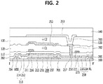
- FIG. 2 is a cross-sectional view for explaining the cross section of portion I-I' of FIG. 1
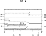
- FIG. 3 is a cross-sectional view for explaining portion II-II' of FIG. 1 .
- the organic light-emitting display device includes a plurality of pixels SP1 to SP4 arranged in a matrix form.
- Each of the pixels SP1 to SP4 includes a light-emitting area A/A having a light-emitting layer.
- the pixels SP1 to SP4 include respective pixel drive circuits, and include a plurality of lines, which transmit signals to the pixel drive circuits.
- the organic light-emitting display device may include a gate line GL for supplying a gate signal to the respective pixels SP1 to SP4, a data line DL for supplying a data signal to the respective pixels SP1 to SP4, a power line VDD for applying a power voltage VDD to the pixel drive circuit, and a reference line RL for supplying a reference voltage to the respective pixels SP1 to SP4 and sensing a voltage charged in the respective pixels SP1 to SP4, without being necessarily limited thereto.
- the pixel drive circuit includes a plurality of thin-film transistors.
- each thin-film transistor includes an active layer 200 having a channel area and first and second areas, which are configured as conductors, and a gate electrode.
- a source area is described as the first area and a drain area is described as the second area.
- the first area and the second area are not necessarily limited thereto, and the first area may be the drain area and the second area may be the source area according to the structure of the thin-film transistor.
- At least one area among the first area and the second area may be directly connected to any one of the lines.
- the active layer 200 of the thin-film transistor is configured as a conductor and is utilized as an electrode and a line so that the active layer 200 is directly connected to the other lines.
- the pixel drive circuit of the organic light-emitting display device has a 3TIC structure that includes a switching transistor 220, a driving transistor 210, a sensing transistor 230, and a storage capacitor Cst, which are disposed on a substrate 100.
- the pixel drive circuit according to the present disclosure is not necessarily limited to the above-described structure, and various other structures may be applied according to the design of the pixel drive circuit.
- a gate electrode of the switching transistor 220 may constitute a portion of the gate line GL and may be disposed along with the gate line GL.
- An input electrode 222 of the switching transistor 220 may be connected to the data line DL, and an output electrode 223 may be connected to an intermediate electrode 252 of the storage capacitor Cst.
- the input electrode may be formed by extending from the data line DL, and the output electrode may be formed by extending from the intermediate electrode of the storage capacitor Cst.
- the switching transistor 220 of the present disclosure is not necessarily limited to the above-described structure.
- the switching transistor 220 includes an active layer 221 configured to overlap the gate electrode.
- the active layer is configured such that a channel area is formed in the area thereof that overlaps the gate electrode and such that first and second areas are formed at opposite sides of the channel area so as to come into contact with the input electrode 222 and the output electrode 223 respectively.
- the first area 222 may be a source area and the second area 223 may be a drain area.
- the first area 222 may be a drain area and the second area 223 may be a source area.
- the driving transistor 210 includes a gate electrode 211 and an active layer 200.
- a channel area 216 is formed below the gate electrode 211 and a gate insulation layer 110 is located between the gate electrode 211 and the channel area 216.
- a first area 213 and a second area 218, which are configured as conductors, are located at opposite sides of the channel area 216.
- the second area 218 may be an input area that receives a drive voltage from a power line VDD
- the first area 213 may be an output area that outputs the drive voltage.
- the second area 218 extends to the top of the power line VDD.
- the second area 218 includes a first electrode portion 212, which is integrally formed with the channel area 216 and is configured as a conductor, and a first extension portion 214, which extends from the first electrode portion 212 and comes into contact with the power line VDD.
- the first extension portion 214 may come into contact with first electrode portions 212 of two neighboring pixels SP at the same time. Thereby, the first extension portion 214 supplies the drive voltage, input from the power line VDD, to the first electrode portions 212 of the two neighboring pixels SP at the same time.
- a buffer layer 261 is located between the power line and the first extension portion 214.
- the buffer layer 261 has the feature of preventing the permeation of moisture or impurities through the substrate 100.
- a portion of the power line VDD is exposed through a fourth contact hole 704.
- the first extension portion 214 comes into contact with the power line VDD through the fourth contact hole 704.
- the first area 213 may extend from the channel area 216 so as to be integrally formed with the channel area 216, and the active layer in the first area 213 may serve as a lower electrode of the storage capacitor Cst.
- the configuration of the storage capacitor Cst will be described below.
- the gate insulation layer 110 described above is located on the active layer 200, which constitutes a lower electrode 237, and an interlayer insulation layer 120 is located so as to cover the gate electrode 211.
- An intermediate electrode 252 is formed on the interlayer insulation layer 120 in the area in which the intermediate electrode 252 overlaps the lower electrode 237, and a planarization layer 130 is located so as to cover the intermediate electrode 252.
- An upper electrode 253 is located on the planarization layer 130.
- a shield layer 251 is located on the substrate 110 below the lower electrode 237 in the same layer as the power line VDD using the same material as the power line VDD, for example, a metal material.
- the buffer layer 261 is located on the power line VDD and the shield layer 251.
- the buffer layer 261 further includes a first contact hole 701, which exposes a portion of the shield layer 251.
- the lower electrode 237 is connected to the shield layer 251 through the first contact hole 710 so that the lower electrode 237 and the shield layer 251 have an equivalent potential therebetween.
- the shield layer 251 may prevent light from being introduced into a semiconductor layer 200 and may reduce parasitic capacitance generated between the lower electrode 237 and the data lines DL, thereby reducing a phenomenon of coupling between the data line DL and the gate electrode 211 of the driving transistor 210.
- the shield layer 251 of the related art has been connected to the intermediate electrode 252 through a contact hole, in the embodiment, the shield layer 251 is connected to the active layer 200, which enables a reduction in the area of the first contact hole 701, resulting in an additional increase in the aperture ratio of the pixel.
- connection electrode 217 is formed so as to come into contact with the first area 213 through the second contact hole 702.
- connection electrode 217 may be an output electrode of the driving transistor 210, for example, a source electrode, without being necessarily limited thereto.
- the connection electrode 217 is formed in the same layer as the intermediate electrode 252 of the storage capacitor Cst using the same material as the intermediate electrode 252.
- the planarization layer 130 is formed on the connection electrode 217 and the intermediate electrode 252.
- a portion of the planarization layer 130 is removed to form a third contact hole 703, which exposes the connection electrode 217.
- the upper electrode 253 is connected to the connection electrode 217 through the third contact hole 703. Thereby, the upper electrode 253 and the lower electrode 237, which are interconnected via the connection electrode 217, form an equivalent potential therebetween.
- the intermediate electrode 252 is connected to the gate electrode 211 of the driving transistor 210 through a sixth contact hole 706. Thereby, the intermediate electrode 252 is connected to both the gate electrode 211 of the driving transistor 210 and the output electrode of the switching transistor 220, thereby functioning as a node that interconnects the gate electrode 211 of the driving transistor 210, the output electrode of the switching transistor 220, and the intermediate electrode of the storage capacitor Cst.
- the active layer 200 or 221 may be formed of silicon, amorphous silicon, poly-silicon, or low-temperature poly-silicon (LTPS).
- the gate electrode 211 on the active layer 200 or the area in which no gate line GL is formed may be doped with, for example, an N-type dopant or a P-type dopant, thereby being configured as a conductor.
- the active layer 200 or 211 may be formed of a semiconductor oxide.
- the semiconductor oxide may be selected from among, for example, indium gallium zinc oxide (InGaZnO), indium tin zinc oxide (InSnZnO), indium zinc oxide (InZnO), and tin zinc oxide (SnZnO).
- the active layer 200 or 211 may be configured as a conductor via, for example, plasma processing using the gate electrode 211 and the gate line GL as a mask.
- the upper electrode 253 extends to the display area A/A so as to form a pixel electrode 301.
- the drive voltage input from the power line PL, is supplied to the pixel electrode 301 by way of the connection electrode 217 of the driving transistor 210 and the upper electrode 253.
- the upper electrode 253 functions as a node that interconnects the storage capacitor Cst, the pixel electrode 301 and the first area 213 of the driving transistor 210.
- a bank layer 140 is provided in the remaining area excluding the display area A/A, and the display area A/A is defined by the bank layer 140.
- the bank layer 140 may be formed of an organic insulation material such as, for example, poly acryl or polyimide, without being necessarily limited thereto.
- An organic layer 302 is formed on the bank layer 140 and the pixel electrode 301.
- the organic layer 302 may include a light-emitting layer in the area that corresponds to the display area A/A, and may be located on the entire surface of the bank layer 140 and the display area A/A.
- the organic layer 302 is divided into an electron injection layer (EIL), an electron transport layer (ETL), an emission layer, a hole transport layer (HTL), and a hole injection layer (HIL).
- EIL electron injection layer
- ETL electron transport layer
- HTL hole transport layer
- HIL hole injection layer
- excitons generated via recombination of electrons from a negative electrode and holes from a positive electrode return to a ground state, thereby emitting light within a specific wavelength range.
- a second electrode 303 is formed on the organic layer 302.
- the second electrode 303 may be formed on the entire surface of the substrate 100.
- the second electrode 303 may be a negative electrode.
- the first electrode 301 may be a negative electrode.
- the shield layer 251 and the intermediate electrode 252 may be formed of a single metal or an alloy thereof selected from among silver (Ag), nickel (Ni), gold (Au), platinum (Pt), aluminum (Al), copper (Cu), molybdenum (Mo), titanium (Ti), and neodymium (Nd), without being necessarily limited thereto.
- first electrode 301 and the second electrode 303 may be formed of a transparent conductive material such as, for example, indium tin oxide (ITO), indium zinc oxide (IZO), or indium gallium zinc oxide (IGZO), or a single metal or an alloy thereof among the metals that form the shield layer 251 and the intermediate electrode 252, without being necessarily limited thereto.
- a transparent conductive material such as, for example, indium tin oxide (ITO), indium zinc oxide (IZO), or indium gallium zinc oxide (IGZO), or a single metal or an alloy thereof among the metals that form the shield layer 251 and the intermediate electrode 252, without being necessarily limited thereto.
- the sensing transistor 230 includes a channel area 235, a first area 238 and a second area 232.
- a gate electrode of the sensing transistor 230 may be formed as a portion of the gate line GL, the first area may be a source area, and the second area may be a drain area, without being necessarily limited thereto.
- the first area 238 includes a second electrode portion 233, which is in contact with the channel area 235 of the sensing transistor 203 so as to be integrally formed with the channel area 235, and a second extension portion 234, which extends from the second electrode portion 233 and comes into contact with the reference line RL.
- the reference line RL may be formed in the same layer as the shield layer 251 and the power line VDD using the same material as the shield layer 251 and the power line VDD, without being necessarily limited thereto.
- the second extension portion 234 is directly connected to the reference line RL through a fifth contact hole 705 formed in the buffer layer 261.
- the second area 232 extends from the first area 213 of the driving transistor, i.e. the lower electrode 237 of the storage capacitor Cst so as to be integrally formed with the lower electrode 237.
- the first area 232 of the sensing transistor 230 serves as an input electrode, and the sensing transistor 230 does not include a separate input electrode.
- the shield layer 251, the power line VDD, and the reference line RL are formed of the same metal material.
- the respective edge portions of the shield layer 251, the power line VDD, and the reference line RL may have a tapered shape, and in other words, may be formed to have slopes.
- the driving transistor 220 and the sensing transistor 230 of the present invention has the feature that at least one of input and output electrodes, i.e. source and drain electrodes is omitted and the active layer 200, which is configured as a conductor, is in contact with the respective lines.
- the active layer 200 which is configured as a conductor, extends in a line form in order to come into contact with the respective lines, and is connected to the respective lines through contact holes.
- the organic light-emitting display device may achieve a simplified pixel structure and may reduce the generation of parasitic capacitance, which may be generated between several metals located in different layers, because lines, which have conventionally been formed using a metal of the shield layer or the source/drain electrodes, are formed using the active layer.
- lines which have conventionally been formed using a metal of the shield layer or the source/drain electrodes, are formed using the active layer.
- the lines in the pixel are formed using the active layer as described above, the number of contact holes, which are required to interconnect several lines located in different layers and the active layer, may be greatly reduced.
- the pixel drive circuit may be further densely formed owing to a great reduction in the number of contact holes.
- the area of the pixel drive circuit may be reduced in proportion to the reduction in the area of the pixel, which may secure a high aperture ratio of the pixel.
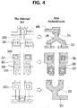
- FIG. 4 is a view illustrating variation in the structure of portions designated by dotted squares of FIG. 1 , compared to the related art.
- a drain electrode 219 is formed in the same layer as the upper electrode 253 on the drain area of the driving transistor 210 using the same metal as the upper electrode 253, and a line 2191 extending from the drain electrode 219 is connected to the top of the power line VDD through a contact hole.
- the intermediate electrode 252 extends to the area in which the connection electrode 217 is formed and is connected to the shield layer 251 thereunder through a contact hole 2192.
- the upper electrode 253 extends to form a drain electrode 2321 of the sensing transistor 230.
- a source electrode 2311 is located on the first area of the sensing transistor 231, i.e. the source area.
- the drain electrode 219 of the driving transistor 210 is omitted, and the source and drain electrodes 2311 and 2321 of the sensing transistor 230 are also omitted.
- contact holes, which are required to form the source and drain electrodes are not formed, and a contact hole 701 may be formed only in the buffer layer 261 in order to interconnect the active layer 200 and the shield layer 251.
- the area of the contact hole is greatly reduced, compared to a conventional contact hole for interconnecting the metal of the source and drain electrodes and the shield layer 251.
- the organic light-emitting display device may achieve a reduction in the number of contact holes and a great reduction in the area of some contact holes, thereby securing additional available space to enable a reduction in the area of the pixel drive circuit. That is, when the area of the pixel drive circuit is reduced, a display area of the pixel is increased, which increases the aperture ratio of the pixel.
- an organic light-emitting display device since some of lines, which have conventionally been formed using a metal material of a shield layer or source and drain electrodes, are formed using an active layer, a simplified pixel structure may be achieved and the possibility of generation of parasitic capacitance between several metals located in different layers may be reduced.
- the pixel drive circuit may be further densely formed owing to a great reduction in the number of contact holes. In this way, according to the present disclosure, the area of the pixel drive circuit may be reduced in proportion to the reduction in the area of the pixel, which may secure a high aperture ratio of the pixel.
Landscapes
- Engineering & Computer Science (AREA)
- Microelectronics & Electronic Packaging (AREA)
- Physics & Mathematics (AREA)
- Geometry (AREA)
- Electroluminescent Light Sources (AREA)
- Devices For Indicating Variable Information By Combining Individual Elements (AREA)
- Thin Film Transistor (AREA)
Abstract
Description
- The present disclosure relates to an organic light-emitting display device, and more particularly, to an organic light-emitting display device, which may increase the aperture ratio of each pixel by using a semiconductor pattern of a thin-film transistor array as a line.
- An image display device, which realizes various pieces of information on a screen, is a core technology of the information and communication age, and is being developed in the direction of becoming thinner, lighter, more portable, and having higher performance. In response, as a flat panel display device that is thinner and lighter than a cathode ray tube (CRT), for example, an organic light-emitting display device, which controls the amount of light emitted from an organic light-emitting layer to display an image, is in the spotlight.
- In an organic light-emitting display device, a plurality of pixels is arranged in a matrix form to display an image. Here, each pixel includes a light-emitting element, and a pixel drive circuit including, for example, a plurality of transistors and storage capacitors to independently drive the light-emitting element.
- Recently, since the area of individual pixels is reduced with an improvement in the resolution of the organic light-emitting display device, in order to minimize a reduction in the aperture ratio of each pixel due to the reduced area of the pixel, the area of each pixel drive circuit also needs to be reduced. However, when the area of the pixel drive circuit is reduced, distances between respective lines, transistors, and storage capacitors are reduced, causing parasitic capacitance between components of the pixel drive circuit, which may cause coupling of multiple signals, or a short-circuit phenomenon in which the lines become interconnected. Thereby, there is a limitation to the extent to which the area of the pixel drive circuit can be reduced.
- In particular, in an organic light-emitting display device of the related art, respective electrodes of storage capacitors and thin-film transistors of each pixel drive circuit are connected to a shield layer, which is a lower layer on a substrate, and metal lines, which are formed in the same layer as source and drain electrodes of the thin-film transistor, which is an upper layer on the substrate, through contact holes. Accordingly, since the organic light-emitting display device of the related art requires a predetermined number or more of contact holes according to the structure of the pixel drive circuit, and has a limitation on the extent to which the area of each contact hole can be reduced in order to prevent the parasitic capacitance and short-circuit mentioned above, the extent to which the area of the pixel drive circuit can be reduced is consequently limited due to the presence of the contact holes.
- Due to the problems described above, in a high-resolution organic light-emitting display device, when the area of the pixel drive circuit is not sufficiently reduced in proportion to the reduction in the area of the pixel, the aperture ratio of each pixel may be reduced, causing a reduction in the brightness and luminous efficacy of the organic light-emitting display device.
- Accordingly, the present disclosure is directed to an organic light-emitting display device that substantially addresses one or more problems due to limitations and disadvantages of the related art.
- An object of the present disclosure is to provide an organic light-emitting display device, which may reduce the area of a pixel drive circuit and increase the aperture ratio of a pixel by forming lines inside the pixel using a semiconductor pattern that forms a channel of each thin-film transistor array.
- Additional advantages, objects, and features of the invention will be set forth in part in the description which follows and in part will become apparent to those having ordinary skill in the art upon examination of the following. The objectives and other advantages may be realized and attained by the structure particularly pointed out in the written description and claims hereof as well as the appended drawings.
- To achieve these objects and other advantages, as embodied and described herein, an organic light-emitting display device includes a plurality of pixels and a plurality of lines configured to drive the pixels, wherein each pixel includes a thin-film transistor including an active layer having a first area and a second area, which are configured as conductors, and a gate electrode. Here, at least one of the first area and the second area of the thin-film transistor is directly connected to a corresponding line among the lines.
- An area connected to the line includes an electrode portion integrally formed with a channel area of the thin-film transistor and an extension portion configured to extend from the electrode portion to a top of the line so as to be directly connected to the line.
- It is to be understood that both the foregoing general description and the following detailed description are exemplary and explanatory.
- The accompanying drawings, which are included to provide a further understanding of the disclosure and are incorporated in and constitute a part of this application, illustrate embodiment(s) and together with the description serve to explain the principle of the disclosure.
-
FIG. 1 is a plan view for explaining a pixel structure of an organic light-emitting display device according to one embodiment. -
FIG. 2 is a cross-sectional view for explaining the cross section of portion I-I' ofFIG. 1 . -
FIG. 3 is a cross-sectional view for explaining portion II-II' ofFIG. 1 ; and -
FIG. 4 is a view illustrating variation in the structure of portions designated by dotted squares ofFIG. 1 , compared to the related art. - Hereinafter, exemplary embodiments will be described with reference to the accompanying drawings. In the entire specification, the same or similar elements are denoted by the same reference numerals even though they are depicted in different drawings. In the following description, a detailed description of known functions and configurations incorporated herein will be omitted when it may make the subject matter unclear. Also, the terms used in the following description are terms defined taking into consideration the functions obtained in accordance with the present disclosure, and may differ from the names of parts of actual products.
- In the case of a description with respect to positional relations, when an element is referred to as being, for example, "on", "above", "under", and "aside" another element, it may be directly on the other element or intervening elements may also be present.
- Although terms such as, for example, "first" and "second" are used to describe various components, these components are not limited by these terms. These terms are merely used to distinguish any one component from another component. Thus, "a first component" mentioned below may be "a second component" within the technical sprit of the present invention.
- In the drawings, the thickness and size of each component are illustrated for convenience of description, and the present disclosure is not necessary to be limited to the size and thickness of the illustrated component.
- Hereinafter, various embodiments will be described in detail with reference to the accompanying drawings.
-
FIG. 1 is a plan view for explaining a pixel structure of an organic light-emitting display device according to one embodiment, andFIG. 2 is a cross-sectional view for explaining the cross section of portion I-I' ofFIG. 1 . In addition,FIG. 3 is a cross-sectional view for explaining portion II-II' ofFIG. 1 . - The organic light-emitting display device includes a plurality of pixels SP1 to SP4 arranged in a matrix form. Each of the pixels SP1 to SP4 includes a light-emitting area A/A having a light-emitting layer. In addition, the pixels SP1 to SP4 include respective pixel drive circuits, and include a plurality of lines, which transmit signals to the pixel drive circuits. For example, the organic light-emitting display device according to an embodiment of the present invention may include a gate line GL for supplying a gate signal to the respective pixels SP1 to SP4, a data line DL for supplying a data signal to the respective pixels SP1 to SP4, a power line VDD for applying a power voltage VDD to the pixel drive circuit, and a reference line RL for supplying a reference voltage to the respective pixels SP1 to SP4 and sensing a voltage charged in the respective pixels SP1 to SP4, without being necessarily limited thereto.
- The pixel drive circuit includes a plurality of thin-film transistors. Here, each thin-film transistor includes an
active layer 200 having a channel area and first and second areas, which are configured as conductors, and a gate electrode. In the present embodiment, for convenience, a source area is described as the first area and a drain area is described as the second area. However, the first area and the second area are not necessarily limited thereto, and the first area may be the drain area and the second area may be the source area according to the structure of the thin-film transistor. - In at least one of the thin-film transistors, at least one area among the first area and the second area may be directly connected to any one of the lines. In other words, instead of forming source and drain electrodes on the first area and the second area, the
active layer 200 of the thin-film transistor is configured as a conductor and is utilized as an electrode and a line so that theactive layer 200 is directly connected to the other lines. - The feature described above will be described below in detail with reference to the embodiment of
FIGs. 1 to 3 . The pixel drive circuit of the organic light-emitting display device according to the embodiment ofFIGs. 1 to 3 has a 3TIC structure that includes aswitching transistor 220, adriving transistor 210, asensing transistor 230, and a storage capacitor Cst, which are disposed on asubstrate 100. However, the pixel drive circuit according to the present disclosure is not necessarily limited to the above-described structure, and various other structures may be applied according to the design of the pixel drive circuit. - A gate electrode of the
switching transistor 220 may constitute a portion of the gate line GL and may be disposed along with the gate line GL. Aninput electrode 222 of theswitching transistor 220 may be connected to the data line DL, and anoutput electrode 223 may be connected to anintermediate electrode 252 of the storage capacitor Cst. Here, the input electrode may be formed by extending from the data line DL, and the output electrode may be formed by extending from the intermediate electrode of the storage capacitor Cst. However, theswitching transistor 220 of the present disclosure is not necessarily limited to the above-described structure. - The
switching transistor 220 includes anactive layer 221 configured to overlap the gate electrode. The active layer is configured such that a channel area is formed in the area thereof that overlaps the gate electrode and such that first and second areas are formed at opposite sides of the channel area so as to come into contact with theinput electrode 222 and theoutput electrode 223 respectively. - In an N-type transistor, the
first area 222 may be a source area and thesecond area 223 may be a drain area. In a P-type transistor, thefirst area 222 may be a drain area and thesecond area 223 may be a source area. - Referring to
FIGs. 2 and3 , thedriving transistor 210 includes agate electrode 211 and anactive layer 200. Explaining theactive layer 200 in more detail, achannel area 216 is formed below thegate electrode 211 and agate insulation layer 110 is located between thegate electrode 211 and thechannel area 216. In addition, afirst area 213 and asecond area 218, which are configured as conductors, are located at opposite sides of thechannel area 216. Here, thesecond area 218 may be an input area that receives a drive voltage from a power line VDD, and thefirst area 213 may be an output area that outputs the drive voltage. - Referring to
FIG. 2 , thesecond area 218 extends to the top of the power line VDD. Here, thesecond area 218 includes afirst electrode portion 212, which is integrally formed with thechannel area 216 and is configured as a conductor, and afirst extension portion 214, which extends from thefirst electrode portion 212 and comes into contact with the power line VDD. Here, thefirst extension portion 214 may come into contact withfirst electrode portions 212 of two neighboring pixels SP at the same time. Thereby, thefirst extension portion 214 supplies the drive voltage, input from the power line VDD, to thefirst electrode portions 212 of the two neighboring pixels SP at the same time. - A
buffer layer 261 is located between the power line and thefirst extension portion 214. Thebuffer layer 261 has the feature of preventing the permeation of moisture or impurities through thesubstrate 100. - A portion of the power line VDD is exposed through a
fourth contact hole 704. Thefirst extension portion 214 comes into contact with the power line VDD through thefourth contact hole 704. - The
first area 213 may extend from thechannel area 216 so as to be integrally formed with thechannel area 216, and the active layer in thefirst area 213 may serve as a lower electrode of the storage capacitor Cst. - The configuration of the storage capacitor Cst will be described below. The
gate insulation layer 110 described above is located on theactive layer 200, which constitutes alower electrode 237, and aninterlayer insulation layer 120 is located so as to cover thegate electrode 211. Anintermediate electrode 252 is formed on theinterlayer insulation layer 120 in the area in which theintermediate electrode 252 overlaps thelower electrode 237, and aplanarization layer 130 is located so as to cover theintermediate electrode 252. Anupper electrode 253 is located on theplanarization layer 130. In this way, the storage capacitor Cst, which includes double capacitors between thelower electrode 237 and theintermediate electrode 252 and between theintermediate electrode 252 and theupper electrode 253, is provided. Here, ashield layer 251 is located on thesubstrate 110 below thelower electrode 237 in the same layer as the power line VDD using the same material as the power line VDD, for example, a metal material. As mentioned above, thebuffer layer 261 is located on the power line VDD and theshield layer 251. Thebuffer layer 261 further includes afirst contact hole 701, which exposes a portion of theshield layer 251. Thelower electrode 237 is connected to theshield layer 251 through the first contact hole 710 so that thelower electrode 237 and theshield layer 251 have an equivalent potential therebetween. - The
shield layer 251 may prevent light from being introduced into asemiconductor layer 200 and may reduce parasitic capacitance generated between thelower electrode 237 and the data lines DL, thereby reducing a phenomenon of coupling between the data line DL and thegate electrode 211 of the drivingtransistor 210. Although theshield layer 251 of the related art has been connected to theintermediate electrode 252 through a contact hole, in the embodiment, theshield layer 251 is connected to theactive layer 200, which enables a reduction in the area of thefirst contact hole 701, resulting in an additional increase in the aperture ratio of the pixel. - A portion of the
interlayer insulation layer 120 and thegate insulation layer 110 is removed in the area that corresponds to thelower electrode 237, i.e. the edge of thefirst area 213 of theactive layer 200 so as to form asecond contact hole 702, which exposes a portion of thefirst area 213. Aconnection electrode 217 is formed so as to come into contact with thefirst area 213 through thesecond contact hole 702. Here, theconnection electrode 217 may be an output electrode of the drivingtransistor 210, for example, a source electrode, without being necessarily limited thereto. Theconnection electrode 217 is formed in the same layer as theintermediate electrode 252 of the storage capacitor Cst using the same material as theintermediate electrode 252. Theplanarization layer 130 is formed on theconnection electrode 217 and theintermediate electrode 252. A portion of theplanarization layer 130 is removed to form athird contact hole 703, which exposes theconnection electrode 217. Theupper electrode 253 is connected to theconnection electrode 217 through thethird contact hole 703. Thereby, theupper electrode 253 and thelower electrode 237, which are interconnected via theconnection electrode 217, form an equivalent potential therebetween. - Meanwhile, referring to
FIG. 3 , theintermediate electrode 252 is connected to thegate electrode 211 of the drivingtransistor 210 through asixth contact hole 706. Thereby, theintermediate electrode 252 is connected to both thegate electrode 211 of the drivingtransistor 210 and the output electrode of the switchingtransistor 220, thereby functioning as a node that interconnects thegate electrode 211 of the drivingtransistor 210, the output electrode of the switchingtransistor 220, and the intermediate electrode of the storage capacitor Cst. - Here, the
active layer gate electrode 211 on theactive layer 200 or the area in which no gate line GL is formed may be doped with, for example, an N-type dopant or a P-type dopant, thereby being configured as a conductor. - In addition, the
active layer active layer gate electrode 211 and the gate line GL as a mask. - Referring to
FIGs. 1 and3 , theupper electrode 253 extends to the display area A/A so as to form apixel electrode 301. Here, the drive voltage, input from the power line PL, is supplied to thepixel electrode 301 by way of theconnection electrode 217 of the drivingtransistor 210 and theupper electrode 253. In other words, theupper electrode 253 functions as a node that interconnects the storage capacitor Cst, thepixel electrode 301 and thefirst area 213 of the drivingtransistor 210. - Here, a
bank layer 140 is provided in the remaining area excluding the display area A/A, and the display area A/A is defined by thebank layer 140. - The
bank layer 140 may be formed of an organic insulation material such as, for example, poly acryl or polyimide, without being necessarily limited thereto. - An
organic layer 302 is formed on thebank layer 140 and thepixel electrode 301. Theorganic layer 302 may include a light-emitting layer in the area that corresponds to the display area A/A, and may be located on the entire surface of thebank layer 140 and the display area A/A. - Here, the
organic layer 302 is divided into an electron injection layer (EIL), an electron transport layer (ETL), an emission layer, a hole transport layer (HTL), and a hole injection layer (HIL). In the light-emitting layer, excitons generated via recombination of electrons from a negative electrode and holes from a positive electrode return to a ground state, thereby emitting light within a specific wavelength range. - A
second electrode 303 is formed on theorganic layer 302. Thesecond electrode 303 may be formed on the entire surface of thesubstrate 100. - Here, when the
first electrode 301 is a positive electrode, thesecond electrode 303 may be a negative electrode. Alternatively, when thesecond electrode 303 is a positive electrode, thefirst electrode 301 may be a negative electrode. - The
shield layer 251 and theintermediate electrode 252 may be formed of a single metal or an alloy thereof selected from among silver (Ag), nickel (Ni), gold (Au), platinum (Pt), aluminum (Al), copper (Cu), molybdenum (Mo), titanium (Ti), and neodymium (Nd), without being necessarily limited thereto. - In addition, the
first electrode 301 and thesecond electrode 303 may be formed of a transparent conductive material such as, for example, indium tin oxide (ITO), indium zinc oxide (IZO), or indium gallium zinc oxide (IGZO), or a single metal or an alloy thereof among the metals that form theshield layer 251 and theintermediate electrode 252, without being necessarily limited thereto. - The
sensing transistor 230 includes achannel area 235, afirst area 238 and asecond area 232. A gate electrode of thesensing transistor 230 may be formed as a portion of the gate line GL, the first area may be a source area, and the second area may be a drain area, without being necessarily limited thereto. - The
first area 238 includes asecond electrode portion 233, which is in contact with thechannel area 235 of the sensing transistor 203 so as to be integrally formed with thechannel area 235, and asecond extension portion 234, which extends from thesecond electrode portion 233 and comes into contact with the reference line RL. The reference line RL may be formed in the same layer as theshield layer 251 and the power line VDD using the same material as theshield layer 251 and the power line VDD, without being necessarily limited thereto. Thesecond extension portion 234 is directly connected to the reference line RL through afifth contact hole 705 formed in thebuffer layer 261. - The
second area 232 extends from thefirst area 213 of the driving transistor, i.e. thelower electrode 237 of the storage capacitor Cst so as to be integrally formed with thelower electrode 237. Here, thefirst area 232 of thesensing transistor 230 serves as an input electrode, and thesensing transistor 230 does not include a separate input electrode. - The
shield layer 251, the power line VDD, and the reference line RL are formed of the same metal material. Here, when edge portions of these components are vertically formed, there is a possibility of disconnection of theactive layer 200 located thereon. Therefore, in order to prevent disconnection of theactive layer 200, the respective edge portions of theshield layer 251, the power line VDD, and the reference line RL may have a tapered shape, and in other words, may be formed to have slopes. - As described above, the driving
transistor 220 and thesensing transistor 230 of the present invention has the feature that at least one of input and output electrodes, i.e. source and drain electrodes is omitted and theactive layer 200, which is configured as a conductor, is in contact with the respective lines. To this end, theactive layer 200, which is configured as a conductor, extends in a line form in order to come into contact with the respective lines, and is connected to the respective lines through contact holes. - Accordingly, the organic light-emitting display device according to the present invention may achieve a simplified pixel structure and may reduce the generation of parasitic capacitance, which may be generated between several metals located in different layers, because lines, which have conventionally been formed using a metal of the shield layer or the source/drain electrodes, are formed using the active layer. In addition, when the lines in the pixel are formed using the active layer as described above, the number of contact holes, which are required to interconnect several lines located in different layers and the active layer, may be greatly reduced. Therefore, although a reduction in the area of the pixel drive circuit has conventionally been limited due to a large number of contact holes even if the area of each pixel is reduced, according to the present disclosure, the pixel drive circuit may be further densely formed owing to a great reduction in the number of contact holes. In this way, according to the present disclosure, the area of the pixel drive circuit may be reduced in proportion to the reduction in the area of the pixel, which may secure a high aperture ratio of the pixel.
-
FIG. 4 is a view illustrating variation in the structure of portions designated by dotted squares ofFIG. 1 , compared to the related art. - In the related art, a
drain electrode 219 is formed in the same layer as theupper electrode 253 on the drain area of the drivingtransistor 210 using the same metal as theupper electrode 253, and aline 2191 extending from thedrain electrode 219 is connected to the top of the power line VDD through a contact hole. - In addition, the
intermediate electrode 252 extends to the area in which theconnection electrode 217 is formed and is connected to theshield layer 251 thereunder through acontact hole 2192. Theupper electrode 253 extends to form adrain electrode 2321 of thesensing transistor 230. Meanwhile, asource electrode 2311 is located on the first area of thesensing transistor 231, i.e. the source area. - On the other hand, according to one embodiment, since no line extends from the
upper electrode 252 and theactive layer 200 forms a line, thedrain electrode 219 of the drivingtransistor 210 is omitted, and the source anddrain electrodes sensing transistor 230 are also omitted. Thereby, contact holes, which are required to form the source and drain electrodes, are not formed, and acontact hole 701 may be formed only in thebuffer layer 261 in order to interconnect theactive layer 200 and theshield layer 251. In this case, the area of the contact hole is greatly reduced, compared to a conventional contact hole for interconnecting the metal of the source and drain electrodes and theshield layer 251. - As described above, the organic light-emitting display device according to one embodiment may achieve a reduction in the number of contact holes and a great reduction in the area of some contact holes, thereby securing additional available space to enable a reduction in the area of the pixel drive circuit. That is, when the area of the pixel drive circuit is reduced, a display area of the pixel is increased, which increases the aperture ratio of the pixel.
- As is apparent from the above description, in an organic light-emitting display device according to one embodiment, since some of lines, which have conventionally been formed using a metal material of a shield layer or source and drain electrodes, are formed using an active layer, a simplified pixel structure may be achieved and the possibility of generation of parasitic capacitance between several metals located in different layers may be reduced.
- In addition, when the lines in a pixel are formed using the active layer, the number of contact holes, which are required to interconnect several lines located in different layers and the active layer, may be greatly reduced. Therefore, although a reduction in the area of the pixel drive circuit has conventionally been limited due to a large number of contact holes even if the area of each pixel is reduced, according to the present disclosure, the pixel drive circuit may be further densely formed owing to a great reduction in the number of contact holes. In this way, according to the present disclosure, the area of the pixel drive circuit may be reduced in proportion to the reduction in the area of the pixel, which may secure a high aperture ratio of the pixel.
- Although the embodiments have been described above in detail with reference to the accompanying drawings, it will be apparent to those skilled in the art that the present disclosure is not limited to the embodiments described above, and various substitutions, modifications, and alterations may be devised within the scope of the disclosure. Accordingly, various embodiments are not intended to limit the present disclosure, and the scope of the disclosure is not limited by the embodiments. Accordingly, the disclosed embodiments are provided for the purpose of description and are not intended to limit the technical scope of the disclosure, and the technical scope of the disclosure is not limited by the embodiments. The range of the disclosure should be interpreted based on the following claims.
- Further embodiments are defined in the following numbered clauses:
- 1. An organic light-emitting display device comprising a plurality of pixels arranged in a matrix form and a plurality of lines configured to supply a signal for driving each pixel, wherein each pixel includes a thin-film transistor including an active layer having a first area and a second area, which are configured as conductors, and a gate electrode, and wherein at least one of the first area and the second area is directly connected to a corresponding line among the lines.
- 2. The device according to clause 1, wherein the area directly connected to the line, among the first and second areas, includes an electrode portion integrally formed with a channel area of the thin-film transistor and an extension portion configured to extend from the electrode portion so as to be directly connected to the line.
- 3. The device according to clause 1, wherein each pixel further includes a capacitor, and wherein the capacitor includes: a shield layer located on a substrate; a lower electrode configured to overlap the shield layer with a buffer layer interposed therebetween, the lower electrode being connected to the shield layer through a first contact hole and being formed of the active layer, which is configured as a conductor; an intermediate electrode configured to overlap the active layer with a gate insulation layer and an interlayer insulation layer interposed therebetween; and an upper electrode configured to overlap the intermediate electrode with a passivation layer interposed therebetween.
- 4. The device according to clause 1, wherein one of the thin-film transistors is a driving transistor, and wherein the driving transistor further includes a connection electrode configured to come into contact with the first area through a second contact hole, the connection electrode is connected to a pixel electrode through a third contact hole, and the second area is directly connected to a power line, which supplies a drive voltage to the pixel and is arranged in a vertical direction, among the lines through a fourth contact hole.
- 5. The device according to clause 4, wherein the second area of the driving transistor includes a first electrode portion integrally formed with a channel area of the driving transistor and a first extension portion configured to extend from the first electrode portion so as to be connected to the power line.
- 6. The device according to clause 5, wherein the first electrode portion extends from the channel area and is connected to the first electrode portion of the driving transistor of another neighboring pixel, and the first extension portion extends from a point at which the first electrode portions of two neighboring pixels are connected to each other and is connected to the power line.
- 7. The device according to clause 1, wherein one of the thin-film transistors is a sensing transistor, and wherein the first area of the sensing transistor is directly connected to a reference line, which supplies a reference voltage to the pixel and senses a voltage charted in the pixel, among the lines through a fifth contact hole, and wherein the second area of the sensing transistor extends from the first area of the driving transistor and is integrally formed with the first area.
- 8. The device according to clause 7, wherein the first area of the sensing transistor includes a second electrode portion configured to come into contact with a channel area of the sensing transistor so as to be integrally formed with the channel area and a second extension portion configured to extend from the second electrode portion so as to be connected to the reference line, which is arranged in a vertical direction, through the fifth contact hole.
- 9. The device according to clause 8, wherein the second electrode portion comes into contact with the second electrode portion of the sensing transistor provided in a neighboring pixel, and wherein the second extension portion extends from a point at which the second electrode portions of two neighboring sensing transistors are connected to each other and is directly connected to the reference line through the fifth contact hole.
- 10. The device according to clause 3, wherein the shield layer is formed in the same layer as a power line, which supplies a drive voltage to each pixel, and a reference line, which supplies a reference voltage to the pixel and senses a voltage charged in the pixel, among the lines, using the same material as the power line and the reference line.
- 11. The device according to clause 7, wherein the gate electrode of the sensing transistor is connected to a gate line, which supplies a gate signal to each pixel, among the lines.
- 12. The device according to clause 10, wherein the shield layer, the reference line and the power line include edge portions each having a tapered shape.
Claims (12)
- An organic light-emitting display device comprising a plurality of pixels arranged in a matrix form and a plurality of lines each configured to supply a signal for driving each pixel,
wherein each pixel includes a thin-film transistor including an active layer having a first area (222) and a second area (223), which are configured as conductors, and a gate electrode, and
wherein at least one of the first area and the second area is directly connected to a corresponding line among the plurality of lines. - The device according to claim 1, wherein the area directly connected to the corresponding line, among the first and second areas, includes an electrode portion (212, 233) integrally formed with a channel area (235) of the thin-film transistor and an extension portion (214, 234) configured to extend from the electrode portion so as to be directly connected to the corresponding line.
- The device according to claim 1 or 2, wherein each pixel further includes a capacitor (Cst), and
wherein the capacitor includes:a shield layer (251) located on a substrate (100);a lower electrode (237) configured to overlap the shield layer with a buffer layer (261) interposed therebetween, the lower electrode being connected to the shield layer through a first contact hole (701) and being formed of the active layer, which is configured as a conductor;an intermediate electrode (252) configured to overlap the active layer with a gate insulation layer (110) and an interlayer insulation layer (120) interposed therebetween; andan upper electrode (253) configured to overlap the intermediate electrode with a planarization layer 130 interposed therebetween. - The device according to any previous claim, wherein the thin-film transistor is a driving transistor (210), and
wherein the driving transistor further includes a connection electrode (217) configured to come into contact with the first area through a second contact hole (702), the connection electrode is connected to a pixel electrode (301) through a third contact hole (703), and the second area is directly connected to a power line (VDD), which supplies a drive voltage to the pixel and is arranged in a vertical direction, among the plurality of lines through a fourth contact hole (704) . - The device according to claim 4, wherein the second area of the driving transistor includes a first electrode portion (212) integrally formed with a channel area of the driving transistor and a first extension portion (214) configured to extend from the first electrode portion so as to be connected to the power line (VDD).
- The device according to claim 5, wherein the first electrode portion of a first pixel of the plurality of pixels extends from the channel area of the first pixel and is connected to the first electrode portion of the driving transistor of a second pixel of the plurality of pixels, the second pixel neighboring the first pixel, wherein the first extension portion of the first pixel extends from a point at which the first electrode portion of the first pixel connects to the first extension portion of the second pixel and is connected to the power line.
- The device according to any of claims 1 to 3, wherein the thin-film transistor is a sensing transistor (230), and
wherein the first area of the sensing transistor is directly connected to a reference line (RL), which supplies a reference voltage to the pixel and senses a voltage charted in the pixel, among the plurality of lines through a fifth contact hole (705), and
wherein the second area of the sensing transistor extends from the first area of the driving transistor and is integrally formed with the first area. - The device according to claim 7, wherein the first area of the sensing transistor includes a second electrode portion (233) configured to come into contact with a channel area (235) of the sensing transistor so as to be integrally formed with the channel area and a second extension portion (234) configured to extend from the second electrode portion so as to be connected to the reference line, which is arranged in a vertical direction, through the fifth contact hole.
- The device according to claim 8, wherein the second electrode portion of a first pixel of the plurality of pixels comes into contact with the second electrode portion of the sensing transistor of a second pixel of the plurality of pixels, the first pixel neighboring the second pixel, and
wherein the second extension portion of the first pixel extends from a point at which the second electrode portions of the first and second pixels are connected to each other and is directly connected to the reference line through the fifth contact hole. - The device according to claim 3, wherein the shield layer is formed in the same layer as a power line, which supplies a drive voltage to each pixel, and a reference line, which supplies a reference voltage to the pixel and senses a voltage charged in the pixel, among the plurality of lines, using the same material as the power line and the reference line.
- The device according to any of claims 7 to 10, wherein the gate electrode of the sensing transistor is connected to a gate line, which supplies a gate signal to each pixel, among the plurality of lines.
- The device according to claim 10 or 11, wherein the shield layer, the reference line and the power line include edge portions each having a tapered shape.
Applications Claiming Priority (1)
| Application Number | Priority Date | Filing Date | Title |
|---|---|---|---|
| KR1020160143719A KR102824654B1 (en) | 2016-10-31 | 2016-10-31 | Organic light emitting diode display |
Publications (2)
| Publication Number | Publication Date |
|---|---|
| EP3316309A1 true EP3316309A1 (en) | 2018-05-02 |
| EP3316309B1 EP3316309B1 (en) | 2022-01-26 |
Family
ID=60182390
Family Applications (1)
| Application Number | Title | Priority Date | Filing Date |
|---|---|---|---|
| EP17197796.0A Active EP3316309B1 (en) | 2016-10-31 | 2017-10-23 | Organic light-emitting display device |
Country Status (6)
| Country | Link |
|---|---|
| US (1) | US10468477B2 (en) |
| EP (1) | EP3316309B1 (en) |
| JP (1) | JP6458103B2 (en) |
| KR (1) | KR102824654B1 (en) |
| CN (1) | CN108022946B (en) |
| TW (1) | TWI636447B (en) |
Families Citing this family (27)
| Publication number | Priority date | Publication date | Assignee | Title |
|---|---|---|---|---|
| KR102668224B1 (en) * | 2016-11-30 | 2024-05-24 | 엘지디스플레이 주식회사 | Display Device |
| CN207909879U (en) * | 2018-03-28 | 2018-09-25 | 京东方科技集团股份有限公司 | array substrate, display panel and display device |
| CN109037297B (en) * | 2018-08-09 | 2021-01-29 | 京东方科技集团股份有限公司 | An organic light-emitting display substrate and a manufacturing method thereof |
| KR102709997B1 (en) | 2018-09-18 | 2024-09-26 | 엘지디스플레이 주식회사 | Organic light emitting display device |
| KR102652769B1 (en) | 2018-10-01 | 2024-04-02 | 삼성디스플레이 주식회사 | Display device and fabricating method thereof |
| KR102593534B1 (en) | 2018-10-10 | 2023-10-25 | 삼성디스플레이 주식회사 | Display apparatus |
| KR102698949B1 (en) * | 2018-11-28 | 2024-08-26 | 삼성디스플레이 주식회사 | Organic light emitting diode display device |
| KR102638207B1 (en) * | 2018-12-21 | 2024-02-16 | 엘지디스플레이 주식회사 | Display device |
| KR102648420B1 (en) * | 2018-12-28 | 2024-03-18 | 엘지디스플레이 주식회사 | Display apparatus including a unit pixel composed of four sub-pixels |
| KR102783427B1 (en) | 2019-01-18 | 2025-03-18 | 삼성디스플레이 주식회사 | Display device |
| CN110299384B (en) * | 2019-06-10 | 2021-09-07 | 昆山国显光电有限公司 | a display panel |
| KR102895955B1 (en) | 2019-06-14 | 2025-12-04 | 삼성디스플레이 주식회사 | Display apparatus and Method for manufacturing the same |
| CN110335564A (en) * | 2019-06-29 | 2019-10-15 | 上海天马有机发光显示技术有限公司 | A kind of array substrate, display panel and display device |
| KR102791404B1 (en) * | 2019-12-20 | 2025-04-08 | 엘지디스플레이 주식회사 | Thin film transistor array substrate and electronic device including the same |
| EP3846216B1 (en) * | 2019-12-30 | 2024-09-25 | LG Display Co., Ltd. | Display panel and repair method thereof |
| KR20210086441A (en) | 2019-12-30 | 2021-07-08 | 엘지디스플레이 주식회사 | Display panel and repair method thereof |
| US11985871B2 (en) * | 2019-12-31 | 2024-05-14 | Lg Display Co., Ltd. | Display device and method of manufacturing same |
| CN111326558B (en) * | 2020-02-27 | 2023-11-28 | 合肥京东方卓印科技有限公司 | Display panels and electronic devices |
| US11925067B2 (en) | 2020-05-11 | 2024-03-05 | Boe Technology Group Co., Ltd. | Display panel and display device |
| KR102955847B1 (en) * | 2020-09-01 | 2026-04-21 | 엘지디스플레이 주식회사 | Organic light emitting diode display device and its manufacturing method |
| KR102698618B1 (en) | 2020-10-20 | 2024-08-27 | 엘지디스플레이 주식회사 | Thin film transistor array substrate and electronic device including the same |
| CN113516947B (en) * | 2021-04-22 | 2023-01-17 | 武汉天马微电子有限公司 | Display panel and display device |
| KR102862546B1 (en) | 2021-05-03 | 2025-09-22 | 삼성디스플레이 주식회사 | Display device |
| CN113871427B (en) | 2021-09-14 | 2023-06-02 | 武汉华星光电半导体显示技术有限公司 | Display panel and electronic equipment |
| JP7642818B2 (en) * | 2022-01-26 | 2025-03-10 | 恵科股▲分▼有限公司 | Array substrate and liquid crystal display panel |
| CN114530458B (en) * | 2022-01-27 | 2022-11-29 | 长沙惠科光电有限公司 | Display panel and method for manufacturing display panel |
| CN114609813B (en) * | 2022-03-22 | 2023-07-25 | 深圳市华星光电半导体显示技术有限公司 | Array substrate and liquid crystal display panel |
Citations (4)
| Publication number | Priority date | Publication date | Assignee | Title |
|---|---|---|---|---|
| US20070069205A1 (en) * | 2005-09-26 | 2007-03-29 | Sanyo Electric Co., Ltd. | Organic electroluminescent display device |
| US20090295773A1 (en) * | 2008-05-29 | 2009-12-03 | Sony Corporation | Display device |
| US20160005804A1 (en) * | 2014-07-04 | 2016-01-07 | Lg Display Co., Ltd. | Organic light emitting display and method of fabricating the same |
| EP3029733A1 (en) * | 2014-12-06 | 2016-06-08 | LG Display Co., Ltd. | Organic light emitting display device |
Family Cites Families (21)
| Publication number | Priority date | Publication date | Assignee | Title |
|---|---|---|---|---|
| JP3744227B2 (en) * | 1998-09-24 | 2006-02-08 | セイコーエプソン株式会社 | ELECTRO-OPTICAL DEVICE, MANUFACTURING METHOD THEREOF, AND ELECTRONIC DEVICE |
| JP4666710B2 (en) * | 1999-01-21 | 2011-04-06 | 株式会社半導体エネルギー研究所 | Semiconductor device and manufacturing method thereof |
| TW507258B (en) * | 2000-02-29 | 2002-10-21 | Semiconductor Systems Corp | Display device and method for fabricating the same |
| KR100892945B1 (en) * | 2002-02-22 | 2009-04-09 | 삼성전자주식회사 | Active matrix organic light emitting display device and manufacturing method thereof |
| TWI570691B (en) | 2006-04-05 | 2017-02-11 | 半導體能源研究所股份有限公司 | Semiconductor device, display device, and electronic device |
| KR20130089044A (en) | 2012-02-01 | 2013-08-09 | 삼성디스플레이 주식회사 | Semiconductor device and flat panel display device having the same |
| JP6015389B2 (en) | 2012-11-30 | 2016-10-26 | 株式会社リコー | Field effect transistor, display element, image display device, and system |
| US9673267B2 (en) * | 2013-03-26 | 2017-06-06 | Lg Display Co., Ltd. | Organic light emitting diode display device having a capacitor with stacked storage electrodes and method for manufacturing the same |
| KR101548304B1 (en) * | 2013-04-23 | 2015-08-28 | 엘지디스플레이 주식회사 | Organic Light Emitting Diode Display Device and Method for Manufacturing The Same |
| US20150013709A1 (en) * | 2013-07-12 | 2015-01-15 | Chris Scheurn | Devices And Methods For Contacting Keratinaceous Nails With Solutions |
| KR20150054210A (en) * | 2013-11-11 | 2015-05-20 | 삼성디스플레이 주식회사 | Organic light emitting diode display |
| KR102049793B1 (en) * | 2013-11-15 | 2020-01-08 | 엘지디스플레이 주식회사 | Organic light emitting display device |
| KR102189223B1 (en) * | 2014-07-10 | 2020-12-10 | 삼성디스플레이 주식회사 | Organic light emitting display, driving method thereof and manufacturing method thereof |
| KR102184904B1 (en) * | 2014-08-28 | 2020-12-02 | 엘지디스플레이 주식회사 | Organic light emitting display panel and display device |
| KR102326313B1 (en) * | 2014-11-20 | 2021-11-15 | 삼성디스플레이 주식회사 | Organic light emitting diode display device |
| KR102463886B1 (en) * | 2015-01-16 | 2022-11-07 | 삼성디스플레이 주식회사 | Display apparatus and manufacturing method thereof |
| KR102422108B1 (en) * | 2015-01-20 | 2022-07-19 | 삼성디스플레이 주식회사 | Organic light emitting diode display |
| KR102415753B1 (en) * | 2015-05-04 | 2022-07-01 | 삼성디스플레이 주식회사 | Organic light emitting diode display |
| KR102571085B1 (en) * | 2016-04-04 | 2023-08-28 | 삼성디스플레이 주식회사 | Display device |
| KR102543577B1 (en) * | 2016-04-07 | 2023-06-14 | 삼성디스플레이 주식회사 | Transistor array panel, manufacturing method thereof, and disalay device comprising the same |
| KR102567715B1 (en) * | 2016-04-29 | 2023-08-17 | 삼성디스플레이 주식회사 | Transistor array panel and manufacturing method thereof |
-
2016
- 2016-10-31 KR KR1020160143719A patent/KR102824654B1/en active Active
-
2017
- 2017-09-04 CN CN201710784561.9A patent/CN108022946B/en active Active
- 2017-09-07 JP JP2017171898A patent/JP6458103B2/en active Active
- 2017-09-08 US US15/699,655 patent/US10468477B2/en active Active
- 2017-10-18 TW TW106135652A patent/TWI636447B/en active
- 2017-10-23 EP EP17197796.0A patent/EP3316309B1/en active Active
Patent Citations (4)
| Publication number | Priority date | Publication date | Assignee | Title |
|---|---|---|---|---|
| US20070069205A1 (en) * | 2005-09-26 | 2007-03-29 | Sanyo Electric Co., Ltd. | Organic electroluminescent display device |
| US20090295773A1 (en) * | 2008-05-29 | 2009-12-03 | Sony Corporation | Display device |
| US20160005804A1 (en) * | 2014-07-04 | 2016-01-07 | Lg Display Co., Ltd. | Organic light emitting display and method of fabricating the same |
| EP3029733A1 (en) * | 2014-12-06 | 2016-06-08 | LG Display Co., Ltd. | Organic light emitting display device |
Also Published As
| Publication number | Publication date |
|---|---|
| CN108022946A (en) | 2018-05-11 |
| CN108022946B (en) | 2021-10-26 |
| TWI636447B (en) | 2018-09-21 |
| US10468477B2 (en) | 2019-11-05 |
| TW201818393A (en) | 2018-05-16 |
| JP2018072813A (en) | 2018-05-10 |
| US20180122888A1 (en) | 2018-05-03 |
| EP3316309B1 (en) | 2022-01-26 |
| KR20180047540A (en) | 2018-05-10 |
| KR102824654B1 (en) | 2025-06-23 |
| JP6458103B2 (en) | 2019-01-23 |
Similar Documents
| Publication | Publication Date | Title |
|---|---|---|
| EP3316309B1 (en) | Organic light-emitting display device | |
| US10038046B2 (en) | Organic light emitting diode display | |
| EP3518281B1 (en) | Organic light-emitting diode (oled) array substrate and fabrication method therefor, display device | |
| KR102746590B1 (en) | Organic light emitting diode display | |
| KR102132181B1 (en) | Organic light emitting display device and method of manufacturing the same | |
| EP3503238B1 (en) | Display device | |
| US9263679B2 (en) | Organic light emitting display and manufacturing method thereof | |
| US8878827B2 (en) | Organic light emitting diode display | |
| KR102753555B1 (en) | Organic light emitting diode display | |
| US9070896B2 (en) | Organic light emitting diode display | |
| US8003417B2 (en) | Organic electroluminescent display device and method of manufacturing the same | |
| KR101499233B1 (en) | Organic light emitting device | |
| CN105789266A (en) | OLED array substrate, making method thereof and display device | |
| EP3783651B1 (en) | Display apparatus | |
| US9728122B2 (en) | Organic light emitting diode display | |
| CN114284317A (en) | Display panel | |
| US12225772B2 (en) | Organic light emitting display panel and organic light emitting display device including the same | |
| KR20240131487A (en) | display device AND MEthod for fabricating the same | |
| US20260082783A1 (en) | Display apparatus having an electro-static discharge circuit | |
| US20240397787A1 (en) | Display device and method of manufacturing the same | |
| KR20250107470A (en) | Displny device | |
| KR20250059562A (en) | Display apparatus and manufacturing method thereof |
Legal Events
| Date | Code | Title | Description |
|---|---|---|---|
| PUAI | Public reference made under article 153(3) epc to a published international application that has entered the european phase |
Free format text: ORIGINAL CODE: 0009012 |
|
| STAA | Information on the status of an ep patent application or granted ep patent |
Free format text: STATUS: REQUEST FOR EXAMINATION WAS MADE |
|
| 17P | Request for examination filed |
Effective date: 20171023 |
|
| AK | Designated contracting states |
Kind code of ref document: A1 Designated state(s): AL AT BE BG CH CY CZ DE DK EE ES FI FR GB GR HR HU IE IS IT LI LT LU LV MC MK MT NL NO PL PT RO RS SE SI SK SM TR |
|
| AX | Request for extension of the european patent |
Extension state: BA ME |
|
| RBV | Designated contracting states (corrected) |
Designated state(s): AL AT BE BG CH CY CZ DE DK EE ES FI FR GB GR HR HU IE IS IT LI LT LU LV MC MK MT NL NO PL PT RO RS SE SI SK SM TR |
|
| STAA | Information on the status of an ep patent application or granted ep patent |
Free format text: STATUS: EXAMINATION IS IN PROGRESS |
|
| 17Q | First examination report despatched |
Effective date: 20200916 |
|
| GRAP | Despatch of communication of intention to grant a patent |
Free format text: ORIGINAL CODE: EPIDOSNIGR1 |
|
| STAA | Information on the status of an ep patent application or granted ep patent |
Free format text: STATUS: GRANT OF PATENT IS INTENDED |
|
| INTG | Intention to grant announced |
Effective date: 20211005 |
|
| GRAS | Grant fee paid |
Free format text: ORIGINAL CODE: EPIDOSNIGR3 |
|
| GRAA | (expected) grant |
Free format text: ORIGINAL CODE: 0009210 |
|
| STAA | Information on the status of an ep patent application or granted ep patent |
Free format text: STATUS: THE PATENT HAS BEEN GRANTED |
|
| AK | Designated contracting states |
Kind code of ref document: B1 Designated state(s): AL AT BE BG CH CY CZ DE DK EE ES FI FR GB GR HR HU IE IS IT LI LT LU LV MC MK MT NL NO PL PT RO RS SE SI SK SM TR |
|
| REG | Reference to a national code |
Ref country code: GB Ref legal event code: FG4D |
|
| REG | Reference to a national code |
Ref country code: CH Ref legal event code: EP |
|
| REG | Reference to a national code |
Ref country code: AT Ref legal event code: REF Ref document number: 1465946 Country of ref document: AT Kind code of ref document: T Effective date: 20220215 |
|
| REG | Reference to a national code |
Ref country code: IE Ref legal event code: FG4D |
|
| REG | Reference to a national code |
Ref country code: DE Ref legal event code: R096 Ref document number: 602017052704 Country of ref document: DE |
|
| REG | Reference to a national code |
Ref country code: LT Ref legal event code: MG9D |
|
| REG | Reference to a national code |
Ref country code: NL Ref legal event code: MP Effective date: 20220126 |
|
| REG | Reference to a national code |
Ref country code: AT Ref legal event code: MK05 Ref document number: 1465946 Country of ref document: AT Kind code of ref document: T Effective date: 20220126 |
|
| PG25 | Lapsed in a contracting state [announced via postgrant information from national office to epo] |
Ref country code: NL Free format text: LAPSE BECAUSE OF FAILURE TO SUBMIT A TRANSLATION OF THE DESCRIPTION OR TO PAY THE FEE WITHIN THE PRESCRIBED TIME-LIMIT Effective date: 20220126 |
|
| PG25 | Lapsed in a contracting state [announced via postgrant information from national office to epo] |
Ref country code: SE Free format text: LAPSE BECAUSE OF FAILURE TO SUBMIT A TRANSLATION OF THE DESCRIPTION OR TO PAY THE FEE WITHIN THE PRESCRIBED TIME-LIMIT Effective date: 20220126 Ref country code: RS Free format text: LAPSE BECAUSE OF FAILURE TO SUBMIT A TRANSLATION OF THE DESCRIPTION OR TO PAY THE FEE WITHIN THE PRESCRIBED TIME-LIMIT Effective date: 20220126 Ref country code: PT Free format text: LAPSE BECAUSE OF FAILURE TO SUBMIT A TRANSLATION OF THE DESCRIPTION OR TO PAY THE FEE WITHIN THE PRESCRIBED TIME-LIMIT Effective date: 20220526 Ref country code: NO Free format text: LAPSE BECAUSE OF FAILURE TO SUBMIT A TRANSLATION OF THE DESCRIPTION OR TO PAY THE FEE WITHIN THE PRESCRIBED TIME-LIMIT Effective date: 20220426 Ref country code: LT Free format text: LAPSE BECAUSE OF FAILURE TO SUBMIT A TRANSLATION OF THE DESCRIPTION OR TO PAY THE FEE WITHIN THE PRESCRIBED TIME-LIMIT Effective date: 20220126 Ref country code: HR Free format text: LAPSE BECAUSE OF FAILURE TO SUBMIT A TRANSLATION OF THE DESCRIPTION OR TO PAY THE FEE WITHIN THE PRESCRIBED TIME-LIMIT Effective date: 20220126 Ref country code: ES Free format text: LAPSE BECAUSE OF FAILURE TO SUBMIT A TRANSLATION OF THE DESCRIPTION OR TO PAY THE FEE WITHIN THE PRESCRIBED TIME-LIMIT Effective date: 20220126 Ref country code: BG Free format text: LAPSE BECAUSE OF FAILURE TO SUBMIT A TRANSLATION OF THE DESCRIPTION OR TO PAY THE FEE WITHIN THE PRESCRIBED TIME-LIMIT Effective date: 20220426 |
|
| PG25 | Lapsed in a contracting state [announced via postgrant information from national office to epo] |
Ref country code: PL Free format text: LAPSE BECAUSE OF FAILURE TO SUBMIT A TRANSLATION OF THE DESCRIPTION OR TO PAY THE FEE WITHIN THE PRESCRIBED TIME-LIMIT Effective date: 20220126 Ref country code: LV Free format text: LAPSE BECAUSE OF FAILURE TO SUBMIT A TRANSLATION OF THE DESCRIPTION OR TO PAY THE FEE WITHIN THE PRESCRIBED TIME-LIMIT Effective date: 20220126 Ref country code: GR Free format text: LAPSE BECAUSE OF FAILURE TO SUBMIT A TRANSLATION OF THE DESCRIPTION OR TO PAY THE FEE WITHIN THE PRESCRIBED TIME-LIMIT Effective date: 20220427 Ref country code: FI Free format text: LAPSE BECAUSE OF FAILURE TO SUBMIT A TRANSLATION OF THE DESCRIPTION OR TO PAY THE FEE WITHIN THE PRESCRIBED TIME-LIMIT Effective date: 20220126 Ref country code: AT Free format text: LAPSE BECAUSE OF FAILURE TO SUBMIT A TRANSLATION OF THE DESCRIPTION OR TO PAY THE FEE WITHIN THE PRESCRIBED TIME-LIMIT Effective date: 20220126 |
|
| PG25 | Lapsed in a contracting state [announced via postgrant information from national office to epo] |
Ref country code: IS Free format text: LAPSE BECAUSE OF FAILURE TO SUBMIT A TRANSLATION OF THE DESCRIPTION OR TO PAY THE FEE WITHIN THE PRESCRIBED TIME-LIMIT Effective date: 20220526 |
|
| REG | Reference to a national code |
Ref country code: DE Ref legal event code: R097 Ref document number: 602017052704 Country of ref document: DE |
|
| PG25 | Lapsed in a contracting state [announced via postgrant information from national office to epo] |
Ref country code: SM Free format text: LAPSE BECAUSE OF FAILURE TO SUBMIT A TRANSLATION OF THE DESCRIPTION OR TO PAY THE FEE WITHIN THE PRESCRIBED TIME-LIMIT Effective date: 20220126 Ref country code: SK Free format text: LAPSE BECAUSE OF FAILURE TO SUBMIT A TRANSLATION OF THE DESCRIPTION OR TO PAY THE FEE WITHIN THE PRESCRIBED TIME-LIMIT Effective date: 20220126 Ref country code: RO Free format text: LAPSE BECAUSE OF FAILURE TO SUBMIT A TRANSLATION OF THE DESCRIPTION OR TO PAY THE FEE WITHIN THE PRESCRIBED TIME-LIMIT Effective date: 20220126 Ref country code: EE Free format text: LAPSE BECAUSE OF FAILURE TO SUBMIT A TRANSLATION OF THE DESCRIPTION OR TO PAY THE FEE WITHIN THE PRESCRIBED TIME-LIMIT Effective date: 20220126 Ref country code: DK Free format text: LAPSE BECAUSE OF FAILURE TO SUBMIT A TRANSLATION OF THE DESCRIPTION OR TO PAY THE FEE WITHIN THE PRESCRIBED TIME-LIMIT Effective date: 20220126 Ref country code: CZ Free format text: LAPSE BECAUSE OF FAILURE TO SUBMIT A TRANSLATION OF THE DESCRIPTION OR TO PAY THE FEE WITHIN THE PRESCRIBED TIME-LIMIT Effective date: 20220126 |
|
| REG | Reference to a national code |
Ref country code: DE Ref legal event code: R079 Ref document number: 602017052704 Country of ref document: DE Free format text: PREVIOUS MAIN CLASS: H01L0027320000 Ipc: H10K0059000000 |
|
| PG25 | Lapsed in a contracting state [announced via postgrant information from national office to epo] |
Ref country code: AL Free format text: LAPSE BECAUSE OF FAILURE TO SUBMIT A TRANSLATION OF THE DESCRIPTION OR TO PAY THE FEE WITHIN THE PRESCRIBED TIME-LIMIT Effective date: 20220126 |
|
| PLBE | No opposition filed within time limit |
Free format text: ORIGINAL CODE: 0009261 |
|
| STAA | Information on the status of an ep patent application or granted ep patent |
Free format text: STATUS: NO OPPOSITION FILED WITHIN TIME LIMIT |
|
| 26N | No opposition filed |
Effective date: 20221027 |
|
| PG25 | Lapsed in a contracting state [announced via postgrant information from national office to epo] |
Ref country code: SI Free format text: LAPSE BECAUSE OF FAILURE TO SUBMIT A TRANSLATION OF THE DESCRIPTION OR TO PAY THE FEE WITHIN THE PRESCRIBED TIME-LIMIT Effective date: 20220126 |
|
| PG25 | Lapsed in a contracting state [announced via postgrant information from national office to epo] |
Ref country code: MC Free format text: LAPSE BECAUSE OF FAILURE TO SUBMIT A TRANSLATION OF THE DESCRIPTION OR TO PAY THE FEE WITHIN THE PRESCRIBED TIME-LIMIT Effective date: 20220126 |
|
| REG | Reference to a national code |
Ref country code: CH Ref legal event code: PL |
|
| REG | Reference to a national code |
Ref country code: BE Ref legal event code: MM Effective date: 20221031 |
|
| PG25 | Lapsed in a contracting state [announced via postgrant information from national office to epo] |
Ref country code: LU Free format text: LAPSE BECAUSE OF NON-PAYMENT OF DUE FEES Effective date: 20221023 |
|
| PG25 | Lapsed in a contracting state [announced via postgrant information from national office to epo] |
Ref country code: LI Free format text: LAPSE BECAUSE OF NON-PAYMENT OF DUE FEES Effective date: 20221031 Ref country code: IT Free format text: LAPSE BECAUSE OF FAILURE TO SUBMIT A TRANSLATION OF THE DESCRIPTION OR TO PAY THE FEE WITHIN THE PRESCRIBED TIME-LIMIT Effective date: 20220126 Ref country code: CH Free format text: LAPSE BECAUSE OF NON-PAYMENT OF DUE FEES Effective date: 20221031 |
|
| PG25 | Lapsed in a contracting state [announced via postgrant information from national office to epo] |
Ref country code: BE Free format text: LAPSE BECAUSE OF NON-PAYMENT OF DUE FEES Effective date: 20221031 |
|
| PG25 | Lapsed in a contracting state [announced via postgrant information from national office to epo] |
Ref country code: IE Free format text: LAPSE BECAUSE OF NON-PAYMENT OF DUE FEES Effective date: 20221023 |
|
| PG25 | Lapsed in a contracting state [announced via postgrant information from national office to epo] |
Ref country code: HU Free format text: LAPSE BECAUSE OF FAILURE TO SUBMIT A TRANSLATION OF THE DESCRIPTION OR TO PAY THE FEE WITHIN THE PRESCRIBED TIME-LIMIT; INVALID AB INITIO Effective date: 20171023 |
|
| PG25 | Lapsed in a contracting state [announced via postgrant information from national office to epo] |
Ref country code: CY Free format text: LAPSE BECAUSE OF FAILURE TO SUBMIT A TRANSLATION OF THE DESCRIPTION OR TO PAY THE FEE WITHIN THE PRESCRIBED TIME-LIMIT Effective date: 20220126 |
|
| PG25 | Lapsed in a contracting state [announced via postgrant information from national office to epo] |
Ref country code: MK Free format text: LAPSE BECAUSE OF FAILURE TO SUBMIT A TRANSLATION OF THE DESCRIPTION OR TO PAY THE FEE WITHIN THE PRESCRIBED TIME-LIMIT Effective date: 20220126 |
|
| PG25 | Lapsed in a contracting state [announced via postgrant information from national office to epo] |
Ref country code: MT Free format text: LAPSE BECAUSE OF FAILURE TO SUBMIT A TRANSLATION OF THE DESCRIPTION OR TO PAY THE FEE WITHIN THE PRESCRIBED TIME-LIMIT Effective date: 20220126 |
|
| PGFP | Annual fee paid to national office [announced via postgrant information from national office to epo] |
Ref country code: GB Payment date: 20250820 Year of fee payment: 9 |
|
| PGFP | Annual fee paid to national office [announced via postgrant information from national office to epo] |
Ref country code: FR Payment date: 20250821 Year of fee payment: 9 |
|
| PG25 | Lapsed in a contracting state [announced via postgrant information from national office to epo] |
Ref country code: TR Free format text: LAPSE BECAUSE OF FAILURE TO SUBMIT A TRANSLATION OF THE DESCRIPTION OR TO PAY THE FEE WITHIN THE PRESCRIBED TIME-LIMIT Effective date: 20220126 |
|
| PGFP | Annual fee paid to national office [announced via postgrant information from national office to epo] |
Ref country code: DE Payment date: 20250820 Year of fee payment: 9 |