EP3316289A2 - Method to improve the high k quality - Google Patents
Method to improve the high k quality Download PDFInfo
- Publication number
- EP3316289A2 EP3316289A2 EP17199137.5A EP17199137A EP3316289A2 EP 3316289 A2 EP3316289 A2 EP 3316289A2 EP 17199137 A EP17199137 A EP 17199137A EP 3316289 A2 EP3316289 A2 EP 3316289A2
- Authority
- EP
- European Patent Office
- Prior art keywords
- layer
- work function
- type work
- function adjustment
- region
- Prior art date
- Legal status (The legal status is an assumption and is not a legal conclusion. Google has not performed a legal analysis and makes no representation as to the accuracy of the status listed.)
- Granted
Links
Images





Classifications
-
- H—ELECTRICITY
- H10—SEMICONDUCTOR DEVICES; ELECTRIC SOLID-STATE DEVICES NOT OTHERWISE PROVIDED FOR
- H10D—INORGANIC ELECTRIC SEMICONDUCTOR DEVICES
- H10D84/00—Integrated devices formed in or on semiconductor substrates that comprise only semiconducting layers, e.g. on Si wafers or on GaAs-on-Si wafers
- H10D84/80—Integrated devices formed in or on semiconductor substrates that comprise only semiconducting layers, e.g. on Si wafers or on GaAs-on-Si wafers characterised by the integration of at least one component covered by groups H10D12/00 or H10D30/00, e.g. integration of IGFETs
- H10D84/82—Integrated devices formed in or on semiconductor substrates that comprise only semiconducting layers, e.g. on Si wafers or on GaAs-on-Si wafers characterised by the integration of at least one component covered by groups H10D12/00 or H10D30/00, e.g. integration of IGFETs of only field-effect components
- H10D84/83—Integrated devices formed in or on semiconductor substrates that comprise only semiconducting layers, e.g. on Si wafers or on GaAs-on-Si wafers characterised by the integration of at least one component covered by groups H10D12/00 or H10D30/00, e.g. integration of IGFETs of only field-effect components of only insulated-gate FETs [IGFET]
- H10D84/85—Complementary IGFETs, e.g. CMOS
- H10D84/853—Complementary IGFETs, e.g. CMOS comprising FinFETs
-
- H—ELECTRICITY
- H10—SEMICONDUCTOR DEVICES; ELECTRIC SOLID-STATE DEVICES NOT OTHERWISE PROVIDED FOR
- H10D—INORGANIC ELECTRIC SEMICONDUCTOR DEVICES
- H10D84/00—Integrated devices formed in or on semiconductor substrates that comprise only semiconducting layers, e.g. on Si wafers or on GaAs-on-Si wafers
- H10D84/01—Manufacture or treatment
-
- H—ELECTRICITY
- H10—SEMICONDUCTOR DEVICES; ELECTRIC SOLID-STATE DEVICES NOT OTHERWISE PROVIDED FOR
- H10D—INORGANIC ELECTRIC SEMICONDUCTOR DEVICES
- H10D64/00—Electrodes of devices having potential barriers
- H10D64/60—Electrodes characterised by their materials
- H10D64/66—Electrodes having a conductor capacitively coupled to a semiconductor by an insulator, e.g. MIS electrodes
- H10D64/667—Electrodes having a conductor capacitively coupled to a semiconductor by an insulator, e.g. MIS electrodes the conductor comprising a layer of alloy material, compound material or organic material contacting the insulator, e.g. TiN workfunction layers
-
- H—ELECTRICITY
- H10—SEMICONDUCTOR DEVICES; ELECTRIC SOLID-STATE DEVICES NOT OTHERWISE PROVIDED FOR
- H10D—INORGANIC ELECTRIC SEMICONDUCTOR DEVICES
- H10D64/00—Electrodes of devices having potential barriers
- H10D64/60—Electrodes characterised by their materials
- H10D64/66—Electrodes having a conductor capacitively coupled to a semiconductor by an insulator, e.g. MIS electrodes
- H10D64/68—Electrodes having a conductor capacitively coupled to a semiconductor by an insulator, e.g. MIS electrodes characterised by the insulator, e.g. by the gate insulator
- H10D64/693—Electrodes having a conductor capacitively coupled to a semiconductor by an insulator, e.g. MIS electrodes characterised by the insulator, e.g. by the gate insulator the insulator comprising nitrogen, e.g. nitrides, oxynitrides or nitrogen-doped materials
-
- H—ELECTRICITY
- H10—SEMICONDUCTOR DEVICES; ELECTRIC SOLID-STATE DEVICES NOT OTHERWISE PROVIDED FOR
- H10D—INORGANIC ELECTRIC SEMICONDUCTOR DEVICES
- H10D84/00—Integrated devices formed in or on semiconductor substrates that comprise only semiconducting layers, e.g. on Si wafers or on GaAs-on-Si wafers
- H10D84/01—Manufacture or treatment
- H10D84/0123—Integrating together multiple components covered by H10D12/00 or H10D30/00, e.g. integrating multiple IGBTs
- H10D84/0126—Integrating together multiple components covered by H10D12/00 or H10D30/00, e.g. integrating multiple IGBTs the components including insulated gates, e.g. IGFETs
- H10D84/0165—Integrating together multiple components covered by H10D12/00 or H10D30/00, e.g. integrating multiple IGBTs the components including insulated gates, e.g. IGFETs the components including complementary IGFETs, e.g. CMOS devices
- H10D84/0172—Manufacturing their gate conductors
-
- H—ELECTRICITY
- H10—SEMICONDUCTOR DEVICES; ELECTRIC SOLID-STATE DEVICES NOT OTHERWISE PROVIDED FOR
- H10D—INORGANIC ELECTRIC SEMICONDUCTOR DEVICES
- H10D84/00—Integrated devices formed in or on semiconductor substrates that comprise only semiconducting layers, e.g. on Si wafers or on GaAs-on-Si wafers
- H10D84/01—Manufacture or treatment
- H10D84/0123—Integrating together multiple components covered by H10D12/00 or H10D30/00, e.g. integrating multiple IGBTs
- H10D84/0126—Integrating together multiple components covered by H10D12/00 or H10D30/00, e.g. integrating multiple IGBTs the components including insulated gates, e.g. IGFETs
- H10D84/0165—Integrating together multiple components covered by H10D12/00 or H10D30/00, e.g. integrating multiple IGBTs the components including insulated gates, e.g. IGFETs the components including complementary IGFETs, e.g. CMOS devices
- H10D84/0172—Manufacturing their gate conductors
- H10D84/0177—Manufacturing their gate conductors the gate conductors having different materials or different implants
-
- H—ELECTRICITY
- H10—SEMICONDUCTOR DEVICES; ELECTRIC SOLID-STATE DEVICES NOT OTHERWISE PROVIDED FOR
- H10D—INORGANIC ELECTRIC SEMICONDUCTOR DEVICES
- H10D84/00—Integrated devices formed in or on semiconductor substrates that comprise only semiconducting layers, e.g. on Si wafers or on GaAs-on-Si wafers
- H10D84/01—Manufacture or treatment
- H10D84/0123—Integrating together multiple components covered by H10D12/00 or H10D30/00, e.g. integrating multiple IGBTs
- H10D84/0126—Integrating together multiple components covered by H10D12/00 or H10D30/00, e.g. integrating multiple IGBTs the components including insulated gates, e.g. IGFETs
- H10D84/0165—Integrating together multiple components covered by H10D12/00 or H10D30/00, e.g. integrating multiple IGBTs the components including insulated gates, e.g. IGFETs the components including complementary IGFETs, e.g. CMOS devices
- H10D84/0184—Manufacturing their gate sidewall spacers
-
- H—ELECTRICITY
- H10—SEMICONDUCTOR DEVICES; ELECTRIC SOLID-STATE DEVICES NOT OTHERWISE PROVIDED FOR
- H10D—INORGANIC ELECTRIC SEMICONDUCTOR DEVICES
- H10D84/00—Integrated devices formed in or on semiconductor substrates that comprise only semiconducting layers, e.g. on Si wafers or on GaAs-on-Si wafers
- H10D84/01—Manufacture or treatment
- H10D84/0123—Integrating together multiple components covered by H10D12/00 or H10D30/00, e.g. integrating multiple IGBTs
- H10D84/0126—Integrating together multiple components covered by H10D12/00 or H10D30/00, e.g. integrating multiple IGBTs the components including insulated gates, e.g. IGFETs
- H10D84/0165—Integrating together multiple components covered by H10D12/00 or H10D30/00, e.g. integrating multiple IGBTs the components including insulated gates, e.g. IGFETs the components including complementary IGFETs, e.g. CMOS devices
- H10D84/0193—Integrating together multiple components covered by H10D12/00 or H10D30/00, e.g. integrating multiple IGBTs the components including insulated gates, e.g. IGFETs the components including complementary IGFETs, e.g. CMOS devices the components including FinFETs
-
- H—ELECTRICITY
- H10—SEMICONDUCTOR DEVICES; ELECTRIC SOLID-STATE DEVICES NOT OTHERWISE PROVIDED FOR
- H10D—INORGANIC ELECTRIC SEMICONDUCTOR DEVICES
- H10D84/00—Integrated devices formed in or on semiconductor substrates that comprise only semiconducting layers, e.g. on Si wafers or on GaAs-on-Si wafers
- H10D84/01—Manufacture or treatment
- H10D84/02—Manufacture or treatment characterised by using material-based technologies
- H10D84/03—Manufacture or treatment characterised by using material-based technologies using Group IV technology, e.g. silicon technology or silicon-carbide [SiC] technology
- H10D84/038—Manufacture or treatment characterised by using material-based technologies using Group IV technology, e.g. silicon technology or silicon-carbide [SiC] technology using silicon technology, e.g. SiGe
-
- H—ELECTRICITY
- H10—SEMICONDUCTOR DEVICES; ELECTRIC SOLID-STATE DEVICES NOT OTHERWISE PROVIDED FOR
- H10D—INORGANIC ELECTRIC SEMICONDUCTOR DEVICES
- H10D64/00—Electrodes of devices having potential barriers
- H10D64/01—Manufacture or treatment
- H10D64/013—Manufacture or treatment of electrodes having a conductor capacitively coupled to a semiconductor by an insulator
- H10D64/01302—Manufacture or treatment of electrodes having a conductor capacitively coupled to a semiconductor by an insulator the insulator being formed after the semiconductor body, the semiconductor being silicon
- H10D64/01332—Making the insulator
- H10D64/01336—Making the insulator on single crystalline silicon, e.g. chemical oxidation using a liquid
- H10D64/0134—Making the insulator on single crystalline silicon, e.g. chemical oxidation using a liquid with a treatment, e.g. annealing, after the formation of the insulator and before the formation of the conductor
Definitions
- removing the first protective layer on the NMOS region and on the PMOS region includes a dilute hydrofluoric acid (HF).
- HF dilute hydrofluoric acid
- providing the substrate structure includes providing an initial substrate structure including the PMOS region having the first trench and the NMOS region having the second trench; forming the high-k dielectric layer at the bottom and on the sidewalls of the first and second trenches; forming a cap layer on the high-k dielectric layer, the cap layer comprising a TiN layer and an amorphous layer on the TiN layer; and removing the cap layer to obtain the substrate structure.
- Relative terms such as “under,” “below,” “underneath,” “over,” “on,” “above,” “bottom,” and “top” are used herein to described a relationship of one element, layer or region to another element, layer or region as illustrated in the figures. It will be understood that these terms are intended to encompass different orientations of the structure in addition to the orientation depicted in the figures. For example, if the device shown in the figures is flipped, the description of an element being “below” or “underneath” another element would then be oriented as “above” the other element. Therefore, the term “below,” “under,” or “underneath” can encompass both orientations of the device. Because devices or components of embodiments of the present invention can be positioned in a number of different orientations (e.g., rotated 90 degrees or at other orientations), the relative terms should be interpreted accordingly.
- first, second, etc. do not denote any order, but rather the terms first, second, etc. are used to distinguish one element from another. Furthermore, the use of the terms a, an, etc. does not denote a limitation of quantity, but rather denote the presence of at least one of the referenced items.
- a buried region formed by implantation may result in some implantation in the region between the buried region and the surface through which the implantation takes place.
- the regions illustrated in the figures are schematic in nature and their shapes are not intended to illustrate the actual shape of a region of a device and are not intended to limit the invention.
- the method for manufacturing the above-described substrate structure may include the following steps:
- step 110 a portion of second protective layer 302 on the NMOS region is removed to expose a portion of first protective layer 301 on the NMOS region, as shown in FIG. 6 .
- the portion of second protective layer 302 on the NMOS region may be removed by a wet etching process, for example, using NH 4 OH or TMAH as an etching solution.
- the SC1 cleaning solution may include, for example, ammonium hydroxide, hydrogen peroxide, deionized water, and the like.
- the SC2 solution may include, for example, hydrochloric acid, hydrogen peroxide, deionized water, and the like.
- the semiconductor device further includes an adhesive layer disposed between the metal gate and the N-type work function adjustment layer.
Landscapes
- Metal-Oxide And Bipolar Metal-Oxide Semiconductor Integrated Circuits (AREA)
- Electrodes Of Semiconductors (AREA)
- Insulated Gate Type Field-Effect Transistor (AREA)
- Chemical & Material Sciences (AREA)
- Engineering & Computer Science (AREA)
- Composite Materials (AREA)
- Materials Engineering (AREA)
Abstract
Description
- This application claims priority to Chinese Application No.
201610927451.9, filed on October 31, 2016 - The present invention relates to semiconductor technology. More particularly, embodiments of the present invention provide a semiconductor device and method of manufacturing the same.
- In a manufacturing process of a semiconductor device including an NMOS device and a PMOS device, it is often necessary to adjust the work function of the gate using a work function adjustment layer. A typical manufacturing process generally includes the steps of depositing a high-k dielectric layer on the NMOS and PMOS regions, depositing a P-type work function adjustment layer on the high-k dielectric layer, depositing a mask layer (e.g., a photoresist) on the P-type work function adjustment layer , removing a portion of the mask layer on the NMOS region to expose a portion of the P-type work function adjustment layer, removing the exposed portion the P-type work function adjustment layer, and removing the mask layer on the PMOS region.
- The present inventor has discovered that, during the removal of the mask layer using a dry etching process, because the work function adjustment layer underneath the mask layer is electrically conductive, the plasma of the dry plasma etching may cause damage to the high-k dielectric layer disposed underneath the work function adjustment layer, thereby adversely affecting the device performance.
- It is an object of the present invention to provide a semiconductor device and a method of manufacturing a semiconductor device which may solve one or more of the above described problems, in particular a method of manufacturing in which damage to the high-k dielectric layer disposed underneath the work function adjustment layer may be avoided and correspondingly a semiconductor device the performance of which is correspondingly improved.
- The object is achieved by the features of the respective independent claims. Further embodiments are defined in the respective dependent claims.
- According to a first aspect of the present invention, a method of manufacturing a semiconductor device includes providing a substrate structure including a PMOS region having a first trench and an NMOS region having a second trench, a high-k dielectric layer at a bottom and on sidewalls of the first and second trenches, and a first P-type work function adjustment layer on the high-k dielectric layer; forming a first protective layer on the substrate structure and a second protective layer on the first protective layer; and forming a mask layer on the second protective layer. The method further includes removing a portion of the mask layer on the NMOS region using a first dry etching process to expose a portion of the second protective layer on the NMOS region; removing the exposed portion of the second protective layer on the NMOS region to exposed a portion of the first protective layer on the NMOS region; and removing the mask layer on the PMOS region using a second dry etching process to expose the second protective layer on the PMOS region. The method also includes removing a portion of the first protective layer and a portion of the first P-type work function adjustment layer on the NMOS region; and removing the second protective layer and the first protective layer on the PMOS region.
- Preferably, the first protective layer includes silicon oxide; and the second protective layer includes amorphous silicon or polycrystalline silicon.
- Preferably, removing the first protective layer on the NMOS region and on the PMOS region includes a dilute hydrofluoric acid (HF).
- Preferably, removing the second protective layer on the NMOS region and on the PMOS region comprises an etching solution of NH4OH or TMAH.
- Preferably, the first trench includes a first semiconductor fin, and the second trench includes a second semiconductor fin, and the method further includes sequentially forming the high-k dielectric layer and the first P-type work function adjustment layer on an upper surface and on side surfaces of the first and second semiconductor fins.
- Preferably, providing the substrate structure includes providing an initial substrate structure including the PMOS region having the first trench and the NMOS region having the second trench; forming the high-k dielectric layer at the bottom and on the sidewalls of the first and second trenches; forming a cap layer on the high-k dielectric layer, the cap layer comprising a TiN layer and an amorphous layer on the TiN layer; and removing the cap layer to obtain the substrate structure.
- Preferably, the method further includes forming a second P-type work function adjustment layer on the portion of the first P-type work function adjustment layer on the PMOS region and on the portion of the high-k dielectric layer on the NMOS region; forming an N-type work function adjustment layer on the second P-type work function adjustment layer; and forming a metal layer on the N-type work function adjustment layer.
- Preferably, forming the metal layer on the N-type work function adjustment layer includes forming an adhesive layer on the N-type work function adjustment layer; and forming the metal layer on the adhesive layer. In one embodiment, the method further includes planarizing the metal layer to form a metal gate.
- Preferably, the first P-type work function adjustment layer includes TiN, TaN, or TaC; and the second P-type work function adjustment layer includes TiN, TaN, or TaC. In one embodiment, the N-type work function adjustment layer includes TiAl, TiCAl, TiNAl, or TiSiAl.
- Preferably, the substrate structure further includes an interface layer formed between the bottom of the first and second trenches and the high-k dielectric layer.
- According to a second aspect of the present invention, a semiconductor device includes a substrate structure including a PMOS region having a first trench and an NMOS region having a second trench on a substrate; a high-k dielectric layer at a bottom and on sidewalls of the first and second trenches; a first P-type work function adjustment layer on the high-k dielectric layer of the first and second trenches; a second P-type work function adjustment layer on the first P-type work function adjustment layer of the PMOS region; and an N-type work function adjustment layer on the second P-type work function adjustment layer of the PMOS region and on the first P-type work function of the NMOS region.
- Preferably, the first and second P-type work function adjustment layers each include TiN, TaN, or TaC. The N-type work function adjustment layer includes TiAl, TiCAl, TiNAl, or TiSiAl.
- Preferably, the semiconductor device further includes an interface layer formed between the bottom of the first and second trenches and the high-k dielectric layer.
- Preferably, the semiconductor device further includes a first semiconductor fin between the first trench and the substrate; a second semiconductor fin between the second trench and the substrate; raised source/drain regions on opposites sides of the first and second semiconductor fins.
- Preferably, the semiconductor device further includes spacers disposed between the raised source/drain regions and the first and second trenches.
- Preferably, the semiconductor device further includes a metal gate on the N-type work function adjustment layer of the first and second trenches.
- Preferably, the semiconductor device further includes an adhesive layer disposed between the metal gate and the N-type work function adjustment layer.
- A semiconductor device according to the second aspect of the present invention may be obtained by a method according to the first aspect of the present invention.
- The following description, together with the accompanying drawings, will provide a better understanding of the nature and advantages of the claimed invention.
- The accompanying drawings, referred to herein and constituting a part hereof, illustrate embodiments of the invention. The drawings together with the description serve to explain the principles of the invention.
-
FIG. 1 is a simplified flowchart illustrating a method for manufacturing of a semiconductor device according to one embodiment of the present invention. -
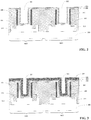
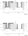
FIG. 2 through FIG. 14 are simplified cross-sectional views of intermediate stages of a semiconductor device manufactured by a method according to some embodiments of the present invention. - In the following description, numerous specific details are provided for a thorough understanding of the present invention. However, it should be appreciated by those of skill in the art that the present invention may be realized without one or more of these details. In other examples, features and techniques known in the art will not be described for purposes of brevity.
- It should be understood that the drawings are not drawn to scale, and similar reference numbers are used for representing similar elements. Embodiments of the invention are described herein with reference to cross-section illustrations that are schematic illustrations of idealized embodiments (and intermediate structures) of the invention. The thickness of layers and regions in the drawings may be exaggerated relative to each other for clarity. Additionally, variations from the shapes of the illustrations as a result, for example, of manufacturing techniques and/or tolerances, are to be expected. Thus, embodiments of the invention should not be construed as limited to the particular shapes of regions illustrated herein, but are to include deviations in shapes that result, for example, from manufacturing.
- It will be understood that, when an element or layer is referred to as "on," "disposed on," "adjacent to," "connected to,"' or "coupled to" another element or layer, it can be disposed directly on the other element or layer, adjacent to, connected or coupled to the other element or layer, or intervening elements or layers may also be present. In contrast, when an element is referred to as being "directly on," directly disposed on," "directly connected to," or "directly coupled to" another element or layer, there are no intervening elements or layers present between them. It will be understood that, although the terms "first," "second," "third," etc. may be used herein to describe various elements, components, regions, layers and/or sections, these elements, components, regions, layers and/or sections should not be limited by these terms. These terms are only used to distinguish one element, component, region, layer or section from another region, layer or section. Thus, a first element, component, region, layer or section discussed below could be termed a second element, component, region, layer or section without departing from the teachings of the present invention.
- Relative terms such as "under," "below," "underneath," "over," "on," "above," "bottom," and "top" are used herein to described a relationship of one element, layer or region to another element, layer or region as illustrated in the figures. It will be understood that these terms are intended to encompass different orientations of the structure in addition to the orientation depicted in the figures. For example, if the device shown in the figures is flipped, the description of an element being "below" or "underneath" another element would then be oriented as "above" the other element. Therefore, the term "below," "under," or "underneath" can encompass both orientations of the device. Because devices or components of embodiments of the present invention can be positioned in a number of different orientations (e.g., rotated 90 degrees or at other orientations), the relative terms should be interpreted accordingly.
- The terms "a", "an" and "the" may include singular and plural references. It will be further understood that the terms "comprising", "including", having" and variants thereof, when used in this specification, specify the presence of stated features, steps, operations, elements, and/or components, but do not preclude the presence or addition of one or more other features, steps, operations, elements, components, and/or groups thereof. Furthermore, as used herein, the words "and/or" may refer to and encompass any possible combinations of one or more of the associated listed items.
- The use of the terms first, second, etc. do not denote any order, but rather the terms first, second, etc. are used to distinguish one element from another. Furthermore, the use of the terms a, an, etc. does not denote a limitation of quantity, but rather denote the presence of at least one of the referenced items.
- Embodiments of the invention are described herein with reference to cross-section illustrations that are schematic illustrations of idealized embodiments (and intermediate structures) of the invention. The thickness of layers and regions in the drawings may be exaggerated for clarity. Additionally, variations from the shapes of the illustrations as a result, for example, of manufacturing techniques and/or tolerances, are to be expected. Thus, embodiments of the invention should not be construed as limited to the particular shapes of regions illustrated herein, but are to include deviations in shapes that result, for example, from manufacturing. For example, an implanted region illustrated as a rectangle will, typically, have rounded or curved features and/or a gradient of implant concentration at its edges rather than a discrete change from implanted to non-implanted region. Likewise, a buried region formed by implantation may result in some implantation in the region between the buried region and the surface through which the implantation takes place. Thus, the regions illustrated in the figures are schematic in nature and their shapes are not intended to illustrate the actual shape of a region of a device and are not intended to limit the invention.
- The present invention will now be described more fully herein after with reference to the accompanying drawings, in which preferred embodiments of the invention are shown. This invention may, however, be embodied in many different forms and should not be construed as limited by the embodiments set forth herein. Rather, these embodiments are provided so that this disclosure will be thorough and complete, and will fully convey the invention to those skilled in the art.
-
FIG. 1 is a simplified flowchart illustrating a method for manufacturing of a semiconductor device according to one embodiment of the present invention.FIG. 2 through FIG. 14 are simplified cross-sectional views of intermediate stages of a semiconductor device manufactured by a method according to some embodiments of the present invention. The manufacturing method of a semiconductor device according to embodiments of the present invention will be described in detail with reference toFIG. 1 andFIG. 2 throughFIG. 14 . - Referring to
FIG. 1 , instep 102, a substrate structure is provided. -
FIG. 2 is a simplified cross-sectional view of an intermediate stage of a substrate structure according to one embodiment of the present invention. As shown inFIG. 2 , the substrate structure includes a PMOS region having afirst trench 201 and an NMOS region having asecond trench 202 on asubstrate 200. The PMOS region and the NMOS region may be isolated from each other by an isolation structure, such as a shallow trench isolation structure. A high-k dielectric layer 203 is formed at the bottom and on sidewalls offirst trench 201 andsecond trench 202. A first P-type work functionlayer adjustment layer 204 is formed on high-k dielectric layer 203. In one embodiment, the substrate structure includes afirst semiconductor fin 211 disposed between the substrate and the first trench, and asecond semiconductor fin 212 disposed between the substrate and the second trench. In one embodiment, second andsecond semiconductor fins substrate 200 and in respective first andsecond trenches second fins - In one embodiment, the method for manufacturing the above-described substrate structure may include the following steps:
- S1: providing an initial substrate structure including a PMOS region having a
first trench 201 and an NMOS region having asecond trench 202. The first and second trenches may be formed, for example, using the following steps: forming a dummy gate oxide layer on a surface of the substrate having the PMOS and NMOS regions, forming a dummy gate on the PMOS region and a dummy gate on the NMOS region, formingspacers 206 on sidewalls of the dummy gates, forming aninterlayer dielectric layer 205 on the dummy gates, after forminginterlayer dielectric layer 205, a planarization process is performed to expose the dummy gate in the PMOS region and the dummy gate in in the NMOS region. Thereafter, the dummy gates and the dummy gate oxide layer underneath the dummy gates are removed to form first andsecond trenches Spacers 206 are retained on the sidewalls of first andsecond trenches Spacers 206 may include, for example, silicon oxide, silicon nitride, silicon oxynitride, or the like. - S2: forming a high-k dielectric layer 203 (e.g., using a deposition process) on the bottom and side surfaces of first and
second trenches k dielectric layer 203, an interface layer (IL), such as a thermal oxide layer by thermal oxidation, may be formed on the bottom surface of first andsecond trenches second trenches k dielectric layer 203. - S3: forming a first P-type work function dielectric layer 204 (e.g., using a deposition process) on high-
k dielectric layer 203 to form the substrate structure. - In another embodiment, the method may further include, between steps S2 and S3, the following steps:
- S4: forming a cap layer on high-
k dielectric layer 203, e.g., using a deposition process. The cap layer may include a TiN layer and an amorphous silicon layer on the TiN layer. Thereafter, a spike annealing process may be performed at a temperature in the range between 800 °C and 1000 °C, e.g., 900 °C, 950 °C. - S5: removing the cap layer.
- In this embodiment, forming the cap layer on the high-k dielectric layer and then removing the cap layer may improve the performance of the high-k dielectric layer, thereby increasing the reliability of the semiconductor device.
- Further, as shown in
FIG. 2 , a raised source/drain region 221 and a raised source/drain region 222 are formed on opposite sides of thefirst semiconductor fin 211 infirst trench 201 and on opposite sides of thesecond semiconductor fin 212 insecond trench 202. In the PMOS region, raised source/drain region 221 may be formed by epitaxially growing SiGe, which may introduce compressive stress into a channel region, thereby increasing the mobility of holes. In the NMOS region, raised source/drain region 222 may be formed by epitaxially growing SiC or Si, which may introduce tensile stress into the channel region, thereby increasing the mobility of electrons. - Referring back to
FIG. 1 , instep 104, a firstprotective layer 301 and a secondprotective layer 302 are sequentially formed on the substrate structure, as shown inFIG. 3 . In one embodiment, firstprotective layer 301 may include a silicon oxide, such as silicon dioxide. Secondprotective layer 302 may include amorphous silicon or polycrystalline silicon. In a preferred embodiment, secondprotective layer 302 includes amorphous silicon. It is to be understood that firstprotective layer 301 and secondprotective layer 302 are not limited to the above-described materials, and those of skill in the art may choose suitable materials as protective materials according to actual requirements. Further, firstprotective layer 301 has a thickness in the range between 5 Angstroms and 15 Angstroms, e.g., 10 Angstroms. Secondprotective layer 302 has a thickness in the range between 15 Angstroms and 25 Angstroms, e.g., 20 Angstroms. - Thereafter, in
step 106, amask layer 401 is formed (e.g., by deposition) on secondprotective layer 302, as shown inFIG. 4 .Mask layer 401 may include, for example, a photoresist. In a preferred embodiment, the bottom of the photoresist may have a bottom anti reflective coating (BARC) and the top of the photoresist may have a top anti reflective coating (TARC). - Next, in
step 108, a portion ofmask layer 401 on the NMOS region is removed using a dry etching process to expose a portion of secondprotective layer 302 on the NMOS region, as shown inFIG. 5 . Because the NMOS region is protected by firstprotective layer 301 and secondprotective layer 302 while a portion ofmask layer 401 on the NMOS region is removed, so that the damage caused by the dry plasma etching to the high-k dielectric layer of the NMOS is reduced. - Next, in
step 110, a portion of secondprotective layer 302 on the NMOS region is removed to expose a portion of firstprotective layer 301 on the NMOS region, as shown inFIG. 6 . In one embodiment, the portion of secondprotective layer 302 on the NMOS region may be removed by a wet etching process, for example, using NH4OH or TMAH as an etching solution. - Next, in
step 112,mask layer 401 on the PMOS region is removed using a dry etching process to expose secondprotective layer 302 on the PMOS region, as shown inFIG. 7 . Because the PMOS region is protected by firstprotective layer 301 and secondprotective layer 302 and the NMOS region is protected by firstprotective layer 301, the damage caused by the dry plasma etching to the high-k dielectric layer of the PMOS and NMOS regions is reduced. - Next, in
step 114, the exposed portion of firstprotective layer 301 on the NMOS region is removed to expose a portion of the first P-type workfunction adjustment layer 204 on the NMOS region, as shown inFIG. 8 . Thereafter, the exposed portion of first P-type workfunction adjustment layer 204 on the NMOS region is removed, as shown inFIG. 9 . In one embodiment, the exposed portion of firstprotective layer 301 on the NMOS region may be removed using a wet etching process, e.g., using dilute hydrofluoric acid (HF). In addition, the portion of first P-type workfunction adjustment layer 204 on the NMOS region may be removed using a SC1 or SC2 cleaning solution. Herein, the SC1 cleaning solution may include, for example, ammonium hydroxide, hydrogen peroxide, deionized water, and the like. The SC2 solution may include, for example, hydrochloric acid, hydrogen peroxide, deionized water, and the like. - Next, in
step 116, the portion of secondprotective layer 302 and the portion of firstprotective layer 301 on the PMOS region are removed, as shown inFIG. 10 . In one embodiment, the portion of secondprotective layer 302 and the portion of firstprotective layer 301 on the PMOS region may be removed using a wet etching process. In an exemplary embodiment, the portion of secondprotective layer 302 on the PMOS region may be removed using NH4OH or TMAH as an etching solution, and , the portion of firstprotective layer 301 on the PMOS region may be removed using a wet etching process, e.g., using dilute hydrofluoric acid (HF). - Thus, a method of manufacturing a semiconductor device according to one embodiment of the present invention has been described above. According to the method, when the mask layer on the NMOS region is removed using a dry etching process, the first protective layer may reduce the damage of the high-k dielectric layer caused by the dry plasma etching is reduced. When removing the mask layer on the PMOS region, the first and second protective layers may reduce the damage caused by the plasma dry etching to the high-k dielectric layer of the PMOS and NMOS regions, thus, improving the device performance.
-
FIGS. 11 through 14 are cross-sectional views of intermediate stages of subsequent processes according to some embodiments of the present invention. - Referring to
FIG. 11 , a second P-type workfunction adjustment layer 1101 is formed on the portion of first P-type workfunction adjustment layer 204 on the PMOS region and on the portion of high-k dielectric layer 203 on the NMOS region. Second P-type workfunction adjustment layer 1101 may include, but is not limited to, TiN, TaN, or TaC and has a thickness in the range between 10 Angstroms and 20 Angstroms, e.g., 15 Angstroms. - Referring to
FIG. 12 , an N-type workfunction adjustment layer 1201 is formed on second P-type workfunction adjustment layer 1101. N-type workfunction adjustment layer 1101 may include, but is not limited to, TiAl, TiCAl, TiNAl, or TiSiAl. - Referring to
FIG. 13 , a metal layer 1301' (e.g., tungsten) is deposited on N-type workfunction adjustment layer 1201 to form a metal electrode. In one embodiment, an adhesive layer, such as TiN, Ti or a stacked structure including TiN and Ti, is formed on N-type workfunction adjustment layer 1201. Thereafter, a metal layer 1301' is deposited on the adhesive layer, so that the bonding between metal layer 1301' and N-type workfunction adjustment layer 1201 is made more compact. - Thereafter, a planarization (e.g., chemical mechanical polishing) process is performed on the metal layer to obtain a
metal electrode 1301. - Referring to
FIG. 14 , according to some embodiments of the present invention, a semiconductor device includes a substrate structure including a PMOS region having a first trench and an NMOS region having a second trench on a substrate, a high-k dielectric layer at a bottom and on sidewalls of the first and second trenches, a first P-type work function adjustment layer on the high-k dielectric layer of the first and second trenches; a second P-type work function adjustment layer on the first P-type work function adjustment layer of the PMOS region; and an N-type work function adjustment layer on the second P-type work function adjustment layer of the PMOS region and on the first P-type work function of the NMOS region. - In one embodiment, the first and second P-type work function adjustment layers each include TiN, TaN, or TaC. The N-type work function adjustment layer includes TiAl, TiCAl, TiNAl, or TiSiAl.
- In one embodiment, the semiconductor device further includes an interface layer formed between the bottom of the first and second trenches and the high-k dielectric layer.
- In one embodiment, the semiconductor device further includes a first semiconductor fin on the substrate; a second semiconductor fin on the substrate; raised source/drain regions on opposites sides of the first and second semiconductor fins.
- In one embodiment, the semiconductor device further includes spacers disposed between the raised source/drain regions and the first and second trenches.
- In one embodiment, the semiconductor device further includes a metal gate on the N-type work function adjustment layer of the first and second trenches.
- In one embodiment, the semiconductor device further includes an adhesive layer disposed between the metal gate and the N-type work function adjustment layer.
- Thus, embodiments of the present invention provide detailed description of a method for manufacturing a semiconductor device. In the description, numerous specific details such as forming a raised source/drain region, forming a protective layer by deposition, and the like have not been described in detail in order not to obscure the embodiments of the invention.
- References in the specification to "one embodiment", "an embodiment", "an example embodiment", "some embodiments", etc., indicate that the embodiment described may include a particular feature, structure, or characteristic, but every embodiment may not necessarily include the particular feature, structure, or characteristic. Moreover, such phrases are not necessarily referring to the same embodiment. Further, when a particular feature, structure, or characteristic is described in connection with an embodiment, it is submitted that it is within the knowledge of one skilled in the art to affect such feature, structure, or characteristic in connection with other embodiments whether or not explicitly described.
- While the present invention is described herein with reference to illustrative embodiments, this description is not intended to be construed in a limiting sense. Rather, the purpose of the illustrative embodiments is to make the present invention be better understood by those skilled in the art. In order not to obscure the invention, many details of well-known processes and manufacturing techniques are omitted. Various modifications of the illustrative embodiments as well as other embodiments will be apparent to those of skill in the art upon reference to the description. It is therefore intended that the appended claims encompass any such modifications.
- Furthermore, some of the features of the preferred embodiments of the present invention could be used to advantage without the corresponding use of other features. As such, the foregoing description should be considered as merely illustrative of the principles of the invention, and not in limitation thereof.
Claims (15)
- A method of manufacturing a semiconductor device, the method comprising:providing a substrate structure including a PMOS region having a first trench and an NMOS region having a second trench, a high-k dielectric layer at a bottom and on sidewalls of the first and second trenches, and a first P-type work function adjustment layer on the high-k dielectric layer;forming a first protective layer on the substrate structure and a second protective layer on the first protective layer;forming a mask layer on the second protective layer;removing a portion of the mask layer on the NMOS region using a first dry etching process to expose a portion of the second protective layer on the NMOS region;removing the exposed portion of the second protective layer on the NMOS region to exposed a portion of the first protective layer on the NMOS region;removing the mask layer on the PMOS region using a second dry etching process to expose the second protective layer on the PMOS region;removing a portion of the first protective layer and a portion of the first P-type work function adjustment layer on the NMOS region; andremoving the second protective layer and the first protective layer on the PMOS region.
- The method of claim 1, wherein at least one of::the first protective layer comprises silicon oxide, and the second protective layer comprises amorphous silicon or polycrystalline silicon; andthe substrate structure further comprises an interface layer formed between the bottom of the first and second trenches and the high-k dielectric layer.
- The method of claim 1 or 2, wherein removing the first protective layer on the NMOS region and on the PMOS region comprises a dilute hydrofluoric acid (HF).
- The method of anyone of the claims 1-3, wherein removing the second protective layer on the NMOS region and on the PMOS region comprises an etching solution of NH4OH or TMAH.
- The method of anyone of the claims 1-4, wherein the first trench comprises a first semiconductor fin, and the second trench comprises a second semiconductor fin, the method further comprising:sequentially forming the high-k dielectric layer and the first P-type work function adjustment layer on an upper surface and on side surfaces of the first and second semiconductor fins.
- The method of anyone of the claims 1-5, wherein providing the substrate structure comprises:providing an initial substrate structure including the PMOS region having the first trench and the NMOS region having the second trench;forming the high-k dielectric layer at the bottom and on the sidewalls of the first and second trenches;forming a cap layer on the high-k dielectric layer, the cap layer comprising a TiN layer and an amorphous layer on the TiN layer; andremoving the cap layer to obtain the substrate structure.
- The method of anyone of the claims 1-6, further comprising:forming a second P-type work function adjustment layer on the portion of the first P-type work function adjustment layer on the PMOS region and on the portion of the high-k dielectric layer on the NMOS region;forming an N-type work function adjustment layer on the second P-type work function adjustment layer; andforming a metal layer on the N-type work function adjustment layer.
- The method of claim 7, wherein forming the metal layer on the N-type work function adjustment layer comprises:forming an adhesive layer on the N-type work function adjustment layer;forming the metal layer on the adhesive layer.
- The method of claim 7 or 8, further comprising:planarizing the metal layer to form a metal gate.
- The method of anyone of the claims 7-9, wherein at least one of:the first P-type work function adjustment layer comprises TiN, TaN, or TaC;the second P-type work function adjustment layer comprises TiN, TaN, or TaC; andthe N-type work function adjustment layer comprises TiAl, TiCAl, TiNAl, or TiSiAl.
- A semiconductor device, comprising:a substrate structure including a PMOS region having a first trench and an NMOS region having a second trench on a substrate;a high-k dielectric layer at a bottom and on sidewalls of the first and second trenches;a first P-type work function adjustment layer on the high-k dielectric layer of the first and second trenches;a second P-type work function adjustment layer on the first P-type work function adjustment layer of the PMOS region;an N-type work function adjustment layer on the second P-type work function adjustment layer of the PMOS region and on the first P-type work function of the NMOS region.
- The semiconductor device of claim 11, wherein- the first P-type work function adjustment layer comprises TiN, TaN, or TaC, and the second P-type work function adjustment layer comprises TiN, TaN, or TaC; and/or- the N-type work function adjustment layer comprises TiAl, TiCAl, TiNAl, or TiSiAl.
- The semiconductor device of claim 12 or 11, further comprising at least one of:- an interface layer formed between the bottom of the first and second trenches and the high-k dielectric layer.
- The semiconductor device of anyone of the claim 12-13, further comprising:a first semiconductor fin on the substrate, a second semiconductor fin on the substrate, and raised source/drain regions on opposites sides of the first and second semiconductor fins, andpreferably: spacers disposed between the raised source/drain regions and the first and second trenches.
- The semiconductor device of anyone of the claims 12-14, further comprising
a metal gate on the N-type work function adjustment layer of the first and second trenches, and
preferably: an adhesive layer disposed between the metal gate and the N-type work function adjustment layer.
Applications Claiming Priority (1)
| Application Number | Priority Date | Filing Date | Title |
|---|---|---|---|
| CN201610927451.9A CN108022874B (en) | 2016-10-31 | 2016-10-31 | Method for manufacturing semiconductor device |
Publications (3)
| Publication Number | Publication Date |
|---|---|
| EP3316289A2 true EP3316289A2 (en) | 2018-05-02 |
| EP3316289A3 EP3316289A3 (en) | 2018-07-18 |
| EP3316289B1 EP3316289B1 (en) | 2021-09-08 |
Family
ID=60201384
Family Applications (1)
| Application Number | Title | Priority Date | Filing Date |
|---|---|---|---|
| EP17199137.5A Not-in-force EP3316289B1 (en) | 2016-10-31 | 2017-10-30 | Method to improve the quality of a high-k dielectric layer |
Country Status (3)
| Country | Link |
|---|---|
| US (1) | US20180122806A1 (en) |
| EP (1) | EP3316289B1 (en) |
| CN (1) | CN108022874B (en) |
Families Citing this family (9)
| Publication number | Priority date | Publication date | Assignee | Title |
|---|---|---|---|---|
| US10930778B2 (en) | 2018-10-11 | 2021-02-23 | International Business Machines Corporation | Vertical transistor devices with composite high-K and low-K spacers with a controlled top junction |
| CN112151451B (en) * | 2019-06-28 | 2025-03-21 | 中芯国际集成电路制造(上海)有限公司 | Semiconductor structure and method of forming the same |
| CN112951766B (en) * | 2019-12-11 | 2025-03-21 | 中芯国际集成电路制造(上海)有限公司 | Semiconductor structure and method of forming the same |
| US11489056B2 (en) * | 2020-02-10 | 2022-11-01 | Taiwan Semiconductor Manufacturing Co., Ltd. | Semiconductor device with multi-threshold gate structure |
| US11848239B2 (en) * | 2020-07-10 | 2023-12-19 | Taiwan Semiconductor Manufacturing Co., Ltd. | Patterning method and structures resulting therefrom |
| US20220093596A1 (en) * | 2020-09-23 | 2022-03-24 | Intel Corporation | Fabrication of gate-all-around integrated circuit structures having common metal gates and having gate dielectrics with a dipole layer |
| US11610818B2 (en) * | 2021-01-28 | 2023-03-21 | Taiwan Semiconductor Manufacturing Company Ltd. | Semiconductor structure and method for forming the same |
| CN115132660B (en) * | 2021-03-25 | 2025-11-28 | 中芯国际集成电路制造(上海)有限公司 | Methods for forming semiconductor structures |
| US12324139B2 (en) * | 2022-01-12 | 2025-06-03 | Changxin Memory Technologies, Inc. | Method for manufacturing semiconductor device and semiconductor device |
Family Cites Families (13)
| Publication number | Priority date | Publication date | Assignee | Title |
|---|---|---|---|---|
| KR100620651B1 (en) * | 2000-06-22 | 2006-09-13 | 주식회사 하이닉스반도체 | Manufacturing method of fine pattern of semiconductor device |
| US20110175168A1 (en) * | 2008-08-08 | 2011-07-21 | Texas Instruments Incorporated | Nmos transistor with enhanced stress gate |
| US7732344B1 (en) * | 2009-06-05 | 2010-06-08 | Taiwan Semiconductor Manufacturing Company, Ltd. | High selectivity etching process for metal gate N/P patterning |
| KR101909091B1 (en) * | 2012-05-11 | 2018-10-17 | 삼성전자 주식회사 | Semiconductor device and fabricating method thereof |
| KR20140006204A (en) * | 2012-06-27 | 2014-01-16 | 삼성전자주식회사 | Semiconductor device and fabricating method thereof |
| KR101923946B1 (en) * | 2012-08-31 | 2018-11-30 | 삼성전자 주식회사 | Semiconductor device and method for fabricating the same |
| CN104217954A (en) * | 2013-06-05 | 2014-12-17 | 中芯国际集成电路制造(上海)有限公司 | Formation method of transistors |
| CN105244318B (en) * | 2014-07-09 | 2018-07-20 | 中芯国际集成电路制造(上海)有限公司 | A kind of semiconductor devices and its manufacturing method and electronic device |
| US9330938B2 (en) * | 2014-07-24 | 2016-05-03 | International Business Machines Corporation | Method of patterning dopant films in high-k dielectrics in a soft mask integration scheme |
| US20160086805A1 (en) * | 2014-09-24 | 2016-03-24 | Qualcomm Incorporated | Metal-gate with an amorphous metal layer |
| KR102235612B1 (en) * | 2015-01-29 | 2021-04-02 | 삼성전자주식회사 | Semiconductor device having work-function metal and method of forming the same |
| US9337104B1 (en) * | 2015-05-11 | 2016-05-10 | Semiconductor Manufacturing International (Shanghai) Corporation | Method for chemical mechanical polishing of high-K metal gate structures |
| CN107492498B (en) * | 2016-06-13 | 2020-03-10 | 中芯国际集成电路制造(上海)有限公司 | How to form a fin field effect transistor |
-
2016
- 2016-10-31 CN CN201610927451.9A patent/CN108022874B/en active Active
-
2017
- 2017-04-18 US US15/489,772 patent/US20180122806A1/en not_active Abandoned
- 2017-10-30 EP EP17199137.5A patent/EP3316289B1/en not_active Not-in-force
Non-Patent Citations (1)
| Title |
|---|
| None |
Also Published As
| Publication number | Publication date |
|---|---|
| CN108022874B (en) | 2021-02-09 |
| EP3316289A3 (en) | 2018-07-18 |
| CN108022874A (en) | 2018-05-11 |
| US20180122806A1 (en) | 2018-05-03 |
| EP3316289B1 (en) | 2021-09-08 |
Similar Documents
| Publication | Publication Date | Title |
|---|---|---|
| EP3316289B1 (en) | Method to improve the quality of a high-k dielectric layer | |
| US10181427B2 (en) | Semiconductor devices and methods for fabricating the same | |
| US10211309B2 (en) | Method and device for metal gate stacks | |
| CN105321883B (en) | Method for manufacturing semiconductor device | |
| US10680079B2 (en) | Semiconductor structure and fabrication method thereof | |
| US10204985B2 (en) | Structure and formation method of semiconductor device structure | |
| US20140248761A1 (en) | Semiconductor device having dual metal silicide layers and method of manufacturing the same | |
| US8802523B2 (en) | CMOS device and fabrication method | |
| US10867799B2 (en) | FinFET device and methods of forming same | |
| CN106409679A (en) | Finfet with doped isolation insulating layer | |
| US8921171B2 (en) | Method for forming gate structure, method for forming semiconductor device, and semiconductor device | |
| TWI804880B (en) | Semiconductor device and method | |
| EP3316286A1 (en) | Dummy gate structures and manufacturing method thereof | |
| CN104752447A (en) | Semiconductor device and manufacturing method thereof | |
| CN119153411A (en) | Method for preparing semiconductor structure and semiconductor structure | |
| KR20170128170A (en) | Semiconductor structure with insertion layer and method for manufacturing the same | |
| US20060157750A1 (en) | Semiconductor device having etch-resistant L-shaped spacer and fabrication method thereof | |
| US20250359163A1 (en) | Device having hybrid nanosheet structure and method | |
| US20200098884A1 (en) | Method to improve hkmg contact resistance | |
| US7323419B2 (en) | Method of fabricating semiconductor device | |
| US20090309161A1 (en) | Semiconductor integrated circuit device | |
| CN107424926B (en) | Semiconductor device and manufacturing method thereof | |
| CN104752316B (en) | A kind of method for making semiconductor devices | |
| US10147649B2 (en) | Semiconductor device structure with gate stack and method for forming the same | |
| CN104835737B (en) | Semiconductor devices and preparation method thereof |
Legal Events
| Date | Code | Title | Description |
|---|---|---|---|
| PUAI | Public reference made under article 153(3) epc to a published international application that has entered the european phase |
Free format text: ORIGINAL CODE: 0009012 |
|
| STAA | Information on the status of an ep patent application or granted ep patent |
Free format text: STATUS: THE APPLICATION HAS BEEN PUBLISHED |
|
| AK | Designated contracting states |
Kind code of ref document: A2 Designated state(s): AL AT BE BG CH CY CZ DE DK EE ES FI FR GB GR HR HU IE IS IT LI LT LU LV MC MK MT NL NO PL PT RO RS SE SI SK SM TR |
|
| AX | Request for extension of the european patent |
Extension state: BA ME |
|
| PUAL | Search report despatched |
Free format text: ORIGINAL CODE: 0009013 |
|
| AK | Designated contracting states |
Kind code of ref document: A3 Designated state(s): AL AT BE BG CH CY CZ DE DK EE ES FI FR GB GR HR HU IE IS IT LI LT LU LV MC MK MT NL NO PL PT RO RS SE SI SK SM TR |
|
| AX | Request for extension of the european patent |
Extension state: BA ME |
|
| RIC1 | Information provided on ipc code assigned before grant |
Ipc: H01L 27/092 20060101ALI20180608BHEP Ipc: H01L 21/28 20060101ALN20180608BHEP Ipc: H01L 21/8238 20060101AFI20180608BHEP |
|
| RAP1 | Party data changed (applicant data changed or rights of an application transferred) |
Owner name: SEMICONDUCTOR MANUFACTURING INTERNATIONAL (SHANGHA Owner name: SEMICONDUCTOR MANUFACTURING INTERNATIONAL (BEIJING |
|
| STAA | Information on the status of an ep patent application or granted ep patent |
Free format text: STATUS: REQUEST FOR EXAMINATION WAS MADE |
|
| 17P | Request for examination filed |
Effective date: 20181220 |
|
| RBV | Designated contracting states (corrected) |
Designated state(s): AL AT BE BG CH CY CZ DE DK EE ES FI FR GB GR HR HU IE IS IT LI LT LU LV MC MK MT NL NO PL PT RO RS SE SI SK SM TR |
|
| STAA | Information on the status of an ep patent application or granted ep patent |
Free format text: STATUS: EXAMINATION IS IN PROGRESS |
|
| 17Q | First examination report despatched |
Effective date: 20201203 |
|
| GRAP | Despatch of communication of intention to grant a patent |
Free format text: ORIGINAL CODE: EPIDOSNIGR1 |
|
| STAA | Information on the status of an ep patent application or granted ep patent |
Free format text: STATUS: GRANT OF PATENT IS INTENDED |
|
| RIC1 | Information provided on ipc code assigned before grant |
Ipc: H01L 21/28 20060101ALN20210310BHEP Ipc: H01L 29/49 20060101ALI20210310BHEP Ipc: H01L 27/092 20060101ALI20210310BHEP Ipc: H01L 21/8238 20060101AFI20210310BHEP |
|
| RIC1 | Information provided on ipc code assigned before grant |
Ipc: H01L 21/28 20060101ALN20210312BHEP Ipc: H01L 29/49 20060101ALI20210312BHEP Ipc: H01L 27/092 20060101ALI20210312BHEP Ipc: H01L 21/8238 20060101AFI20210312BHEP |
|
| RIC1 | Information provided on ipc code assigned before grant |
Ipc: H01L 21/28 20060101ALN20210324BHEP Ipc: H01L 29/49 20060101ALI20210324BHEP Ipc: H01L 27/092 20060101ALI20210324BHEP Ipc: H01L 21/8238 20060101AFI20210324BHEP |
|
| INTG | Intention to grant announced |
Effective date: 20210407 |
|
| RIN1 | Information on inventor provided before grant (corrected) |
Inventor name: LI, YONG |
|
| GRAS | Grant fee paid |
Free format text: ORIGINAL CODE: EPIDOSNIGR3 |
|
| GRAA | (expected) grant |
Free format text: ORIGINAL CODE: 0009210 |
|
| STAA | Information on the status of an ep patent application or granted ep patent |
Free format text: STATUS: THE PATENT HAS BEEN GRANTED |
|
| AK | Designated contracting states |
Kind code of ref document: B1 Designated state(s): AL AT BE BG CH CY CZ DE DK EE ES FI FR GB GR HR HU IE IS IT LI LT LU LV MC MK MT NL NO PL PT RO RS SE SI SK SM TR |
|
| REG | Reference to a national code |
Ref country code: GB Ref legal event code: FG4D |
|
| REG | Reference to a national code |
Ref country code: AT Ref legal event code: REF Ref document number: 1429341 Country of ref document: AT Kind code of ref document: T Effective date: 20210915 Ref country code: CH Ref legal event code: EP |
|
| REG | Reference to a national code |
Ref country code: IE Ref legal event code: FG4D |
|
| REG | Reference to a national code |
Ref country code: DE Ref legal event code: R096 Ref document number: 602017045596 Country of ref document: DE |
|
| REG | Reference to a national code |
Ref country code: LT Ref legal event code: MG9D |
|
| REG | Reference to a national code |
Ref country code: NL Ref legal event code: MP Effective date: 20210908 |
|
| PG25 | Lapsed in a contracting state [announced via postgrant information from national office to epo] |
Ref country code: HR Free format text: LAPSE BECAUSE OF FAILURE TO SUBMIT A TRANSLATION OF THE DESCRIPTION OR TO PAY THE FEE WITHIN THE PRESCRIBED TIME-LIMIT Effective date: 20210908 Ref country code: SE Free format text: LAPSE BECAUSE OF FAILURE TO SUBMIT A TRANSLATION OF THE DESCRIPTION OR TO PAY THE FEE WITHIN THE PRESCRIBED TIME-LIMIT Effective date: 20210908 Ref country code: RS Free format text: LAPSE BECAUSE OF FAILURE TO SUBMIT A TRANSLATION OF THE DESCRIPTION OR TO PAY THE FEE WITHIN THE PRESCRIBED TIME-LIMIT Effective date: 20210908 Ref country code: LT Free format text: LAPSE BECAUSE OF FAILURE TO SUBMIT A TRANSLATION OF THE DESCRIPTION OR TO PAY THE FEE WITHIN THE PRESCRIBED TIME-LIMIT Effective date: 20210908 Ref country code: BG Free format text: LAPSE BECAUSE OF FAILURE TO SUBMIT A TRANSLATION OF THE DESCRIPTION OR TO PAY THE FEE WITHIN THE PRESCRIBED TIME-LIMIT Effective date: 20211208 Ref country code: NO Free format text: LAPSE BECAUSE OF FAILURE TO SUBMIT A TRANSLATION OF THE DESCRIPTION OR TO PAY THE FEE WITHIN THE PRESCRIBED TIME-LIMIT Effective date: 20211208 Ref country code: FI Free format text: LAPSE BECAUSE OF FAILURE TO SUBMIT A TRANSLATION OF THE DESCRIPTION OR TO PAY THE FEE WITHIN THE PRESCRIBED TIME-LIMIT Effective date: 20210908 Ref country code: ES Free format text: LAPSE BECAUSE OF FAILURE TO SUBMIT A TRANSLATION OF THE DESCRIPTION OR TO PAY THE FEE WITHIN THE PRESCRIBED TIME-LIMIT Effective date: 20210908 |
|
| REG | Reference to a national code |
Ref country code: AT Ref legal event code: MK05 Ref document number: 1429341 Country of ref document: AT Kind code of ref document: T Effective date: 20210908 |
|
| PG25 | Lapsed in a contracting state [announced via postgrant information from national office to epo] |
Ref country code: LV Free format text: LAPSE BECAUSE OF FAILURE TO SUBMIT A TRANSLATION OF THE DESCRIPTION OR TO PAY THE FEE WITHIN THE PRESCRIBED TIME-LIMIT Effective date: 20210908 Ref country code: GR Free format text: LAPSE BECAUSE OF FAILURE TO SUBMIT A TRANSLATION OF THE DESCRIPTION OR TO PAY THE FEE WITHIN THE PRESCRIBED TIME-LIMIT Effective date: 20211209 |
|
| PG25 | Lapsed in a contracting state [announced via postgrant information from national office to epo] |
Ref country code: AT Free format text: LAPSE BECAUSE OF FAILURE TO SUBMIT A TRANSLATION OF THE DESCRIPTION OR TO PAY THE FEE WITHIN THE PRESCRIBED TIME-LIMIT Effective date: 20210908 |
|
| REG | Reference to a national code |
Ref country code: DE Ref legal event code: R119 Ref document number: 602017045596 Country of ref document: DE |
|
| REG | Reference to a national code |
Ref country code: CH Ref legal event code: PL |
|
| PG25 | Lapsed in a contracting state [announced via postgrant information from national office to epo] |
Ref country code: IS Free format text: LAPSE BECAUSE OF FAILURE TO SUBMIT A TRANSLATION OF THE DESCRIPTION OR TO PAY THE FEE WITHIN THE PRESCRIBED TIME-LIMIT Effective date: 20220108 Ref country code: SM Free format text: LAPSE BECAUSE OF FAILURE TO SUBMIT A TRANSLATION OF THE DESCRIPTION OR TO PAY THE FEE WITHIN THE PRESCRIBED TIME-LIMIT Effective date: 20210908 Ref country code: SK Free format text: LAPSE BECAUSE OF FAILURE TO SUBMIT A TRANSLATION OF THE DESCRIPTION OR TO PAY THE FEE WITHIN THE PRESCRIBED TIME-LIMIT Effective date: 20210908 Ref country code: RO Free format text: LAPSE BECAUSE OF FAILURE TO SUBMIT A TRANSLATION OF THE DESCRIPTION OR TO PAY THE FEE WITHIN THE PRESCRIBED TIME-LIMIT Effective date: 20210908 Ref country code: PT Free format text: LAPSE BECAUSE OF FAILURE TO SUBMIT A TRANSLATION OF THE DESCRIPTION OR TO PAY THE FEE WITHIN THE PRESCRIBED TIME-LIMIT Effective date: 20220110 Ref country code: PL Free format text: LAPSE BECAUSE OF FAILURE TO SUBMIT A TRANSLATION OF THE DESCRIPTION OR TO PAY THE FEE WITHIN THE PRESCRIBED TIME-LIMIT Effective date: 20210908 Ref country code: NL Free format text: LAPSE BECAUSE OF FAILURE TO SUBMIT A TRANSLATION OF THE DESCRIPTION OR TO PAY THE FEE WITHIN THE PRESCRIBED TIME-LIMIT Effective date: 20210908 Ref country code: EE Free format text: LAPSE BECAUSE OF FAILURE TO SUBMIT A TRANSLATION OF THE DESCRIPTION OR TO PAY THE FEE WITHIN THE PRESCRIBED TIME-LIMIT Effective date: 20210908 Ref country code: CZ Free format text: LAPSE BECAUSE OF FAILURE TO SUBMIT A TRANSLATION OF THE DESCRIPTION OR TO PAY THE FEE WITHIN THE PRESCRIBED TIME-LIMIT Effective date: 20210908 Ref country code: AL Free format text: LAPSE BECAUSE OF FAILURE TO SUBMIT A TRANSLATION OF THE DESCRIPTION OR TO PAY THE FEE WITHIN THE PRESCRIBED TIME-LIMIT Effective date: 20210908 |
|
| REG | Reference to a national code |
Ref country code: BE Ref legal event code: MM Effective date: 20211031 |
|
| PG25 | Lapsed in a contracting state [announced via postgrant information from national office to epo] |
Ref country code: MC Free format text: LAPSE BECAUSE OF FAILURE TO SUBMIT A TRANSLATION OF THE DESCRIPTION OR TO PAY THE FEE WITHIN THE PRESCRIBED TIME-LIMIT Effective date: 20210908 |
|
| PLBE | No opposition filed within time limit |
Free format text: ORIGINAL CODE: 0009261 |
|
| STAA | Information on the status of an ep patent application or granted ep patent |
Free format text: STATUS: NO OPPOSITION FILED WITHIN TIME LIMIT |
|
| PG25 | Lapsed in a contracting state [announced via postgrant information from national office to epo] |
Ref country code: LU Free format text: LAPSE BECAUSE OF NON-PAYMENT OF DUE FEES Effective date: 20211030 Ref country code: DK Free format text: LAPSE BECAUSE OF FAILURE TO SUBMIT A TRANSLATION OF THE DESCRIPTION OR TO PAY THE FEE WITHIN THE PRESCRIBED TIME-LIMIT Effective date: 20210908 Ref country code: DE Free format text: LAPSE BECAUSE OF NON-PAYMENT OF DUE FEES Effective date: 20220503 Ref country code: BE Free format text: LAPSE BECAUSE OF NON-PAYMENT OF DUE FEES Effective date: 20211031 |
|
| 26N | No opposition filed |
Effective date: 20220609 |
|
| GBPC | Gb: european patent ceased through non-payment of renewal fee |
Effective date: 20211208 |
|
| PG25 | Lapsed in a contracting state [announced via postgrant information from national office to epo] |
Ref country code: SI Free format text: LAPSE BECAUSE OF FAILURE TO SUBMIT A TRANSLATION OF THE DESCRIPTION OR TO PAY THE FEE WITHIN THE PRESCRIBED TIME-LIMIT Effective date: 20210908 Ref country code: LI Free format text: LAPSE BECAUSE OF NON-PAYMENT OF DUE FEES Effective date: 20211031 Ref country code: CH Free format text: LAPSE BECAUSE OF NON-PAYMENT OF DUE FEES Effective date: 20211031 |
|
| PG25 | Lapsed in a contracting state [announced via postgrant information from national office to epo] |
Ref country code: IE Free format text: LAPSE BECAUSE OF NON-PAYMENT OF DUE FEES Effective date: 20211030 Ref country code: GB Free format text: LAPSE BECAUSE OF NON-PAYMENT OF DUE FEES Effective date: 20211208 |
|
| PG25 | Lapsed in a contracting state [announced via postgrant information from national office to epo] |
Ref country code: FR Free format text: LAPSE BECAUSE OF NON-PAYMENT OF DUE FEES Effective date: 20211108 |
|
| PG25 | Lapsed in a contracting state [announced via postgrant information from national office to epo] |
Ref country code: IT Free format text: LAPSE BECAUSE OF FAILURE TO SUBMIT A TRANSLATION OF THE DESCRIPTION OR TO PAY THE FEE WITHIN THE PRESCRIBED TIME-LIMIT Effective date: 20210908 |
|
| PG25 | Lapsed in a contracting state [announced via postgrant information from national office to epo] |
Ref country code: HU Free format text: LAPSE BECAUSE OF FAILURE TO SUBMIT A TRANSLATION OF THE DESCRIPTION OR TO PAY THE FEE WITHIN THE PRESCRIBED TIME-LIMIT; INVALID AB INITIO Effective date: 20171030 |
|
| PG25 | Lapsed in a contracting state [announced via postgrant information from national office to epo] |
Ref country code: CY Free format text: LAPSE BECAUSE OF FAILURE TO SUBMIT A TRANSLATION OF THE DESCRIPTION OR TO PAY THE FEE WITHIN THE PRESCRIBED TIME-LIMIT Effective date: 20210908 |
|
| PG25 | Lapsed in a contracting state [announced via postgrant information from national office to epo] |
Ref country code: MK Free format text: LAPSE BECAUSE OF FAILURE TO SUBMIT A TRANSLATION OF THE DESCRIPTION OR TO PAY THE FEE WITHIN THE PRESCRIBED TIME-LIMIT Effective date: 20210908 |
|
| PG25 | Lapsed in a contracting state [announced via postgrant information from national office to epo] |
Ref country code: MT Free format text: LAPSE BECAUSE OF FAILURE TO SUBMIT A TRANSLATION OF THE DESCRIPTION OR TO PAY THE FEE WITHIN THE PRESCRIBED TIME-LIMIT Effective date: 20210908 |
|
| PG25 | Lapsed in a contracting state [announced via postgrant information from national office to epo] |
Ref country code: TR Free format text: LAPSE BECAUSE OF FAILURE TO SUBMIT A TRANSLATION OF THE DESCRIPTION OR TO PAY THE FEE WITHIN THE PRESCRIBED TIME-LIMIT Effective date: 20210908 |