EP3316284A1 - Matrix panel and manufacturing method thereof, and display panel and display device - Google Patents
Matrix panel and manufacturing method thereof, and display panel and display device Download PDFInfo
- Publication number
- EP3316284A1 EP3316284A1 EP15892061.1A EP15892061A EP3316284A1 EP 3316284 A1 EP3316284 A1 EP 3316284A1 EP 15892061 A EP15892061 A EP 15892061A EP 3316284 A1 EP3316284 A1 EP 3316284A1
- Authority
- EP
- European Patent Office
- Prior art keywords
- connection line
- conductive pattern
- pattern
- electrode metal
- metal
- Prior art date
- Legal status (The legal status is an assumption and is not a legal conclusion. Google has not performed a legal analysis and makes no representation as to the accuracy of the status listed.)
- Granted
Links
Images






Classifications
-
- H—ELECTRICITY
- H10—SEMICONDUCTOR DEVICES; ELECTRIC SOLID-STATE DEVICES NOT OTHERWISE PROVIDED FOR
- H10D—INORGANIC ELECTRIC SEMICONDUCTOR DEVICES
- H10D86/00—Integrated devices formed in or on insulating or conducting substrates, e.g. formed in silicon-on-insulator [SOI] substrates or on stainless steel or glass substrates
- H10D86/01—Manufacture or treatment
- H10D86/021—Manufacture or treatment of multiple TFTs
-
- H—ELECTRICITY
- H10—SEMICONDUCTOR DEVICES; ELECTRIC SOLID-STATE DEVICES NOT OTHERWISE PROVIDED FOR
- H10D—INORGANIC ELECTRIC SEMICONDUCTOR DEVICES
- H10D30/00—Field-effect transistors [FET]
- H10D30/60—Insulated-gate field-effect transistors [IGFET]
- H10D30/67—Thin-film transistors [TFT]
- H10D30/6729—Thin-film transistors [TFT] characterised by the electrodes
-
- G—PHYSICS
- G02—OPTICS
- G02F—OPTICAL DEVICES OR ARRANGEMENTS FOR THE CONTROL OF LIGHT BY MODIFICATION OF THE OPTICAL PROPERTIES OF THE MEDIA OF THE ELEMENTS INVOLVED THEREIN; NON-LINEAR OPTICS; FREQUENCY-CHANGING OF LIGHT; OPTICAL LOGIC ELEMENTS; OPTICAL ANALOGUE/DIGITAL CONVERTERS
- G02F1/00—Devices or arrangements for the control of the intensity, colour, phase, polarisation or direction of light arriving from an independent light source, e.g. switching, gating or modulating; Non-linear optics
- G02F1/01—Devices or arrangements for the control of the intensity, colour, phase, polarisation or direction of light arriving from an independent light source, e.g. switching, gating or modulating; Non-linear optics for the control of the intensity, phase, polarisation or colour
- G02F1/13—Devices or arrangements for the control of the intensity, colour, phase, polarisation or direction of light arriving from an independent light source, e.g. switching, gating or modulating; Non-linear optics for the control of the intensity, phase, polarisation or colour based on liquid crystals, e.g. single liquid crystal display cells
- G02F1/133—Constructional arrangements; Operation of liquid crystal cells; Circuit arrangements
- G02F1/136—Liquid crystal cells structurally associated with a semi-conducting layer or substrate, e.g. cells forming part of an integrated circuit
- G02F1/1362—Active matrix addressed cells
- G02F1/136204—Arrangements to prevent high voltage or static electricity failures
-
- H—ELECTRICITY
- H10—SEMICONDUCTOR DEVICES; ELECTRIC SOLID-STATE DEVICES NOT OTHERWISE PROVIDED FOR
- H10D—INORGANIC ELECTRIC SEMICONDUCTOR DEVICES
- H10D30/00—Field-effect transistors [FET]
- H10D30/60—Insulated-gate field-effect transistors [IGFET]
- H10D30/67—Thin-film transistors [TFT]
- H10D30/6704—Thin-film transistors [TFT] having supplementary regions or layers in the thin films or in the insulated bulk substrates for controlling properties of the device
-
- H—ELECTRICITY
- H10—SEMICONDUCTOR DEVICES; ELECTRIC SOLID-STATE DEVICES NOT OTHERWISE PROVIDED FOR
- H10D—INORGANIC ELECTRIC SEMICONDUCTOR DEVICES
- H10D30/00—Field-effect transistors [FET]
- H10D30/60—Insulated-gate field-effect transistors [IGFET]
- H10D30/67—Thin-film transistors [TFT]
- H10D30/6757—Thin-film transistors [TFT] characterised by the structure of the channel, e.g. transverse or longitudinal shape or doping profile
-
- H—ELECTRICITY
- H10—SEMICONDUCTOR DEVICES; ELECTRIC SOLID-STATE DEVICES NOT OTHERWISE PROVIDED FOR
- H10D—INORGANIC ELECTRIC SEMICONDUCTOR DEVICES
- H10D86/00—Integrated devices formed in or on insulating or conducting substrates, e.g. formed in silicon-on-insulator [SOI] substrates or on stainless steel or glass substrates
- H10D86/201—Integrated devices formed in or on insulating or conducting substrates, e.g. formed in silicon-on-insulator [SOI] substrates or on stainless steel or glass substrates the substrates comprising an insulating layer on a semiconductor body, e.g. SOI
-
- H—ELECTRICITY
- H10—SEMICONDUCTOR DEVICES; ELECTRIC SOLID-STATE DEVICES NOT OTHERWISE PROVIDED FOR
- H10D—INORGANIC ELECTRIC SEMICONDUCTOR DEVICES
- H10D86/00—Integrated devices formed in or on insulating or conducting substrates, e.g. formed in silicon-on-insulator [SOI] substrates or on stainless steel or glass substrates
- H10D86/40—Integrated devices formed in or on insulating or conducting substrates, e.g. formed in silicon-on-insulator [SOI] substrates or on stainless steel or glass substrates characterised by multiple TFTs
-
- H—ELECTRICITY
- H10—SEMICONDUCTOR DEVICES; ELECTRIC SOLID-STATE DEVICES NOT OTHERWISE PROVIDED FOR
- H10D—INORGANIC ELECTRIC SEMICONDUCTOR DEVICES
- H10D86/00—Integrated devices formed in or on insulating or conducting substrates, e.g. formed in silicon-on-insulator [SOI] substrates or on stainless steel or glass substrates
- H10D86/40—Integrated devices formed in or on insulating or conducting substrates, e.g. formed in silicon-on-insulator [SOI] substrates or on stainless steel or glass substrates characterised by multiple TFTs
- H10D86/441—Interconnections, e.g. scanning lines
-
- H—ELECTRICITY
- H10—SEMICONDUCTOR DEVICES; ELECTRIC SOLID-STATE DEVICES NOT OTHERWISE PROVIDED FOR
- H10D—INORGANIC ELECTRIC SEMICONDUCTOR DEVICES
- H10D86/00—Integrated devices formed in or on insulating or conducting substrates, e.g. formed in silicon-on-insulator [SOI] substrates or on stainless steel or glass substrates
- H10D86/40—Integrated devices formed in or on insulating or conducting substrates, e.g. formed in silicon-on-insulator [SOI] substrates or on stainless steel or glass substrates characterised by multiple TFTs
- H10D86/60—Integrated devices formed in or on insulating or conducting substrates, e.g. formed in silicon-on-insulator [SOI] substrates or on stainless steel or glass substrates characterised by multiple TFTs wherein the TFTs are in active matrices
-
- H—ELECTRICITY
- H10—SEMICONDUCTOR DEVICES; ELECTRIC SOLID-STATE DEVICES NOT OTHERWISE PROVIDED FOR
- H10D—INORGANIC ELECTRIC SEMICONDUCTOR DEVICES
- H10D89/00—Aspects of integrated devices not covered by groups H10D84/00 - H10D88/00
- H10D89/60—Integrated devices comprising arrangements for electrical or thermal protection, e.g. protection circuits against electrostatic discharge [ESD]
- H10D89/601—Integrated devices comprising arrangements for electrical or thermal protection, e.g. protection circuits against electrostatic discharge [ESD] for devices having insulated gate electrodes, e.g. for IGFETs or IGBTs
- H10D89/911—Integrated devices comprising arrangements for electrical or thermal protection, e.g. protection circuits against electrostatic discharge [ESD] for devices having insulated gate electrodes, e.g. for IGFETs or IGBTs using passive elements as protective elements
-
- G—PHYSICS
- G02—OPTICS
- G02F—OPTICAL DEVICES OR ARRANGEMENTS FOR THE CONTROL OF LIGHT BY MODIFICATION OF THE OPTICAL PROPERTIES OF THE MEDIA OF THE ELEMENTS INVOLVED THEREIN; NON-LINEAR OPTICS; FREQUENCY-CHANGING OF LIGHT; OPTICAL LOGIC ELEMENTS; OPTICAL ANALOGUE/DIGITAL CONVERTERS
- G02F1/00—Devices or arrangements for the control of the intensity, colour, phase, polarisation or direction of light arriving from an independent light source, e.g. switching, gating or modulating; Non-linear optics
- G02F1/01—Devices or arrangements for the control of the intensity, colour, phase, polarisation or direction of light arriving from an independent light source, e.g. switching, gating or modulating; Non-linear optics for the control of the intensity, phase, polarisation or colour
- G02F1/13—Devices or arrangements for the control of the intensity, colour, phase, polarisation or direction of light arriving from an independent light source, e.g. switching, gating or modulating; Non-linear optics for the control of the intensity, phase, polarisation or colour based on liquid crystals, e.g. single liquid crystal display cells
- G02F1/133—Constructional arrangements; Operation of liquid crystal cells; Circuit arrangements
- G02F1/1333—Constructional arrangements; Manufacturing methods
- G02F1/1343—Electrodes
- G02F1/134309—Electrodes characterised by their geometrical arrangement
- G02F1/134372—Electrodes characterised by their geometrical arrangement for fringe field switching [FFS] where the common electrode is not patterned
Definitions
- the first conductive pattern includes a first gate electrode metal pattern
- the second conductive pattern includes a second gate electrode metal pattern
- the gate electrode metal pattern includes a gate electrode and a gate line
- the metal connection line 103 provided by the embodiment is connected with the first gate electrode metal pattern 101 and the second gate electrode metal pattern 102 to make a voltage of the first gate electrode metal pattern 101 and a voltage of the second gate electrode metal pattern 102 in a technological process kept to be the same, and therefore an electric potential difference between the first gate electrode metal pattern 101 and the second gate electrode metal pattern 102 can be balanced, an electrostatic discharge phenomenon is avoided, finally, endurance capacity of a product on the electrostatic discharge phenomenon is improved, and a product yield is increased.
- Step 1001 forming a first conductive pattern, a second conductive pattern and a metal connection line on a base substrate, the metal connection line being connected with the first conductive pattern and the second conductive pattern.
- a transparent electrode 106 is formed above the active layer 104.
- a source electrode metal pattern and a drain electrode metal pattern are formed above the active layer 104, the source electrode metal pattern includes a source electrode and a data line, and the drain electrode metal pattern includes a drain electrode.
- the source electrode metal pattern and the drain electrode metal pattern are jointly called a source and drain electrode metal pattern.
- a passivation layer 108 is formed above the source and drain electrode metal pattern 107 and the first transparent electrode 106, a first via hole 105 corresponding to the meal connection line 103 is opened in the passivation layer 108, and the metal connection line 103 is exposed through the first via hole 105.
- a transparent electrode thin film is formed above the passivation layer 108, the transparent electrode thin film and the metal connection line 103 are etched to form a second transparent electrode 109.
- an etching process comprises wet etching.
- the metal connection line 103 is removed through the etching process to make the first gate electrode metal pattern 101 and the second gate electrode metal pattern 102 disconnected, therefore avoiding influence on work performance of the first gate electrode metal pattern 101 and work performance of the second gate electrode metal pattern 102.
- what is connected with the drain electrode is a pixel electrode, and the other is a common electrode.
- the manufacturing method of the array substrate provided by the embodiment comprises: forming the first conductive pattern, the second conductive pattern and the metal connection line on the base substrate, the metal connection line being connected with the first conductive pattern and the second conductive pattern; and etching the metal connection line to make the first conductive pattern and the second conductive pattern insulated from each other.
- the metal connection line provided by the embodiment is connected with the first conductive pattern and the second conductive pattern to make a voltage of the first conductive pattern and a voltage of the second conductive pattern in the technological process kept to be the same, and therefore an electric potential difference between the first conductive pattern and the second conductive pattern can be balanced, the electrostatic discharge phenomenon is avoided, finally, the endurance capacity of the product on the electrostatic discharge phenomenon is improved, and the product yield is increased.
- the metal connection line is removed through the etching process to make the first conductive pattern and the second conductive pattern insulated from each other, therefore avoiding influence on work performance of the first conductive pattern and work performance of the second conductive pattern.
- Step 1001 forming a first conductive pattern, a second conductive pattern and a metal connection line on a base substrate, the metal connection line being connected with the first conductive pattern and the second conductive pattern.
- the metal connection line includes a first sub-connection line and a second sub-connection line which are connected with each other, the first sub-connection line is connected with the first conductive pattern, the second sub-connection line is connected with the second conductive pattern, the first conductive pattern includes a gate electrode metal pattern, and the second conductive pattern includes a source electrode metal pattern or a drain electrode metal pattern.
- the second conductive pattern provided by the embodiment is the source electrode metal pattern, and regarding the content that the second conductive pattern is the drain electrode metal pattern, please refer to Embodiment V.
- the gate electrode metal pattern includes a gate electrode and a gate line, the source electrode metal pattern includes a source electrode and a data line, and the drain electrode metal pattern includes a drain electrode.
- Step 1002 etching the metal connection line to make the first conductive pattern and the second conductive pattern insulated from each other.
- the manufacturing method of the array substrate provided by the embodiment comprises: forming the first conductive pattern, the second conductive pattern and the metal connection line on the base substrate, the metal connection line being connected with the first conductive pattern and the second conductive pattern; and etching the metal connection line to make the first conductive pattern and the second conductive pattern insulated from each other.
- the metal connection line provided by the embodiment is connected with the first conductive pattern and the second conductive pattern to make a voltage of the first conductive pattern and a voltage of the second conductive pattern in the technological process kept to be the same, and therefore an electric potential difference between the first conductive pattern and the second conductive pattern can be balanced, the electrostatic discharge phenomenon is avoided, finally, the endurance capacity of the product on the electrostatic discharge phenomenon is improved, and the product yield is increased.
- the metal connection line is removed through the etching process to make the first conductive pattern and the second conductive pattern insulated from each other, therefore avoiding influence on work performance of the first conductive pattern and work performance of the second conductive pattern.
- the embodiment provides a manufacturing method of an array substrate.
- the manufacturing method comprises:
- a difference between the manufacturing method provided by the embodiment and the manufacturing method provided by the above Embodiment IV lies in that the second sub-connection line in the embodiment is connected with the drain electrode metal pattern, while the second sub-connection line in the above Embodiment IV is connected with the source electrode metal pattern; and the rest are completely same.
- detailed content can refer to description of the above Embodiment IV and will not be repeated herein.
Landscapes
- Physics & Mathematics (AREA)
- Nonlinear Science (AREA)
- Engineering & Computer Science (AREA)
- Microelectronics & Electronic Packaging (AREA)
- Mathematical Physics (AREA)
- Chemical & Material Sciences (AREA)
- Crystallography & Structural Chemistry (AREA)
- General Physics & Mathematics (AREA)
- Optics & Photonics (AREA)
- Devices For Indicating Variable Information By Combining Individual Elements (AREA)
- Liquid Crystal (AREA)
Abstract
Description
- Embodiments of the present invention relate to an array substrate and a manufacturing method thereof, a display panel and a display device.
- In a field of Thin Film Transistor-Liquid Crystal Display (TFT-LCD), a High Advanced Super Dimension Switch (HADS) has characteristics of high aperture ratio and the like and is widely applied in a manufacturing process of a small-sized product. However, a display panel in an HADS mode has an Electro-Static discharge (ESD) problem. Occurrence of ESD is related to an electric potential difference existing between metal wires. In a manufacturing process of an array substrate, because of equipment static electricity, friction static electricity or process discharge or the like, metal blocks or metal wires having been manufactured on the substrate can gather charges. Because of circuit arrangement, the charges accumulated between the metal blocks or the metal wires are different in polarity and cannot be counteracted, and finally, the electric potential difference is generated between the metal blocks and the metal wires. When the electric potential difference reaches a certain numerical value, ESD can happen between the metal blocks and the metal wires.
- Embodiments of the present invention provide an array substrate and a manufacturing method thereof, a display panel and a display device, used for eliminating a problem that ESD happens between metal blocks and metal wires in a period of a manufacturing process of the array substrate.
- In one aspect, an embodiment of the present invention provides a manufacturing method of an array substrate, comprising: forming a first conductive pattern, a second conductive pattern and a metal connection line on a base substrate, the metal connection line being connected with the first conductive pattern and the second conductive pattern; and etching the metal connection line to make the first conductive pattern and the second conductive pattern insulated from each other.
- In another aspect, an embodiment of the present invention further provides an array substrate, which is prepared according to any one of the above methods.
- In still another aspect, an embodiment of the present invention further provides a display panel, comprising the array substrate.
- In yet another aspect, an embodiment of the present invention further provides a display device, comprising the display panel.
- In order to clearly illustrate the technical solution of the embodiments of the disclosure, the drawings of the embodiments will be briefly described in the following; it is obvious that the described drawings are only related to some embodiments of the disclosure and thus are not limitative of the disclosure.
-
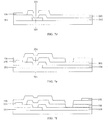
FIG. 1 is a flow diagram of a manufacturing method of an array substrate provided by Embodiment I of the present invention; -
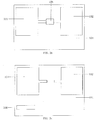
FIGs. 2a to 2f are plan views of the array substrate formed in Embodiment I; -
FIGs. 3a to 3f are sectional views corresponding to the plan views illustrated byFIGs. 2a to 2f ; -
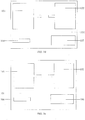
FIGs. 4a to 4f are plan views of an array substrate formed in Embodiment II; -
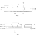
FIGs. 5a to 5f are sectional views corresponding to the plan views illustrated byFIGs. 4a to 4f ; -
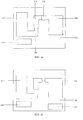
FIGs. 6a to 6f are plan views of an array substrate formed in Embodiment IV; and -
FIGs. 7a to 7f are sectional views corresponding to the plan views illustrated byFIGs. 6a to 6f . - In order to clearly illustrate purposes, technical solutions and advantages of the embodiments of the disclosure, the technical solutions of the embodiments of the present invention will be described in a clearly and fully understandable way in connection with the drawings in the embodiments of the present invention. It is obvious that the described embodiments are just a part but not all of the embodiments of the present invention. Based on the described embodiments herein, those skilled in the art can obtain other embodiment(s), without any inventive work, which should be within the scope of the present invention.
- In order to make those skilled in the art better understand the technical solutions of the embodiments of the present invention, an array substrate and a manufacturing method thereof, a display panel and a display device provided by the embodiments of the present invention will be described in detail in connection with the drawings. The embodiments of the present invention only describe an array substrate in an HADS mode, but array substrates in other display modes, such as, a TN mode, a VA mode or an IPS mode are also within the scope of the present invention. In addition, the present invention only describes an HADS 5 Mask process, but an HADS 4 Mask process or other preparation processes related to the present invention are also within the scope of the present invention.
-
FIG. 1 is a flow diagram of a manufacturing method of an array substrate provided by Embodiment I of the present invention. As illustrated inFIG. 1 , the manufacturing method of the array substrate includes: - Step 1001: forming a first conductive pattern, a second conductive pattern and a metal connection line on a
base substrate 100, the metal connection line being connected with the first conductive pattern and the second conductive pattern. - In the embodiment, the first conductive pattern includes a first gate electrode metal pattern, the second conductive pattern includes a second gate electrode metal pattern, and the gate electrode metal pattern includes a gate electrode and a gate line.
-
FIGs. 2a to 2f are plan views of the array substrate formed by Embodiment I, andFIGs. 3a to 3f are sectional views corresponding to the plan views illustrated byFIGs. 2a to 2f . As illustrated inFIGs. 2a to 2f andFIGs. 3a to 3f , the first gateelectrode metal pattern 101, the second gateelectrode metal pattern 102 and themetal connection line 103 are formed on thebase substrate 100, and themetal connection line 103 is connected with the first gateelectrode metal pattern 101 and the second gateelectrode metal pattern 102. Themetal connection line 103 provided by the embodiment is connected with the first gateelectrode metal pattern 101 and the second gateelectrode metal pattern 102 to make a voltage of the first gateelectrode metal pattern 101 and a voltage of the second gateelectrode metal pattern 102 in a technological process kept to be the same, and therefore an electric potential difference between the first gateelectrode metal pattern 101 and the second gateelectrode metal pattern 102 can be balanced, an electrostatic discharge phenomenon is avoided, finally, endurance capacity of a product on the electrostatic discharge phenomenon is improved, and a product yield is increased. - In the embodiment, a gate insulating layer and an
active layer 104 are formed above the first gateelectrode metal pattern 101, the second gateelectrode metal pattern 102 and themetal connection line 103. What needs to be explained is that, because the gate insulating layer and theactive layer 104 are formed by a single patterning process, in order to facilitate description, the gate insulating layer is not indicated inFIGs. 2a to 2f andFIGS. 3a to 3f . Afirst via hole 105 corresponding to themeal connection line 103 is opened in the gate insulating layer and theactive layer 104, and themetal connection line 103 is exposed through thefirst via hole 105. - Step 1002: etching the metal connection line to make the first conductive pattern and the second conductive pattern insulated from each other.
- In the embodiment, a transparent electrode thin film is formed above the
active layer 104, the transparent electrode thin film and themetal connection line 103 are etched to form a firsttransparent electrode 106. Exemplarily, an etching process comprises wet etching. In the embodiment, themetal connection line 103 is removed through the etching process to make the first gateelectrode metal pattern 101 and the second gateelectrode metal pattern 102 disconnected, therefore avoiding influence on work performance of the first gateelectrode metal pattern 101 and work performance of the second gateelectrode metal pattern 102. - In the embodiment, a source electrode metal pattern and a drain electrode metal pattern are formed above the
active layer 104, the source electrode metal pattern includes a source electrode and a data line, and the drain electrode metal pattern includes a drain electrode. In the embodiment, the source electrode metal pattern and the drain electrode metal pattern are jointly called a source and drain electrode metal pattern. Apassivation layer 108 is formed above a source and drainelectrode metal pattern 107 and the firsttransparent electrode 106, a secondtransparent electrode 109 is formed above thepassivation layer 108. In the firsttransparent electrode 106 and the secondtransparent electrode 109, what is connected with the drain electrode is a pixel electrode, and the other is a common electrode. - The manufacturing method of the array substrate provided by the embodiment comprises: forming the first conductive pattern, the second conductive pattern and the metal connection line on the base substrate, the metal connection line being connected with the first conductive pattern and the second conductive pattern; and etching the metal connection line to make the first conductive pattern and the second conductive pattern insulated from each other. The metal connection line provided by the embodiment is connected with the first conductive pattern and the second conductive pattern to make voltage of the first conductive con pattern and voltage of the second conductive pattern in the technological process kept to be the same, and therefore an electric potential difference between the first conductive pattern and the second conductive pattern can be balanced, the electrostatic discharge phenomenon is avoided, finally, the endurance capacity of the product on the electrostatic discharge phenomenon is improved, and the product yield is increased. In addition, in the embodiment, the metal connection line is removed through the etching process to make the first conductive pattern and the second conductive pattern insulated from each other, therefore avoiding influence on work performance of the first conductive pattern and work performance of the second conductive pattern.
- The embodiment provides a manufacturing method of an array substrate. Referring to
FIG. 1 , the manufacturing method comprises: - Step 1001: forming a first conductive pattern, a second conductive pattern and a metal connection line on a base substrate, the metal connection line being connected with the first conductive pattern and the second conductive pattern.
- In the embodiment, the first conductive pattern includes a first gate electrode metal pattern, the second conductive pattern includes a second gate electrode metal pattern, and the gate electrode metal pattern includes a gate electrode and a gate line.
-
FIGs. 4a to 4f are plan views of the array substrate formed in Embodiment II, andFIGs. 5a to 5f are sectional views corresponding to the plan views illustrated byFIGs. 4a to 4f . As illustrated inFIGs. 4a to 4f andFIGs. 5a to 5f , the first gateelectrode metal pattern 101, the second gateelectrode metal pattern 102 and themetal connection line 103 are formed on the base substrate, and themetal connection line 103 is connected with the first gateelectrode metal pattern 101 and the second gateelectrode metal pattern 102. Themetal connection line 103 provided by the embodiment is connected with the first gateelectrode metal pattern 101 and the second gateelectrode metal pattern 102 to make a voltage of the first gateelectrode metal pattern 101 and a voltage of the second gateelectrode metal pattern 102 in a technological process kept to be the same, and therefore an electric potential difference between the first gateelectrode metal pattern 101 and the second gateelectrode metal pattern 102 can be balanced, an electrostatic discharge phenomenon is avoided, finally, endurance capacity of a product on the electrostatic discharge phenomenon is improved, and a product yield is increased. - In the embodiment, a gate insulating layer and an
active layer 104 are formed above the first gateelectrode metal pattern 101, the second gateelectrode metal pattern 102 and themetal connection line 103. What needs to be explained is that, because the gate insulating layer and theactive layer 104 are formed by a single patterning process, in order to facilitate description, the gate insulating layer is not indicated inFIGs. 4a to 4f andFIGs. 5a to 5f . - Step 1002: etching the metal connection line to make the first conductive pattern and the second conductive pattern insulated from each other.
- In the embodiment, a
transparent electrode 106 is formed above theactive layer 104. A source electrode metal pattern and a drain electrode metal pattern are formed above theactive layer 104, the source electrode metal pattern includes a source electrode and a data line, and the drain electrode metal pattern includes a drain electrode. In the embodiment, the source electrode metal pattern and the drain electrode metal pattern are jointly called a source and drain electrode metal pattern. Apassivation layer 108 is formed above the source and drainelectrode metal pattern 107 and the firsttransparent electrode 106, a first viahole 105 corresponding to themeal connection line 103 is opened in thepassivation layer 108, and themetal connection line 103 is exposed through the first viahole 105. - Exemplarily, a via hole corresponding to the first via hole is further formed in the active layer 4, and therefore the
metal connection line 103 can be exposed. - In the embodiment, a transparent electrode thin film is formed above the
passivation layer 108, the transparent electrode thin film and themetal connection line 103 are etched to form a secondtransparent electrode 109. Exemplarily, an etching process comprises wet etching. In the embodiment, themetal connection line 103 is removed through the etching process to make the first gateelectrode metal pattern 101 and the second gateelectrode metal pattern 102 disconnected, therefore avoiding influence on work performance of the first gateelectrode metal pattern 101 and work performance of the second gateelectrode metal pattern 102. In addition, in the firsttransparent electrode 106 and the secondtransparent electrode 109, what is connected with the drain electrode is a pixel electrode, and the other is a common electrode. - The manufacturing method of the array substrate provided by the embodiment comprises: forming the first conductive pattern, the second conductive pattern and the metal connection line on the base substrate, the metal connection line being connected with the first conductive pattern and the second conductive pattern; and etching the metal connection line to make the first conductive pattern and the second conductive pattern insulated from each other. The metal connection line provided by the embodiment is connected with the first conductive pattern and the second conductive pattern to make a voltage of the first conductive pattern and a voltage of the second conductive pattern in the technological process kept to be the same, and therefore an electric potential difference between the first conductive pattern and the second conductive pattern can be balanced, the electrostatic discharge phenomenon is avoided, finally, the endurance capacity of the product on the electrostatic discharge phenomenon is improved, and the product yield is increased. In addition, in the embodiment, the metal connection line is removed through the etching process to make the first conductive pattern and the second conductive pattern insulated from each other, therefore avoiding influence on work performance of the first conductive pattern and work performance of the second conductive pattern.
- The embodiment provides a manufacturing method of an array substrate. Referring to
FIG. 1 , the manufacturing method comprises: - Step 1001: forming a first conductive pattern, a second conductive pattern and a metal connection line on a base substrate, the metal connection line being connected with the first conductive pattern and the second conductive pattern.
- In the embodiment, the first conductive pattern includes a source electrode metal pattern, the second conductive pattern includes a drain electrode metal pattern, the source electrode metal pattern includes a source electrode and a data line, and the drain electrode metal pattern includes a drain electrode.
- In the embodiment, a gate electrode metal pattern is formed on the base substrate and includes a gate electrode and a gate line. A gate insulating layer and an active layer are formed above the gate electrode metal pattern, and a first transparent electrode is formed above the active layer. The source electrode metal pattern, the drain electrode metal pattern and the metal connection line are formed above the active layer, and the metal connection line is connected with the source electrode metal pattern and the drain electrode metal pattern. The metal connection line provided by the embodiment is connected with the source electrode metal pattern and the drain electrode metal pattern to make a voltage of the source electrode metal pattern and a voltage of the drain electrode metal pattern in a technological process kept to be the same, and therefore an electric potential difference between the source electrode metal pattern and the drain electrode metal pattern can be balanced, an electrostatic discharge phenomenon is avoided, finally, endurance capacity of a product on the electrostatic discharge phenomenon is improved, and a product yield is increased.
- Step 1002: etching the metal connection line to make the first conductive pattern and the second conductive pattern insulated from each other.
- A passivation layer is formed above the source electrode metal pattern, the drain electrode metal pattern and the first transparent electrode, a first via hole corresponding to the metal connection line is formed in the passivation layer, and the metal connection line is exposed through the first via hole.
- In the embodiment, a transparent electrode thin film is formed above the passivation layer, and the transparent electrode thin film and the metal connection line are etched to form a second transparent electrode. In the embodiment, the metal connection line is removed through an etching process to make the source electrode metal pattern and the drain electrode metal pattern disconnected, therefore avoiding influence on work performance of the source electrode metal pattern and work performance of the drain electrode metal pattern. In addition, in the first transparent electrode and the second transparent electrode, what is connected with the drain electrode is a pixel electrode, and the other is a common electrode.
- The manufacturing method of the array substrate provided by the embodiment comprises: forming the first conductive pattern, the second conductive pattern and the metal connection line on the base substrate, the metal connection line being connected with the first conductive pattern and the second conductive pattern; and etching the metal connection line to make the first conductive pattern and the second conductive pattern insulated from each other. The metal connection line provided by the embodiment is connected with the first conductive pattern and the second conductive pattern to make a voltage of the first conductive pattern and a voltage of the second conductive pattern in the technological process kept to be the same, and therefore an electric potential difference between the first conductive pattern and the second conductive pattern can be balanced, the electrostatic discharge phenomenon is avoided, finally, the endurance capacity of the product on the electrostatic discharge phenomenon is improved, and the product yield is increased. In addition, in the embodiment, the metal connection line is removed through the etching process to make the first conductive pattern and the second conductive pattern insulated from each other, therefore avoiding influence on work performance of the first conductive pattern and work performance of the second conductive pattern.
- The embodiment provides a manufacturing method of an array substrate. Referring to
FIG. 1 , the manufacturing method comprises: - Step 1001: forming a first conductive pattern, a second conductive pattern and a metal connection line on a base substrate, the metal connection line being connected with the first conductive pattern and the second conductive pattern.
- In the embodiment, the metal connection line includes a first sub-connection line and a second sub-connection line which are connected with each other, the first sub-connection line is connected with the first conductive pattern, the second sub-connection line is connected with the second conductive pattern, the first conductive pattern includes a gate electrode metal pattern, and the second conductive pattern includes a source electrode metal pattern or a drain electrode metal pattern. The second conductive pattern provided by the embodiment is the source electrode metal pattern, and regarding the content that the second conductive pattern is the drain electrode metal pattern, please refer to Embodiment V. The gate electrode metal pattern includes a gate electrode and a gate line, the source electrode metal pattern includes a source electrode and a data line, and the drain electrode metal pattern includes a drain electrode.
-
FIGs. 6a to 6f are plan views of the array substrate formed in Embodiment IV andFIGs. 7a to 7f are sectional views corresponding to the plan views illustrated byFIGs. 6a to 6f . As illustrated inFIGs. 6a to 6f andFIGs. 7a to 7f , the gateelectrode metal pattern 201 and the firstsub-connection line 202 are formed on the base substrate, and the firstsub-connection line 202 is connected with the gateelectrode metal pattern 201. A gate insulating layer and an active layer are formed above the gateelectrode metal pattern 201 and the firstsub-connection line 202. What needs to be explained is that, because the gate insulating layer and the active layer are formed by a single patterning process, in order to facilitate description, the gate insulating layer is not indicated inFIGs. 6a to 6f andFIGs. 7a to 7f . A second viahole 203 corresponding to the firstsub-connection line 202 is opened in the gate insulating layer and the active layer, and the firstsub-connection line 202 is exposed through the second viahole 203. - In the embodiment, a first
transparent electrode 106 is formed above theactive layer 104, the source electrode metal pattern, the drain electrode metal pattern and thesecond sub-connection wire 204 are formed above theactive layer 104. What needs to be explained is that, because the source electrode metal pattern and the drain electrode metal pattern are formed by a single patterning process, in order to facilitate description, the drain electrode metal pattern is not indicated inFIGs. 6a to 6f andFIGs. 7a to 7f . Thesecond sub-connection wire 204 is connected with the sourceelectrode metal pattern 205 and connected with the firstsub-connection line 202 through the second viahole 203, the source electrode metal pattern includes the source electrode and the data line, and the drain electrode metal pattern includes the drain electrode. The firstsub-connection line 202 and thesecond sub-connection wire 204 provided by the embodiment are connected with the gateelectrode metal pattern 201 and the sourceelectrode metal pattern 205 to make a voltage of the gateelectrode metal pattern 201 and a voltage of the sourceelectrode metal pattern 205 in a technological process kept to be the same, and therefore an electric potential difference between the gateelectrode metal pattern 201 and the sourceelectrode metal pattern 205 can be balanced, an electrostatic discharge phenomenon is avoided, finally, the endurance capacity of the product on the electrostatic discharge phenomenon is improved, and the product yield is increased. - Step 1002: etching the metal connection line to make the first conductive pattern and the second conductive pattern insulated from each other.
- In the embodiment, a
passivation layer 108 is formed above the sourceelectrode metal pattern 205 and the firsttransparent electrode 106, a first viahole 105 corresponding to the secondsub-connection line 204 is formed in thepassivation layer 108, and the secondsub-connection line 204 is exposed through the first viahole 105. Of course, a first viahole 105 corresponding to the firstsub-connection line 202 can also be formed in thepassivation layer 108. - In the embodiment, a transparent electrode thin film is formed above the
passivation layer 108, the transparent electrode thin film and the secondsub-connection line 204 are etched to form a secondtransparent electrode 109. In the embodiment, part or all of the secondsub-connection line 204 is removed by an etching process, so that the gateelectrode metal pattern 201 and the sourceelectrode metal pattern 205 can be disconnected, therefore avoiding influence on work performance of the gateelectrode metal pattern 201 and work performance of the sourceelectrode metal pattern 205. In addition, in the firsttransparent electrode 106 and the secondtransparent electrode 109, what is connected with the drain electrode is a pixel electrode, and the other is a common electrode. - The manufacturing method of the array substrate provided by the embodiment comprises: forming the first conductive pattern, the second conductive pattern and the metal connection line on the base substrate, the metal connection line being connected with the first conductive pattern and the second conductive pattern; and etching the metal connection line to make the first conductive pattern and the second conductive pattern insulated from each other. The metal connection line provided by the embodiment is connected with the first conductive pattern and the second conductive pattern to make a voltage of the first conductive pattern and a voltage of the second conductive pattern in the technological process kept to be the same, and therefore an electric potential difference between the first conductive pattern and the second conductive pattern can be balanced, the electrostatic discharge phenomenon is avoided, finally, the endurance capacity of the product on the electrostatic discharge phenomenon is improved, and the product yield is increased. In addition, in the embodiment, the metal connection line is removed through the etching process to make the first conductive pattern and the second conductive pattern insulated from each other, therefore avoiding influence on work performance of the first conductive pattern and work performance of the second conductive pattern.
- The embodiment provides a manufacturing method of an array substrate. Referring to
FIG. 1 , the manufacturing method comprises: - Step 1001: forming a first conductive pattern, a second conductive pattern and a metal connection line on a base substrate, the metal connection line being connected with the first conductive pattern and the second conductive pattern.
- In the embodiment, the metal connection line includes a first sub-connection line and a second sub-connection line which are connected with each other, the first sub-connection line is connected with the first conductive pattern, the second sub-connection line is connected with the second conductive pattern, the first conductive pattern includes a gate electrode metal pattern, the second conductive pattern includes a drain electrode metal pattern, the gate electrode metal pattern includes a gate electrode and a gate line, a source electrode metal pattern includes a source electrode and a data line, and the drain electrode metal pattern includes a drain electrode.
- Step 1002: etching the metal connection line to make the first conductive pattern and the second conductive pattern insulated from each other.
- A difference between the manufacturing method provided by the embodiment and the manufacturing method provided by the above Embodiment IV lies in that the second sub-connection line in the embodiment is connected with the drain electrode metal pattern, while the second sub-connection line in the above Embodiment IV is connected with the source electrode metal pattern; and the rest are completely same. Thus, detailed content can refer to description of the above Embodiment IV and will not be repeated herein.
- The manufacturing method of the array substrate provided by the embodiment comprises: forming the first conductive pattern, the second conductive pattern and the metal connection line on the base substrate, the metal connection line being connected with the first conductive pattern and the second conductive pattern; and etching the metal connection line to make the first conductive pattern and the second conductive pattern insulated from each other. The metal connection line provided by the embodiment is connected with the first conductive pattern and the second conductive pattern to make a voltage of the first conductive pattern and a voltage of the second conductive pattern in a technological process kept to be the same, and therefore an electric potential difference between the first conductive pattern and the second conductive pattern can be balanced, an electrostatic discharge phenomenon is avoided, finally, endurance capacity of a product on the electrostatic discharge phenomenon is improved, and a product yield is increased. In addition, in the embodiment, the metal connection line is removed through an etching process to make the first conductive pattern and the second conductive pattern insulated from each other, therefore avoiding influence on work performance of the first conductive pattern and work performance of the second conductive pattern.
- The embodiment provides an array substrate, which is prepared according to any one of the methods in Embodiment I to Embodiment V, detailed content of a manufacturing method of the array substrate can refer to description of Embodiment I to Embodiment V and will not be repeated herein.
- In the array substrate provided by the embodiment, the manufacturing method of the array substrate comprises: forming the first conductive pattern, the second conductive pattern and the metal connection line on the base substrate, the metal connection line being connected with the first conductive pattern and the second conductive pattern; and etching the metal connection line to make the first conductive pattern and the second conductive pattern insulated from each other. The metal connection line provided by the embodiment is connected with the first conductive pattern and the second conductive pattern to make a voltage of the first conductive pattern and a voltage of the second conductive pattern in a technological process kept to be the same, and therefore an electric potential difference between the first conductive pattern and the second conductive pattern can be balanced, an electrostatic discharge phenomenon is avoided, finally, endurance capacity of a product on the electrostatic discharge phenomenon is improved, and a product yield is increased. In addition, in the embodiment, the metal connection line is removed through an etching process to make the first conductive pattern and the second conductive pattern insulated from each other, therefore avoiding influence on work performance of the first conductive pattern and work performance of the second conductive pattern.
- The embodiment provides a display substrate, comprising: the array substrate provided by the above Embodiment VI and a substrate opposite to the array substrate, and detailed content can refer to description of the above Embodiment VI and will not be repeated herein.
- In the display panel provided with the embodiment, a manufacturing method of the array substrate comprises: forming a first conductive pattern, a second conductive pattern and a metal connection line on a base substrate, the metal connection line being connected with the first conductive pattern and the second conductive pattern; and etching the metal connection line to make the first conductive pattern and the second conductive pattern insulated from each other. The metal connection line provided by the embodiment is connected with the first conductive pattern and the second conductive pattern to make a voltage of the first conductive pattern and a voltage of the second conductive pattern in a technological process kept to be the same, and therefore an electric potential difference between the first conductive pattern and the second conductive pattern can be balanced, an electrostatic discharge phenomenon is avoided, finally, endurance capacity of a product on the electrostatic discharge phenomenon is improved, and a product yield is increased. In addition, in the embodiment, the metal connection line is removed through an etching process to make the first conductive pattern and the second conductive pattern insulated from each other, therefore avoiding influence on work performance of the first conductive pattern and work performance of the second conductive pattern.
- The embodiment provides a display device, comprising the display panel provided by the above Embodiment VII, and detailed content can refer to description of the above Embodiment VII and will not be repeated herein.
- In the display device provided by the embodiment, a manufacturing method of an array substrate comprises: forming a first conductive pattern, a second conductive pattern and a metal connection line on a base substrate, the metal connection line being connected with the first conductive pattern and the second conductive pattern; and etching the metal connection line to make the first conductive pattern and the second conductive pattern insulated from each other. The metal connection line provided by the embodiment is connected with the first conductive pattern and the second conductive pattern to make a voltage of the first conductive pattern and a voltage of the second conductive pattern in a technological process kept to be the same, and therefore an electric potential difference between the first conductive pattern and the second conductive pattern can be balanced, an electrostatic discharge phenomenon is avoided, finally, endurance capacity of a product on the electrostatic discharge phenomenon is improved, and a product yield is increased. In addition, in the embodiment, the metal connection line is removed through an etching process to make the first conductive pattern and the second conductive pattern insulated from each other, therefore avoiding influence on work performance of the first conductive pattern and work performance of the second conductive pattern.
- In the array substrate and the manufacturing method of thereof, the display panel and the display device provided by the embodiments of the present invention, the manufacturing method comprises: forming a first conductive pattern, a second conductive pattern and a metal connection line on a base substrate, the metal connection line being connected with the first conductive pattern and the second conductive pattern; and etching the metal connection line to make the first conductive pattern and the second conductive pattern insulated from each other. The metal connection line provided by the embodiment is connected with the first conductive pattern and the second conductive pattern to make a voltage of the first conductive pattern and a voltage of the second conductive pattern in a technological process kept to be the same, and therefore an electric potential difference between the first conductive pattern and the second conductive pattern can be balanced, an electrostatic discharge phenomenon is avoided, finally, endurance capacity of a product on the electrostatic discharge phenomenon is improved, and a product yield is increased. In addition, in the embodiment, the metal connection line is removed through an etching process to make the first conductive pattern and the second conductive pattern insulated from each other, therefore avoiding influence on work performance of the first conductive pattern and work performance of the second conductive pattern.
- What can be understood is that, the foregoing embodiments merely are exemplary embodiments of the disclosure in order to illustrate the principle of the embodiment, and not intended to define the scope of the disclosure. Those skilled in the art can make various changes and improvements without departing from the spirit of the disclosure, and all such changes and improvements are within the scope of the claims of the disclosure.
- The present application claims priority of Chinese Patent Application No.
201510369478.6 filed on June 26, 2015
Claims (18)
- A manufacturing method of an array substrate, comprising:forming a first conductive pattern, a second conductive pattern and a metal connection line on a base substrate, the metal connection line being connected with the first conductive pattern and the second conductive pattern; andetching the metal connection line to make the first conductive pattern and the second conductive pattern insulated from each other.
- The manufacturing method of the array substrate according to claim 1, wherein, the first conductive pattern includes a first gate electrode metal pattern, the second conductive pattern includes a second gate electrode metal pattern, and the gate electrode metal pattern includes a gate electrode and a gate line.
- The manufacturing method of the array substrate according to claim 2, wherein, the first conductive pattern is a first gate electrode metal pattern, the second conductive pattern is a second gate electrode metal pattern, and the gate electrode metal pattern includes a gate electrode and a gate line.
- The manufacturing method of the array substrate according to claim 3, wherein, forming the first conductive pattern, the second conductive pattern and the metal connection line on the base substrate includes:forming the first gate electrode metal pattern, the second gate electrode metal pattern and the metal connection line on the base substrate, the metal connection line being connected with the first gate electrode metal pattern and the second gate electrode metal pattern,after forming the first gate electrode metal pattern, the second gate electrode metal pattern and the metal connection line on the base substrate and before etching the metal connection line to make the first conductive pattern and the second conductive pattern insulated from each other, the method includes:forming a gate insulating layer and an active layer on the first gate electrode metal pattern, the second gate electrode metal pattern and the metal connection line, and forming a first via hole corresponding to the meal connection line in the gate insulating layer and the active layer,etching the metal connection line to make the first conductive pattern and the second conductive pattern insulated from each other includes:forming a transparent electrode thin film above the active layer;etching the transparent electrode thin film and the metal connection line to form a first transparent electrode.
- The manufacturing method of the array substrate according to claim 3, wherein, forming the first conductive pattern, the second conductive pattern and the metal connection line on the base substrate includes:forming the first gate electrode metal pattern, the second gate electrode metal pattern and the metal connection line on the base substrate, the metal connection line being connected with the first gate electrode metal pattern and the second gate electrode metal pattern,after forming the first gate electrode metal pattern, the second gate electrode metal pattern and the metal connection line on the base substrate and before etching the metal connection line to make the first conductive pattern and the second conductive pattern insulated from each other, the method includes:forming a passivation layer above the first gate electrode metal pattern, the second gate electrode metal pattern and the metal connection line, and forming a first via hole corresponding to the meal connection line in the passivation layer,etching the metal connection line to make the first conductive pattern and the second conductive pattern insulated from each other includes:forming a transparent electrode thin film above the passivation layer;etching the transparent electrode thin film and the metal connection line to form a second transparent electrode.
- The manufacturing method of the array substrate according to claim 5, wherein, before forming the passivation layer above the first gate electrode metal pattern, the second gate electrode metal pattern and the metal connection line and after forming the first conductive pattern, the second conductive pattern and the metal connection line on the base substrate, the method further includes:forming a gate insulating layer and an active layer above the first gate electrode metal pattern, the second gate electrode metal pattern and the metal connection line;forming a first transparent electrode, a source electrode metal pattern and a drain electrode metal pattern above the gate insulating layer and the active layer.
- The manufacturing method of the array substrate according to claim 6, wherein, forming the passivation layer above the first gate electrode metal pattern, the second gate electrode metal pattern and the metal connection line includes:forming the passivation layer on the base substrate where the first transparent electrode, the source electrode metal pattern and the drain electrode metal pattern are formed.
- The manufacturing method of the array substrate according to claim 6, comprising:forming a via hole corresponding to the metal connection line and the first via hole in layers where the gate insulating layer and the active layer are located simultaneously with forming the first via hole corresponding to the metal connection line in the passivation layer.
- The manufacturing method of the array substrate according to claim 1, wherein, the first conductive pattern includes a source electrode metal pattern, the second conductive pattern includes a drain electrode metal pattern, the source electrode metal pattern includes a source electrode and a data line, and the drain electrode metal pattern includes a drain electrode.
- The manufacturing method of the array substrate according to claim 9, wherein, forming the first conductive pattern, the second conductive pattern and the metal connection line on the base substrate includes:forming the source electrode metal pattern, the drain electrode metal pattern and the metal connection line on the base substrate, the metal connection line being connected with the source electrode metal pattern and the drain electrode metal pattern;after forming the source electrode metal pattern, the drain electrode metal pattern and the metal connection line on the base substrate and before etching the metal connection line to make the first conductive pattern and the second conductive pattern insulated from each other, the method includes:forming a passivation layer above the source electrode metal pattern, the drain electrode metal pattern and the metal connection line, and forming a first via hole corresponding to the metal connection line in the passivation layer;etching the metal connection line to make the first conductive pattern and the second conductive pattern insulated from each other includes:forming a transparent electrode thin film above the passivation layer;etching the transparent electrode thin film and the metal connection line to form a second transparent electrode.
- The manufacturing method of the array substrate according to claim 1, wherein, the metal connection line includes a first sub-connection line and a second sub-connection line which are connected with each other, the first sub-connection line is connected with the first conductive pattern, and the second sub-connection line is connected with the second conductive pattern.
- The manufacturing method of the array substrate according to claim 11, wherein, the first conductive pattern includes a gate electrode metal pattern, the second conductive pattern includes a source electrode metal pattern or a drain electrode metal pattern, the gate electrode metal pattern includes a gate electrode and a gate line, the source electrode metal pattern includes a source electrode and a data line, and the drain electrode metal pattern includes a drain electrode.
- The manufacturing method of the array substrate according to claim 12, wherein, forming the first conductive pattern, the second conductive pattern and the metal connection line on the base substrate includes:forming the gate electrode metal pattern and the first sub-connection line on the base substrate, the first sub-connection line being connected with the gate electrode metal pattern;forming a gate insulating layer and an active layer above the gate electrode metal pattern and the first sub-connection line, and forming a second via hole corresponding to the first sub-connection line in the gate insulating layer and the active layer;forming the source electrode metal pattern, the drain electrode metal pattern and the second sub-connection line above the gate insulating layer and the active layer, the second sub-connection line being connected with the source electrode metal pattern, and the second sub-connection line being connected with the first sub-connection line through the second via hole;before etching the metal connection line to make the first conductive pattern and the second conductive pattern insulated from each other and after forming the first conductive pattern, the second conductive pattern and the metal connection line on the base substrate, the method includes:forming a passivation layer above the source electrode metal pattern, the drain electrode metal pattern and the second sub-connection line, and forming a first via hole corresponding to the first sub-connection line or the second sub-connection line in the passivation layer;etching the metal connection line to make the first conductive pattern and the second conductive pattern insulated from each other includes:forming a transparent electrode thin film above the passivation layer;etching the transparent electrode thin film and the first sub-connection line or the second sub-connection line through the first via hole to form a second transparent electrode.
- The manufacturing method of the array substrate according to claim 12, wherein, forming the first conductive pattern, the second conductive pattern and the metal connection line on the base substrate includes:forming the gate electrode metal pattern and the first sub-connection line on the base substrate, the first sub-connection line being connected with the gate electrode metal pattern;forming a gate insulating layer and an active layer above the gate electrode metal pattern and the first sub-connection line, and forming a second via hole corresponding to the first sub-connection line in the gate insulating layer and the active layer;forming the source electrode metal pattern, the drain electrode metal pattern and the second sub-connection line above the gate insulating layer and the active layer, the second sub-connection line being connected with the drain electrode metal pattern, and the second sub-connection line being connected with the first sub-connection line through the second via hole;before etching the metal connection line to make the first conductive pattern and the second conductive pattern insulated from each other and after forming the first conductive pattern, the second conductive pattern and the metal connection line on the base substrate, the method includes:forming a passivation layer above the source electrode metal pattern, the drain electrode metal pattern and the second sub-connection line, and forming a first via hole corresponding to the first sub-connection line or the second sub-connection line in the passivation layer;etching the metal connection line to make the first conductive pattern and the second conductive pattern insulated from each other includes:forming a transparent electrode thin film above the passivation layer;etching the transparent electrode thin film and the first sub-connection line or the second sub-connection line through the first via hole to form a second transparent electrode.
- The manufacturing method of the array substrate according to any one of claims 1 to 14, wherein the etching includes wet etching.
- An array substrate, manufactured by using the manufacturing method of the array substrate according to any one of claims 1 to 15.
- A display panel, comprising:the array substrate according to claim 16; andan opposed substrate, arranged opposite to the array substrate.
- A display device, comprising the display panel according to claim 17.
Applications Claiming Priority (2)
| Application Number | Priority Date | Filing Date | Title |
|---|---|---|---|
| CN201510369478.6A CN105185740B (en) | 2015-06-26 | 2015-06-26 | A kind of array substrate and preparation method thereof, display panel and display device |
| PCT/CN2015/093387 WO2016206268A1 (en) | 2015-06-26 | 2015-10-30 | Matrix panel and manufacturing method thereof, and display panel and display device |
Publications (3)
| Publication Number | Publication Date |
|---|---|
| EP3316284A1 true EP3316284A1 (en) | 2018-05-02 |
| EP3316284A4 EP3316284A4 (en) | 2019-02-20 |
| EP3316284B1 EP3316284B1 (en) | 2022-05-18 |
Family
ID=54907732
Family Applications (1)
| Application Number | Title | Priority Date | Filing Date |
|---|---|---|---|
| EP15892061.1A Active EP3316284B1 (en) | 2015-06-26 | 2015-10-30 | Manufacturing method for a matrix panel of a display device |
Country Status (4)
| Country | Link |
|---|---|
| US (1) | US20180226476A1 (en) |
| EP (1) | EP3316284B1 (en) |
| CN (1) | CN105185740B (en) |
| WO (1) | WO2016206268A1 (en) |
Families Citing this family (2)
| Publication number | Priority date | Publication date | Assignee | Title |
|---|---|---|---|---|
| CN106206607B (en) * | 2016-08-08 | 2019-12-10 | 京东方科技集团股份有限公司 | Manufacturing method of array substrate, array substrate and display panel |
| CN111430302A (en) * | 2020-04-02 | 2020-07-17 | 合肥鑫晟光电科技有限公司 | Array substrate, manufacturing method thereof and display device |
Family Cites Families (12)
| Publication number | Priority date | Publication date | Assignee | Title |
|---|---|---|---|---|
| US582435A (en) * | 1897-05-11 | Truck for railway-cars | ||
| JP3642876B2 (en) * | 1995-08-04 | 2005-04-27 | 株式会社半導体エネルギー研究所 | Method for manufacturing semiconductor device using plasma and semiconductor device manufactured using plasma |
| JP4790166B2 (en) * | 2001-07-05 | 2011-10-12 | Okiセミコンダクタ株式会社 | Protection transistor |
| JP4319517B2 (en) * | 2003-10-28 | 2009-08-26 | 東芝モバイルディスプレイ株式会社 | Array substrate and flat display device |
| TWI255959B (en) * | 2004-02-23 | 2006-06-01 | Toppoly Optoelectronics Corp | Method of manufacturing thin film transistor array |
| US7768590B2 (en) * | 2005-04-26 | 2010-08-03 | Sharp Kabushiki Kaisha | Production method of active matrix substrate, active matrix substrate, and liquid crystal display device |
| US8716605B2 (en) * | 2010-10-22 | 2014-05-06 | Lg Display Co., Ltd. | Structure for shorting line connecting signal lines of flat panel display device |
| CN102540524B (en) * | 2010-12-30 | 2015-10-07 | 北京京东方光电科技有限公司 | Prevent the method for electrostatic breakdown, the manufacture method of array base palte and display backboard |
| CN102945846B (en) * | 2012-09-28 | 2016-03-30 | 京东方科技集团股份有限公司 | Array base palte and manufacture method, display unit |
| CN104392990B (en) * | 2014-11-25 | 2018-07-13 | 合肥鑫晟光电科技有限公司 | A kind of array substrate and display device |
| CN104658973B (en) * | 2015-02-28 | 2017-10-24 | 京东方科技集团股份有限公司 | Array base palte and preparation method thereof, display device |
| JP6832624B2 (en) * | 2015-12-22 | 2021-02-24 | 三菱電機株式会社 | Liquid crystal display device and its manufacturing method |
-
2015
- 2015-06-26 CN CN201510369478.6A patent/CN105185740B/en active Active
- 2015-10-30 EP EP15892061.1A patent/EP3316284B1/en active Active
- 2015-10-30 US US15/325,597 patent/US20180226476A1/en not_active Abandoned
- 2015-10-30 WO PCT/CN2015/093387 patent/WO2016206268A1/en not_active Ceased
Also Published As
| Publication number | Publication date |
|---|---|
| EP3316284A4 (en) | 2019-02-20 |
| CN105185740A (en) | 2015-12-23 |
| EP3316284B1 (en) | 2022-05-18 |
| US20180226476A1 (en) | 2018-08-09 |
| WO2016206268A1 (en) | 2016-12-29 |
| CN105185740B (en) | 2019-01-15 |
Similar Documents
| Publication | Publication Date | Title |
|---|---|---|
| US10573595B2 (en) | Array substrate, fabricating method thereof, and display device | |
| EP3188235B1 (en) | Array substrate and manufacturing method thereof, display panel and display device | |
| CN103454819B (en) | Array base palte and manufacture method thereof for liquid crystal display | |
| US20190051667A1 (en) | An array substrate and a manufacturing method thereof, a display panel, as well as a display device | |
| CN104900633B (en) | A kind of manufacturing method of array base plate, array base palte and display device | |
| CN209946604U (en) | Array substrate, display panel and display device | |
| US20120168791A1 (en) | Method for preventing electrostatic breakdown, method for manufacturing array substrate and display substrate | |
| CN103296021A (en) | TFT array substrate | |
| CN106932984A (en) | Thin film transistor base plate and its manufacture method | |
| CN105679771A (en) | Array substrate and manufacturing method thereof and display panel comprising array substrate | |
| EP3151279B1 (en) | Array substrate and manufacturing method therefor, and display device | |
| US8861065B2 (en) | Electronic paper active substrate and method of forming the same and electronic paper display panel | |
| US10598995B2 (en) | Array substrate, fabrication method, and corresponding display panel and electronic device | |
| EP3316284A1 (en) | Matrix panel and manufacturing method thereof, and display panel and display device | |
| CN103123428A (en) | Thin film transistor (TFT)-liquid crystal display (LCD) array substrate and production method thereof | |
| CN105676553A (en) | Array substrate, manufacturing method thereof, display panel and display device | |
| US20160276368A1 (en) | Thin-Film Transistor Array Substrate And Method For Manufacturing Thin-Film Transistor Array Substrate | |
| CN108257974A (en) | Array substrate, display device and the method for preparing array substrate | |
| CN108122926A (en) | Array substrate and preparation method thereof, display panel and display device | |
| US10903249B2 (en) | Array substrate and manufacturing method thereof, display device | |
| US10126343B2 (en) | ESD detection method for array substrate | |
| US9618810B2 (en) | Array substrate and liquid crystal display panel | |
| US20170160608A1 (en) | TFT Display Device And The Method For Producing The Same | |
| US10288961B2 (en) | Array substrate and display apparatus | |
| CN105261591B (en) | A kind of array substrate and preparation method thereof, display device |
Legal Events
| Date | Code | Title | Description |
|---|---|---|---|
| STAA | Information on the status of an ep patent application or granted ep patent |
Free format text: STATUS: UNKNOWN |
|
| STAA | Information on the status of an ep patent application or granted ep patent |
Free format text: STATUS: THE INTERNATIONAL PUBLICATION HAS BEEN MADE |
|
| PUAI | Public reference made under article 153(3) epc to a published international application that has entered the european phase |
Free format text: ORIGINAL CODE: 0009012 |
|
| STAA | Information on the status of an ep patent application or granted ep patent |
Free format text: STATUS: REQUEST FOR EXAMINATION WAS MADE |
|
| 17P | Request for examination filed |
Effective date: 20161121 |
|
| AK | Designated contracting states |
Kind code of ref document: A1 Designated state(s): AL AT BE BG CH CY CZ DE DK EE ES FI FR GB GR HR HU IE IS IT LI LT LU LV MC MK MT NL NO PL PT RO RS SE SI SK SM TR |
|
| AX | Request for extension of the european patent |
Extension state: BA ME |
|
| DAV | Request for validation of the european patent (deleted) | ||
| DAX | Request for extension of the european patent (deleted) | ||
| R17P | Request for examination filed (corrected) |
Effective date: 20161121 |
|
| A4 | Supplementary search report drawn up and despatched |
Effective date: 20190117 |
|
| RIC1 | Information provided on ipc code assigned before grant |
Ipc: H01L 29/786 20060101ALI20190111BHEP Ipc: H01L 29/417 20060101ALI20190111BHEP Ipc: H01L 27/02 20060101ALI20190111BHEP Ipc: G02F 1/1362 20060101ALI20190111BHEP Ipc: H01L 21/77 20170101AFI20190111BHEP Ipc: H01L 27/12 20060101ALI20190111BHEP |
|
| STAA | Information on the status of an ep patent application or granted ep patent |
Free format text: STATUS: EXAMINATION IS IN PROGRESS |
|
| 17Q | First examination report despatched |
Effective date: 20200519 |
|
| GRAP | Despatch of communication of intention to grant a patent |
Free format text: ORIGINAL CODE: EPIDOSNIGR1 |
|
| STAA | Information on the status of an ep patent application or granted ep patent |
Free format text: STATUS: GRANT OF PATENT IS INTENDED |
|
| INTG | Intention to grant announced |
Effective date: 20211216 |
|
| GRAS | Grant fee paid |
Free format text: ORIGINAL CODE: EPIDOSNIGR3 |
|
| GRAA | (expected) grant |
Free format text: ORIGINAL CODE: 0009210 |
|
| STAA | Information on the status of an ep patent application or granted ep patent |
Free format text: STATUS: THE PATENT HAS BEEN GRANTED |
|
| AK | Designated contracting states |
Kind code of ref document: B1 Designated state(s): AL AT BE BG CH CY CZ DE DK EE ES FI FR GB GR HR HU IE IS IT LI LT LU LV MC MK MT NL NO PL PT RO RS SE SI SK SM TR |
|
| REG | Reference to a national code |
Ref country code: GB Ref legal event code: FG4D |
|
| REG | Reference to a national code |
Ref country code: CH Ref legal event code: EP |
|
| REG | Reference to a national code |
Ref country code: IE Ref legal event code: FG4D |
|
| REG | Reference to a national code |
Ref country code: DE Ref legal event code: R096 Ref document number: 602015079112 Country of ref document: DE |
|
| REG | Reference to a national code |
Ref country code: AT Ref legal event code: REF Ref document number: 1493629 Country of ref document: AT Kind code of ref document: T Effective date: 20220615 |
|
| REG | Reference to a national code |
Ref country code: LT Ref legal event code: MG9D |
|
| REG | Reference to a national code |
Ref country code: NL Ref legal event code: MP Effective date: 20220518 |
|
| REG | Reference to a national code |
Ref country code: AT Ref legal event code: MK05 Ref document number: 1493629 Country of ref document: AT Kind code of ref document: T Effective date: 20220518 |
|
| PG25 | Lapsed in a contracting state [announced via postgrant information from national office to epo] |
Ref country code: SE Free format text: LAPSE BECAUSE OF FAILURE TO SUBMIT A TRANSLATION OF THE DESCRIPTION OR TO PAY THE FEE WITHIN THE PRESCRIBED TIME-LIMIT Effective date: 20220518 Ref country code: PT Free format text: LAPSE BECAUSE OF FAILURE TO SUBMIT A TRANSLATION OF THE DESCRIPTION OR TO PAY THE FEE WITHIN THE PRESCRIBED TIME-LIMIT Effective date: 20220919 Ref country code: NO Free format text: LAPSE BECAUSE OF FAILURE TO SUBMIT A TRANSLATION OF THE DESCRIPTION OR TO PAY THE FEE WITHIN THE PRESCRIBED TIME-LIMIT Effective date: 20220818 Ref country code: NL Free format text: LAPSE BECAUSE OF FAILURE TO SUBMIT A TRANSLATION OF THE DESCRIPTION OR TO PAY THE FEE WITHIN THE PRESCRIBED TIME-LIMIT Effective date: 20220518 Ref country code: LT Free format text: LAPSE BECAUSE OF FAILURE TO SUBMIT A TRANSLATION OF THE DESCRIPTION OR TO PAY THE FEE WITHIN THE PRESCRIBED TIME-LIMIT Effective date: 20220518 Ref country code: HR Free format text: LAPSE BECAUSE OF FAILURE TO SUBMIT A TRANSLATION OF THE DESCRIPTION OR TO PAY THE FEE WITHIN THE PRESCRIBED TIME-LIMIT Effective date: 20220518 Ref country code: GR Free format text: LAPSE BECAUSE OF FAILURE TO SUBMIT A TRANSLATION OF THE DESCRIPTION OR TO PAY THE FEE WITHIN THE PRESCRIBED TIME-LIMIT Effective date: 20220819 Ref country code: FI Free format text: LAPSE BECAUSE OF FAILURE TO SUBMIT A TRANSLATION OF THE DESCRIPTION OR TO PAY THE FEE WITHIN THE PRESCRIBED TIME-LIMIT Effective date: 20220518 Ref country code: ES Free format text: LAPSE BECAUSE OF FAILURE TO SUBMIT A TRANSLATION OF THE DESCRIPTION OR TO PAY THE FEE WITHIN THE PRESCRIBED TIME-LIMIT Effective date: 20220518 Ref country code: BG Free format text: LAPSE BECAUSE OF FAILURE TO SUBMIT A TRANSLATION OF THE DESCRIPTION OR TO PAY THE FEE WITHIN THE PRESCRIBED TIME-LIMIT Effective date: 20220818 Ref country code: AT Free format text: LAPSE BECAUSE OF FAILURE TO SUBMIT A TRANSLATION OF THE DESCRIPTION OR TO PAY THE FEE WITHIN THE PRESCRIBED TIME-LIMIT Effective date: 20220518 |
|
| PG25 | Lapsed in a contracting state [announced via postgrant information from national office to epo] |
Ref country code: RS Free format text: LAPSE BECAUSE OF FAILURE TO SUBMIT A TRANSLATION OF THE DESCRIPTION OR TO PAY THE FEE WITHIN THE PRESCRIBED TIME-LIMIT Effective date: 20220518 Ref country code: PL Free format text: LAPSE BECAUSE OF FAILURE TO SUBMIT A TRANSLATION OF THE DESCRIPTION OR TO PAY THE FEE WITHIN THE PRESCRIBED TIME-LIMIT Effective date: 20220518 Ref country code: LV Free format text: LAPSE BECAUSE OF FAILURE TO SUBMIT A TRANSLATION OF THE DESCRIPTION OR TO PAY THE FEE WITHIN THE PRESCRIBED TIME-LIMIT Effective date: 20220518 Ref country code: IS Free format text: LAPSE BECAUSE OF FAILURE TO SUBMIT A TRANSLATION OF THE DESCRIPTION OR TO PAY THE FEE WITHIN THE PRESCRIBED TIME-LIMIT Effective date: 20220918 |
|
| PG25 | Lapsed in a contracting state [announced via postgrant information from national office to epo] |
Ref country code: SM Free format text: LAPSE BECAUSE OF FAILURE TO SUBMIT A TRANSLATION OF THE DESCRIPTION OR TO PAY THE FEE WITHIN THE PRESCRIBED TIME-LIMIT Effective date: 20220518 Ref country code: SK Free format text: LAPSE BECAUSE OF FAILURE TO SUBMIT A TRANSLATION OF THE DESCRIPTION OR TO PAY THE FEE WITHIN THE PRESCRIBED TIME-LIMIT Effective date: 20220518 Ref country code: RO Free format text: LAPSE BECAUSE OF FAILURE TO SUBMIT A TRANSLATION OF THE DESCRIPTION OR TO PAY THE FEE WITHIN THE PRESCRIBED TIME-LIMIT Effective date: 20220518 Ref country code: EE Free format text: LAPSE BECAUSE OF FAILURE TO SUBMIT A TRANSLATION OF THE DESCRIPTION OR TO PAY THE FEE WITHIN THE PRESCRIBED TIME-LIMIT Effective date: 20220518 Ref country code: DK Free format text: LAPSE BECAUSE OF FAILURE TO SUBMIT A TRANSLATION OF THE DESCRIPTION OR TO PAY THE FEE WITHIN THE PRESCRIBED TIME-LIMIT Effective date: 20220518 Ref country code: CZ Free format text: LAPSE BECAUSE OF FAILURE TO SUBMIT A TRANSLATION OF THE DESCRIPTION OR TO PAY THE FEE WITHIN THE PRESCRIBED TIME-LIMIT Effective date: 20220518 |
|
| REG | Reference to a national code |
Ref country code: DE Ref legal event code: R097 Ref document number: 602015079112 Country of ref document: DE |
|
| PLBE | No opposition filed within time limit |
Free format text: ORIGINAL CODE: 0009261 |
|
| STAA | Information on the status of an ep patent application or granted ep patent |
Free format text: STATUS: NO OPPOSITION FILED WITHIN TIME LIMIT |
|
| PG25 | Lapsed in a contracting state [announced via postgrant information from national office to epo] |
Ref country code: AL Free format text: LAPSE BECAUSE OF FAILURE TO SUBMIT A TRANSLATION OF THE DESCRIPTION OR TO PAY THE FEE WITHIN THE PRESCRIBED TIME-LIMIT Effective date: 20220518 |
|
| 26N | No opposition filed |
Effective date: 20230221 |
|
| PG25 | Lapsed in a contracting state [announced via postgrant information from national office to epo] |
Ref country code: SI Free format text: LAPSE BECAUSE OF FAILURE TO SUBMIT A TRANSLATION OF THE DESCRIPTION OR TO PAY THE FEE WITHIN THE PRESCRIBED TIME-LIMIT Effective date: 20220518 Ref country code: MC Free format text: LAPSE BECAUSE OF FAILURE TO SUBMIT A TRANSLATION OF THE DESCRIPTION OR TO PAY THE FEE WITHIN THE PRESCRIBED TIME-LIMIT Effective date: 20220518 |
|
| REG | Reference to a national code |
Ref country code: CH Ref legal event code: PL |
|
| REG | Reference to a national code |
Ref country code: BE Ref legal event code: MM Effective date: 20221031 |
|
| GBPC | Gb: european patent ceased through non-payment of renewal fee |
Effective date: 20221030 |
|
| PG25 | Lapsed in a contracting state [announced via postgrant information from national office to epo] |
Ref country code: LU Free format text: LAPSE BECAUSE OF NON-PAYMENT OF DUE FEES Effective date: 20221030 |
|
| PG25 | Lapsed in a contracting state [announced via postgrant information from national office to epo] |
Ref country code: LI Free format text: LAPSE BECAUSE OF NON-PAYMENT OF DUE FEES Effective date: 20221031 Ref country code: FR Free format text: LAPSE BECAUSE OF NON-PAYMENT OF DUE FEES Effective date: 20221031 Ref country code: CH Free format text: LAPSE BECAUSE OF NON-PAYMENT OF DUE FEES Effective date: 20221031 |
|
| PG25 | Lapsed in a contracting state [announced via postgrant information from national office to epo] |
Ref country code: BE Free format text: LAPSE BECAUSE OF NON-PAYMENT OF DUE FEES Effective date: 20221031 |
|
| PG25 | Lapsed in a contracting state [announced via postgrant information from national office to epo] |
Ref country code: IE Free format text: LAPSE BECAUSE OF NON-PAYMENT OF DUE FEES Effective date: 20221030 Ref country code: GB Free format text: LAPSE BECAUSE OF NON-PAYMENT OF DUE FEES Effective date: 20221030 |
|
| PG25 | Lapsed in a contracting state [announced via postgrant information from national office to epo] |
Ref country code: IT Free format text: LAPSE BECAUSE OF FAILURE TO SUBMIT A TRANSLATION OF THE DESCRIPTION OR TO PAY THE FEE WITHIN THE PRESCRIBED TIME-LIMIT Effective date: 20220518 |
|
| PG25 | Lapsed in a contracting state [announced via postgrant information from national office to epo] |
Ref country code: HU Free format text: LAPSE BECAUSE OF FAILURE TO SUBMIT A TRANSLATION OF THE DESCRIPTION OR TO PAY THE FEE WITHIN THE PRESCRIBED TIME-LIMIT; INVALID AB INITIO Effective date: 20151030 |
|
| PG25 | Lapsed in a contracting state [announced via postgrant information from national office to epo] |
Ref country code: CY Free format text: LAPSE BECAUSE OF FAILURE TO SUBMIT A TRANSLATION OF THE DESCRIPTION OR TO PAY THE FEE WITHIN THE PRESCRIBED TIME-LIMIT Effective date: 20220511 |
|
| PG25 | Lapsed in a contracting state [announced via postgrant information from national office to epo] |
Ref country code: MK Free format text: LAPSE BECAUSE OF FAILURE TO SUBMIT A TRANSLATION OF THE DESCRIPTION OR TO PAY THE FEE WITHIN THE PRESCRIBED TIME-LIMIT Effective date: 20220511 |
|
| PG25 | Lapsed in a contracting state [announced via postgrant information from national office to epo] |
Ref country code: TR Free format text: LAPSE BECAUSE OF FAILURE TO SUBMIT A TRANSLATION OF THE DESCRIPTION OR TO PAY THE FEE WITHIN THE PRESCRIBED TIME-LIMIT Effective date: 20220511 |
|
| PG25 | Lapsed in a contracting state [announced via postgrant information from national office to epo] |
Ref country code: MT Free format text: LAPSE BECAUSE OF FAILURE TO SUBMIT A TRANSLATION OF THE DESCRIPTION OR TO PAY THE FEE WITHIN THE PRESCRIBED TIME-LIMIT Effective date: 20220511 |
|
| PG25 | Lapsed in a contracting state [announced via postgrant information from national office to epo] |
Ref country code: BG Free format text: LAPSE BECAUSE OF FAILURE TO SUBMIT A TRANSLATION OF THE DESCRIPTION OR TO PAY THE FEE WITHIN THE PRESCRIBED TIME-LIMIT Effective date: 20220518 |
|
| PG25 | Lapsed in a contracting state [announced via postgrant information from national office to epo] |
Ref country code: BG Free format text: LAPSE BECAUSE OF FAILURE TO SUBMIT A TRANSLATION OF THE DESCRIPTION OR TO PAY THE FEE WITHIN THE PRESCRIBED TIME-LIMIT Effective date: 20220518 |
|
| PGFP | Annual fee paid to national office [announced via postgrant information from national office to epo] |
Ref country code: DE Payment date: 20241021 Year of fee payment: 10 |
|
| REG | Reference to a national code |
Ref country code: DE Ref legal event code: R079 Ref document number: 602015079112 Country of ref document: DE Free format text: PREVIOUS MAIN CLASS: H01L0021770000 Ipc: H10D0084010000 |