EP3315918A1 - Crash detection circuit for the detection of a crash of a vehicle - Google Patents
Crash detection circuit for the detection of a crash of a vehicle Download PDFInfo
- Publication number
- EP3315918A1 EP3315918A1 EP16195835.0A EP16195835A EP3315918A1 EP 3315918 A1 EP3315918 A1 EP 3315918A1 EP 16195835 A EP16195835 A EP 16195835A EP 3315918 A1 EP3315918 A1 EP 3315918A1
- Authority
- EP
- European Patent Office
- Prior art keywords
- terminal
- crash
- resistor
- comparator
- detection circuit
- Prior art date
- Legal status (The legal status is an assumption and is not a legal conclusion. Google has not performed a legal analysis and makes no representation as to the accuracy of the status listed.)
- Granted
Links
- 238000001514 detection method Methods 0.000 title claims abstract description 73
- 230000007274 generation of a signal involved in cell-cell signaling Effects 0.000 claims abstract description 21
- 238000011156 evaluation Methods 0.000 claims abstract description 17
- 239000003990 capacitor Substances 0.000 claims description 3
- 238000010586 diagram Methods 0.000 description 4
- 238000004088 simulation Methods 0.000 description 2
- 238000013459 approach Methods 0.000 description 1
- 230000000694 effects Effects 0.000 description 1
- 230000014509 gene expression Effects 0.000 description 1
- 238000000034 method Methods 0.000 description 1
- 230000011664 signaling Effects 0.000 description 1
- 238000002834 transmittance Methods 0.000 description 1
Images


Classifications
-
- B—PERFORMING OPERATIONS; TRANSPORTING
- B60—VEHICLES IN GENERAL
- B60R—VEHICLES, VEHICLE FITTINGS, OR VEHICLE PARTS, NOT OTHERWISE PROVIDED FOR
- B60R16/00—Electric or fluid circuits specially adapted for vehicles and not otherwise provided for; Arrangement of elements of electric or fluid circuits specially adapted for vehicles and not otherwise provided for
- B60R16/02—Electric or fluid circuits specially adapted for vehicles and not otherwise provided for; Arrangement of elements of electric or fluid circuits specially adapted for vehicles and not otherwise provided for electric constitutive elements
-
- G—PHYSICS
- G01—MEASURING; TESTING
- G01D—MEASURING NOT SPECIALLY ADAPTED FOR A SPECIFIC VARIABLE; ARRANGEMENTS FOR MEASURING TWO OR MORE VARIABLES NOT COVERED IN A SINGLE OTHER SUBCLASS; TARIFF METERING APPARATUS; MEASURING OR TESTING NOT OTHERWISE PROVIDED FOR
- G01D5/00—Mechanical means for transferring the output of a sensing member; Means for converting the output of a sensing member to another variable where the form or nature of the sensing member does not constrain the means for converting; Transducers not specially adapted for a specific variable
- G01D5/12—Mechanical means for transferring the output of a sensing member; Means for converting the output of a sensing member to another variable where the form or nature of the sensing member does not constrain the means for converting; Transducers not specially adapted for a specific variable using electric or magnetic means
- G01D5/14—Mechanical means for transferring the output of a sensing member; Means for converting the output of a sensing member to another variable where the form or nature of the sensing member does not constrain the means for converting; Transducers not specially adapted for a specific variable using electric or magnetic means influencing the magnitude of a current or voltage
- G01D5/142—Mechanical means for transferring the output of a sensing member; Means for converting the output of a sensing member to another variable where the form or nature of the sensing member does not constrain the means for converting; Transducers not specially adapted for a specific variable using electric or magnetic means influencing the magnitude of a current or voltage using Hall-effect devices
- G01D5/145—Mechanical means for transferring the output of a sensing member; Means for converting the output of a sensing member to another variable where the form or nature of the sensing member does not constrain the means for converting; Transducers not specially adapted for a specific variable using electric or magnetic means influencing the magnitude of a current or voltage using Hall-effect devices influenced by the relative movement between the Hall device and magnetic fields
-
- G—PHYSICS
- G01—MEASURING; TESTING
- G01D—MEASURING NOT SPECIALLY ADAPTED FOR A SPECIFIC VARIABLE; ARRANGEMENTS FOR MEASURING TWO OR MORE VARIABLES NOT COVERED IN A SINGLE OTHER SUBCLASS; TARIFF METERING APPARATUS; MEASURING OR TESTING NOT OTHERWISE PROVIDED FOR
- G01D5/00—Mechanical means for transferring the output of a sensing member; Means for converting the output of a sensing member to another variable where the form or nature of the sensing member does not constrain the means for converting; Transducers not specially adapted for a specific variable
- G01D5/12—Mechanical means for transferring the output of a sensing member; Means for converting the output of a sensing member to another variable where the form or nature of the sensing member does not constrain the means for converting; Transducers not specially adapted for a specific variable using electric or magnetic means
- G01D5/14—Mechanical means for transferring the output of a sensing member; Means for converting the output of a sensing member to another variable where the form or nature of the sensing member does not constrain the means for converting; Transducers not specially adapted for a specific variable using electric or magnetic means influencing the magnitude of a current or voltage
- G01D5/20—Mechanical means for transferring the output of a sensing member; Means for converting the output of a sensing member to another variable where the form or nature of the sensing member does not constrain the means for converting; Transducers not specially adapted for a specific variable using electric or magnetic means influencing the magnitude of a current or voltage by varying inductance, e.g. by a movable armature
- G01D5/2006—Mechanical means for transferring the output of a sensing member; Means for converting the output of a sensing member to another variable where the form or nature of the sensing member does not constrain the means for converting; Transducers not specially adapted for a specific variable using electric or magnetic means influencing the magnitude of a current or voltage by varying inductance, e.g. by a movable armature by influencing the self-induction of one or more coils
- G01D5/2013—Mechanical means for transferring the output of a sensing member; Means for converting the output of a sensing member to another variable where the form or nature of the sensing member does not constrain the means for converting; Transducers not specially adapted for a specific variable using electric or magnetic means influencing the magnitude of a current or voltage by varying inductance, e.g. by a movable armature by influencing the self-induction of one or more coils by a movable ferromagnetic element, e.g. a core
-
- G—PHYSICS
- G01—MEASURING; TESTING
- G01D—MEASURING NOT SPECIALLY ADAPTED FOR A SPECIFIC VARIABLE; ARRANGEMENTS FOR MEASURING TWO OR MORE VARIABLES NOT COVERED IN A SINGLE OTHER SUBCLASS; TARIFF METERING APPARATUS; MEASURING OR TESTING NOT OTHERWISE PROVIDED FOR
- G01D5/00—Mechanical means for transferring the output of a sensing member; Means for converting the output of a sensing member to another variable where the form or nature of the sensing member does not constrain the means for converting; Transducers not specially adapted for a specific variable
- G01D5/12—Mechanical means for transferring the output of a sensing member; Means for converting the output of a sensing member to another variable where the form or nature of the sensing member does not constrain the means for converting; Transducers not specially adapted for a specific variable using electric or magnetic means
- G01D5/244—Mechanical means for transferring the output of a sensing member; Means for converting the output of a sensing member to another variable where the form or nature of the sensing member does not constrain the means for converting; Transducers not specially adapted for a specific variable using electric or magnetic means influencing characteristics of pulses or pulse trains; generating pulses or pulse trains
- G01D5/24457—Failure detection
- G01D5/24466—Comparison of the error value to a threshold
-
- G—PHYSICS
- G01—MEASURING; TESTING
- G01R—MEASURING ELECTRIC VARIABLES; MEASURING MAGNETIC VARIABLES
- G01R27/00—Arrangements for measuring resistance, reactance, impedance, or electric characteristics derived therefrom
- G01R27/02—Measuring real or complex resistance, reactance, impedance, or other two-pole characteristics derived therefrom, e.g. time constant
- G01R27/26—Measuring inductance or capacitance; Measuring quality factor, e.g. by using the resonance method; Measuring loss factor; Measuring dielectric constants ; Measuring impedance or related variables
- G01R27/2611—Measuring inductance
Definitions
- the present invention relates to a crash detection circuit for the detection of a crash of a vehicle.
- the crash detection circuit comprises a transformer, a first comparator comprising an output and an inverting and a non-inverting input. Furthermore, the crash detection circuit comprises a window comparator.
- optocoupler units are often arranged in between a crash signal generation circuit and a crash signal evaluation circuit.
- the aforementioned optocoupler units serve to galvanically isolate the crash signal generation circuit of the vehicle from the electronics of the crash signal evaluation circuit of the same.
- crash detection approaches which are based on optocoupler units often are expensive, lack a sufficient robustness, have a relatively short lifetime and do not allow for the transmittance of differentiated (positive and negative) signals, as the signaling between the crash signal generation circuit and the crash signal evaluation circuit is solely performed via light pulses.
- a crash detection circuit of the state of the art needs to fulfill a plurality of conditions. According to a first, so called no-fire condition, the crash detection circuit shall not detect a crash when a current in the crash signal generation circuit is smaller than or equal to 0.4A and when a current impulse given in the crash signal generation circuit is smaller than or equal to 5A and has a duration that is smaller than or equal to 4 ⁇ s.
- the crash detection circuit shall detect a crash when a current in the crash signal generation circuit is greater than or equal to 1.75A and smaller than or equal to 40A for a duration of maximum 0.5ms in a predefined operating temperature range and when, for a duration that is smaller than or equal to 2ms, a current given in the crash signal generation circuit is greater than or equal to 1.2A and has a duration that is smaller than or equal to 4 ⁇ s.
- the fire condition and the non-fire condition are illustrated in a coordinate system.
- the ordinate of the coordinate system shows the current given within the crash signal generation circuit and the abscissa shows the duration for which the respective current is given within the crash signal generation circuit.
- the dark plains illustrate an area in which the fire condition is fulfilled and the bright plains illustrate an area in which the non-fire condition is fulfilled.
- the crash detection circuit for the detection of a crash of a vehicle.
- the crash detection circuit comprises a transformer, the transformer comprising a first inductor forming a part of a crash signal generation circuit and a second inductor forming a part of a crash signal evaluation circuit, the second inductor being galvanically isolated from the first inductor.
- the crash detection circuit comprises a first comparator comprising an output and an inverting and a non-inverting input, each input being electrically coupled to a terminal of the second inductor of the transformer respectively.
- the crash detection circuit comprises a window comparator comprising a first input terminal for an input voltage to be evaluated and two second input terminals for reference voltages, wherein the output of the first comparator is electrically connected to the first input terminal of the window comparator.
- crash detection circuit An advantage of such a crash detection circuit is that it is less expensive and has a higher robustness than alternative solutions of the state of the art, e.g. solutions using optocoupler units. Furthermore, such crash detection circuits have a longer lifetime, as more robust components come to use and are adapted to transmit positive and negative signals.
- the window comparator further comprises an output for a crash signal evaluation signal.
- the reference voltages inputted into the second input terminals define the size of the voltage window of the window comparator.
- the crash detection circuit further comprises a voltage divider circuit comprising at least two resistors connected in series, wherein a terminal of one of the at least two resistors is electrically connected to the non-inverting input of the first comparator.
- a voltage divider circuit comprising at least two resistors connected in series, wherein a terminal of one of the at least two resistors is electrically connected to the non-inverting input of the first comparator.
- the use of such a voltage divider circuit together with the first comparator and the window comparator allows for the crash detection circuit to output a signal indicating the detection of a crash when the fire condition is met and to output a signal indicating that a crash was not detected when the non-fire condition is met.
- the values of the at least two resistors are chosen such that the crash detection circuit is adapted to continuously control whether the fire condition or the non-fire condition is met.
- the voltage window of the window comparator is defined by constant reference voltages provided by the voltage divider circuit which allows for an efficient design of the crash detection circuit, as the resistors of the voltage divider circuit are used for a plurality of purposes.
- the voltage divider circuit comprises four series connected resistors, wherein the non-inverting input of the first comparator is electrically connected to a terminal of one of the four resistors, wherein the aforementioned terminal electrically connects the second and the third resistor, counted from one of the outermost resistors of the four series connected resistors.
- the threshold voltages or reference voltages defining the voltage window of the window comparator can be chosen in a more precise manner, as more resistors allow for a division of the voltage supplied to the voltage divider circuit into smaller fractions.
- all resistors of the voltage divider circuit have the same value, dividing the voltage supplied to the voltage divider circuit into equal fractions.
- a potential is supplied to the non-inverting input of the first comparator which is equal to half the voltage supplied to the voltage divider circuit.
- the voltage divider circuit comprises four series connected resistors, wherein the non-inverting input of the first comparator is electrically connected to a terminal of one of the four resistors, wherein the aforementioned terminal electrically connects the first and the second resistor or the third and the fourth resistor, counted from one of the outermost resistors of the four series connected resistors.
- one of the two second input terminals of the window comparator is electrically connected to a terminal of the first resistor, wherein the aforementioned terminal electrically connects the first resistor with the second resistor.
- the other one of the two second input terminals of the window comparator is electrically connected to a terminal of the third resistor, wherein the aforementioned terminal electrically connects the third resistor with the fourth resistor.
- the size of the voltage window of the window comparator is defined by the voltage which drops at the series connection of the second and third resistor.
- the terminal of the first resistor which is not connected to the second resistor is electrically connected to a first voltage potential and wherein the terminal of the fourth resistor which is not connected to the third resistor is electrically connected to a second voltage potential, the first voltage potential being greater than the second voltage potential.
- the terminal of the first resistor which is not connected to the second resistor is electrically connected to a first voltage potential which is equal to 5V.
- the terminal of the fourth resistor which is not connected to the third resistor is electrically connected to a second voltage potential which is equal to the GND potential.
- the second input terminal of the window comparator that is electrically connected to a terminal of the first resistor is an inverting input of the window comparator and wherein the second input terminal of the window comparator that is electrically connected to a terminal of the third resistor is a non-inverting input of the window comparator.
- the potential supplied to the inverting input of the window comparator denotes an upper boarder of the voltage window of the window comparator.
- the potential supplied to the non-inverting input of the window comparator denotes a lower boarder of the voltage window of the window comparator.
- the voltage at the output of the window comparator depends on the result of a comparison of the output voltage at the output of the first comparator with the voltages supplied to the second input terminals of the second inductor, thus to the upper and lower boarder of the voltage window of the window comparator.
- the window comparator compares the output voltage of the first comparator to the reference voltages inputted into the second input terminals of the window comparator.
- the window comparator outputs a low signal, when the output voltage of the first comparator falls into the voltage window of the window comparator.
- the window comparator outputs a high signal when the output voltage of the first comparator falls out of the voltage window of the window comparator.
- the first comparator is an operational amplifier.
- Operational amplifiers have a low voltage offset and are very precise amplifiers.
- the crash detection circuit further comprises a parallel circuit of a resistor and a capacitor, wherein the output of the first comparator is electrically connected to a first terminal of the parallel circuit and wherein a second terminal of the parallel circuit is electrically connected to the inverting input of the first comparator.
- a parallel circuit in the feedback connection of the first comparator adapts and adjusts the time constant of the first comparator, allowing for the aforementioned implementation of the fire condition and the non-fire condition.
- a resistor is connected in series to the first inductor.
- the resistance of the input clamps of the crash signal generation circuit is adapted.
- a further resistor is arranged within the electrical connection between the inverting input of the first comparator and the terminal of the second inductor. Also this resistor is used to precisely adjust the time constant of the first comparator.
- the transformer is a current transformer.
- the crash detection circuit is advantageously usable with existing current generation sources present in vehicles, wherein such current generation sources are adapted to generate a current in case of a crash.
- the current generation source for example can be a current source that is the emulation of a crash signal according to a standard of a vehicle manufacturer.
- the transformer is a voltage transformer.
- the crash detection circuit is advantageously usable with existing voltage sources present in vehicles, wherein such voltage sources are adapted to generate a voltage in case of a crash.
- the voltage source for example can be a voltage source that is the emulation of a crash signal according to a standard of a vehicle manufacturer.
- At least one resistor is connected in series and/or in parallel to the first inductor.
- the transformer is a voltage transformer.
- the at least one resistor is used to limit the voltage supplied to the first inductor of the transformer.
- a vehicle including a crash detection circuit according to the invention is provided.
- the crash detection of the vehicle is improved for the aforementioned reasons.
- first and second are used to describe various elements, these elements should not be limited by these terms. These terms are only used to distinguish one element from another element. For example, a first element may be named a second element and, similarly, a second element may be named a first element, without departing from the scope of the present invention.
- the term “substantially,” “about,” and similar terms are used as terms of approximation and not as terms of degree, and are intended to account for the inherent deviations in measured or calculated values that would be recognized by those of ordinary skill in the art. Further, if the term “substantially” is used in combination with a feature that could be expressed using a numeric value, the term “substantially” denotes a range of +/- 5% of the value centered on the value.
- FIG. 2 illustrates a first embodiment of a crash detection circuit 200.
- the crash detection circuit 200 is implemented into a vehicle (not shown in figure 2 ) and adapted to detect a crash of this aforementioned vehicle.
- the crash detection circuit 200 substantially comprises two sub-circuits which are galvanically isolated from each other.
- the first sub-circuit is a crash signal generation circuit 180 which is adapted to generate a crash signal.
- This crash signal can be represented by a current or a voltage which can be generated by a current source or a voltage source respectively.
- the second sub-circuit is a crash signal evaluation circuit 170 which is adapted to evaluate the signal generated by the crash signal generation circuit 180.
- the crash detection circuit 200 comprises a transformer 90 which comprises a first inductor 91 forming a part of the crash signal generation circuit 180 and a second inductor 92 which forms a part of the crash signal evaluation circuit 170.
- the first and the second inductor 91, 92 are galvanically isolated and separated from each other.
- the crash detection circuit 200 further comprises a first comparator 80 which comprises an output 85, an inverting input 81 and a non-inverting input 82, each input 81, 82 being electrically coupled to a terminal of the second inductor 92 of the transformer 90 respectively.
- the inverting input 81 of the first comparator 80 is electrically connected to a first terminal of the second inductor 92 and the non-inverting input 82 is electrically connected to a second terminal of the second inductor 92.
- the crash detection circuit 200 comprises a window comparator 70.
- the window comparator 70 comprises a first input terminal 75 for an input voltage to be evaluated and two second input terminals 71, 72 for reference voltages U ref1 , U ref2 wherein the reference voltages U rf1 , U ref2 define the size of the voltage window of the window comparator 70 and are supplied to the two second input terminals 71, 72.
- the first reference voltage U ref1 is supplied to the first of the two second input terminals 71 and defines an upper boarder of the voltage window of the window comparator 70, wherein the second reference voltage U ref2 is supplied to the second of the two second input terminals 72 and defines a lower boarder of the voltage window of the window comparator 70.
- the reference voltages U rf1 , U ref2 are constant and supplied by a further component of the crash signal evaluation circuit 170 which in figure 2 is not shown.
- the mean value U mean of the reference voltages U rf1 , U ref1 is supplied to the non-inverting input 82 of the first comparator 80, wherein the mean value U mean is equal to (U ref1 + U ref2 )/2.
- the mean value U mean is supplied to the non-inverting input 82 of the first comparator 80 via the aforementioned further component. However, it can also be provided to the non-inverting input 82 via another component.
- the output 85 of the first comparator 80 is electrically connected to the first input terminal 75 of the window comparator 70.
- the signal outputted by the output 85 of the first comparator 80 is compared to the reference voltages U ref1 , U ref2 .
- the reference voltages are chosen such that the crash signal evaluation circuit 170 continuously evaluates whether the fire condition or the non-fire condition as shown in the coordinate system of figure 1 are met.
- the window comparator 70 outputs a corresponding signal via its output 79 when the fire condition is met and a crash has been successfully detected.
- a second embodiment of a crash detection circuit 200 with a current transformer 90 is shown.
- the crash detection circuit 200 comprises a crash signal generation circuit 180 and a crash signal evaluation circuit 170.
- the crash signal generation circuit 180 comprises a current source 181 for the generation of a current corresponding to a crash signal.
- the current source 181 is shown as a single component. However, the current within the crash signal generation circuit 180 can be generated via a plurality of components which in figure 3 are not shown.
- the crash detection circuit 200 comprises a transformer 90, which in this second embodiment is realized as a current transformer 90.
- the first comparator 80 is realized as an operational amplifier, wherein the inverting input 81 of the operational amplifier is electrically connected to a first terminal of the second inductor 92 and wherein the non-inverting input 82 of the operational amplifier is electrically connected to a second terminal of the second inductor 92.
- a first power supply terminal 84 of the operational amplifier is electrically connected to a potential of 5V, wherein the other power supply terminal 86 of the operational amplifier is electrically connected to a GND potential.
- the crash signal evaluation circuit 170 further comprises a voltage divider circuit 160 that comprises four series connected resistors 61, 62, 63, 64.
- the voltage divider circuit 160 comprises a first terminal 161 electrically connected to a first resistor 61.
- This first resistor 61 is electrically connected to a second resistor 62, which is electrically connected to a third resistor 63.
- This third resistor 63 is electrically connected to a fourth resistor 64 which is electrically connected to a second terminal 162 of the voltage divider circuit 160.
- the first, second, third and fourth resistor 61, 62, 63, 64 have an identical value.
- the values of the first, second, third and fourth resistor 61, 62, 63, 64 may differ from one another.
- the voltage divider circuit 160 can comprise three or more than four resistors.
- the first terminal 161 of the voltage divider circuit 160 is electrically connected to a potential of exemplarily 5V, wherein the second terminal 162 of the voltage divider circuit 160 is exemplarily electrically connected to the GND potential.
- the first and second terminal 161, 162 of the voltage divider circuit 160 can also be connected to other potentials.
- the non-inverting input 82 of the first comparator 80 is electrically connected to a terminal of one of the four resistors 61, 62, 63, 64 wherein the aforementioned terminal electrically connects the second and the third resistor 62, 63, counted from one of the outermost resistors 61, 64 of the four series connected resistors 61, 62, 63, 64.
- the non-inverting input 82 of the first comparator 80 is directly electrically connected to the terminals of the second and third resistor 62, 63, which in this second embodiment exemplarily have a potential of exemplarily 2.5V.
- one of the two second input terminals 71 of the window comparator 70 is electrically connected to a terminal of the first resistor 61, wherein the aforementioned terminal electrically connects the first resistor 61 with the second resistor 62.
- the first of the two second input terminals 71 of the window comparator 70 which exemplarily is an inverting input terminal of the window comparator 70, is directly electrically connected to the terminals of the first and second resistor 61, 62.
- the second of the two second input terminals 72 of the window comparator 70 which exemplarily is a non-inverting input terminal of the window comparator 70, is directly electrically connected to the terminal of the third resistor 63 which is directly connected to the fourth resistor 64.
- the second of the two second input terminals 72 of the window comparator 70 which exemplarily is a non-inverting input terminal of the window comparator 70, is directly electrically connected to the terminals of the third and fourth resistor 63, 64.
- the voltage drop across the second and third resistor 62, 63 determines the size of the voltage window of the window comparator 70 which in this second embodiment exemplarily has a span of 2.5V.
- the output 85 of the first comparator 80 is electrically connected to the first input terminal 75 of the window comparator 80.
- the window comparator 70 comprises two further comparators 70-1, 70-2 which also can be operational amplifiers. However, also other and further comparators can come to use, the other/further comparators together forming a window comparator 70.
- the crash detection circuit 200 further comprises a parallel circuit 50 of a resistor 51 and a capacitor 52, wherein the output 85 of the first comparator 80 is electrically connected to a first terminal of the parallel circuit 50 and wherein a second terminal of the parallel circuit 50 is electrically connected to the inverting input 81 of the first comparator 80.
- the parallel circuit 50 is arranged within the feedback circuit of the first comparator 80.
- a further resistor 55 is arranged within the electrical connection between the inverting input 81 of the first comparator 80 and the terminal of the second inductor 92. Via the parallel circuit 50 and the further resistor 55, the time constant of the operational amplifier is adjusted according to the non-fire condition and the fire condition as illustrated in figure 1 .
- the crash signal evaluation circuit 170 outputs an output signal which is according to the evaluation.
- FIG. 4 illustrates a third embodiment of a crash detection circuit 200 with a voltage transformer 90.
- the crash detection circuit 200 shown in figure 4 is substantially identical to the crash detection circuit 200 as shown in figure 3 .
- a voltage transformer 90 comes to use, the crash signal generation circuit 180 needs to be adapted.
- two resistors 58 are connected in series to the first inductor 91 of the voltage transformer 90, wherein a further resistor 59 is connected in parallel to the first inductor 91 of the voltage transformer 90.
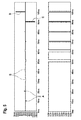
- FIG 5 a simulation is illustrated using the second embodiment of a crash detection circuit 200.
- two diagrams are shown in figure 5 .
- the upper diagram shows different crash pulses which are given as an input for the crash detection circuit 200 within the crash signal generation circuit 180.
- the lower diagram shows the evaluation of the crash detection circuit 200 at its output 79. It can be seen from figure 5 that the crash pulses denoted A have a duration which is too short to fulfill the fire condition (see figure 1 ), while the crash pulses denoted B have a current amplitude that is too low to fulfill the fire condition (see figure 1 ), as no output signal is generated and outputted at the output 79 of the crash detection circuit 200.
Abstract
Description
- The present invention relates to a crash detection circuit for the detection of a crash of a vehicle. The crash detection circuit comprises a transformer, a first comparator comprising an output and an inverting and a non-inverting input. Furthermore, the crash detection circuit comprises a window comparator.
- In crash detection circuits used for the detection of a crash of a vehicle, optocoupler units are often arranged in between a crash signal generation circuit and a crash signal evaluation circuit. The aforementioned optocoupler units serve to galvanically isolate the crash signal generation circuit of the vehicle from the electronics of the crash signal evaluation circuit of the same. However, such crash detection approaches which are based on optocoupler units often are expensive, lack a sufficient robustness, have a relatively short lifetime and do not allow for the transmittance of differentiated (positive and negative) signals, as the signaling between the crash signal generation circuit and the crash signal evaluation circuit is solely performed via light pulses.
- A crash detection circuit of the state of the art needs to fulfill a plurality of conditions. According to a first, so called no-fire condition, the crash detection circuit shall not detect a crash when a current in the crash signal generation circuit is smaller than or equal to 0.4A and when a current impulse given in the crash signal generation circuit is smaller than or equal to 5A and has a duration that is smaller than or equal to 4µs.
- According to a second, so called fire condition, the crash detection circuit shall detect a crash when a current in the crash signal generation circuit is greater than or equal to 1.75A and smaller than or equal to 40A for a duration of maximum 0.5ms in a predefined operating temperature range and when, for a duration that is smaller than or equal to 2ms, a current given in the crash signal generation circuit is greater than or equal to 1.2A and has a duration that is smaller than or equal to 4µs.
- In
figure 1 , the fire condition and the non-fire condition are illustrated in a coordinate system. The ordinate of the coordinate system shows the current given within the crash signal generation circuit and the abscissa shows the duration for which the respective current is given within the crash signal generation circuit. Infigure 1 , the dark plains illustrate an area in which the fire condition is fulfilled and the bright plains illustrate an area in which the non-fire condition is fulfilled. - One or more of the drawbacks of the prior art could be avoided or at least reduced by means of the present invention. In particular, it is provided a crash detection circuit for the detection of a crash of a vehicle. The crash detection circuit comprises a transformer, the transformer comprising a first inductor forming a part of a crash signal generation circuit and a second inductor forming a part of a crash signal evaluation circuit, the second inductor being galvanically isolated from the first inductor. Furthermore, the crash detection circuit comprises a first comparator comprising an output and an inverting and a non-inverting input, each input being electrically coupled to a terminal of the second inductor of the transformer respectively. Moreover, the crash detection circuit comprises a window comparator comprising a first input terminal for an input voltage to be evaluated and two second input terminals for reference voltages, wherein the output of the first comparator is electrically connected to the first input terminal of the window comparator.
- An advantage of such a crash detection circuit is that it is less expensive and has a higher robustness than alternative solutions of the state of the art, e.g. solutions using optocoupler units. Furthermore, such crash detection circuits have a longer lifetime, as more robust components come to use and are adapted to transmit positive and negative signals.
- Furthermore preferred, the window comparator further comprises an output for a crash signal evaluation signal.
- Preferably, the reference voltages inputted into the second input terminals define the size of the voltage window of the window comparator.
- Preferably, the crash detection circuit further comprises a voltage divider circuit comprising at least two resistors connected in series, wherein a terminal of one of the at least two resistors is electrically connected to the non-inverting input of the first comparator. The use of such a voltage divider circuit together with the first comparator and the window comparator allows for the fire condition and the non-fire condition to be implemented within the crash detection circuit. Expressed in other words, the use of such a voltage divider circuit together with the first comparator and the window comparator allows for the crash detection circuit to output a signal indicating the detection of a crash when the fire condition is met and to output a signal indicating that a crash was not detected when the non-fire condition is met. For this purpose, the values of the at least two resistors are chosen such that the crash detection circuit is adapted to continuously control whether the fire condition or the non-fire condition is met.
- Moreover preferred, another terminal of one of the at least two resistors is electrically connected to one of the two second input terminals of the window comparator and wherein another terminal of one of the at least two resistors is electrically connected to the other one of the two second input terminals of the window comparator. In such an embodiment, the voltage window of the window comparator is defined by constant reference voltages provided by the voltage divider circuit which allows for an efficient design of the crash detection circuit, as the resistors of the voltage divider circuit are used for a plurality of purposes.
- Preferably, the voltage divider circuit comprises four series connected resistors, wherein the non-inverting input of the first comparator is electrically connected to a terminal of one of the four resistors, wherein the aforementioned terminal electrically connects the second and the third resistor, counted from one of the outermost resistors of the four series connected resistors. In such an embodiment, the threshold voltages or reference voltages defining the voltage window of the window comparator can be chosen in a more precise manner, as more resistors allow for a division of the voltage supplied to the voltage divider circuit into smaller fractions. Preferably, all resistors of the voltage divider circuit have the same value, dividing the voltage supplied to the voltage divider circuit into equal fractions. In such an embodiment, a potential is supplied to the non-inverting input of the first comparator which is equal to half the voltage supplied to the voltage divider circuit. Preferably, the voltage divider circuit comprises four series connected resistors, wherein the non-inverting input of the first comparator is electrically connected to a terminal of one of the four resistors, wherein the aforementioned terminal electrically connects the first and the second resistor or the third and the fourth resistor, counted from one of the outermost resistors of the four series connected resistors.
- In a preferred embodiment, one of the two second input terminals of the window comparator is electrically connected to a terminal of the first resistor, wherein the aforementioned terminal electrically connects the first resistor with the second resistor. Preferably, the other one of the two second input terminals of the window comparator is electrically connected to a terminal of the third resistor, wherein the aforementioned terminal electrically connects the third resistor with the fourth resistor. In such an embodiment, the size of the voltage window of the window comparator is defined by the voltage which drops at the series connection of the second and third resistor. With such a realization, a crash detection circuit is provided that comprises a cost-efficient design allowing for a reduction of components that come to use when compared to alternative realizations known in the state of the art.
- In a preferred embodiment, the terminal of the first resistor which is not connected to the second resistor is electrically connected to a first voltage potential and wherein the terminal of the fourth resistor which is not connected to the third resistor is electrically connected to a second voltage potential, the first voltage potential being greater than the second voltage potential. Preferably, the terminal of the first resistor which is not connected to the second resistor is electrically connected to a first voltage potential which is equal to 5V. Furthermore preferred, the terminal of the fourth resistor which is not connected to the third resistor is electrically connected to a second voltage potential which is equal to the GND potential.
- Preferably, the second input terminal of the window comparator that is electrically connected to a terminal of the first resistor is an inverting input of the window comparator and wherein the second input terminal of the window comparator that is electrically connected to a terminal of the third resistor is a non-inverting input of the window comparator. In such a realization, the potential supplied to the inverting input of the window comparator denotes an upper boarder of the voltage window of the window comparator. Furthermore, the potential supplied to the non-inverting input of the window comparator denotes a lower boarder of the voltage window of the window comparator. In such an embodiment, the voltage at the output of the window comparator depends on the result of a comparison of the output voltage at the output of the first comparator with the voltages supplied to the second input terminals of the second inductor, thus to the upper and lower boarder of the voltage window of the window comparator. Expressed in other words, the window comparator compares the output voltage of the first comparator to the reference voltages inputted into the second input terminals of the window comparator. Preferably, the window comparator outputs a low signal, when the output voltage of the first comparator falls into the voltage window of the window comparator. Furthermore preferred, the window comparator outputs a high signal when the output voltage of the first comparator falls out of the voltage window of the window comparator.
- In a preferred embodiment, the first comparator is an operational amplifier. Operational amplifiers have a low voltage offset and are very precise amplifiers.
- Preferably, the crash detection circuit further comprises a parallel circuit of a resistor and a capacitor, wherein the output of the first comparator is electrically connected to a first terminal of the parallel circuit and wherein a second terminal of the parallel circuit is electrically connected to the inverting input of the first comparator. Such a parallel circuit in the feedback connection of the first comparator adapts and adjusts the time constant of the first comparator, allowing for the aforementioned implementation of the fire condition and the non-fire condition.
- Preferably, a resistor is connected in series to the first inductor. In such an embodiment, the resistance of the input clamps of the crash signal generation circuit is adapted.
- In a preferred embodiment, a further resistor is arranged within the electrical connection between the inverting input of the first comparator and the terminal of the second inductor. Also this resistor is used to precisely adjust the time constant of the first comparator.
- Preferably, the transformer is a current transformer. In such an embodiment, the crash detection circuit is advantageously usable with existing current generation sources present in vehicles, wherein such current generation sources are adapted to generate a current in case of a crash. The current generation source for example can be a current source that is the emulation of a crash signal according to a standard of a vehicle manufacturer.
- In an alternative, preferred embodiment, the transformer is a voltage transformer. In such an embodiment, the crash detection circuit is advantageously usable with existing voltage sources present in vehicles, wherein such voltage sources are adapted to generate a voltage in case of a crash. The voltage source for example can be a voltage source that is the emulation of a crash signal according to a standard of a vehicle manufacturer.
- Preferably, at least one resistor is connected in series and/or in parallel to the first inductor. Such an embodiment is especially suited when the transformer is a voltage transformer. In such an embodiment, the at least one resistor is used to limit the voltage supplied to the first inductor of the transformer.
- Moreover, a vehicle including a crash detection circuit according to the invention is provided. In such an embodiment, the crash detection of the vehicle is improved for the aforementioned reasons.
- Features will become apparent to those of ordinary skill in the art by describing in detail exemplary embodiments with reference to the attached drawings in which:
- Fig. 1
- shows a coordinate system with areas therein illustrating the fire condition and the non-fire condition;
- Fig. 2
- illustrates a first embodiment of a crash detection circuit;
- Fig. 3
- illustrates a second embodiment of a crash detection circuit with a current transformer;
- Fig. 4
- illustrates a third embodiment of a crash detection circuit with a voltage transformer, and
- Fig. 5
- illustrates a simulation using the second embodiment of a crash detection circuit.
- Reference will now be made in detail to embodiments, examples of which are illustrated in the accompanying drawings. Effects and features of the exemplary embodiments will be described with reference to the accompanying drawings. In the drawings, like reference numerals denote like elements, and redundant descriptions are omitted. As used herein, the term "and/or" includes any and all combinations of one or more of the associated listed items. Further, the use of "may" when describing embodiments of the present invention refers to "one or more embodiments of the present invention."
- It will be understood that although the terms "first" and "second" are used to describe various elements, these elements should not be limited by these terms. These terms are only used to distinguish one element from another element. For example, a first element may be named a second element and, similarly, a second element may be named a first element, without departing from the scope of the present invention.
- In the following description of embodiments of the present invention, the terms of a singular form may include plural forms unless the context clearly indicates otherwise.
- The present invention, may be embodied in various different forms, and should not be construed as being limited to only the illustrated embodiments herein. Rather, these embodiments are provided as examples so that this disclosure will be thorough and complete, and will fully convey the aspects and features of the present invention to those skilled in the art. Accordingly, elements and techniques that are not necessary to those having ordinary skill in the art for a complete understanding of the aspects and features of the present invention may not be described.
- It will be understood that, although the terms "first," "second," "third," etc., may be used herein to describe various elements and/or components, these elements and/or components should not be limited by these terms. These terms are used to distinguish one element and/or component from another element and/or component. Thus, a first element and/or component described below could be termed a second element and/or component, without departing from the scope of the present invention.
- It will be understood that when an element or component is referred to as being "on," "connected to," or "coupled to" another element or component, it can be directly on, connected to, or coupled to the other element or component, or one or more intervening elements or components may be present. In addition, it will also be understood that when an element or component is referred to as being "between" two elements or components, it can be the only element or component between the two elements or components, or one or more intervening elements or components may also be present.
- The terminology used herein is for the purpose of describing particular embodiments only and is not intended to be limiting of the present invention. As used herein, the singular forms "a," "an," and "the" are intended to include the plural forms as well, unless the context clearly indicates otherwise. It will be further understood that the terms "comprises," "comprising," "includes," and "including," when used in this specification, specify the presence of the stated features, integers, operations, elements, and/or components, but do not preclude the presence or addition of one or more other features, integers, operations, elements, components, and/or groups thereof. As used herein, the term "and/or" includes any and all combinations of one or more of the associated listed items. Expressions such as "at least one of," when preceding a list of elements, modify the entire list of elements and do not modify the individual elements of the list.
- As used herein, the term "substantially," "about," and similar terms are used as terms of approximation and not as terms of degree, and are intended to account for the inherent deviations in measured or calculated values that would be recognized by those of ordinary skill in the art. Further, if the term "substantially" is used in combination with a feature that could be expressed using a numeric value, the term "substantially" denotes a range of +/- 5% of the value centered on the value.
-
Figure 2 illustrates a first embodiment of acrash detection circuit 200. In this first embodiment, thecrash detection circuit 200 is implemented into a vehicle (not shown infigure 2 ) and adapted to detect a crash of this aforementioned vehicle. Thecrash detection circuit 200 substantially comprises two sub-circuits which are galvanically isolated from each other. The first sub-circuit is a crashsignal generation circuit 180 which is adapted to generate a crash signal. This crash signal can be represented by a current or a voltage which can be generated by a current source or a voltage source respectively. The second sub-circuit is a crashsignal evaluation circuit 170 which is adapted to evaluate the signal generated by the crashsignal generation circuit 180. - The
crash detection circuit 200 comprises atransformer 90 which comprises afirst inductor 91 forming a part of the crashsignal generation circuit 180 and asecond inductor 92 which forms a part of the crashsignal evaluation circuit 170. The first and thesecond inductor crash detection circuit 200 further comprises afirst comparator 80 which comprises anoutput 85, an invertinginput 81 and anon-inverting input 82, eachinput second inductor 92 of thetransformer 90 respectively. Expressed in other words, the invertinginput 81 of thefirst comparator 80 is electrically connected to a first terminal of thesecond inductor 92 and thenon-inverting input 82 is electrically connected to a second terminal of thesecond inductor 92. Furthermore, thecrash detection circuit 200 comprises awindow comparator 70. Thewindow comparator 70 comprises afirst input terminal 75 for an input voltage to be evaluated and twosecond input terminals window comparator 70 and are supplied to the twosecond input terminals second input terminals 71 and defines an upper boarder of the voltage window of thewindow comparator 70, wherein the second reference voltage Uref2 is supplied to the second of the twosecond input terminals 72 and defines a lower boarder of the voltage window of thewindow comparator 70. In this first embodiment, the reference voltages Urf1, Uref2 are constant and supplied by a further component of the crashsignal evaluation circuit 170 which infigure 2 is not shown. Moreover, in this first embodiment, the mean value Umean of the reference voltages Urf1, Uref1 is supplied to thenon-inverting input 82 of thefirst comparator 80, wherein the mean value Umean is equal to (Uref1 + Uref2)/2. In this first embodiment, the mean value Umean is supplied to thenon-inverting input 82 of thefirst comparator 80 via the aforementioned further component. However, it can also be provided to thenon-inverting input 82 via another component. - The
output 85 of thefirst comparator 80 is electrically connected to thefirst input terminal 75 of thewindow comparator 70. Thus, the signal outputted by theoutput 85 of thefirst comparator 80 is compared to the reference voltages Uref1, Uref2. In this first embodiment, the reference voltages are chosen such that the crashsignal evaluation circuit 170 continuously evaluates whether the fire condition or the non-fire condition as shown in the coordinate system offigure 1 are met. Thus, thewindow comparator 70 outputs a corresponding signal via itsoutput 79 when the fire condition is met and a crash has been successfully detected. - In
figure 3 , a second embodiment of acrash detection circuit 200 with acurrent transformer 90 is shown. Also in this second embodiment, thecrash detection circuit 200 comprises a crashsignal generation circuit 180 and a crashsignal evaluation circuit 170. The crashsignal generation circuit 180 comprises acurrent source 181 for the generation of a current corresponding to a crash signal. Infigure 3 , thecurrent source 181 is shown as a single component. However, the current within the crashsignal generation circuit 180 can be generated via a plurality of components which infigure 3 are not shown. Furthermore, thecrash detection circuit 200 comprises atransformer 90, which in this second embodiment is realized as acurrent transformer 90. Via thefirst inductor 91 of thecurrent transformer 90, a current can be induced in thesecond inductor 92 which forms a part of the crashsignal evaluation circuit 170. In this second embodiment, thefirst comparator 80 is realized as an operational amplifier, wherein the invertinginput 81 of the operational amplifier is electrically connected to a first terminal of thesecond inductor 92 and wherein thenon-inverting input 82 of the operational amplifier is electrically connected to a second terminal of thesecond inductor 92. A firstpower supply terminal 84 of the operational amplifier is electrically connected to a potential of 5V, wherein the otherpower supply terminal 86 of the operational amplifier is electrically connected to a GND potential. - In this second embodiment, the crash
signal evaluation circuit 170 further comprises avoltage divider circuit 160 that comprises four series connectedresistors voltage divider circuit 160 comprises afirst terminal 161 electrically connected to afirst resistor 61. Thisfirst resistor 61 is electrically connected to asecond resistor 62, which is electrically connected to athird resistor 63. Thisthird resistor 63 is electrically connected to afourth resistor 64 which is electrically connected to asecond terminal 162 of thevoltage divider circuit 160. In this second embodiment, the first, second, third andfourth resistor fourth resistor voltage divider circuit 160 can comprise three or more than four resistors. - Furthermore, in this second embodiment, the
first terminal 161 of thevoltage divider circuit 160 is electrically connected to a potential of exemplarily 5V, wherein thesecond terminal 162 of thevoltage divider circuit 160 is exemplarily electrically connected to the GND potential. However, the first andsecond terminal voltage divider circuit 160 can also be connected to other potentials. In this second embodiment, thenon-inverting input 82 of thefirst comparator 80 is electrically connected to a terminal of one of the fourresistors third resistor outermost resistors resistors non-inverting input 82 of thefirst comparator 80 is directly electrically connected to the terminals of the second andthird resistor - In this second embodiment, one of the two
second input terminals 71 of thewindow comparator 70 is electrically connected to a terminal of thefirst resistor 61, wherein the aforementioned terminal electrically connects thefirst resistor 61 with thesecond resistor 62. In more detail, in this second embodiment, the first of the twosecond input terminals 71 of thewindow comparator 70, which exemplarily is an inverting input terminal of thewindow comparator 70, is directly electrically connected to the terminals of the first andsecond resistor second input terminals 72 of thewindow comparator 70, which exemplarily is a non-inverting input terminal of thewindow comparator 70, is directly electrically connected to the terminal of thethird resistor 63 which is directly connected to thefourth resistor 64. In more detail, in this second embodiment, the second of the twosecond input terminals 72 of thewindow comparator 70, which exemplarily is a non-inverting input terminal of thewindow comparator 70, is directly electrically connected to the terminals of the third andfourth resistor - In this second embodiment, the voltage drop across the second and
third resistor window comparator 70 which in this second embodiment exemplarily has a span of 2.5V. - The
output 85 of thefirst comparator 80 is electrically connected to thefirst input terminal 75 of thewindow comparator 80. Thewindow comparator 70 comprises two further comparators 70-1, 70-2 which also can be operational amplifiers. However, also other and further comparators can come to use, the other/further comparators together forming awindow comparator 70. - The
crash detection circuit 200 further comprises aparallel circuit 50 of aresistor 51 and acapacitor 52, wherein theoutput 85 of thefirst comparator 80 is electrically connected to a first terminal of theparallel circuit 50 and wherein a second terminal of theparallel circuit 50 is electrically connected to the invertinginput 81 of thefirst comparator 80. Expressed in other words, theparallel circuit 50 is arranged within the feedback circuit of thefirst comparator 80. Moreover, afurther resistor 55 is arranged within the electrical connection between the invertinginput 81 of thefirst comparator 80 and the terminal of thesecond inductor 92. Via theparallel circuit 50 and thefurther resistor 55, the time constant of the operational amplifier is adjusted according to the non-fire condition and the fire condition as illustrated infigure 1 . - Via the
output 79 of thewindow comparator 70, the crashsignal evaluation circuit 170 outputs an output signal which is according to the evaluation. -
Figure 4 illustrates a third embodiment of acrash detection circuit 200 with avoltage transformer 90. Thecrash detection circuit 200 shown infigure 4 is substantially identical to thecrash detection circuit 200 as shown infigure 3 . However, as in this third embodiment, avoltage transformer 90 comes to use, the crashsignal generation circuit 180 needs to be adapted. Thus, in this third embodiment, tworesistors 58 are connected in series to thefirst inductor 91 of thevoltage transformer 90, wherein afurther resistor 59 is connected in parallel to thefirst inductor 91 of thevoltage transformer 90. - In
figure 5 , a simulation is illustrated using the second embodiment of acrash detection circuit 200. In more detail, two diagrams are shown infigure 5 . The upper diagram shows different crash pulses which are given as an input for thecrash detection circuit 200 within the crashsignal generation circuit 180. The lower diagram shows the evaluation of thecrash detection circuit 200 at itsoutput 79. It can be seen fromfigure 5 that the crash pulses denoted A have a duration which is too short to fulfill the fire condition (seefigure 1 ), while the crash pulses denoted B have a current amplitude that is too low to fulfill the fire condition (seefigure 1 ), as no output signal is generated and outputted at theoutput 79 of thecrash detection circuit 200. - However, this is not the case for the crash pulses C and D which fulfill the fire condition (see
figure 1 ), as pulses are outputted at theoutput 79 of thecrash detection circuit 200, the pulses being visible within the lower diagram.
Claims (15)
- A crash detection circuit (200) for the detection of a crash of a vehicle, comprising:a transformer (90), comprising a first inductor (91) forming a part of a crash signal generation circuit (180) and a second inductor (92) forming a part of a crash signal evaluation circuit (170), the second inductor (92) being galvanically isolated from the first inductor (91);a first comparator (80) comprising an output (85) and an inverting and a non-inverting input (81, 82), each input (81, 82) being electrically coupled to a terminal of the second inductor (92) of the transformer (90) respectively, anda window comparator (70) comprising a first input terminal (75) for an input voltage to be evaluated and two second input terminals (71, 72) for reference voltages, wherein the output of the first comparator (80) is electrically connected to the first input terminal (75) of the window comparator (70).
- The crash detection circuit (200) of claim 1, further comprising a voltage divider circuit (160) comprising at least two resistors (61, 62) connected in series, wherein a terminal of one of the at least two resistors (61, 62) is electrically connected to the non-inverting input (82) of the first comparator (80).
- The crash detection circuit (200) of claim 2, wherein another terminal of one of the at least two resistors (61, 62) is electrically connected to one of the two second input terminals (71, 72) of the window comparator (70) and wherein another terminal of one of the at least two resistors (61, 62) is electrically connected to the other one of the two second input terminals (71, 72) of the window comparator (70).
- The crash detection circuit (200) of claim 2 or 3, wherein the voltage divider circuit (160) comprises four series connected resistors (61, 62, 63, 64), wherein the non-inverting input (82) of the first comparator (80) is electrically connected to a terminal of one of the four resistors (62, 63), wherein the aforementioned terminal electrically connects the second and the third resistor (62, 63), counted from one of the outermost resistors (61, 64) of the four series connected resistors (61, 62, 63, 64).
- The crash detection circuit (200) of claim 4, wherein one of the two second input terminals (71) of the window comparator (70) is electrically connected to a terminal of the first resistor (61), wherein the aforementioned terminal electrically connects the first resistor (61) with the second resistor (62).
- The crash detection circuit (200) of claim 5, wherein the other one of the two second input terminals (72) of the window comparator (70) is electrically connected to a terminal of the third resistor (63), wherein the aforementioned terminal electrically connects the third resistor (63) with the fourth resistor (64).
- The crash detection circuit (200) of one of the claims 4 to 6, wherein the terminal of the first resistor (61) which is not connected to the second resistor (62) is electrically connected to a first voltage potential and wherein the terminal of the fourth resistor (64) which is not connected to the third resistor (63) is electrically connected to a second voltage potential, the first voltage potential being greater than the second voltage potential.
- The crash detection circuit (200) of claim 6 and 7, wherein the second input terminal (71) of the window comparator (70) that is electrically connected to a terminal of the first resistor (61) is an inverting input of the window comparator (70) and wherein the second input terminal (72) of the window comparator (70) that is electrically connected to a terminal of the third resistor (63) is a non-inverting input of the window comparator (70).
- The crash detection circuit (200) of any one of the preceding claims, wherein the first comparator (80) is an operational amplifier.
- The crash detection circuit (200) of any one of the preceding claims, further comprising a parallel circuit (50) of a resistor (51) and a capacitor (52), wherein the output (85) of the first comparator (80) is electrically connected to a first terminal of the parallel circuit (50) and wherein a second terminal of the parallel circuit (50) is electrically connected to the inverting input (81) of the first comparator (80).
- The crash detection circuit (200) of any one of the preceding claims, wherein a further resistor (55) is arranged within the electrical connection between the inverting input (81) of the first comparator (80) and the terminal of the second inductor (92).
- The crash detection circuit (200) of any one of the preceding claims, wherein the transformer (90) is a current transformer.
- The crash detection circuit (200) of one of the claims 1 to 11, wherein the transformer (90) is a voltage transformer.
- The crash detection circuit (200) of claim 13, wherein at least one resistor (58) is connected in series and/or in parallel to the first inductor (91).
- A vehicle including a crash detection circuit (200) according to any one of the preceding claims.
Priority Applications (2)
| Application Number | Priority Date | Filing Date | Title |
|---|---|---|---|
| EP16195835.0A EP3315918B1 (en) | 2016-10-26 | 2016-10-26 | Crash detection circuit for the detection of a crash of a vehicle |
| US15/420,914 US10414350B2 (en) | 2016-10-26 | 2017-01-31 | Crash detection circuit for the detection of a crash of a vehicle |
Applications Claiming Priority (1)
| Application Number | Priority Date | Filing Date | Title |
|---|---|---|---|
| EP16195835.0A EP3315918B1 (en) | 2016-10-26 | 2016-10-26 | Crash detection circuit for the detection of a crash of a vehicle |
Publications (2)
| Publication Number | Publication Date |
|---|---|
| EP3315918A1 true EP3315918A1 (en) | 2018-05-02 |
| EP3315918B1 EP3315918B1 (en) | 2018-08-22 |
Family
ID=57354096
Family Applications (1)
| Application Number | Title | Priority Date | Filing Date |
|---|---|---|---|
| EP16195835.0A Active EP3315918B1 (en) | 2016-10-26 | 2016-10-26 | Crash detection circuit for the detection of a crash of a vehicle |
Country Status (2)
| Country | Link |
|---|---|
| US (1) | US10414350B2 (en) |
| EP (1) | EP3315918B1 (en) |
Citations (4)
| Publication number | Priority date | Publication date | Assignee | Title |
|---|---|---|---|---|
| EP0723161A1 (en) * | 1994-08-08 | 1996-07-24 | The Nippon Signal Co. Ltd. | Trouble monitor device for bridge circuit |
| US5568131A (en) * | 1993-03-31 | 1996-10-22 | The Nippon Signal Co., Ltd. | Motor rotation judgement circuit and apparatus using such circuit for verifying that a motor is stopped |
| US5717302A (en) * | 1994-09-30 | 1998-02-10 | The Nippon Signal Co., Ltd. | Motor stopped verification apparatus |
| US20140327992A1 (en) * | 2008-08-15 | 2014-11-06 | David L Sykes | Arc suppression circuit |
Family Cites Families (10)
| Publication number | Priority date | Publication date | Assignee | Title |
|---|---|---|---|---|
| JPH0753499B2 (en) | 1988-05-12 | 1995-06-07 | 三菱電機株式会社 | Failure detection device for airbag device |
| US6015484A (en) * | 1997-11-26 | 2000-01-18 | Gamry Instruments, Inc. | Detection of pitting corrosion |
| JP3578959B2 (en) * | 2000-02-24 | 2004-10-20 | 松下電器産業株式会社 | Table tap and monitoring system using the table tap |
| GB0015349D0 (en) * | 2000-06-23 | 2000-08-16 | Atherton Eric | Corrosion monitoring |
| CA2561935A1 (en) * | 2004-04-09 | 2005-10-27 | Southwest Research Institute | Improved method for measuring localized corrosion rate with a multi-electrode array sensor |
| US20110075158A1 (en) * | 2009-09-30 | 2011-03-31 | Delphi Technologies, Inc. | Optical crash sensor |
| US20120098518A1 (en) * | 2010-04-23 | 2012-04-26 | Panasonic Corporation | Detection apparatus and detection system |
| EP2574948B1 (en) * | 2011-09-09 | 2017-08-30 | GS Yuasa International Ltd. | Electric storage device monitor |
| JP2013238472A (en) | 2012-05-15 | 2013-11-28 | Renesas Electronics Corp | Semiconductor device and voltage measurement device |
| KR20150118730A (en) | 2014-04-15 | 2015-10-23 | 엘에스산전 주식회사 | Fault detection circuit of inverter |
-
2016
- 2016-10-26 EP EP16195835.0A patent/EP3315918B1/en active Active
-
2017
- 2017-01-31 US US15/420,914 patent/US10414350B2/en active Active
Patent Citations (4)
| Publication number | Priority date | Publication date | Assignee | Title |
|---|---|---|---|---|
| US5568131A (en) * | 1993-03-31 | 1996-10-22 | The Nippon Signal Co., Ltd. | Motor rotation judgement circuit and apparatus using such circuit for verifying that a motor is stopped |
| EP0723161A1 (en) * | 1994-08-08 | 1996-07-24 | The Nippon Signal Co. Ltd. | Trouble monitor device for bridge circuit |
| US5717302A (en) * | 1994-09-30 | 1998-02-10 | The Nippon Signal Co., Ltd. | Motor stopped verification apparatus |
| US20140327992A1 (en) * | 2008-08-15 | 2014-11-06 | David L Sykes | Arc suppression circuit |
Also Published As
| Publication number | Publication date |
|---|---|
| EP3315918B1 (en) | 2018-08-22 |
| US20180111572A1 (en) | 2018-04-26 |
| US10414350B2 (en) | 2019-09-17 |
Similar Documents
| Publication | Publication Date | Title |
|---|---|---|
| EP3468303B1 (en) | A led lamp having an outage detection circuit | |
| US8031452B2 (en) | Single-supply single-ended high voltage peak detector | |
| US9307612B2 (en) | Light emitting device driver circuit and driving method of light emitting device circuit | |
| JP2009200944A (en) | Hysteresis comparator | |
| US20150355289A1 (en) | Electronic device | |
| US10317248B2 (en) | Multiple-distance proximity sensor systems | |
| EP3315918B1 (en) | Crash detection circuit for the detection of a crash of a vehicle | |
| US8519744B2 (en) | Method of utilizing dual comparators to facilitate a precision signal rectification and timing system without signal feedback | |
| US10361570B2 (en) | Charging/discharging control circuit and battery apparatus including voltage or current detection for secondary batteries | |
| JP6461561B2 (en) | Igniters and vehicles | |
| JP2006349466A (en) | Temperature detecting device | |
| TWI512310B (en) | Three-phase source detection device | |
| TWI722766B (en) | Frequency detection circuit | |
| JP5950084B2 (en) | Condition monitoring device | |
| JP7103085B2 (en) | State detector | |
| US20190235006A1 (en) | Wiring line abnormality detecting device | |
| KR101603251B1 (en) | Converter for led light in constant current type and led light apparatus using it | |
| CN105698333B (en) | position sensing device of infrared source, control device of fan blade and temperature adjusting equipment | |
| KR20150145683A (en) | Data signal receiving circuit for controling lighting | |
| US7589505B2 (en) | Power supply with reliable voltage feedback control independent of any ground voltage difference | |
| CN110389306B (en) | Detection device and detection method | |
| JP2014062825A (en) | Voltage detection circuit, and voltage detection method | |
| KR101409086B1 (en) | Judging Circuit For State Of Static Voltage | |
| JP5900090B2 (en) | Bottom detection circuit | |
| JPH05291899A (en) | Hysteresis comparator circuit |
Legal Events
| Date | Code | Title | Description |
|---|---|---|---|
| PUAI | Public reference made under article 153(3) epc to a published international application that has entered the european phase |
Free format text: ORIGINAL CODE: 0009012 |
|
| 17P | Request for examination filed |
Effective date: 20170919 |
|
| AK | Designated contracting states |
Kind code of ref document: A1 Designated state(s): AL AT BE BG CH CY CZ DE DK EE ES FI FR GB GR HR HU IE IS IT LI LT LU LV MC MK MT NL NO PL PT RO RS SE SI SK SM TR |
|
| AX | Request for extension of the european patent |
Extension state: BA ME |
|
| GRAP | Despatch of communication of intention to grant a patent |
Free format text: ORIGINAL CODE: EPIDOSNIGR1 |
|
| INTG | Intention to grant announced |
Effective date: 20180530 |
|
| GRAS | Grant fee paid |
Free format text: ORIGINAL CODE: EPIDOSNIGR3 |
|
| GRAA | (expected) grant |
Free format text: ORIGINAL CODE: 0009210 |
|
| AK | Designated contracting states |
Kind code of ref document: B1 Designated state(s): AL AT BE BG CH CY CZ DE DK EE ES FI FR GB GR HR HU IE IS IT LI LT LU LV MC MK MT NL NO PL PT RO RS SE SI SK SM TR |
|
| REG | Reference to a national code |
Ref country code: GB Ref legal event code: FG4D |
|
| REG | Reference to a national code |
Ref country code: CH Ref legal event code: EP |
|
| REG | Reference to a national code |
Ref country code: AT Ref legal event code: REF Ref document number: 1033032 Country of ref document: AT Kind code of ref document: T Effective date: 20180915 |
|
| REG | Reference to a national code |
Ref country code: IE Ref legal event code: FG4D |
|
| REG | Reference to a national code |
Ref country code: DE Ref legal event code: R096 Ref document number: 602016004969 Country of ref document: DE |
|
| REG | Reference to a national code |
Ref country code: FR Ref legal event code: PLFP Year of fee payment: 3 |
|
| REG | Reference to a national code |
Ref country code: NL Ref legal event code: MP Effective date: 20180822 |
|
| REG | Reference to a national code |
Ref country code: LT Ref legal event code: MG4D |
|
| PG25 | Lapsed in a contracting state [announced via postgrant information from national office to epo] |
Ref country code: LT Free format text: LAPSE BECAUSE OF FAILURE TO SUBMIT A TRANSLATION OF THE DESCRIPTION OR TO PAY THE FEE WITHIN THE PRESCRIBED TIME-LIMIT Effective date: 20180822 Ref country code: FI Free format text: LAPSE BECAUSE OF FAILURE TO SUBMIT A TRANSLATION OF THE DESCRIPTION OR TO PAY THE FEE WITHIN THE PRESCRIBED TIME-LIMIT Effective date: 20180822 Ref country code: NL Free format text: LAPSE BECAUSE OF FAILURE TO SUBMIT A TRANSLATION OF THE DESCRIPTION OR TO PAY THE FEE WITHIN THE PRESCRIBED TIME-LIMIT Effective date: 20180822 Ref country code: BG Free format text: LAPSE BECAUSE OF FAILURE TO SUBMIT A TRANSLATION OF THE DESCRIPTION OR TO PAY THE FEE WITHIN THE PRESCRIBED TIME-LIMIT Effective date: 20181122 Ref country code: SE Free format text: LAPSE BECAUSE OF FAILURE TO SUBMIT A TRANSLATION OF THE DESCRIPTION OR TO PAY THE FEE WITHIN THE PRESCRIBED TIME-LIMIT Effective date: 20180822 Ref country code: RS Free format text: LAPSE BECAUSE OF FAILURE TO SUBMIT A TRANSLATION OF THE DESCRIPTION OR TO PAY THE FEE WITHIN THE PRESCRIBED TIME-LIMIT Effective date: 20180822 Ref country code: IS Free format text: LAPSE BECAUSE OF FAILURE TO SUBMIT A TRANSLATION OF THE DESCRIPTION OR TO PAY THE FEE WITHIN THE PRESCRIBED TIME-LIMIT Effective date: 20181222 Ref country code: GR Free format text: LAPSE BECAUSE OF FAILURE TO SUBMIT A TRANSLATION OF THE DESCRIPTION OR TO PAY THE FEE WITHIN THE PRESCRIBED TIME-LIMIT Effective date: 20181123 Ref country code: NO Free format text: LAPSE BECAUSE OF FAILURE TO SUBMIT A TRANSLATION OF THE DESCRIPTION OR TO PAY THE FEE WITHIN THE PRESCRIBED TIME-LIMIT Effective date: 20181122 |
|
| PG25 | Lapsed in a contracting state [announced via postgrant information from national office to epo] |
Ref country code: HR Free format text: LAPSE BECAUSE OF FAILURE TO SUBMIT A TRANSLATION OF THE DESCRIPTION OR TO PAY THE FEE WITHIN THE PRESCRIBED TIME-LIMIT Effective date: 20180822 Ref country code: LV Free format text: LAPSE BECAUSE OF FAILURE TO SUBMIT A TRANSLATION OF THE DESCRIPTION OR TO PAY THE FEE WITHIN THE PRESCRIBED TIME-LIMIT Effective date: 20180822 Ref country code: AL Free format text: LAPSE BECAUSE OF FAILURE TO SUBMIT A TRANSLATION OF THE DESCRIPTION OR TO PAY THE FEE WITHIN THE PRESCRIBED TIME-LIMIT Effective date: 20180822 |
|
| PG25 | Lapsed in a contracting state [announced via postgrant information from national office to epo] |
Ref country code: RO Free format text: LAPSE BECAUSE OF FAILURE TO SUBMIT A TRANSLATION OF THE DESCRIPTION OR TO PAY THE FEE WITHIN THE PRESCRIBED TIME-LIMIT Effective date: 20180822 Ref country code: CZ Free format text: LAPSE BECAUSE OF FAILURE TO SUBMIT A TRANSLATION OF THE DESCRIPTION OR TO PAY THE FEE WITHIN THE PRESCRIBED TIME-LIMIT Effective date: 20180822 Ref country code: IT Free format text: LAPSE BECAUSE OF FAILURE TO SUBMIT A TRANSLATION OF THE DESCRIPTION OR TO PAY THE FEE WITHIN THE PRESCRIBED TIME-LIMIT Effective date: 20180822 Ref country code: EE Free format text: LAPSE BECAUSE OF FAILURE TO SUBMIT A TRANSLATION OF THE DESCRIPTION OR TO PAY THE FEE WITHIN THE PRESCRIBED TIME-LIMIT Effective date: 20180822 Ref country code: ES Free format text: LAPSE BECAUSE OF FAILURE TO SUBMIT A TRANSLATION OF THE DESCRIPTION OR TO PAY THE FEE WITHIN THE PRESCRIBED TIME-LIMIT Effective date: 20180822 Ref country code: PL Free format text: LAPSE BECAUSE OF FAILURE TO SUBMIT A TRANSLATION OF THE DESCRIPTION OR TO PAY THE FEE WITHIN THE PRESCRIBED TIME-LIMIT Effective date: 20180822 |
|
| REG | Reference to a national code |
Ref country code: DE Ref legal event code: R097 Ref document number: 602016004969 Country of ref document: DE |
|
| PG25 | Lapsed in a contracting state [announced via postgrant information from national office to epo] |
Ref country code: SK Free format text: LAPSE BECAUSE OF FAILURE TO SUBMIT A TRANSLATION OF THE DESCRIPTION OR TO PAY THE FEE WITHIN THE PRESCRIBED TIME-LIMIT Effective date: 20180822 Ref country code: DK Free format text: LAPSE BECAUSE OF FAILURE TO SUBMIT A TRANSLATION OF THE DESCRIPTION OR TO PAY THE FEE WITHIN THE PRESCRIBED TIME-LIMIT Effective date: 20180822 Ref country code: SM Free format text: LAPSE BECAUSE OF FAILURE TO SUBMIT A TRANSLATION OF THE DESCRIPTION OR TO PAY THE FEE WITHIN THE PRESCRIBED TIME-LIMIT Effective date: 20180822 |
|
| REG | Reference to a national code |
Ref country code: BE Ref legal event code: MM Effective date: 20181031 |
|
| PG25 | Lapsed in a contracting state [announced via postgrant information from national office to epo] |
Ref country code: MC Free format text: LAPSE BECAUSE OF FAILURE TO SUBMIT A TRANSLATION OF THE DESCRIPTION OR TO PAY THE FEE WITHIN THE PRESCRIBED TIME-LIMIT Effective date: 20180822 Ref country code: LU Free format text: LAPSE BECAUSE OF NON-PAYMENT OF DUE FEES Effective date: 20181026 |
|
| PLBE | No opposition filed within time limit |
Free format text: ORIGINAL CODE: 0009261 |
|
| STAA | Information on the status of an ep patent application or granted ep patent |
Free format text: STATUS: NO OPPOSITION FILED WITHIN TIME LIMIT |
|
| REG | Reference to a national code |
Ref country code: IE Ref legal event code: MM4A |
|
| 26N | No opposition filed |
Effective date: 20190523 |
|
| PG25 | Lapsed in a contracting state [announced via postgrant information from national office to epo] |
Ref country code: BE Free format text: LAPSE BECAUSE OF NON-PAYMENT OF DUE FEES Effective date: 20181031 Ref country code: SI Free format text: LAPSE BECAUSE OF FAILURE TO SUBMIT A TRANSLATION OF THE DESCRIPTION OR TO PAY THE FEE WITHIN THE PRESCRIBED TIME-LIMIT Effective date: 20180822 |
|
| PG25 | Lapsed in a contracting state [announced via postgrant information from national office to epo] |
Ref country code: IE Free format text: LAPSE BECAUSE OF NON-PAYMENT OF DUE FEES Effective date: 20181026 |
|
| PG25 | Lapsed in a contracting state [announced via postgrant information from national office to epo] |
Ref country code: MT Free format text: LAPSE BECAUSE OF NON-PAYMENT OF DUE FEES Effective date: 20181026 |
|
| PG25 | Lapsed in a contracting state [announced via postgrant information from national office to epo] |
Ref country code: TR Free format text: LAPSE BECAUSE OF FAILURE TO SUBMIT A TRANSLATION OF THE DESCRIPTION OR TO PAY THE FEE WITHIN THE PRESCRIBED TIME-LIMIT Effective date: 20180822 |
|
| PG25 | Lapsed in a contracting state [announced via postgrant information from national office to epo] |
Ref country code: PT Free format text: LAPSE BECAUSE OF FAILURE TO SUBMIT A TRANSLATION OF THE DESCRIPTION OR TO PAY THE FEE WITHIN THE PRESCRIBED TIME-LIMIT Effective date: 20180822 |
|
| REG | Reference to a national code |
Ref country code: CH Ref legal event code: PL |
|
| PG25 | Lapsed in a contracting state [announced via postgrant information from national office to epo] |
Ref country code: MK Free format text: LAPSE BECAUSE OF NON-PAYMENT OF DUE FEES Effective date: 20180822 Ref country code: HU Free format text: LAPSE BECAUSE OF FAILURE TO SUBMIT A TRANSLATION OF THE DESCRIPTION OR TO PAY THE FEE WITHIN THE PRESCRIBED TIME-LIMIT; INVALID AB INITIO Effective date: 20161026 Ref country code: CY Free format text: LAPSE BECAUSE OF FAILURE TO SUBMIT A TRANSLATION OF THE DESCRIPTION OR TO PAY THE FEE WITHIN THE PRESCRIBED TIME-LIMIT Effective date: 20180822 |
|
| PG25 | Lapsed in a contracting state [announced via postgrant information from national office to epo] |
Ref country code: LI Free format text: LAPSE BECAUSE OF NON-PAYMENT OF DUE FEES Effective date: 20191031 Ref country code: CH Free format text: LAPSE BECAUSE OF NON-PAYMENT OF DUE FEES Effective date: 20191031 |
|
| REG | Reference to a national code |
Ref country code: AT Ref legal event code: UEP Ref document number: 1033032 Country of ref document: AT Kind code of ref document: T Effective date: 20180822 |
|
| P01 | Opt-out of the competence of the unified patent court (upc) registered |
Effective date: 20230528 |
|
| PGFP | Annual fee paid to national office [announced via postgrant information from national office to epo] |
Ref country code: FR Payment date: 20230929 Year of fee payment: 8 |
|
| PGFP | Annual fee paid to national office [announced via postgrant information from national office to epo] |
Ref country code: GB Payment date: 20231006 Year of fee payment: 8 |
|
| PGFP | Annual fee paid to national office [announced via postgrant information from national office to epo] |
Ref country code: DE Payment date: 20230929 Year of fee payment: 8 Ref country code: AT Payment date: 20231009 Year of fee payment: 8 |