EP3314527B1 - Double-sided fingerprint sensor - Google Patents
Double-sided fingerprint sensor Download PDFInfo
- Publication number
- EP3314527B1 EP3314527B1 EP16751340.7A EP16751340A EP3314527B1 EP 3314527 B1 EP3314527 B1 EP 3314527B1 EP 16751340 A EP16751340 A EP 16751340A EP 3314527 B1 EP3314527 B1 EP 3314527B1
- Authority
- EP
- European Patent Office
- Prior art keywords
- drive
- pickup
- elements
- lines
- electrode pair
- Prior art date
- Legal status (The legal status is an assumption and is not a legal conclusion. Google has not performed a legal analysis and makes no representation as to the accuracy of the status listed.)
- Active
Links
Images


Classifications
-
- G—PHYSICS
- G06—COMPUTING OR CALCULATING; COUNTING
- G06V—IMAGE OR VIDEO RECOGNITION OR UNDERSTANDING
- G06V40/00—Recognition of biometric, human-related or animal-related patterns in image or video data
- G06V40/10—Human or animal bodies, e.g. vehicle occupants or pedestrians; Body parts, e.g. hands
- G06V40/12—Fingerprints or palmprints
- G06V40/13—Sensors therefor
- G06V40/1306—Sensors therefor non-optical, e.g. ultrasonic or capacitive sensing
-
- G—PHYSICS
- G06—COMPUTING OR CALCULATING; COUNTING
- G06V—IMAGE OR VIDEO RECOGNITION OR UNDERSTANDING
- G06V40/00—Recognition of biometric, human-related or animal-related patterns in image or video data
- G06V40/10—Human or animal bodies, e.g. vehicle occupants or pedestrians; Body parts, e.g. hands
- G06V40/12—Fingerprints or palmprints
- G06V40/1347—Preprocessing; Feature extraction
- G06V40/1359—Extracting features related to ridge properties; Determining the fingerprint type, e.g. whorl or loop
-
- G—PHYSICS
- G06—COMPUTING OR CALCULATING; COUNTING
- G06V—IMAGE OR VIDEO RECOGNITION OR UNDERSTANDING
- G06V40/00—Recognition of biometric, human-related or animal-related patterns in image or video data
- G06V40/10—Human or animal bodies, e.g. vehicle occupants or pedestrians; Body parts, e.g. hands
- G06V40/12—Fingerprints or palmprints
- G06V40/1382—Detecting the live character of the finger, i.e. distinguishing from a fake or cadaver finger
- G06V40/1394—Detecting the live character of the finger, i.e. distinguishing from a fake or cadaver finger using acquisition arrangements
Definitions
- This disclosure relates to sensors for the electronic sensing of objects located near or about the sensor, such as epidermal ridge patterns commonly known as fingerprints.
- Fingerprint sensors comprising electrodes for measuring characteristics in a finger surface are well known.
- US 7,110,577 , US 5,963,679 , US 6,069,970 , US 8,866,347 and 14/582,359 describe sensors based on different impedance or capacitance measurement principles with strip-shaped or matrix sensors comprising a number of individual sensor elements.
- Benkley US2012134549 ) describes a fingerprint sensor having a plurality of parallel pickup lines, a plurality of parallel drive lines oriented transverse to the pickup lines and a dielectric substrate layer separating the drive lines from the pickup lines.
- Jaechang's "A Double-sided Fingerprint Sensing Method” is directed to a fingerprint sensing method utilizing a double-sided fingerprint sensor configured to be held between a thumb and an index finger of a user.
- Fingerprint sensors are found in all kind of devices such as PC's, tablets, smart phones and smart cards for the security and ease of use it provides.
- the widespread use of fingerprint sensors may also provide a security problem as fingerprint sensors have been spoofed by spoof fingerprints produced from latent fingerprints.
- Current art fingerprint sensors typically attempt to mitigate this problem with additional security measures, such as live finger detection, at the cost of increased false rejection of fingerprints and reduced ease of use.
- a sensor comprising a plurality of substantially parallel upper pickup lines; a plurality of substantially parallel lower pickup lines; a plurality of substantially parallel drive lines oriented transversely to, and disposed between, the pluralities of upper and lower pickup lines; a first insulating layer separating the plurality of upper pickup lines from the plurality of drive lines; a second insulating layer opposite the first insulating layer, and separating the plurality of lower pickup lines from the plurality of drive lines; a plurality of upper electrode pairs, each upper electrode pair being defined at a location where an upper pickup line crosses a drive line, wherein each upper electrode pair has an impedance that is sensitive to a first object contacting or in close proximity to the upper electrode pair; and a plurality of lower electrode pairs, each lower electrode pair being defined at a location where a lower pickup line crosses a drive line, wherein each lower electrode pair has an impedance that is sensitive to a second object contacting or in close proximity to the lower electrode pair; wherein the plurality of substantially parallel drive lines comprises
- a two-sided fingerprint sensor assembly comprising:a first sensor side comprising upper pickup elements; a second sensor side in opposed relationship to the first sensor side and comprising lower pickup elements;drive elements disposed between the upper pickup elements and the lower pickup elements; a first insulating layer disposed between the drive elements and the upper pickup elements; a second insulating layer disposed between the drive elements and the lower pickup elements; a signal source configured to provide a drive signal to at least one of the drive elements that is configured to transmit the drive signal to the upper and lower pickup elements; and a detection system configured to sense the signal transmitted by the drive element to the upper and lower pickup elements and configured to detect features of a first fingerprint located proximately to the first sensor side based on a change in signal being received at the upper pickup elements and to detect features of a second fingerprint located proximately to the second sensor side based on changes in signal being received at the lower pickup elements; wherein the drive elements comprise:(a) a layer of upper drive elements, a layer of lower drive elements,
- the upper pickup lines and the lower pickup lines are oriented substantially perpendicular to the drive lines.
- the third insulating layer is made of glass, fiberglass, polycarbonate glass, polymer, a semiconductor material or a layered composite material.
- This description may use relative spatial and/or orientation terms in describing the position and/or orientation of a component, apparatus, location, feature, or a portion thereof. Unless specifically stated, or otherwise dictated by the context of the description, such terms, including, without limitation, top, bottom, above, below, under, on top of, upper, lower, left of, right of, in front of, behind, next to, adjacent, between, horizontal, vertical, diagonal, longitudinal, transverse, radial, axial, etc., are used for convenience in referring to such component, apparatus, location, feature, or a portion thereof in the drawings and are not intended to be limiting.
- any specific dimensions mentioned in this description are merely representative of an exemplary implementation of a device embodying aspects of the disclosure and are not intended to be limiting.
- the present disclosure relates to an electronic sensor for detecting proximally located objects.
- the sensor is a fingerprint sensor that detects surface features (e.g., ridges and valleys) of two fingers placed on the electronic sensor.
- the electronic sensor operates based on interaction between a pair of electrodes that include a drive element and a pickup element.
- the pickup element may be capacitively coupled to the drive element and may sense a signal that passes from the drive element to the pickup element.
- Features of a proximally located object can be detected based on whether the sensor detects a change in a signal being received at the pickup element.
- the electronic sensor includes a top, or upper, conductive grid and a bottom, or lower, conductive grid configured to detect surface features of two proximally located objects at a plurality of locations on two sides of the sensor.
- the top and bottom grids each include a plurality of parallel drive lines, which are each connectable to a drive source, and a plurality of parallel pickup lines that are oriented transversely (e.g., perpendicularly) to the drive lines.
- the drive lines are separated from the pickup lines by an insulating (e.g., dielectric) layer. Each drive line may thus be capacitively coupled to a pickup line.
- the drive lines can form one axis (e.g., X-axis) of the grid, while the pickup lines form another axis (e.g., Y-axis) of the grid.
- Each location where a drive line and a pickup line cross may form an impedance-sensitive electrode pair.
- This impedance-sensitive electrode pair may be treated as a pixel (e.g., an X-Y coordinate) at which a surface feature of the proximally located object is detected.
- the top and bottom grids form a plurality of pixels that can collectively be scanned to create a map of the surface features of the proximally located object.
- the pixels of the grid can differentiate locations where there is a ridge of a fingertip touching the electronic sensor and locations where there is a valley of the fingerprint.
- the map can be used as a pattern to match with ridge/valley patterns stored in a database.
- the grid sensor may create maps of two different fingers at the same time, typically a thumb and an index finger pinching the grid sensor. This makes it very difficult to find, develop, and align individual latent prints at the correct angles in order to spoof the sensor.
- the biomechanical angle of index print to thumb print may also be used as a secondary biometric.
- a prior art version of a fingerprint sensor with overlapping drive lines and pickup lines is discussed in more detail in U.S. Patent No. 8,421,890 , entitled “Electronic imager using an impedance sensor grid array and method of making” and U.S. application no 14/582,359 , entitled “Fingerprint sensor employing an integrated noise rejection structure.”
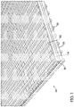
- FIG. 1 illustrates a portion of an exemplary sensor structure 100.
- the sensor 100 includes a middle conductive layer comprising a plurality of drive elements 101, an upper conductive layer comprising a plurality of upper pickup elements 102, and a lower conductive layer comprising a plurality of lower pickup elements 103.
- the drive elements 101 may be formed or etched as elongated, flat strips (i.e., width greater than thickness) of conductive material (e.g., copper, aluminum, gold) that are substantially parallel to each other and which may also be referred to as drive lines or drive plates.
- conductive material e.g., copper, aluminum, gold
- the upper and lower pickup elements 102, 103 may be formed or etched as elongated, flat strips of conductive material (e.g., copper, aluminum, gold) that are substantially parallel to each other and which may also be referred to as pickup lines or pickup plates.
- the upper pickup elements 102 may be aligned with the lower pickup elements 103.
- a first insulating layer 104 made of a dielectric material separates the drive lines 101 and the upper pickup lines 102.
- the drive elements 101 and the upper pickup elements 102 are oriented transversely to each other, and in one embodiment, are substantially perpendicular to each other, thereby forming an area of overlap between the drive lines 101 and the crossing upper pickup lines 102.
- a second insulating layer 105 made of a dielectric material separates the drive lines 101 and the lower pickup lines 103.
- the drive elements 101 and the lower pickup elements 103 are oriented transversely to each other, and in one embodiment, are substantially perpendicular to each other, thereby forming an area of overlap between the drive lines 101 and the lower crossing pickup lines 103.
- Each location where a drive element 101 and a pickup element 102, 103 cross forms an impedance-sensitive electrode pair - drive elements 101 and upper pickup elements 102 forming upper electrode pairs and drive elements 101 and lower pickup elements 103 forming lower electrode pairs.
- the impedance-sensitive electrode pair has a first impedance determined by the size of the parallel plate capacitor formed by the electrode pair, which is a function of the dimensions of the drive element 101 and dimensions of the pickup elements 102, 103 and the thickness and dielectric properties of the insulating layers 104, 105.
- the widths of the drive elements 101 and the pickup elements 102, 103 are equal, and thus the area of overlap defined by the width of the drive line and the width of the pickup line has equal width and length.
- Other configurations are possible in which the width of the drive elements 101 and the pickup elements 102, 103 are different.
- the width of each of the drive elements 101 is greater than (e.g., twice) the width of each of the pickup elements 102, 103, or vice versa.
- FIG. 2 illustrates a portion of an exemplary sensor structure 200 according to an alternate embodiment.
- the sensor 200 includes a first upper conductive layer comprising a plurality of upper drive elements 207, a second upper conductive layer comprising a plurality of upper pickup elements 202, a first lower conductive layer comprising a plurality of lower drive elements 208, and a second lower conductive layer comprising a plurality of lower pickup elements 203.
- the drive elements 207, 208 may be formed or etched as elongated, flat strips of conductive material (e.g., copper, aluminum, gold) that are substantially parallel to each other and which may also be referred to as drive lines or drive plates.
- conductive material e.g., copper, aluminum, gold
- the pickup elements 202, 203 may be formed or etched as elongated, flat strips of conductive material (e.g., copper, aluminum, gold) that are substantially parallel to each other and which may also be referred to as pickup lines or pickup plates.
- a first insulating layer 204 made of a dielectric material separates the upper drive elements 207 and the upper pickup elements 202.
- a second insulating layer 205 made of a dielectric material separates the lower drive elements 208 and the lower pickup elements 203.
- the drive elements 207, 208 and the pickup elements 202, 203 are oriented transversely to each other and, in one embodiment, are substantially perpendicular to each other, thereby forming an area of overlap between the drive elements 207, 208 and the crossing pickup elements 202, 203.
- the sensor 200 includes a third insulating layer 206 separating the first upper conductive layer of substantially parallel electrodes 207 and the first lower conductive layer of substantially parallel electrodes 208.
- the upper drive elements 207 and lower drive elements 208 are pairwise connected by interconnects 209 to form drive elements 201.
- the upper drive elements 207 and lower drive elements 208 may be interconnected by a via extending through the third insulating layer 206.
- the upper drive elements 207 and lower drive elements 208 may be interconnected by a conductive element extending beyond the third insulating layer 206.
- the third insulating layer 206 may be made of glass, fiberglass, polycarbonate glass, polymer, semiconductor material or a layered composite material.
- the impedance-sensitive electrode pair When no object is in contact with or in close proximity to the impedance-sensitive electrode pair, the impedance-sensitive electrode pair has a first impedance determined by the size of the parallel plate capacitor formed by the electrode pair, which is a function of the dimensions of the drive elements 207, 208 and dimensions of the pickup elements 202, 203, and the thickness and dielectric properties of the insulating layers 204, 205, 206.
- the widths of the drive elements 207, 208 and the pickup elements 202, 203 are equal, and thus the area of overlap defined by the width of the drive elements 207, 208 and the width of the pickup elements 202, 203 has equal width and length.
- the width of the drive elements 207, 208 and the pickup elements 202, 203 are different.
- the width of each of the drive elements 207, 208 is greater than (e.g., twice) the width of each of the pickup elements 202, 203 or vice versa.
- FIG. 3 illustrates a portion of a sensor system comprising a sensor 200 and an ASIC 300.
- Sensor 200 is comparable to the sensor 200 shown in FIG. 2 .
- the sensor system as illustrated in FIG. 3 could encompass a sensor 100 as shown in FIG. 1 .
- the ASIC 300 includes a signal source connected to the drive elements 207, 208 by a connector 301 to provide a signal to at least one of the drive elements 207, 208.
- ASIC 300 further includes a detection system configured to detect a resultant impedance on at least one of the upper electrode pairs and one of the lower electrode pairs, where the resultant impedances are indicative of the presence of a ridge and valley features of a first object over the upper electrode pairs and a second object under the lower electrode pairs.
- the first object and second object are sensed simultaneously or sequentially in rapid succession.
- the first and second objects are alternately sensed in subsections that can be reconstructed into complete images.
- the first and second objects are one thumb and one non-thumb finger of the same hand and the angular relationship between the two is measured as a secondary user biometric.
- the first object and second object are two different fingers, e.g., a thumb and an index finger.
- the insulating layer 206 constitutes a part of a substrate material larger than the finger print sensing area, i.e., a substrate that encapsulates the ASIC 300 and covers connectors 301, 302 and 304 to create an integrated finger print sensor module.
- the upper pickup lines 202 are connected to the ASIC by connectors 304 and vias 305
- the lower pickup lines 203 are connected to the ASIC 300 by connectors 302 under the insulating layer 206 and vias 303 through insulating layer 205.
- the upper drive elements 207 and lower drive elements 208 of the drive elements 201 are interconnected by vias 209 through the insulating layer 206 and connected to the ASIC 300 by connectors 301.
Landscapes
- Engineering & Computer Science (AREA)
- Human Computer Interaction (AREA)
- Physics & Mathematics (AREA)
- General Physics & Mathematics (AREA)
- Multimedia (AREA)
- Theoretical Computer Science (AREA)
- Computer Vision & Pattern Recognition (AREA)
- Image Input (AREA)
- Measurement Of Length, Angles, Or The Like Using Electric Or Magnetic Means (AREA)
- Measurement Of The Respiration, Hearing Ability, Form, And Blood Characteristics Of Living Organisms (AREA)
Description
- This application claims the benefit under 35 U.S.C. § 119(e) of the filing date of provisional patent application Serial No.
62/183,422 filed June 23, 2015 - This disclosure relates to sensors for the electronic sensing of objects located near or about the sensor, such as epidermal ridge patterns commonly known as fingerprints.
- Fingerprint sensors comprising electrodes for measuring characteristics in a finger surface are well known. For example,
US 7,110,577 ,US 5,963,679 ,US 6,069,970 ,US 8,866,347 and14/582,359 US2012134549 ) describes a fingerprint sensor having a plurality of parallel pickup lines, a plurality of parallel drive lines oriented transverse to the pickup lines and a dielectric substrate layer separating the drive lines from the pickup lines. - Jaechang's "A Double-sided Fingerprint Sensing Method" is directed to a fingerprint sensing method utilizing a double-sided fingerprint sensor configured to be held between a thumb and an index finger of a user.
- Fingerprint sensors are found in all kind of devices such as PC's, tablets, smart phones and smart cards for the security and ease of use it provides. The widespread use of fingerprint sensors may also provide a security problem as fingerprint sensors have been spoofed by spoof fingerprints produced from latent fingerprints. Current art fingerprint sensors typically attempt to mitigate this problem with additional security measures, such as live finger detection, at the cost of increased false rejection of fingerprints and reduced ease of use. There is, therefore, a need in the industry for an improved fingerprint sensor that is specifically architected to improve the anti-spoof protection without degrading the ease of use of the fingerprint sensor.
- The following presents a simplified summary in order to provide a basic understanding of some aspects described herein. This summary is not an extensive overview of the subject matter described herein. It is intended to neither identify key or critical elements of the subject matter nor delineate the scope of any later claimed subject matter. Its sole purpose is to present some concepts in a simplified form as a prelude to the more detailed description that is presented later.
- Aspects of the disclosure are embodied in a sensor comprising a plurality of substantially parallel upper pickup lines;a plurality of substantially parallel lower pickup lines;a plurality of substantially parallel drive lines oriented transversely to, and disposed between, the pluralities of upper and lower pickup lines;a first insulating layer separating the plurality of upper pickup lines from the plurality of drive lines;a second insulating layer opposite the first insulating layer, and separating the plurality of lower pickup lines from the plurality of drive lines;a plurality of upper electrode pairs, each upper electrode pair being defined at a location where an upper pickup line crosses a drive line, wherein each upper electrode pair has an impedance that is sensitive to a first object contacting or in close proximity to the upper electrode pair; anda plurality of lower electrode pairs, each lower electrode pair being defined at a location where a lower pickup line crosses a drive line, wherein each lower electrode pair has an impedance that is sensitive to a second object contacting or in close proximity to the lower electrode pair;wherein the plurality of substantially parallel drive lines comprises:(a) upper, substantially parallel drive lines; lower, substantially parallel drive lines aligned with the upper drive lines; a third insulating layer separating the upper drive lines from the lower drive lines; and a plurality of interconnects pairwise connecting each upper drive line to a lower drive line; wherein each upper electrode pair is defined at a location where each upper pickup line crosses a respective upper drive line, and each lower electrode pair is defined at a location where each lower pickup line crosses a respective lower drive line; or(b) a single layer of drive lines, wherein each upper electrode pair is defined at a location where each upper pickup line crosses a respective drive line of the single layer of drive lines, and each lower electrode pair is defined at a location where each lower pickup line crosses a respective drive line of the single layer of drive lines.
- Aspects of the disclosure are embodied in a two-sided fingerprint sensor assembly, comprising:a first sensor side comprising upper pickup elements;a second sensor side in opposed relationship to the first sensor side and comprising lower pickup elements;drive elements disposed between the upper pickup elements and the lower pickup elements;a first insulating layer disposed between the drive elements and the upper pickup elements;a second insulating layer disposed between the drive elements and the lower pickup elements;a signal source configured to provide a drive signal to at least one of the drive elements that is configured to transmit the drive signal to the upper and lower pickup elements; anda detection system configured to sense the signal transmitted by the drive element to the upper and lower pickup elements and configured to detect features of a first fingerprint located proximately to the first sensor side based on a change in signal being received at the upper pickup elements and to detect features of a second fingerprint located proximately to the second sensor side based on changes in signal being received at the lower pickup elements;wherein the drive elements comprise:(a) a layer of upper drive elements, a layer of lower drive elements, a third insulating layer separating the upper drive elements from the lower drive elements, and a plurality of interconnects connecting the upper drive elements to the lower drive elements, and the fingerprint sensor assembly further comprises:a plurality of upper electrode pairs, each upper electrode pair is defined at a location where each upper pickup element crosses a respective upper drive element, wherein each upper electrode pair has an impedance that is sensitive to the first fingerprint contacting or in close proximity to the upper electrode pair; anda plurality of lower electrode pairs, each lower electrode pair is defined at a location where each lower pickup element crosses a respective lower drive element, wherein each lower electrode pair has an impedance that is sensitive to the second fingerprint contacting or in close proximity to the lower electrode pair; or(b) a single layer of drive elements, and the fingerprint sensor assembly further comprises:a plurality of upper electrode pairs, each upper electrode pair is defined at a location where each upper pickup element crosses a respective drive element of the single layer of drive elements, wherein each upper electrode pair has an impedance that is sensitive to the first fingerprint contacting or in close proximity to the upper electrode pair; anda plurality of lower electrode pairs, each lower electrode pair is defined at a location where each lower pickup element crosses a respective drive element of the single layer of drive lines, wherein each lower electrode pair has an impedance that is sensitive to the second fingerprint contacting or in close proximity to the lower electrode pair.
- According to further aspects the upper pickup lines and the lower pickup lines are oriented substantially perpendicular to the drive lines.
- According to further aspects, the third insulating layer is made of glass, fiberglass, polycarbonate glass, polymer, a semiconductor material or a layered composite material.
- Other features and characteristics of the subject matter of this disclosure, as well as the methods of operation, functions of related elements of structure and the combination of parts, and economies of manufacture, will become more apparent upon consideration of the following description with reference to the accompanying drawings, all of which form a part of this specification, wherein like reference numerals designate corresponding parts in the various figures.
- The accompanying drawings, which are incorporated herein and form part of the specification, illustrate various embodiments of the subject matter of this disclosure. In the drawings, like reference numbers indicate identical or functionally similar elements.
-
FIG. 1 illustrates a top perspective view of a sensor according to an embodiment. -
FIG. 2 illustrates a top perspective view of a sensor according to an alternate embodiment. -
FIG. 3 illustrates a top perspective view of a sensor system according to an embodiment. - While aspects of the subject matter of the present disclosure may be embodied in a variety of forms, the following description and accompanying drawings are merely intended to disclose some of these forms as specific examples of the subject matter. Accordingly, the subject matter of this disclosure is not intended to be limited to the forms or embodiments so described and illustrated.
- Unless defined otherwise, all terms of art, notations and other technical terms or terminology used herein have the same meaning as is commonly understood by one of ordinary skill in the art to which this disclosure belongs.
- Unless otherwise indicated or the context suggests otherwise, as used herein, "a" or "an" means "at least one" or "one or more."
- This description may use relative spatial and/or orientation terms in describing the position and/or orientation of a component, apparatus, location, feature, or a portion thereof. Unless specifically stated, or otherwise dictated by the context of the description, such terms, including, without limitation, top, bottom, above, below, under, on top of, upper, lower, left of, right of, in front of, behind, next to, adjacent, between, horizontal, vertical, diagonal, longitudinal, transverse, radial, axial, etc., are used for convenience in referring to such component, apparatus, location, feature, or a portion thereof in the drawings and are not intended to be limiting.
- Furthermore, unless otherwise stated, any specific dimensions mentioned in this description are merely representative of an exemplary implementation of a device embodying aspects of the disclosure and are not intended to be limiting.
- The present disclosure relates to an electronic sensor for detecting proximally located objects. In an embodiment, the sensor is a fingerprint sensor that detects surface features (e.g., ridges and valleys) of two fingers placed on the electronic sensor. In an embodiment, the electronic sensor operates based on interaction between a pair of electrodes that include a drive element and a pickup element. The pickup element may be capacitively coupled to the drive element and may sense a signal that passes from the drive element to the pickup element. Features of a proximally located object can be detected based on whether the sensor detects a change in a signal being received at the pickup element.
- In an embodiment, the electronic sensor includes a top, or upper, conductive grid and a bottom, or lower, conductive grid configured to detect surface features of two proximally located objects at a plurality of locations on two sides of the sensor. The top and bottom grids each include a plurality of parallel drive lines, which are each connectable to a drive source, and a plurality of parallel pickup lines that are oriented transversely (e.g., perpendicularly) to the drive lines. The drive lines are separated from the pickup lines by an insulating (e.g., dielectric) layer. Each drive line may thus be capacitively coupled to a pickup line. In the embodiment, the drive lines can form one axis (e.g., X-axis) of the grid, while the pickup lines form another axis (e.g., Y-axis) of the grid. Each location where a drive line and a pickup line cross may form an impedance-sensitive electrode pair. This impedance-sensitive electrode pair may be treated as a pixel (e.g., an X-Y coordinate) at which a surface feature of the proximally located object is detected. The top and bottom grids form a plurality of pixels that can collectively be scanned to create a map of the surface features of the proximally located object. For instance, the pixels of the grid can differentiate locations where there is a ridge of a fingertip touching the electronic sensor and locations where there is a valley of the fingerprint. The map can be used as a pattern to match with ridge/valley patterns stored in a database. The grid sensor may create maps of two different fingers at the same time, typically a thumb and an index finger pinching the grid sensor. This makes it very difficult to find, develop, and align individual latent prints at the correct angles in order to spoof the sensor. The biomechanical angle of index print to thumb print may also be used as a secondary biometric. A prior art version of a fingerprint sensor with overlapping drive lines and pickup lines is discussed in more detail in
U.S. Patent No. 8,421,890 , entitled "Electronic imager using an impedance sensor grid array and method of making" andU.S. application no 14/582,359 , entitled "Fingerprint sensor employing an integrated noise rejection structure." -
FIG. 1 illustrates a portion of anexemplary sensor structure 100. Thesensor 100 includes a middle conductive layer comprising a plurality of drive elements 101, an upper conductive layer comprising a plurality ofupper pickup elements 102, and a lower conductive layer comprising a plurality oflower pickup elements 103. In one embodiment, the drive elements 101 may be formed or etched as elongated, flat strips (i.e., width greater than thickness) of conductive material (e.g., copper, aluminum, gold) that are substantially parallel to each other and which may also be referred to as drive lines or drive plates. The upper andlower pickup elements upper pickup elements 102 may be aligned with thelower pickup elements 103. A firstinsulating layer 104 made of a dielectric material separates the drive lines 101 and theupper pickup lines 102. The drive elements 101 and theupper pickup elements 102 are oriented transversely to each other, and in one embodiment, are substantially perpendicular to each other, thereby forming an area of overlap between the drive lines 101 and the crossingupper pickup lines 102. A secondinsulating layer 105 made of a dielectric material separates the drive lines 101 and thelower pickup lines 103. The drive elements 101 and thelower pickup elements 103 are oriented transversely to each other, and in one embodiment, are substantially perpendicular to each other, thereby forming an area of overlap between the drive lines 101 and the lowercrossing pickup lines 103. - Each location where a drive element 101 and a
pickup element upper pickup elements 102 forming upper electrode pairs and drive elements 101 andlower pickup elements 103 forming lower electrode pairs. When no object is in contact with or in close proximity to the impedance-sensitive electrode pair, the impedance-sensitive electrode pair has a first impedance determined by the size of the parallel plate capacitor formed by the electrode pair, which is a function of the dimensions of the drive element 101 and dimensions of thepickup elements layers pickup elements pickup elements pickup elements -
FIG. 2 illustrates a portion of anexemplary sensor structure 200 according to an alternate embodiment. Thesensor 200 includes a first upper conductive layer comprising a plurality ofupper drive elements 207, a second upper conductive layer comprising a plurality ofupper pickup elements 202, a first lower conductive layer comprising a plurality oflower drive elements 208, and a second lower conductive layer comprising a plurality oflower pickup elements 203. In one embodiment, thedrive elements pickup elements layer 204 made of a dielectric material separates theupper drive elements 207 and theupper pickup elements 202. A second insulatinglayer 205 made of a dielectric material separates thelower drive elements 208 and thelower pickup elements 203. Thedrive elements pickup elements drive elements pickup elements - In one embodiment, the
sensor 200 includes a thirdinsulating layer 206 separating the first upper conductive layer of substantiallyparallel electrodes 207 and the first lower conductive layer of substantiallyparallel electrodes 208. Theupper drive elements 207 andlower drive elements 208 are pairwise connected byinterconnects 209 to formdrive elements 201. In one embodiment, theupper drive elements 207 andlower drive elements 208 may be interconnected by a via extending through the third insulatinglayer 206. In another embodiment theupper drive elements 207 andlower drive elements 208 may be interconnected by a conductive element extending beyond the third insulatinglayer 206. In one embodiment the third insulatinglayer 206 may be made of glass, fiberglass, polycarbonate glass, polymer, semiconductor material or a layered composite material. - Each location where a
drive element 201, i.e.,upper drive element 207 andlower drive 208, and an upper andlower pickup element upper drive elements 207 andupper pickup elements 202 forming upper impedance-sensitive pairs, andlower drive elements 208 andlower pickup elements 203 forming lower impedance-sensitive pairs. When no object is in contact with or in close proximity to the impedance-sensitive electrode pair, the impedance-sensitive electrode pair has a first impedance determined by the size of the parallel plate capacitor formed by the electrode pair, which is a function of the dimensions of thedrive elements pickup elements layers drive elements pickup elements drive elements pickup elements drive elements pickup elements drive elements pickup elements -
FIG. 3 illustrates a portion of a sensor system comprising asensor 200 and anASIC 300.Sensor 200 is comparable to thesensor 200 shown inFIG. 2 . Alternatively, the sensor system as illustrated inFIG. 3 could encompass asensor 100 as shown inFIG. 1 . - Referring to
FIGS. 2 and3 , theASIC 300 includes a signal source connected to thedrive elements connector 301 to provide a signal to at least one of thedrive elements ASIC 300 further includes a detection system configured to detect a resultant impedance on at least one of the upper electrode pairs and one of the lower electrode pairs, where the resultant impedances are indicative of the presence of a ridge and valley features of a first object over the upper electrode pairs and a second object under the lower electrode pairs. In one embodiment the first object and second object are sensed simultaneously or sequentially in rapid succession. In an embodiment, the first and second objects are alternately sensed in subsections that can be reconstructed into complete images. In another embodiment, the first and second objects are one thumb and one non-thumb finger of the same hand and the angular relationship between the two is measured as a secondary user biometric. - In one embodiment the first object and second object are two different fingers, e.g., a thumb and an index finger.
- In one embodiment the insulating
layer 206 constitutes a part of a substrate material larger than the finger print sensing area, i.e., a substrate that encapsulates theASIC 300 and coversconnectors upper pickup lines 202 are connected to the ASIC byconnectors 304 and vias 305, and thelower pickup lines 203 are connected to theASIC 300 byconnectors 302 under the insulatinglayer 206 and vias 303 through insulatinglayer 205. Theupper drive elements 207 andlower drive elements 208 of thedrive elements 201 are interconnected byvias 209 through the insulatinglayer 206 and connected to theASIC 300 byconnectors 301.
Claims (10)
- A fingerprint sensor, comprising:a plurality of substantially parallel upper pickup lines;a plurality of substantially parallel lower pickup lines;a plurality of substantially parallel drive lines oriented transversely to, and disposed between, the pluralities of upper and lower pickup lines;a first insulating layer separating the plurality of upper pickup lines from the plurality of drive lines;a second insulating layer opposite the first insulating layer, and separating the plurality of lower pickup lines from the plurality of drive lines;a plurality of upper electrode pairs, each upper electrode pair being defined at a location where an upper pickup line crosses a drive line, wherein each upper electrode pair has an impedance that is sensitive to a first object contacting or in close proximity to the upper electrode pair; anda plurality of lower electrode pairs, each lower electrode pair being defined at a location where a lower pickup line crosses a drive line, wherein each lower electrode pair has an impedance that is sensitive to a second object contacting or in close proximity to the lower electrode pair;wherein the plurality of substantially parallel drive lines comprises:(a) upper, substantially parallel drive lines; lower, substantially parallel drive lines aligned with the upper drive lines; a third insulating layer separating the upper drive lines from the lower drive lines; and a plurality of interconnects pairwise connecting each upper drive line to a lower drive line; wherein each upper electrode pair is defined at a location where each upper pickup line crosses a respective upper drive line, and each lower electrode pair is defined at a location where each lower pickup line crosses a respective lower drive line; or(b) a single layer of drive lines, wherein each upper electrode pair is defined at a location where each upper pickup line crosses a respective drive line of the single layer of drive lines, and each lower electrode pair is defined at a location where each lower pickup line crosses a respective drive line of the single layer of drive lines.
- The fingerprint sensor of claim 1, further comprising:a signal source configured to provide a signal to at least one of the drive lines, where the at least one drive line is configured to transmit the signal to the upper and lower electrode pairs; anda detection system configured to detect a resultant impedance on at least one of the upper electrode pairs and at least one of the lower electrode pairs, wherein the resultant impedances are indicative of the presence of ridge and valley features of the first and second object.
- The fingerprint sensor of any one of claims 1 to 2, wherein the first and second objects are one thumb and one non-thumb finger of the same hand, wherein the angular relationship between the thumb and non-thumb finger is measured as a secondary user biometric.
- A two-sided fingerprint sensor assembly, comprising:a first sensor side comprising upper pickup elements;a second sensor side in opposed relationship to the first sensor side and comprising lower pickup elements;drive elements disposed between the upper pickup elements and the lower pickup elements;a first insulating layer disposed between the drive elements and the upper pickup elements;a second insulating layer disposed between the drive elements and the lower pickup elements;a signal source configured to provide a drive signal to at least one of the drive elements that is configured to transmit the drive signal to the upper and lower pickup elements; anda detection system configured to sense the signal transmitted by the drive element to the upper and lower pickup elements and configured to detect features of a first fingerprint located proximately to the first sensor side based on a change in signal being received at the upper pickup elements and to detect features of a second fingerprint located proximately to the second sensor side based on changes in signal being received at the lower pickup elements;wherein the drive elements comprise:(a) a layer of upper drive elements, a layer of lower drive elements, a third insulating layer separating the upper drive elements from the lower drive elements, and a plurality of interconnects connecting the upper drive elements to the lower drive elements, and the fingerprint sensor assembly further comprises:a plurality of upper electrode pairs, each upper electrode pair is defined at a location where each upper pickup element crosses a respective upper drive element, wherein each upper electrode pair has an impedance that is sensitive to the first fingerprint contacting or in close proximity to the upper electrode pair; anda plurality of lower electrode pairs, each lower electrode pair is defined at a location where each lower pickup element crosses a respective lower drive element, wherein each lower electrode pair has an impedance that is sensitive to the second fingerprint contacting or in close proximity to the lower electrode pair; or(b) a single layer of drive elements, and the fingerprint sensor assembly further comprises:a plurality of upper electrode pairs, each upper electrode pair is defined at a location where each upper pickup element crosses a respective drive element of the single layer of drive elements, wherein each upper electrode pair has an impedance that is sensitive to the first fingerprint contacting or in close proximity to the upper electrode pair; anda plurality of lower electrode pairs, each lower electrode pair is defined at a location where each lower pickup element crosses a respective drive element of the single layer of drive lines, wherein each lower electrode pair has an impedance that is sensitive to the second fingerprint contacting or in close proximity to the lower electrode pair.
- The fingerprint sensor assembly of claim 4, wherein the upper pickup elements comprise a plurality of substantially parallel upper pickup lines, the lower pickup elements comprise a plurality of substantially parallel lower pickup lines, and the drive elements comprise a plurality of substantially parallel drive lines oriented transversely to the pluralities of upper and lower pickup lines.
- The fingerprint sensor assembly of claim 5, wherein the upper pickup lines and the lower pickup lines are oriented substantially perpendicular to the drive lines.
- The fingerprint sensor assembly of claim 4, wherein the third insulating layer is made of one or more materials selected from the group of materials consisting of glass, fiberglass, polycarbonate glass, polymer, a semiconductor material, and a layered composite material.
- The fingerprint sensor assembly of any one of claims 4 to 7, wherein the first fingerprint and the second fingerprint are detected simultaneously.
- The fingerprint sensor assembly of any one of claims 4 to 7, wherein the first fingerprint and the second fingerprint are detected in rapid succession.
- The fingerprint sensor assembly of any one of claims 4 to 9, wherein the first fingerprint and the second fingerprint are one thumb print and one non-thumb fingerprint of the same hand, wherein the angular relationship between the thumb and non-thumb finger is measured as a secondary user biometric.
Priority Applications (1)
| Application Number | Priority Date | Filing Date | Title |
|---|---|---|---|
| EP20150627.6A EP3657388B1 (en) | 2015-06-23 | 2016-06-22 | Double-sided fingerprint sensor |
Applications Claiming Priority (2)
| Application Number | Priority Date | Filing Date | Title |
|---|---|---|---|
| US201562183422P | 2015-06-23 | 2015-06-23 | |
| PCT/IB2016/053725 WO2016207819A1 (en) | 2015-06-23 | 2016-06-22 | Double-sided fingerprint sensor |
Related Child Applications (1)
| Application Number | Title | Priority Date | Filing Date |
|---|---|---|---|
| EP20150627.6A Division EP3657388B1 (en) | 2015-06-23 | 2016-06-22 | Double-sided fingerprint sensor |
Publications (2)
| Publication Number | Publication Date |
|---|---|
| EP3314527A1 EP3314527A1 (en) | 2018-05-02 |
| EP3314527B1 true EP3314527B1 (en) | 2020-01-08 |
Family
ID=56684688
Family Applications (2)
| Application Number | Title | Priority Date | Filing Date |
|---|---|---|---|
| EP20150627.6A Active EP3657388B1 (en) | 2015-06-23 | 2016-06-22 | Double-sided fingerprint sensor |
| EP16751340.7A Active EP3314527B1 (en) | 2015-06-23 | 2016-06-22 | Double-sided fingerprint sensor |
Family Applications Before (1)
| Application Number | Title | Priority Date | Filing Date |
|---|---|---|---|
| EP20150627.6A Active EP3657388B1 (en) | 2015-06-23 | 2016-06-22 | Double-sided fingerprint sensor |
Country Status (6)
| Country | Link |
|---|---|
| US (2) | US10078775B2 (en) |
| EP (2) | EP3657388B1 (en) |
| KR (1) | KR102626033B1 (en) |
| CN (1) | CN108040494B (en) |
| TW (1) | TWI614696B (en) |
| WO (1) | WO2016207819A1 (en) |
Families Citing this family (2)
| Publication number | Priority date | Publication date | Assignee | Title |
|---|---|---|---|---|
| TWI705384B (en) | 2017-09-19 | 2020-09-21 | 挪威商藝達思公司 | Double sided sensor module suitable for integration into electronic devices |
| CN110490097B (en) * | 2019-07-31 | 2021-08-17 | 维沃移动通信有限公司 | A fingerprint module and terminal equipment |
Family Cites Families (50)
| Publication number | Priority date | Publication date | Assignee | Title |
|---|---|---|---|---|
| US4583042A (en) * | 1983-04-18 | 1986-04-15 | The Boeing Company | Capacitive circuit board testing system and method using a conductive pliant elastomeric reference plane |
| DE3778455D1 (en) * | 1986-08-01 | 1992-05-27 | Siemens Ag | METHOD AND DEVICE FOR DETECTING THE POLARITY OF POLED CAPACITORS. |
| EP0258517B1 (en) * | 1986-08-01 | 1992-04-08 | Siemens Aktiengesellschaft | Method and device for identifying the polarity of polarized capacitors |
| US5051903A (en) * | 1989-08-14 | 1991-09-24 | General Electric Company | Method and apparatus for predicting values of a varying periodic phenomenon |
| JPH0424889A (en) | 1990-05-21 | 1992-01-28 | Toshiba Corp | Ic card provided with personal identification function |
| US5225999A (en) * | 1990-07-06 | 1993-07-06 | The Trustees Of The University Of Pennsylvania | Magnetic environment stabilization for effective operation of magnetically sensitive instruments |
| GB9021448D0 (en) * | 1990-10-03 | 1990-11-14 | Renishaw Plc | Capacitance sensing probe |
| US5473144A (en) | 1994-05-27 | 1995-12-05 | Mathurin, Jr.; Trevor R. | Credit card with digitized finger print and reading apparatus |
| US5963679A (en) | 1996-01-26 | 1999-10-05 | Harris Corporation | Electric field fingerprint sensor apparatus and related methods |
| US5920640A (en) | 1997-05-16 | 1999-07-06 | Harris Corporation | Fingerprint sensor and token reader and associated methods |
| NO304766B1 (en) | 1997-06-16 | 1999-02-08 | Sintef | fingerprint Sensor |
| US6356097B1 (en) * | 1997-06-20 | 2002-03-12 | Applied Materials, Inc. | Capacitive probe for in situ measurement of wafer DC bias voltage |
| US6360953B1 (en) | 1998-07-15 | 2002-03-26 | Magnex Corporation | Secure print sensing smart card with on-the-fly-operation |
| NO315017B1 (en) | 2000-06-09 | 2003-06-23 | Idex Asa | Sensor chip, especially for measuring structures in a finger surface |
| US6525547B2 (en) * | 2001-04-17 | 2003-02-25 | Sentronics Corporation | Capacitive two dimensional sensor |
| JP2003090703A (en) * | 2001-07-12 | 2003-03-28 | Sharp Corp | Uneven pattern detector and uneven pattern detection method |
| WO2003063054A2 (en) | 2002-01-17 | 2003-07-31 | Cross Match Technologies, Inc. | Fingerprint workstation and methods |
| AU2003294419A1 (en) * | 2002-11-19 | 2004-06-15 | University Of Utah | Device and method for detecting anomolies in a wire and related sensing methods |
| NO20025803D0 (en) | 2002-12-03 | 2002-12-03 | Idex Asa | Live finger |
| US6998849B2 (en) * | 2003-09-27 | 2006-02-14 | Agilent Technologies, Inc. | Capacitive sensor measurement method for discrete time sampled system for in-circuit test |
| KR100561851B1 (en) * | 2003-11-18 | 2006-03-16 | 삼성전자주식회사 | Fingerprint sensor and its manufacturing method |
| DE112006001825T5 (en) * | 2005-07-08 | 2008-05-21 | Matsushita Electric Industrial Co., Ltd., Kadoma | Electronic component mounting apparatus, electronic component height detecting method, and optical axis adjusting method for a component height detecting unit |
| US7395717B2 (en) * | 2006-02-10 | 2008-07-08 | Milliken & Company | Flexible capacitive sensor |
| JP4636340B2 (en) * | 2007-07-10 | 2011-02-23 | ソニー株式会社 | Biological imaging device |
| CN201181494Y (en) * | 2007-11-02 | 2009-01-14 | 王曙钊 | Fingerprint cipher recognition device of ATM machine |
| JP4626658B2 (en) * | 2008-02-14 | 2011-02-09 | ソニー株式会社 | Display device, imaging device, and position detection device |
| KR100979394B1 (en) * | 2008-05-26 | 2010-09-01 | (주)코아리버 | Touchpad for capacitive touch coordinate sensing |
| NO20083766L (en) | 2008-09-01 | 2010-03-02 | Idex Asa | surface Sensor |
| JP5625284B2 (en) * | 2009-08-10 | 2014-11-19 | ソニー株式会社 | Solid-state imaging device, driving method of solid-state imaging device, and electronic apparatus |
| WO2011059496A1 (en) | 2009-11-11 | 2011-05-19 | Cross Match Technologies, Inc. | Apparatus and method for determining sequencing of fingers in images to a two-finger scanner of fingerprint images |
| NO20093601A1 (en) | 2009-12-29 | 2011-06-30 | Idex Asa | surface Sensor |
| US8866347B2 (en) * | 2010-01-15 | 2014-10-21 | Idex Asa | Biometric image sensing |
| US8791792B2 (en) | 2010-01-15 | 2014-07-29 | Idex Asa | Electronic imager using an impedance sensor grid array mounted on or about a switch and method of making |
| US8421890B2 (en) * | 2010-01-15 | 2013-04-16 | Picofield Technologies, Inc. | Electronic imager using an impedance sensor grid array and method of making |
| US8599165B2 (en) * | 2010-08-16 | 2013-12-03 | Perceptive Pixel Inc. | Force and true capacitive touch measurement techniques for capacitive touch sensors |
| JP5687484B2 (en) * | 2010-12-20 | 2015-03-18 | 矢崎総業株式会社 | Insulation state detection unit flying capacitor fault detection device |
| WO2013155224A1 (en) | 2012-04-10 | 2013-10-17 | Picofield Technologies Inc. | Biometric sensing |
| US8616451B1 (en) * | 2012-06-21 | 2013-12-31 | Authentec, Inc. | Finger sensing device including finger sensing integrated circuit die within a recess in a mounting substrate and related methods |
| US20140208417A1 (en) * | 2013-01-23 | 2014-07-24 | Dell Products L.P. | Systems and methods for continuous biometric authentication and presence detection of user of an information handling system |
| NO20131423A1 (en) | 2013-02-22 | 2014-08-25 | Idex Asa | Integrated fingerprint sensor |
| KR101368262B1 (en) * | 2013-06-10 | 2014-02-28 | (주)드림텍 | Method of manufacturing fingerprint recognition home key |
| KR101368804B1 (en) * | 2013-06-26 | 2014-03-03 | (주)드림텍 | Method of manufacturing fingerprint recognition home key having offset structure of deco part and the structure of fingerprint recognition home key thereof |
| NO20131424A1 (en) | 2013-10-28 | 2015-04-29 | Idex Asa | Method and apparatus for reduced cross talk and ASIC area in a fingerprint sensor. |
| US20150125050A1 (en) * | 2013-11-05 | 2015-05-07 | Dreamtech Co., Ltd | Fingerprint recognition sensor module having sensing region separated from asic |
| US10095906B2 (en) | 2014-02-21 | 2018-10-09 | Idex Asa | Sensor employing overlapping grid lines and conductive probes for extending a sensing surface from the grid lines |
| US9798399B2 (en) | 2014-06-02 | 2017-10-24 | Synaptics Incorporated | Side sensing for electronic devices |
| US9811707B2 (en) | 2014-06-04 | 2017-11-07 | Lenovo (Singapore) Pte. Ltd. | Fingerprint reader on a portion of a device for changing the configuration of the device |
| US9779280B2 (en) | 2014-12-24 | 2017-10-03 | Idex Asa | Fingerprint sensor employing an integrated noise rejection structure |
| CN104700093A (en) * | 2015-03-30 | 2015-06-10 | 上海箩箕技术有限公司 | Fingerprint imaging module and mobile terminal |
| KR101899334B1 (en) | 2016-12-19 | 2018-09-17 | 코나아이 (주) | Fingerprint recognition card and method for operating power of the fingerprint recognition card |
-
2016
- 2016-06-22 EP EP20150627.6A patent/EP3657388B1/en active Active
- 2016-06-22 KR KR1020187001205A patent/KR102626033B1/en active Active
- 2016-06-22 WO PCT/IB2016/053725 patent/WO2016207819A1/en not_active Ceased
- 2016-06-22 CN CN201680036705.6A patent/CN108040494B/en active Active
- 2016-06-22 US US15/189,644 patent/US10078775B2/en active Active
- 2016-06-22 EP EP16751340.7A patent/EP3314527B1/en active Active
- 2016-06-23 TW TW105119808A patent/TWI614696B/en active
-
2018
- 2018-08-22 US US16/109,323 patent/US10671828B2/en active Active
Non-Patent Citations (1)
| Title |
|---|
| None * |
Also Published As
| Publication number | Publication date |
|---|---|
| US20190012505A1 (en) | 2019-01-10 |
| KR20180042219A (en) | 2018-04-25 |
| TWI614696B (en) | 2018-02-11 |
| US10671828B2 (en) | 2020-06-02 |
| CN108040494A (en) | 2018-05-15 |
| TW201710951A (en) | 2017-03-16 |
| EP3314527A1 (en) | 2018-05-02 |
| KR102626033B1 (en) | 2024-01-18 |
| WO2016207819A1 (en) | 2016-12-29 |
| EP3657388A1 (en) | 2020-05-27 |
| CN108040494B (en) | 2022-01-21 |
| US20160379035A1 (en) | 2016-12-29 |
| EP3657388B1 (en) | 2025-08-06 |
| US10078775B2 (en) | 2018-09-18 |
Similar Documents
| Publication | Publication Date | Title |
|---|---|---|
| US9785821B2 (en) | Capacitive sensor architecture for biometric sensing | |
| EP1187057B1 (en) | Resistive finger detection for fingerprint sensor | |
| US20170177919A1 (en) | Fingerprint identification device, electronic device and fingerprint identification method | |
| CN107220626B (en) | Electronic imager using an impedance sensor grid array | |
| EP2836960B1 (en) | Biometric sensing | |
| US11030432B2 (en) | Deformable fingerprint recognition device, and fingerprint authentication method and electronic apparatus using the same | |
| EP1469415A2 (en) | Surface pressure distribution sensor | |
| US20100097328A1 (en) | Touch Finding Method and Apparatus | |
| US9792482B2 (en) | Multi-mode capacitive sensor | |
| US10438041B2 (en) | Techniques for fingerprint detection and user authentication | |
| CN104036173B (en) | Fingerprint recognition detection assembly and electronic device thereof | |
| CN103942534B (en) | Biometric sensor and electronic device including the same | |
| JP2019008780A (en) | Device and method for sensing biological feature | |
| US10671828B2 (en) | Double-sided fingerprint sensor | |
| US9652066B2 (en) | Electronic device including finger biometric sensor including transparent conductive blocking areas carried by a touch display and related methods | |
| US10318785B2 (en) | Creation of virtual intersection points on a touchscreen to permit static, non swiping fingerprint user authentication | |
| CN100363937C (en) | Method for determining the vital signs of a component carrying a fingerprint and a fingerprint sensitive element | |
| CN105095843A (en) | Capacitive fingerprint sensing device and system thereof | |
| US10325140B2 (en) | Fingerprint identification apparatus | |
| CN107818284B (en) | A fingerprint identification module and terminal | |
| EP2772837A1 (en) | Touch sensor for smartcard | |
| KR101613061B1 (en) | Fingerprint recognition device for improving sensitivity | |
| CN204347860U (en) | A kind of fingerprint recognition detection components and electronic equipment |
Legal Events
| Date | Code | Title | Description |
|---|---|---|---|
| STAA | Information on the status of an ep patent application or granted ep patent |
Free format text: STATUS: THE INTERNATIONAL PUBLICATION HAS BEEN MADE |
|
| PUAI | Public reference made under article 153(3) epc to a published international application that has entered the european phase |
Free format text: ORIGINAL CODE: 0009012 |
|
| STAA | Information on the status of an ep patent application or granted ep patent |
Free format text: STATUS: REQUEST FOR EXAMINATION WAS MADE |
|
| 17P | Request for examination filed |
Effective date: 20180123 |
|
| AK | Designated contracting states |
Kind code of ref document: A1 Designated state(s): AL AT BE BG CH CY CZ DE DK EE ES FI FR GB GR HR HU IE IS IT LI LT LU LV MC MK MT NL NO PL PT RO RS SE SI SK SM TR |
|
| AX | Request for extension of the european patent |
Extension state: BA ME |
|
| RIN1 | Information on inventor provided before grant (corrected) |
Inventor name: BENKLEY, III, FRED G. |
|
| DAV | Request for validation of the european patent (deleted) | ||
| DAX | Request for extension of the european patent (deleted) | ||
| STAA | Information on the status of an ep patent application or granted ep patent |
Free format text: STATUS: EXAMINATION IS IN PROGRESS |
|
| 17Q | First examination report despatched |
Effective date: 20181116 |
|
| GRAP | Despatch of communication of intention to grant a patent |
Free format text: ORIGINAL CODE: EPIDOSNIGR1 |
|
| STAA | Information on the status of an ep patent application or granted ep patent |
Free format text: STATUS: GRANT OF PATENT IS INTENDED |
|
| INTG | Intention to grant announced |
Effective date: 20190719 |
|
| GRAS | Grant fee paid |
Free format text: ORIGINAL CODE: EPIDOSNIGR3 |
|
| GRAA | (expected) grant |
Free format text: ORIGINAL CODE: 0009210 |
|
| STAA | Information on the status of an ep patent application or granted ep patent |
Free format text: STATUS: THE PATENT HAS BEEN GRANTED |
|
| AK | Designated contracting states |
Kind code of ref document: B1 Designated state(s): AL AT BE BG CH CY CZ DE DK EE ES FI FR GB GR HR HU IE IS IT LI LT LU LV MC MK MT NL NO PL PT RO RS SE SI SK SM TR |
|
| RAP1 | Party data changed (applicant data changed or rights of an application transferred) |
Owner name: IDEX BIOMETRICS ASA |
|
| REG | Reference to a national code |
Ref country code: GB Ref legal event code: FG4D |
|
| REG | Reference to a national code |
Ref country code: CH Ref legal event code: EP |
|
| REG | Reference to a national code |
Ref country code: DE Ref legal event code: R096 Ref document number: 602016027869 Country of ref document: DE |
|
| REG | Reference to a national code |
Ref country code: IE Ref legal event code: FG4D |
|
| REG | Reference to a national code |
Ref country code: AT Ref legal event code: REF Ref document number: 1223596 Country of ref document: AT Kind code of ref document: T Effective date: 20200215 |
|
| REG | Reference to a national code |
Ref country code: NL Ref legal event code: FP |
|
| REG | Reference to a national code |
Ref country code: SE Ref legal event code: TRGR |
|
| REG | Reference to a national code |
Ref country code: LT Ref legal event code: MG4D |
|
| PG25 | Lapsed in a contracting state [announced via postgrant information from national office to epo] |
Ref country code: RS Free format text: LAPSE BECAUSE OF FAILURE TO SUBMIT A TRANSLATION OF THE DESCRIPTION OR TO PAY THE FEE WITHIN THE PRESCRIBED TIME-LIMIT Effective date: 20200108 Ref country code: PT Free format text: LAPSE BECAUSE OF FAILURE TO SUBMIT A TRANSLATION OF THE DESCRIPTION OR TO PAY THE FEE WITHIN THE PRESCRIBED TIME-LIMIT Effective date: 20200531 Ref country code: FI Free format text: LAPSE BECAUSE OF FAILURE TO SUBMIT A TRANSLATION OF THE DESCRIPTION OR TO PAY THE FEE WITHIN THE PRESCRIBED TIME-LIMIT Effective date: 20200108 Ref country code: NO Free format text: LAPSE BECAUSE OF FAILURE TO SUBMIT A TRANSLATION OF THE DESCRIPTION OR TO PAY THE FEE WITHIN THE PRESCRIBED TIME-LIMIT Effective date: 20200408 Ref country code: LT Free format text: LAPSE BECAUSE OF FAILURE TO SUBMIT A TRANSLATION OF THE DESCRIPTION OR TO PAY THE FEE WITHIN THE PRESCRIBED TIME-LIMIT Effective date: 20200108 |
|
| PG25 | Lapsed in a contracting state [announced via postgrant information from national office to epo] |
Ref country code: GR Free format text: LAPSE BECAUSE OF FAILURE TO SUBMIT A TRANSLATION OF THE DESCRIPTION OR TO PAY THE FEE WITHIN THE PRESCRIBED TIME-LIMIT Effective date: 20200409 Ref country code: BG Free format text: LAPSE BECAUSE OF FAILURE TO SUBMIT A TRANSLATION OF THE DESCRIPTION OR TO PAY THE FEE WITHIN THE PRESCRIBED TIME-LIMIT Effective date: 20200408 Ref country code: IS Free format text: LAPSE BECAUSE OF FAILURE TO SUBMIT A TRANSLATION OF THE DESCRIPTION OR TO PAY THE FEE WITHIN THE PRESCRIBED TIME-LIMIT Effective date: 20200508 Ref country code: LV Free format text: LAPSE BECAUSE OF FAILURE TO SUBMIT A TRANSLATION OF THE DESCRIPTION OR TO PAY THE FEE WITHIN THE PRESCRIBED TIME-LIMIT Effective date: 20200108 Ref country code: HR Free format text: LAPSE BECAUSE OF FAILURE TO SUBMIT A TRANSLATION OF THE DESCRIPTION OR TO PAY THE FEE WITHIN THE PRESCRIBED TIME-LIMIT Effective date: 20200108 |
|
| REG | Reference to a national code |
Ref country code: DE Ref legal event code: R097 Ref document number: 602016027869 Country of ref document: DE |
|
| PG25 | Lapsed in a contracting state [announced via postgrant information from national office to epo] |
Ref country code: SM Free format text: LAPSE BECAUSE OF FAILURE TO SUBMIT A TRANSLATION OF THE DESCRIPTION OR TO PAY THE FEE WITHIN THE PRESCRIBED TIME-LIMIT Effective date: 20200108 Ref country code: EE Free format text: LAPSE BECAUSE OF FAILURE TO SUBMIT A TRANSLATION OF THE DESCRIPTION OR TO PAY THE FEE WITHIN THE PRESCRIBED TIME-LIMIT Effective date: 20200108 Ref country code: DK Free format text: LAPSE BECAUSE OF FAILURE TO SUBMIT A TRANSLATION OF THE DESCRIPTION OR TO PAY THE FEE WITHIN THE PRESCRIBED TIME-LIMIT Effective date: 20200108 Ref country code: SK Free format text: LAPSE BECAUSE OF FAILURE TO SUBMIT A TRANSLATION OF THE DESCRIPTION OR TO PAY THE FEE WITHIN THE PRESCRIBED TIME-LIMIT Effective date: 20200108 Ref country code: RO Free format text: LAPSE BECAUSE OF FAILURE TO SUBMIT A TRANSLATION OF THE DESCRIPTION OR TO PAY THE FEE WITHIN THE PRESCRIBED TIME-LIMIT Effective date: 20200108 Ref country code: ES Free format text: LAPSE BECAUSE OF FAILURE TO SUBMIT A TRANSLATION OF THE DESCRIPTION OR TO PAY THE FEE WITHIN THE PRESCRIBED TIME-LIMIT Effective date: 20200108 Ref country code: CZ Free format text: LAPSE BECAUSE OF FAILURE TO SUBMIT A TRANSLATION OF THE DESCRIPTION OR TO PAY THE FEE WITHIN THE PRESCRIBED TIME-LIMIT Effective date: 20200108 |
|
| PLBE | No opposition filed within time limit |
Free format text: ORIGINAL CODE: 0009261 |
|
| STAA | Information on the status of an ep patent application or granted ep patent |
Free format text: STATUS: NO OPPOSITION FILED WITHIN TIME LIMIT |
|
| REG | Reference to a national code |
Ref country code: AT Ref legal event code: MK05 Ref document number: 1223596 Country of ref document: AT Kind code of ref document: T Effective date: 20200108 |
|
| 26N | No opposition filed |
Effective date: 20201009 |
|
| PG25 | Lapsed in a contracting state [announced via postgrant information from national office to epo] |
Ref country code: MC Free format text: LAPSE BECAUSE OF FAILURE TO SUBMIT A TRANSLATION OF THE DESCRIPTION OR TO PAY THE FEE WITHIN THE PRESCRIBED TIME-LIMIT Effective date: 20200108 Ref country code: IT Free format text: LAPSE BECAUSE OF FAILURE TO SUBMIT A TRANSLATION OF THE DESCRIPTION OR TO PAY THE FEE WITHIN THE PRESCRIBED TIME-LIMIT Effective date: 20200108 Ref country code: AT Free format text: LAPSE BECAUSE OF FAILURE TO SUBMIT A TRANSLATION OF THE DESCRIPTION OR TO PAY THE FEE WITHIN THE PRESCRIBED TIME-LIMIT Effective date: 20200108 |
|
| REG | Reference to a national code |
Ref country code: CH Ref legal event code: PL |
|
| PG25 | Lapsed in a contracting state [announced via postgrant information from national office to epo] |
Ref country code: SI Free format text: LAPSE BECAUSE OF FAILURE TO SUBMIT A TRANSLATION OF THE DESCRIPTION OR TO PAY THE FEE WITHIN THE PRESCRIBED TIME-LIMIT Effective date: 20200108 Ref country code: PL Free format text: LAPSE BECAUSE OF FAILURE TO SUBMIT A TRANSLATION OF THE DESCRIPTION OR TO PAY THE FEE WITHIN THE PRESCRIBED TIME-LIMIT Effective date: 20200108 |
|
| PG25 | Lapsed in a contracting state [announced via postgrant information from national office to epo] |
Ref country code: LU Free format text: LAPSE BECAUSE OF NON-PAYMENT OF DUE FEES Effective date: 20200622 |
|
| REG | Reference to a national code |
Ref country code: BE Ref legal event code: MM Effective date: 20200630 |
|
| PG25 | Lapsed in a contracting state [announced via postgrant information from national office to epo] |
Ref country code: CH Free format text: LAPSE BECAUSE OF NON-PAYMENT OF DUE FEES Effective date: 20200630 Ref country code: LI Free format text: LAPSE BECAUSE OF NON-PAYMENT OF DUE FEES Effective date: 20200630 Ref country code: FR Free format text: LAPSE BECAUSE OF NON-PAYMENT OF DUE FEES Effective date: 20200630 Ref country code: IE Free format text: LAPSE BECAUSE OF NON-PAYMENT OF DUE FEES Effective date: 20200622 |
|
| PG25 | Lapsed in a contracting state [announced via postgrant information from national office to epo] |
Ref country code: BE Free format text: LAPSE BECAUSE OF NON-PAYMENT OF DUE FEES Effective date: 20200630 |
|
| PGFP | Annual fee paid to national office [announced via postgrant information from national office to epo] |
Ref country code: NL Payment date: 20210626 Year of fee payment: 6 |
|
| REG | Reference to a national code |
Ref country code: DE Ref legal event code: R079 Ref document number: 602016027869 Country of ref document: DE Free format text: PREVIOUS MAIN CLASS: G06K0009000000 Ipc: G06V0010000000 |
|
| PGFP | Annual fee paid to national office [announced via postgrant information from national office to epo] |
Ref country code: SE Payment date: 20210630 Year of fee payment: 6 |
|
| PG25 | Lapsed in a contracting state [announced via postgrant information from national office to epo] |
Ref country code: TR Free format text: LAPSE BECAUSE OF FAILURE TO SUBMIT A TRANSLATION OF THE DESCRIPTION OR TO PAY THE FEE WITHIN THE PRESCRIBED TIME-LIMIT Effective date: 20200108 Ref country code: MT Free format text: LAPSE BECAUSE OF FAILURE TO SUBMIT A TRANSLATION OF THE DESCRIPTION OR TO PAY THE FEE WITHIN THE PRESCRIBED TIME-LIMIT Effective date: 20200108 Ref country code: CY Free format text: LAPSE BECAUSE OF FAILURE TO SUBMIT A TRANSLATION OF THE DESCRIPTION OR TO PAY THE FEE WITHIN THE PRESCRIBED TIME-LIMIT Effective date: 20200108 |
|
| PG25 | Lapsed in a contracting state [announced via postgrant information from national office to epo] |
Ref country code: MK Free format text: LAPSE BECAUSE OF FAILURE TO SUBMIT A TRANSLATION OF THE DESCRIPTION OR TO PAY THE FEE WITHIN THE PRESCRIBED TIME-LIMIT Effective date: 20200108 Ref country code: AL Free format text: LAPSE BECAUSE OF FAILURE TO SUBMIT A TRANSLATION OF THE DESCRIPTION OR TO PAY THE FEE WITHIN THE PRESCRIBED TIME-LIMIT Effective date: 20200108 |
|
| REG | Reference to a national code |
Ref country code: SE Ref legal event code: EUG |
|
| REG | Reference to a national code |
Ref country code: NL Ref legal event code: MM Effective date: 20220701 |
|
| PG25 | Lapsed in a contracting state [announced via postgrant information from national office to epo] |
Ref country code: NL Free format text: LAPSE BECAUSE OF NON-PAYMENT OF DUE FEES Effective date: 20220701 |
|
| PG25 | Lapsed in a contracting state [announced via postgrant information from national office to epo] |
Ref country code: SE Free format text: LAPSE BECAUSE OF NON-PAYMENT OF DUE FEES Effective date: 20220623 |
|
| P01 | Opt-out of the competence of the unified patent court (upc) registered |
Effective date: 20230530 |
|
| PGFP | Annual fee paid to national office [announced via postgrant information from national office to epo] |
Ref country code: DE Payment date: 20250627 Year of fee payment: 10 |
|
| PGFP | Annual fee paid to national office [announced via postgrant information from national office to epo] |
Ref country code: GB Payment date: 20250627 Year of fee payment: 10 |