EP3312895A1 - Organic semiconducting material comprising an electrical n-dopant and an electron transport matrix and electronic device comprising the semiconducting material - Google Patents
Organic semiconducting material comprising an electrical n-dopant and an electron transport matrix and electronic device comprising the semiconducting material Download PDFInfo
- Publication number
- EP3312895A1 EP3312895A1 EP16195374.0A EP16195374A EP3312895A1 EP 3312895 A1 EP3312895 A1 EP 3312895A1 EP 16195374 A EP16195374 A EP 16195374A EP 3312895 A1 EP3312895 A1 EP 3312895A1
- Authority
- EP
- European Patent Office
- Prior art keywords
- group
- substituted
- unsubstituted
- semiconducting material
- organic
- Prior art date
- Legal status (The legal status is an assumption and is not a legal conclusion. Google has not performed a legal analysis and makes no representation as to the accuracy of the status listed.)
- Granted
Links
- 239000011159 matrix material Substances 0.000 title claims abstract description 60
- 239000002019 doping agent Substances 0.000 title claims abstract description 38
- 239000004065 semiconductor Substances 0.000 title claims abstract description 36
- 150000001875 compounds Chemical class 0.000 claims abstract description 97
- 125000003118 aryl group Chemical group 0.000 claims description 52
- 238000002347 injection Methods 0.000 claims description 47
- 239000007924 injection Substances 0.000 claims description 47
- 125000001072 heteroaryl group Chemical group 0.000 claims description 43
- 229910052751 metal Inorganic materials 0.000 claims description 31
- 239000002184 metal Substances 0.000 claims description 31
- 125000001183 hydrocarbyl group Chemical group 0.000 claims description 28
- 229910052757 nitrogen Inorganic materials 0.000 claims description 26
- -1 alkali metal salts Chemical class 0.000 claims description 23
- 229910052744 lithium Inorganic materials 0.000 claims description 23
- MPQXHAGKBWFSNV-UHFFFAOYSA-N oxidophosphanium Chemical group [PH3]=O MPQXHAGKBWFSNV-UHFFFAOYSA-N 0.000 claims description 22
- 125000000217 alkyl group Chemical group 0.000 claims description 20
- 230000007935 neutral effect Effects 0.000 claims description 20
- 229910052698 phosphorus Inorganic materials 0.000 claims description 20
- 125000000623 heterocyclic group Chemical group 0.000 claims description 18
- 229910052739 hydrogen Inorganic materials 0.000 claims description 18
- 125000001302 tertiary amino group Chemical group 0.000 claims description 18
- 239000001257 hydrogen Substances 0.000 claims description 17
- 229910052805 deuterium Inorganic materials 0.000 claims description 15
- YZCKVEUIGOORGS-OUBTZVSYSA-N Deuterium Chemical compound [2H] YZCKVEUIGOORGS-OUBTZVSYSA-N 0.000 claims description 14
- 125000004093 cyano group Chemical group *C#N 0.000 claims description 14
- 125000000753 cycloalkyl group Chemical group 0.000 claims description 14
- 125000004437 phosphorous atom Chemical group 0.000 claims description 14
- 229910052783 alkali metal Inorganic materials 0.000 claims description 13
- 229910052736 halogen Inorganic materials 0.000 claims description 13
- 150000002367 halogens Chemical class 0.000 claims description 13
- UFHFLCQGNIYNRP-UHFFFAOYSA-N Hydrogen Chemical compound [H][H] UFHFLCQGNIYNRP-UHFFFAOYSA-N 0.000 claims description 12
- 125000004433 nitrogen atom Chemical group N* 0.000 claims description 12
- 229910052769 Ytterbium Inorganic materials 0.000 claims description 11
- 150000004696 coordination complex Chemical class 0.000 claims description 11
- 238000002484 cyclic voltammetry Methods 0.000 claims description 10
- 125000000592 heterocycloalkyl group Chemical group 0.000 claims description 10
- 229910052708 sodium Inorganic materials 0.000 claims description 10
- 125000005103 alkyl silyl group Chemical group 0.000 claims description 9
- 125000005549 heteroarylene group Chemical group 0.000 claims description 9
- 239000000126 substance Substances 0.000 claims description 9
- 125000004950 trifluoroalkyl group Chemical group 0.000 claims description 9
- WHXSMMKQMYFTQS-UHFFFAOYSA-N Lithium Chemical compound [Li] WHXSMMKQMYFTQS-UHFFFAOYSA-N 0.000 claims description 8
- 125000000732 arylene group Chemical group 0.000 claims description 8
- 150000002739 metals Chemical class 0.000 claims description 8
- 150000001340 alkali metals Chemical class 0.000 claims description 7
- 229910052792 caesium Inorganic materials 0.000 claims description 7
- 229910052749 magnesium Inorganic materials 0.000 claims description 7
- 125000000609 carbazolyl group Chemical group C1(=CC=CC=2C3=CC=CC=C3NC12)* 0.000 claims description 6
- 229910052799 carbon Inorganic materials 0.000 claims description 6
- KTWOOEGAPBSYNW-UHFFFAOYSA-N ferrocene Chemical compound [Fe+2].C=1C=C[CH-]C=1.C=1C=C[CH-]C=1 KTWOOEGAPBSYNW-UHFFFAOYSA-N 0.000 claims description 6
- PQXKHYXIUOZZFA-UHFFFAOYSA-M lithium fluoride Chemical compound [Li+].[F-] PQXKHYXIUOZZFA-UHFFFAOYSA-M 0.000 claims description 6
- 229910052700 potassium Inorganic materials 0.000 claims description 6
- 150000003839 salts Chemical class 0.000 claims description 6
- 229910052693 Europium Inorganic materials 0.000 claims description 5
- 229910052791 calcium Inorganic materials 0.000 claims description 5
- 125000004432 carbon atom Chemical group C* 0.000 claims description 5
- BOXSCYUXSBYGRD-UHFFFAOYSA-N cyclopenta-1,3-diene;iron(3+) Chemical compound [Fe+3].C=1C=C[CH-]C=1.C=1C=C[CH-]C=1 BOXSCYUXSBYGRD-UHFFFAOYSA-N 0.000 claims description 5
- 150000002431 hydrogen Chemical class 0.000 claims description 5
- 229910052701 rubidium Inorganic materials 0.000 claims description 5
- HPDNGBIRSIWOST-UHFFFAOYSA-N 2-pyridin-2-ylphenol Chemical compound OC1=CC=CC=C1C1=CC=CC=N1 HPDNGBIRSIWOST-UHFFFAOYSA-N 0.000 claims description 4
- 239000002262 Schiff base Substances 0.000 claims description 4
- 229910052775 Thulium Inorganic materials 0.000 claims description 4
- 239000003446 ligand Substances 0.000 claims description 4
- BGTFRFFRQKBWLS-UHFFFAOYSA-M lithium;quinolin-2-olate Chemical compound [Li+].C1=CC=CC2=NC([O-])=CC=C21 BGTFRFFRQKBWLS-UHFFFAOYSA-M 0.000 claims description 4
- 229910052712 strontium Inorganic materials 0.000 claims description 4
- 229910052784 alkaline earth metal Inorganic materials 0.000 claims description 3
- 150000001342 alkaline earth metals Chemical class 0.000 claims description 3
- 125000003545 alkoxy group Chemical group 0.000 claims description 3
- 229910052761 rare earth metal Inorganic materials 0.000 claims description 3
- 150000002910 rare earth metals Chemical class 0.000 claims description 3
- SFHZUSINCJCZMD-UHFFFAOYSA-N 1h-imidazol-1-ium;phenoxide Chemical compound C1=CNC=N1.OC1=CC=CC=C1 SFHZUSINCJCZMD-UHFFFAOYSA-N 0.000 claims description 2
- PMVRBPKKJNHTLA-UHFFFAOYSA-N 2-(1-phenylbenzimidazol-2-yl)phenol Chemical compound OC1=CC=CC=C1C1=NC2=CC=CC=C2N1C1=CC=CC=C1 PMVRBPKKJNHTLA-UHFFFAOYSA-N 0.000 claims description 2
- XZQDLMWMHRNMDY-UHFFFAOYSA-N 2-diphenylphosphorylphenol Chemical compound OC1=CC=CC=C1P(=O)(C=1C=CC=CC=1)C1=CC=CC=C1 XZQDLMWMHRNMDY-UHFFFAOYSA-N 0.000 claims description 2
- CKIXWARYYFLCIC-UHFFFAOYSA-N 2-diphenylphosphorylpyridin-3-ol Chemical compound Oc1cccnc1P(=O)(c1ccccc1)c1ccccc1 CKIXWARYYFLCIC-UHFFFAOYSA-N 0.000 claims description 2
- BTBUEUYNUDRHOZ-UHFFFAOYSA-N Borate Chemical compound [O-]B([O-])[O-] BTBUEUYNUDRHOZ-UHFFFAOYSA-N 0.000 claims description 2
- 150000004753 Schiff bases Chemical class 0.000 claims description 2
- 125000004414 alkyl thio group Chemical group 0.000 claims description 2
- 125000002910 aryl thiol group Chemical group 0.000 claims description 2
- 229910052804 chromium Inorganic materials 0.000 claims description 2
- 125000005266 diarylamine group Chemical group 0.000 claims description 2
- SFGAXUSTSXRINZ-UHFFFAOYSA-M lithium pyridin-2-olate Chemical compound N1=C(C=CC=C1)[O-].[Li+] SFGAXUSTSXRINZ-UHFFFAOYSA-M 0.000 claims description 2
- 229910003002 lithium salt Inorganic materials 0.000 claims description 2
- 159000000002 lithium salts Chemical class 0.000 claims description 2
- XAVQZBGEXVFCJI-UHFFFAOYSA-M lithium;phenoxide Chemical compound [Li+].[O-]C1=CC=CC=C1 XAVQZBGEXVFCJI-UHFFFAOYSA-M 0.000 claims description 2
- 229910052748 manganese Inorganic materials 0.000 claims description 2
- 239000013110 organic ligand Substances 0.000 claims description 2
- ISWSIDIOOBJBQZ-UHFFFAOYSA-M phenolate Chemical compound [O-]C1=CC=CC=C1 ISWSIDIOOBJBQZ-UHFFFAOYSA-M 0.000 claims description 2
- 229940031826 phenolate Drugs 0.000 claims description 2
- UBQKCCHYAOITMY-UHFFFAOYSA-N pyridin-2-ol Chemical compound OC1=CC=CC=N1 UBQKCCHYAOITMY-UHFFFAOYSA-N 0.000 claims description 2
- 125000004469 siloxy group Chemical group [SiH3]O* 0.000 claims description 2
- 125000003808 silyl group Chemical group [H][Si]([H])([H])[*] 0.000 claims description 2
- 229910052719 titanium Inorganic materials 0.000 claims description 2
- 229910052723 transition metal Inorganic materials 0.000 claims description 2
- 150000003624 transition metals Chemical class 0.000 claims description 2
- RIUWBIIVUYSTCN-UHFFFAOYSA-N trilithium borate Chemical compound [Li+].[Li+].[Li+].[O-]B([O-])[O-] RIUWBIIVUYSTCN-UHFFFAOYSA-N 0.000 claims description 2
- 229910052720 vanadium Inorganic materials 0.000 claims description 2
- 239000010410 layer Substances 0.000 description 174
- 230000005525 hole transport Effects 0.000 description 39
- 239000000463 material Substances 0.000 description 23
- 125000004429 atom Chemical group 0.000 description 21
- WYURNTSHIVDZCO-UHFFFAOYSA-N Tetrahydrofuran Chemical compound C1CCOC1 WYURNTSHIVDZCO-UHFFFAOYSA-N 0.000 description 20
- 230000015572 biosynthetic process Effects 0.000 description 14
- 239000012044 organic layer Substances 0.000 description 11
- 150000003254 radicals Chemical class 0.000 description 10
- 238000003786 synthesis reaction Methods 0.000 description 10
- OKKJLVBELUTLKV-UHFFFAOYSA-N Methanol Chemical compound OC OKKJLVBELUTLKV-UHFFFAOYSA-N 0.000 description 9
- 238000000151 deposition Methods 0.000 description 9
- 239000011777 magnesium Substances 0.000 description 9
- 239000000758 substrate Substances 0.000 description 9
- IJGRMHOSHXDMSA-UHFFFAOYSA-N Atomic nitrogen Chemical compound N#N IJGRMHOSHXDMSA-UHFFFAOYSA-N 0.000 description 8
- 229910052717 sulfur Inorganic materials 0.000 description 8
- YLQBMQCUIZJEEH-UHFFFAOYSA-N tetrahydrofuran Natural products C=1C=COC=1 YLQBMQCUIZJEEH-UHFFFAOYSA-N 0.000 description 8
- 230000000903 blocking effect Effects 0.000 description 7
- 238000000034 method Methods 0.000 description 7
- 229910052760 oxygen Inorganic materials 0.000 description 7
- 125000001997 phenyl group Chemical group [H]C1=C([H])C([H])=C(*)C([H])=C1[H] 0.000 description 7
- 239000000243 solution Substances 0.000 description 7
- YXFVVABEGXRONW-UHFFFAOYSA-N Toluene Chemical compound CC1=CC=CC=C1 YXFVVABEGXRONW-UHFFFAOYSA-N 0.000 description 6
- 239000011248 coating agent Substances 0.000 description 6
- 238000000576 coating method Methods 0.000 description 6
- 230000008021 deposition Effects 0.000 description 6
- 238000004770 highest occupied molecular orbital Methods 0.000 description 6
- 239000000203 mixture Substances 0.000 description 6
- VLKZOEOYAKHREP-UHFFFAOYSA-N n-Hexane Chemical compound CCCCCC VLKZOEOYAKHREP-UHFFFAOYSA-N 0.000 description 6
- 125000001624 naphthyl group Chemical group 0.000 description 6
- 239000011734 sodium Substances 0.000 description 6
- 238000001771 vacuum deposition Methods 0.000 description 6
- 125000005428 anthryl group Chemical group [H]C1=C([H])C([H])=C2C([H])=C3C(*)=C([H])C([H])=C([H])C3=C([H])C2=C1[H] 0.000 description 5
- 239000011575 calcium Substances 0.000 description 5
- 150000002894 organic compounds Chemical class 0.000 description 5
- 125000006539 C12 alkyl group Chemical group [H]C([H])([H])C([H])([H])C([H])([H])C([H])([H])C([H])([H])C([H])([H])C([H])([H])C([H])([H])C([H])([H])C([H])([H])C([H])([H])C([H])([H])* 0.000 description 4
- 150000001768 cations Chemical class 0.000 description 4
- 230000000052 comparative effect Effects 0.000 description 4
- 238000000295 emission spectrum Methods 0.000 description 4
- 125000003983 fluorenyl group Chemical group C1(=CC=CC=2C3=CC=CC=C3CC12)* 0.000 description 4
- 125000005842 heteroatom Chemical group 0.000 description 4
- 235000019557 luminance Nutrition 0.000 description 4
- 238000005259 measurement Methods 0.000 description 4
- 230000002093 peripheral effect Effects 0.000 description 4
- BASFCYQUMIYNBI-UHFFFAOYSA-N platinum Chemical compound [Pt] BASFCYQUMIYNBI-UHFFFAOYSA-N 0.000 description 4
- 230000002829 reductive effect Effects 0.000 description 4
- 239000007787 solid Substances 0.000 description 4
- 238000004528 spin coating Methods 0.000 description 4
- 238000001308 synthesis method Methods 0.000 description 4
- 125000000008 (C1-C10) alkyl group Chemical group 0.000 description 3
- JPOANEPELSEQOU-UHFFFAOYSA-J C1=CN=C2C(O[Zr](OC=3C4=NC=CN=C4C=CC=3)(OC=3C4=NC=CN=C4C=CC=3)OC=3C4=NC=CN=C4C=CC=3)=CC=CC2=N1 Chemical compound C1=CN=C2C(O[Zr](OC=3C4=NC=CN=C4C=CC=3)(OC=3C4=NC=CN=C4C=CC=3)OC=3C4=NC=CN=C4C=CC=3)=CC=CC2=N1 JPOANEPELSEQOU-UHFFFAOYSA-J 0.000 description 3
- YMWUJEATGCHHMB-UHFFFAOYSA-N Dichloromethane Chemical compound ClCCl YMWUJEATGCHHMB-UHFFFAOYSA-N 0.000 description 3
- KFZMGEQAYNKOFK-UHFFFAOYSA-N Isopropanol Chemical compound CC(C)O KFZMGEQAYNKOFK-UHFFFAOYSA-N 0.000 description 3
- BQCADISMDOOEFD-UHFFFAOYSA-N Silver Chemical compound [Ag] BQCADISMDOOEFD-UHFFFAOYSA-N 0.000 description 3
- 239000010405 anode material Substances 0.000 description 3
- 239000000872 buffer Substances 0.000 description 3
- 238000006243 chemical reaction Methods 0.000 description 3
- 230000000694 effects Effects 0.000 description 3
- 230000009477 glass transition Effects 0.000 description 3
- 125000004435 hydrogen atom Chemical group [H]* 0.000 description 3
- 238000004519 manufacturing process Methods 0.000 description 3
- 150000002902 organometallic compounds Chemical class 0.000 description 3
- 125000001792 phenanthrenyl group Chemical group C1(=CC=CC=2C3=CC=CC=C3C=CC12)* 0.000 description 3
- 229910052697 platinum Inorganic materials 0.000 description 3
- 125000001725 pyrenyl group Chemical group 0.000 description 3
- 239000002904 solvent Substances 0.000 description 3
- 238000002207 thermal evaporation Methods 0.000 description 3
- XOLBLPGZBRYERU-UHFFFAOYSA-N tin dioxide Chemical compound O=[Sn]=O XOLBLPGZBRYERU-UHFFFAOYSA-N 0.000 description 3
- FIQMHBFVRAXMOP-UHFFFAOYSA-N triphenylphosphane oxide Chemical compound C=1C=CC=CC=1P(C=1C=CC=CC=1)(=O)C1=CC=CC=C1 FIQMHBFVRAXMOP-UHFFFAOYSA-N 0.000 description 3
- XLYOFNOQVPJJNP-UHFFFAOYSA-N water Substances O XLYOFNOQVPJJNP-UHFFFAOYSA-N 0.000 description 3
- ZYIASNRIQAVFSO-UHFFFAOYSA-N 13-(4-phenylphenyl)-2-azapentacyclo[12.8.0.03,12.04,9.017,22]docosa-1,3(12),4,6,8,10,13,15,17,19,21-undecaene Chemical compound C1=CC=CC=C1C1=CC=C(C=2C3=C(C4=CC=CC=C4C=C3)N=C3C4=CC=CC=C4C=CC3=2)C=C1 ZYIASNRIQAVFSO-UHFFFAOYSA-N 0.000 description 2
- GTXUYKVZSDGHQX-UHFFFAOYSA-N 13-[4-(2-phenylethynyl)phenyl]-2-azapentacyclo[12.8.0.03,12.04,9.017,22]docosa-1,3(12),4,6,8,10,13,15,17,19,21-undecaene Chemical compound C1(=CC=CC=C1)C#CC1=CC=C(C=C1)C1=C2C=CC3=C(C2=NC=2C4=C(C=CC1=2)C=CC=C4)C=CC=C3 GTXUYKVZSDGHQX-UHFFFAOYSA-N 0.000 description 2
- CENPSTJGQOQKKW-UHFFFAOYSA-N 2,4,6-tris(4-phenylphenyl)-1,3,5-triazine Chemical compound C1=CC=CC=C1C1=CC=C(C=2N=C(N=C(N=2)C=2C=CC(=CC=2)C=2C=CC=CC=2)C=2C=CC(=CC=2)C=2C=CC=CC=2)C=C1 CENPSTJGQOQKKW-UHFFFAOYSA-N 0.000 description 2
- KTSGGWMVDAECFK-UHFFFAOYSA-N 2,4,7,9-tetraphenyl-1,10-phenanthroline Chemical compound C1=CC=CC=C1C1=CC(C=2C=CC=CC=2)=C(C=CC=2C3=NC(=CC=2C=2C=CC=CC=2)C=2C=CC=CC=2)C3=N1 KTSGGWMVDAECFK-UHFFFAOYSA-N 0.000 description 2
- DFRPRIUFLDNBKD-UHFFFAOYSA-N 2-(10-phenylanthracen-9-yl)naphtho[2,3-b][1]benzofuran Chemical compound C1=CC=CC=C1C(C1=CC=CC=C11)=C(C=CC=C2)C2=C1C1=CC=C(OC=2C3=CC4=CC=CC=C4C=2)C3=C1 DFRPRIUFLDNBKD-UHFFFAOYSA-N 0.000 description 2
- IXHWGNYCZPISET-UHFFFAOYSA-N 2-[4-(dicyanomethylidene)-2,3,5,6-tetrafluorocyclohexa-2,5-dien-1-ylidene]propanedinitrile Chemical compound FC1=C(F)C(=C(C#N)C#N)C(F)=C(F)C1=C(C#N)C#N IXHWGNYCZPISET-UHFFFAOYSA-N 0.000 description 2
- GJWBRYKOJMOBHH-UHFFFAOYSA-N 9,9-dimethyl-n-[4-(9-phenylcarbazol-3-yl)phenyl]-n-(4-phenylphenyl)fluoren-2-amine Chemical compound C1=C2C(C)(C)C3=CC=CC=C3C2=CC=C1N(C=1C=CC(=CC=1)C=1C=C2C3=CC=CC=C3N(C=3C=CC=CC=3)C2=CC=1)C(C=C1)=CC=C1C1=CC=CC=C1 GJWBRYKOJMOBHH-UHFFFAOYSA-N 0.000 description 2
- XKRFYHLGVUSROY-UHFFFAOYSA-N Argon Chemical compound [Ar] XKRFYHLGVUSROY-UHFFFAOYSA-N 0.000 description 2
- JEGZRTMZYUDVBF-UHFFFAOYSA-N Benz[a]acridine Chemical group C1=CC=C2C3=CC4=CC=CC=C4N=C3C=CC2=C1 JEGZRTMZYUDVBF-UHFFFAOYSA-N 0.000 description 2
- 0 CC*C(C)(**)N Chemical compound CC*C(C)(**)N 0.000 description 2
- UEXCJVNBTNXOEH-UHFFFAOYSA-N Ethynylbenzene Chemical group C#CC1=CC=CC=C1 UEXCJVNBTNXOEH-UHFFFAOYSA-N 0.000 description 2
- CSNNHWWHGAXBCP-UHFFFAOYSA-L Magnesium sulfate Chemical compound [Mg+2].[O-][S+2]([O-])([O-])[O-] CSNNHWWHGAXBCP-UHFFFAOYSA-L 0.000 description 2
- OAICVXFJPJFONN-UHFFFAOYSA-N Phosphorus Chemical compound [P] OAICVXFJPJFONN-UHFFFAOYSA-N 0.000 description 2
- 229910021607 Silver chloride Inorganic materials 0.000 description 2
- FAPWRFPIFSIZLT-UHFFFAOYSA-M Sodium chloride Chemical compound [Na+].[Cl-] FAPWRFPIFSIZLT-UHFFFAOYSA-M 0.000 description 2
- 229910052771 Terbium Inorganic materials 0.000 description 2
- 229910045601 alloy Inorganic materials 0.000 description 2
- 239000000956 alloy Substances 0.000 description 2
- 150000001450 anions Chemical class 0.000 description 2
- 125000006615 aromatic heterocyclic group Chemical group 0.000 description 2
- 150000004945 aromatic hydrocarbons Chemical class 0.000 description 2
- 229910052785 arsenic Inorganic materials 0.000 description 2
- 239000004305 biphenyl Substances 0.000 description 2
- 229910052796 boron Inorganic materials 0.000 description 2
- 238000005266 casting Methods 0.000 description 2
- MVPPADPHJFYWMZ-UHFFFAOYSA-N chlorobenzene Chemical compound ClC1=CC=CC=C1 MVPPADPHJFYWMZ-UHFFFAOYSA-N 0.000 description 2
- 125000004122 cyclic group Chemical group 0.000 description 2
- 150000001924 cycloalkanes Chemical class 0.000 description 2
- ZUOUZKKEUPVFJK-UHFFFAOYSA-N diphenyl Chemical compound C1=CC=CC=C1C1=CC=CC=C1 ZUOUZKKEUPVFJK-UHFFFAOYSA-N 0.000 description 2
- 230000005684 electric field Effects 0.000 description 2
- 125000001495 ethyl group Chemical group [H]C([H])([H])C([H])([H])* 0.000 description 2
- 238000001914 filtration Methods 0.000 description 2
- 239000011521 glass Substances 0.000 description 2
- 239000010931 gold Substances 0.000 description 2
- 229910052735 hafnium Inorganic materials 0.000 description 2
- 238000010438 heat treatment Methods 0.000 description 2
- 239000012535 impurity Substances 0.000 description 2
- AMGQUBHHOARCQH-UHFFFAOYSA-N indium;oxotin Chemical compound [In].[Sn]=O AMGQUBHHOARCQH-UHFFFAOYSA-N 0.000 description 2
- 229910052741 iridium Inorganic materials 0.000 description 2
- 229910052742 iron Inorganic materials 0.000 description 2
- 125000000959 isobutyl group Chemical group [H]C([H])([H])C([H])(C([H])([H])[H])C([H])([H])* 0.000 description 2
- 125000001449 isopropyl group Chemical group [H]C([H])([H])C([H])(*)C([H])([H])[H] 0.000 description 2
- 238000004768 lowest unoccupied molecular orbital Methods 0.000 description 2
- SJCKRGFTWFGHGZ-UHFFFAOYSA-N magnesium silver Chemical compound [Mg].[Ag] SJCKRGFTWFGHGZ-UHFFFAOYSA-N 0.000 description 2
- 229910044991 metal oxide Inorganic materials 0.000 description 2
- 150000004706 metal oxides Chemical class 0.000 description 2
- 125000002496 methyl group Chemical group [H]C([H])([H])* 0.000 description 2
- VTSAYWZCLNPTGP-UHFFFAOYSA-N n,n-bis(4-dibenzofuran-4-ylphenyl)-4-(4-phenylphenyl)aniline Chemical compound C1=CC=CC=C1C1=CC=C(C=2C=CC(=CC=2)N(C=2C=CC(=CC=2)C=2C=3OC4=CC=CC=C4C=3C=CC=2)C=2C=CC(=CC=2)C=2C=3OC4=CC=CC=C4C=3C=CC=2)C=C1 VTSAYWZCLNPTGP-UHFFFAOYSA-N 0.000 description 2
- 125000004957 naphthylene group Chemical group 0.000 description 2
- 229910052759 nickel Inorganic materials 0.000 description 2
- 229910052763 palladium Inorganic materials 0.000 description 2
- KDLHZDBZIXYQEI-UHFFFAOYSA-N palladium Substances [Pd] KDLHZDBZIXYQEI-UHFFFAOYSA-N 0.000 description 2
- NFHFRUOZVGFOOS-UHFFFAOYSA-N palladium;triphenylphosphane Chemical compound [Pd].C1=CC=CC=C1P(C=1C=CC=CC=1)C1=CC=CC=C1.C1=CC=CC=C1P(C=1C=CC=CC=1)C1=CC=CC=C1.C1=CC=CC=C1P(C=1C=CC=CC=1)C1=CC=CC=C1.C1=CC=CC=C1P(C=1C=CC=CC=1)C1=CC=CC=C1 NFHFRUOZVGFOOS-UHFFFAOYSA-N 0.000 description 2
- 125000005560 phenanthrenylene group Chemical group 0.000 description 2
- 125000000843 phenylene group Chemical group C1(=C(C=CC=C1)*)* 0.000 description 2
- 239000011574 phosphorus Substances 0.000 description 2
- 230000000704 physical effect Effects 0.000 description 2
- 125000003367 polycyclic group Chemical group 0.000 description 2
- BWHMMNNQKKPAPP-UHFFFAOYSA-L potassium carbonate Chemical compound [K+].[K+].[O-]C([O-])=O BWHMMNNQKKPAPP-UHFFFAOYSA-L 0.000 description 2
- 239000002244 precipitate Substances 0.000 description 2
- 125000001436 propyl group Chemical group [H]C([*])([H])C([H])([H])C([H])([H])[H] 0.000 description 2
- BBEAQIROQSPTKN-UHFFFAOYSA-N pyrene Chemical compound C1=CC=C2C=CC3=CC=CC4=CC=C1C2=C43 BBEAQIROQSPTKN-UHFFFAOYSA-N 0.000 description 2
- 125000005548 pyrenylene group Chemical group 0.000 description 2
- 150000004059 quinone derivatives Chemical class 0.000 description 2
- 238000010992 reflux Methods 0.000 description 2
- 229910052703 rhodium Inorganic materials 0.000 description 2
- 229910052707 ruthenium Inorganic materials 0.000 description 2
- 229910052711 selenium Inorganic materials 0.000 description 2
- 229910052710 silicon Inorganic materials 0.000 description 2
- HKZLPVFGJNLROG-UHFFFAOYSA-M silver monochloride Chemical compound [Cl-].[Ag+] HKZLPVFGJNLROG-UHFFFAOYSA-M 0.000 description 2
- 239000007858 starting material Substances 0.000 description 2
- 125000000999 tert-butyl group Chemical group [H]C([H])([H])C(*)(C([H])([H])[H])C([H])([H])[H] 0.000 description 2
- FPGGTKZVZWFYPV-UHFFFAOYSA-M tetrabutylammonium fluoride Chemical compound [F-].CCCC[N+](CCCC)(CCCC)CCCC FPGGTKZVZWFYPV-UHFFFAOYSA-M 0.000 description 2
- 238000001665 trituration Methods 0.000 description 2
- YVTHLONGBIQYBO-UHFFFAOYSA-N zinc indium(3+) oxygen(2-) Chemical compound [O--].[Zn++].[In+3] YVTHLONGBIQYBO-UHFFFAOYSA-N 0.000 description 2
- 229910052726 zirconium Inorganic materials 0.000 description 2
- 125000004642 (C1-C12) alkoxy group Chemical group 0.000 description 1
- 125000004169 (C1-C6) alkyl group Chemical group 0.000 description 1
- 125000006746 (C1-C60) alkoxy group Chemical group 0.000 description 1
- 125000006743 (C1-C60) alkyl group Chemical group 0.000 description 1
- 125000006744 (C2-C60) alkenyl group Chemical group 0.000 description 1
- 125000006745 (C2-C60) alkynyl group Chemical group 0.000 description 1
- 125000006749 (C6-C60) aryl group Chemical group 0.000 description 1
- 125000006761 (C6-C60) arylene group Chemical group 0.000 description 1
- JYEUMXHLPRZUAT-UHFFFAOYSA-N 1,2,3-triazine Chemical group C1=CN=NN=C1 JYEUMXHLPRZUAT-UHFFFAOYSA-N 0.000 description 1
- WHDCVGLBMWOYDC-UHFFFAOYSA-N 1,3,5,2,4,6-triazatriborinine Chemical class B1=NB=NB=N1 WHDCVGLBMWOYDC-UHFFFAOYSA-N 0.000 description 1
- CTPUUDQIXKUAMO-UHFFFAOYSA-N 1-bromo-3-iodobenzene Chemical compound BrC1=CC=CC(I)=C1 CTPUUDQIXKUAMO-UHFFFAOYSA-N 0.000 description 1
- AVWGLGAYAVILJB-UHFFFAOYSA-N 13-(3-pyridin-2-ylphenyl)-2-azapentacyclo[12.8.0.03,12.04,9.017,22]docosa-1,3(12),4,6,8,10,13,15,17,19,21-undecaene Chemical compound C1(C=2N=CC=CC=2)=CC=CC(C2=C3C=CC4=C(C=CC=C4)C3=NC3=C2C=CC2=C3C=CC=C2)=C1 AVWGLGAYAVILJB-UHFFFAOYSA-N 0.000 description 1
- PLIMCDLEDQBVKD-UHFFFAOYSA-N 13-[4-(2,3,4,5,6-pentakis-phenylphenyl)phenyl]-2-azapentacyclo[12.8.0.03,12.04,9.017,22]docosa-1,3(12),4,6,8,10,13,15,17,19,21-undecaene Chemical compound C1(=CC=CC=C1)C1=C(C(=C(C(=C1C1=CC=CC=C1)C1=CC=CC=C1)C1=CC=CC=C1)C1=CC=C(C=C1)C1=C2C=CC3=C(C2=NC=2C4=C(C=CC1=2)C=CC=C4)C=CC=C3)C1=CC=CC=C1 PLIMCDLEDQBVKD-UHFFFAOYSA-N 0.000 description 1
- BAXOFTOLAUCFNW-UHFFFAOYSA-N 1H-indazole Chemical group C1=CC=C2C=NNC2=C1 BAXOFTOLAUCFNW-UHFFFAOYSA-N 0.000 description 1
- GBMBLXQWVALWHS-UHFFFAOYSA-N 1h-phosphepine Chemical group P1C=CC=CC=C1 GBMBLXQWVALWHS-UHFFFAOYSA-N 0.000 description 1
- QZSXXAOHMOQXAZ-UHFFFAOYSA-N 2',7'-bis(diphenylphosphoryl)-9,9'-spirobi[fluorene] Chemical compound C=1C=CC=CC=1P(C=1C=C2C3(C4=CC=CC=C4C4=CC=CC=C43)C3=CC(=CC=C3C2=CC=1)P(=O)(C=1C=CC=CC=1)C=1C=CC=CC=1)(=O)C1=CC=CC=C1 QZSXXAOHMOQXAZ-UHFFFAOYSA-N 0.000 description 1
- MJXRNMQMLMXICM-UHFFFAOYSA-N 2',7'-di(pyren-1-yl)-9,9'-spirobi[fluorene] Chemical compound C1=C2C(C=3C=C4C5(C6=CC(=CC=C6C4=CC=3)C=3C4=CC=C6C=CC=C7C=CC(C4=C76)=CC=3)C3=CC=CC=C3C=3C5=CC=CC=3)=CC=C(C=C3)C2=C2C3=CC=CC2=C1 MJXRNMQMLMXICM-UHFFFAOYSA-N 0.000 description 1
- HBQUOLGAXBYZGR-UHFFFAOYSA-N 2,4,6-triphenyl-1,3,5-triazine Chemical compound C1=CC=CC=C1C1=NC(C=2C=CC=CC=2)=NC(C=2C=CC=CC=2)=N1 HBQUOLGAXBYZGR-UHFFFAOYSA-N 0.000 description 1
- BFTIPCRZWILUIY-UHFFFAOYSA-N 2,5,8,11-tetratert-butylperylene Chemical group CC(C)(C)C1=CC(C2=CC(C(C)(C)C)=CC=3C2=C2C=C(C=3)C(C)(C)C)=C3C2=CC(C(C)(C)C)=CC3=C1 BFTIPCRZWILUIY-UHFFFAOYSA-N 0.000 description 1
- SNGOTMASNQJGQE-UHFFFAOYSA-N 2,9-bis(2-methoxyphenyl)-4,7-diphenyl-1,10-phenanthroline Chemical compound COC1=CC=CC=C1C1=CC(C=2C=CC=CC=2)=C(C=CC=2C3=NC(=CC=2C=2C=CC=CC=2)C=2C(=CC=CC=2)OC)C3=N1 SNGOTMASNQJGQE-UHFFFAOYSA-N 0.000 description 1
- HNZUKQQNZRMNGS-UHFFFAOYSA-N 2-(3-bromophenyl)-4,6-diphenyl-1,3,5-triazine Chemical compound BrC1=CC=CC(C=2N=C(N=C(N=2)C=2C=CC=CC=2)C=2C=CC=CC=2)=C1 HNZUKQQNZRMNGS-UHFFFAOYSA-N 0.000 description 1
- BHPFDLWDNJSMOS-UHFFFAOYSA-N 2-(9,10-diphenylanthracen-2-yl)-9,10-diphenylanthracene Chemical compound C1=CC=CC=C1C(C1=CC=C(C=C11)C=2C=C3C(C=4C=CC=CC=4)=C4C=CC=CC4=C(C=4C=CC=CC=4)C3=CC=2)=C(C=CC=C2)C2=C1C1=CC=CC=C1 BHPFDLWDNJSMOS-UHFFFAOYSA-N 0.000 description 1
- SCEKCBBNOVAFIJ-UHFFFAOYSA-N 2-(9,9-diphenylfluoren-4-yl)-4-phenyl-6-(4-phenylphenyl)-1,3,5-triazine Chemical compound C1=CC=CC(=C1)C1=CC=C(C2=NC(=NC(=N2)C2=CC=CC3=C2C2=CC=CC=C2C3(C2=CC=CC=C2)C2=CC=CC=C2)C2=CC=CC=C2)C=C1 SCEKCBBNOVAFIJ-UHFFFAOYSA-N 0.000 description 1
- UICMBMCOVLMLIE-UHFFFAOYSA-N 2-[4-[4-(4,6-diphenyl-1,3,5-triazin-2-yl)phenyl]phenyl]-4,6-diphenyl-1,3,5-triazine Chemical group C1=CC=CC=C1C1=NC(C=2C=CC=CC=2)=NC(C=2C=CC(=CC=2)C=2C=CC(=CC=2)C=2N=C(N=C(N=2)C=2C=CC=CC=2)C=2C=CC=CC=2)=N1 UICMBMCOVLMLIE-UHFFFAOYSA-N 0.000 description 1
- ZVFQEOPUXVPSLB-UHFFFAOYSA-N 3-(4-tert-butylphenyl)-4-phenyl-5-(4-phenylphenyl)-1,2,4-triazole Chemical compound C1=CC(C(C)(C)C)=CC=C1C(N1C=2C=CC=CC=2)=NN=C1C1=CC=C(C=2C=CC=CC=2)C=C1 ZVFQEOPUXVPSLB-UHFFFAOYSA-N 0.000 description 1
- DHDHJYNTEFLIHY-UHFFFAOYSA-N 4,7-diphenyl-1,10-phenanthroline Chemical compound C1=CC=CC=C1C1=CC=NC2=C1C=CC1=C(C=3C=CC=CC=3)C=CN=C21 DHDHJYNTEFLIHY-UHFFFAOYSA-N 0.000 description 1
- AGRXWRGWMHZTHN-UHFFFAOYSA-N 4,7-diphenyl-2,9-bis(4-phenylphenyl)-1,10-phenanthroline Chemical compound C1=CC=CC=C1C1=CC=C(C=2N=C3C4=NC(=CC(=C4C=CC3=C(C=3C=CC=CC=3)C=2)C=2C=CC=CC=2)C=2C=CC(=CC=2)C=2C=CC=CC=2)C=C1 AGRXWRGWMHZTHN-UHFFFAOYSA-N 0.000 description 1
- PUGLQYLNHVYWST-UHFFFAOYSA-N 4-[[2,3-bis[cyano-(4-cyano-2,3,5,6-tetrafluorophenyl)methylidene]cyclopropylidene]-cyanomethyl]-2,3,5,6-tetrafluorobenzonitrile Chemical compound FC1=C(C#N)C(F)=C(F)C(C(C#N)=C2C(C2=C(C#N)C=2C(=C(F)C(C#N)=C(F)C=2F)F)=C(C#N)C=2C(=C(F)C(C#N)=C(F)C=2F)F)=C1F PUGLQYLNHVYWST-UHFFFAOYSA-N 0.000 description 1
- OSQXTXTYKAEHQV-WXUKJITCSA-N 4-methyl-n-[4-[(e)-2-[4-[4-[(e)-2-[4-(4-methyl-n-(4-methylphenyl)anilino)phenyl]ethenyl]phenyl]phenyl]ethenyl]phenyl]-n-(4-methylphenyl)aniline Chemical compound C1=CC(C)=CC=C1N(C=1C=CC(\C=C\C=2C=CC(=CC=2)C=2C=CC(\C=C\C=3C=CC(=CC=3)N(C=3C=CC(C)=CC=3)C=3C=CC(C)=CC=3)=CC=2)=CC=1)C1=CC=C(C)C=C1 OSQXTXTYKAEHQV-WXUKJITCSA-N 0.000 description 1
- NQADDATZQHLGFH-UHFFFAOYSA-N 7-(3-(pyren-1-yl)phenyl)dibenzo[c,h]acridine Chemical compound C1=CC=CC2=C(N=C3C4=CC=CC=C4C=CC3=C3C=4C=C(C=CC=4)C=4C5=CC=C6C=CC=C7C=CC(C5=C76)=CC=4)C3=CC=C21 NQADDATZQHLGFH-UHFFFAOYSA-N 0.000 description 1
- AVGDZCYDQIWNTK-UHFFFAOYSA-N 7-(4-bromophenyl)dibenzo[c,h]acridine Chemical compound C1=CC(Br)=CC=C1C1=C(C=CC=2C3=CC=CC=2)C3=NC2=C1C=CC1=CC=CC=C21 AVGDZCYDQIWNTK-UHFFFAOYSA-N 0.000 description 1
- RFVBBELSDAVRHM-UHFFFAOYSA-N 9,10-dinaphthalen-2-yl-2-phenylanthracene Chemical compound C1=CC=CC=C1C1=CC=C(C(C=2C=C3C=CC=CC3=CC=2)=C2C(C=CC=C2)=C2C=3C=C4C=CC=CC4=CC=3)C2=C1 RFVBBELSDAVRHM-UHFFFAOYSA-N 0.000 description 1
- QBKVPXLLGMSPNX-UHFFFAOYSA-N 9-[4-[(4-carbazol-9-ylphenyl)-phenylphosphoryl]phenyl]carbazole Chemical compound C=1C=C(N2C3=CC=CC=C3C3=CC=CC=C32)C=CC=1P(C=1C=CC(=CC=1)N1C2=CC=CC=C2C2=CC=CC=C21)(=O)C1=CC=CC=C1 QBKVPXLLGMSPNX-UHFFFAOYSA-N 0.000 description 1
- 229910001316 Ag alloy Inorganic materials 0.000 description 1
- 229910001148 Al-Li alloy Inorganic materials 0.000 description 1
- JBRZTFJDHDCESZ-UHFFFAOYSA-N AsGa Chemical compound [As]#[Ga] JBRZTFJDHDCESZ-UHFFFAOYSA-N 0.000 description 1
- 241001226615 Asphodelus albus Species 0.000 description 1
- OYPRJOBELJOOCE-UHFFFAOYSA-N Calcium Chemical compound [Ca] OYPRJOBELJOOCE-UHFFFAOYSA-N 0.000 description 1
- OKTJSMMVPCPJKN-UHFFFAOYSA-N Carbon Chemical compound [C] OKTJSMMVPCPJKN-UHFFFAOYSA-N 0.000 description 1
- 239000004215 Carbon black (E152) Substances 0.000 description 1
- 229910001218 Gallium arsenide Inorganic materials 0.000 description 1
- GPXJNWSHGFTCBW-UHFFFAOYSA-N Indium phosphide Chemical compound [In]#P GPXJNWSHGFTCBW-UHFFFAOYSA-N 0.000 description 1
- FUJCRWPEOMXPAD-UHFFFAOYSA-N Li2O Inorganic materials [Li+].[Li+].[O-2] FUJCRWPEOMXPAD-UHFFFAOYSA-N 0.000 description 1
- FYYHWMGAXLPEAU-UHFFFAOYSA-N Magnesium Chemical compound [Mg] FYYHWMGAXLPEAU-UHFFFAOYSA-N 0.000 description 1
- CBENFWSGALASAD-UHFFFAOYSA-N Ozone Chemical compound [O-][O+]=O CBENFWSGALASAD-UHFFFAOYSA-N 0.000 description 1
- NBIIXXVUZAFLBC-UHFFFAOYSA-N Phosphoric acid Chemical group OP(O)(O)=O NBIIXXVUZAFLBC-UHFFFAOYSA-N 0.000 description 1
- ZLMJMSJWJFRBEC-UHFFFAOYSA-N Potassium Chemical compound [K] ZLMJMSJWJFRBEC-UHFFFAOYSA-N 0.000 description 1
- WTKZEGDFNFYCGP-UHFFFAOYSA-N Pyrazole Chemical group C=1C=NNC=1 WTKZEGDFNFYCGP-UHFFFAOYSA-N 0.000 description 1
- JUJWROOIHBZHMG-UHFFFAOYSA-N Pyridine Chemical group C1=CC=NC=C1 JUJWROOIHBZHMG-UHFFFAOYSA-N 0.000 description 1
- XUIMIQQOPSSXEZ-UHFFFAOYSA-N Silicon Chemical compound [Si] XUIMIQQOPSSXEZ-UHFFFAOYSA-N 0.000 description 1
- PLGPSDNOLCVGSS-UHFFFAOYSA-N Tetraphenylcyclopentadienone Chemical compound O=C1C(C=2C=CC=CC=2)=C(C=2C=CC=CC=2)C(C=2C=CC=CC=2)=C1C1=CC=CC=C1 PLGPSDNOLCVGSS-UHFFFAOYSA-N 0.000 description 1
- XLOMVQKBTHCTTD-UHFFFAOYSA-N Zinc monoxide Chemical compound [Zn]=O XLOMVQKBTHCTTD-UHFFFAOYSA-N 0.000 description 1
- 239000005083 Zinc sulfide Substances 0.000 description 1
- JHYLKGDXMUDNEO-UHFFFAOYSA-N [Mg].[In] Chemical compound [Mg].[In] JHYLKGDXMUDNEO-UHFFFAOYSA-N 0.000 description 1
- 125000000641 acridinyl group Chemical group C1(=CC=CC2=NC3=CC=CC=C3C=C12)* 0.000 description 1
- 125000001931 aliphatic group Chemical group 0.000 description 1
- 229910000272 alkali metal oxide Inorganic materials 0.000 description 1
- 229910052782 aluminium Inorganic materials 0.000 description 1
- XAGFODPZIPBFFR-UHFFFAOYSA-N aluminium Chemical compound [Al] XAGFODPZIPBFFR-UHFFFAOYSA-N 0.000 description 1
- VBNDBSTWLOHPJI-UHFFFAOYSA-K aluminum 2-oxo-1H-quinolin-8-olate Chemical compound [Al+3].C1=C([O-])N=C2C(O)=CC=CC2=C1.C1=C([O-])N=C2C(O)=CC=CC2=C1.C1=C([O-])N=C2C(O)=CC=CC2=C1 VBNDBSTWLOHPJI-UHFFFAOYSA-K 0.000 description 1
- 125000003277 amino group Chemical group 0.000 description 1
- MWPLVEDNUUSJAV-UHFFFAOYSA-N anthracene Natural products C1=CC=CC2=CC3=CC=CC=C3C=C21 MWPLVEDNUUSJAV-UHFFFAOYSA-N 0.000 description 1
- 125000005577 anthracene group Chemical group 0.000 description 1
- 229910052787 antimony Inorganic materials 0.000 description 1
- 238000013459 approach Methods 0.000 description 1
- 229910052786 argon Inorganic materials 0.000 description 1
- 239000012300 argon atmosphere Substances 0.000 description 1
- 229910052788 barium Inorganic materials 0.000 description 1
- QVQLCTNNEUAWMS-UHFFFAOYSA-N barium oxide Inorganic materials [Ba]=O QVQLCTNNEUAWMS-UHFFFAOYSA-N 0.000 description 1
- WZJYKHNJTSNBHV-UHFFFAOYSA-N benzo[h]quinoline Chemical group C1=CN=C2C3=CC=CC=C3C=CC2=C1 WZJYKHNJTSNBHV-UHFFFAOYSA-N 0.000 description 1
- RWCCWEUUXYIKHB-UHFFFAOYSA-N benzophenone Chemical compound C=1C=CC=CC=1C(=O)C1=CC=CC=C1 RWCCWEUUXYIKHB-UHFFFAOYSA-N 0.000 description 1
- 239000012965 benzophenone Substances 0.000 description 1
- 235000010290 biphenyl Nutrition 0.000 description 1
- 229910052797 bismuth Inorganic materials 0.000 description 1
- 125000000484 butyl group Chemical group [H]C([*])([H])C([H])([H])C([H])([H])C([H])([H])[H] 0.000 description 1
- XJHCXCQVJFPJIK-UHFFFAOYSA-M caesium fluoride Inorganic materials [F-].[Cs+] XJHCXCQVJFPJIK-UHFFFAOYSA-M 0.000 description 1
- 125000003739 carbamimidoyl group Chemical group C(N)(=N)* 0.000 description 1
- 125000003178 carboxy group Chemical group [H]OC(*)=O 0.000 description 1
- 239000002800 charge carrier Substances 0.000 description 1
- 239000003153 chemical reaction reagent Substances 0.000 description 1
- 238000010549 co-Evaporation Methods 0.000 description 1
- 238000004440 column chromatography Methods 0.000 description 1
- 229940125904 compound 1 Drugs 0.000 description 1
- 238000001816 cooling Methods 0.000 description 1
- 239000013078 crystal Substances 0.000 description 1
- 125000001995 cyclobutyl group Chemical group [H]C1([H])C([H])([H])C([H])(*)C1([H])[H] 0.000 description 1
- 125000000113 cyclohexyl group Chemical group [H]C1([H])C([H])([H])C([H])([H])C([H])(*)C([H])([H])C1([H])[H] 0.000 description 1
- 125000001511 cyclopentyl group Chemical group [H]C1([H])C([H])([H])C([H])([H])C([H])(*)C1([H])[H] 0.000 description 1
- 125000001559 cyclopropyl group Chemical group [H]C1([H])C([H])([H])C1([H])* 0.000 description 1
- 238000007872 degassing Methods 0.000 description 1
- 150000001975 deuterium Chemical group 0.000 description 1
- 238000011161 development Methods 0.000 description 1
- 125000005331 diazinyl group Chemical group N1=NC(=CC=C1)* 0.000 description 1
- YNHIGQDRGKUECZ-UHFFFAOYSA-N dichloropalladium;triphenylphosphanium Chemical compound Cl[Pd]Cl.C1=CC=CC=C1[PH+](C=1C=CC=CC=1)C1=CC=CC=C1.C1=CC=CC=C1[PH+](C=1C=CC=CC=1)C1=CC=CC=C1 YNHIGQDRGKUECZ-UHFFFAOYSA-N 0.000 description 1
- XUCJHNOBJLKZNU-UHFFFAOYSA-M dilithium;hydroxide Chemical compound [Li+].[Li+].[OH-] XUCJHNOBJLKZNU-UHFFFAOYSA-M 0.000 description 1
- 239000000539 dimer Substances 0.000 description 1
- 238000001035 drying Methods 0.000 description 1
- 238000011156 evaluation Methods 0.000 description 1
- 238000001704 evaporation Methods 0.000 description 1
- 230000008020 evaporation Effects 0.000 description 1
- 230000005284 excitation Effects 0.000 description 1
- 230000005281 excited state Effects 0.000 description 1
- 238000002474 experimental method Methods 0.000 description 1
- 238000000605 extraction Methods 0.000 description 1
- 239000012847 fine chemical Substances 0.000 description 1
- GVEPBJHOBDJJJI-UHFFFAOYSA-N fluoranthrene Natural products C1=CC(C2=CC=CC=C22)=C3C2=CC=CC3=C1 GVEPBJHOBDJJJI-UHFFFAOYSA-N 0.000 description 1
- 239000003574 free electron Substances 0.000 description 1
- 238000004773 frontier orbital Methods 0.000 description 1
- 239000007789 gas Substances 0.000 description 1
- 229910052732 germanium Inorganic materials 0.000 description 1
- GNPVGFCGXDBREM-UHFFFAOYSA-N germanium atom Chemical compound [Ge] GNPVGFCGXDBREM-UHFFFAOYSA-N 0.000 description 1
- PCHJSUWPFVWCPO-UHFFFAOYSA-N gold Chemical compound [Au] PCHJSUWPFVWCPO-UHFFFAOYSA-N 0.000 description 1
- 229910052737 gold Inorganic materials 0.000 description 1
- 230000005283 ground state Effects 0.000 description 1
- 125000005843 halogen group Chemical group 0.000 description 1
- QBHWPVJPWQGYDS-UHFFFAOYSA-N hexaphenylbenzene Chemical group C1=CC=CC=C1C(C(=C(C=1C=CC=CC=1)C(C=1C=CC=CC=1)=C1C=2C=CC=CC=2)C=2C=CC=CC=2)=C1C1=CC=CC=C1 QBHWPVJPWQGYDS-UHFFFAOYSA-N 0.000 description 1
- 125000004051 hexyl group Chemical group [H]C([H])([H])C([H])([H])C([H])([H])C([H])([H])C([H])([H])C([H])([H])* 0.000 description 1
- OAKJQQAXSVQMHS-UHFFFAOYSA-N hydrazine group Chemical group NN OAKJQQAXSVQMHS-UHFFFAOYSA-N 0.000 description 1
- 125000005597 hydrazone group Chemical group 0.000 description 1
- 229930195733 hydrocarbon Natural products 0.000 description 1
- 150000002430 hydrocarbons Chemical class 0.000 description 1
- 125000002887 hydroxy group Chemical group [H]O* 0.000 description 1
- 150000002484 inorganic compounds Chemical class 0.000 description 1
- 230000001788 irregular Effects 0.000 description 1
- ZQNWVCDSOIVSDI-UHFFFAOYSA-M lithium;8-hydroxyquinolin-2-olate Chemical compound [Li+].C1=C([O-])N=C2C(O)=CC=CC2=C1 ZQNWVCDSOIVSDI-UHFFFAOYSA-M 0.000 description 1
- 230000007774 longterm Effects 0.000 description 1
- 229910052943 magnesium sulfate Inorganic materials 0.000 description 1
- 229910001092 metal group alloy Inorganic materials 0.000 description 1
- 238000012986 modification Methods 0.000 description 1
- 230000004048 modification Effects 0.000 description 1
- 229910000476 molybdenum oxide Inorganic materials 0.000 description 1
- 125000002950 monocyclic group Chemical group 0.000 description 1
- 125000004108 n-butyl group Chemical group [H]C([H])([H])C([H])([H])C([H])([H])C([H])([H])* 0.000 description 1
- 125000000449 nitro group Chemical group [O-][N+](*)=O 0.000 description 1
- QGLKJKCYBOYXKC-UHFFFAOYSA-N nonaoxidotritungsten Chemical compound O=[W]1(=O)O[W](=O)(=O)O[W](=O)(=O)O1 QGLKJKCYBOYXKC-UHFFFAOYSA-N 0.000 description 1
- 230000003287 optical effect Effects 0.000 description 1
- 239000011368 organic material Substances 0.000 description 1
- 230000003647 oxidation Effects 0.000 description 1
- 238000007254 oxidation reaction Methods 0.000 description 1
- PQQKPALAQIIWST-UHFFFAOYSA-N oxomolybdenum Chemical compound [Mo]=O PQQKPALAQIIWST-UHFFFAOYSA-N 0.000 description 1
- 125000004430 oxygen atom Chemical group O* 0.000 description 1
- 125000001147 pentyl group Chemical group C(CCCC)* 0.000 description 1
- GUZBPGZOTDAWBO-UHFFFAOYSA-N phenanthro[9,10-b]quinoline Chemical group C1=CC=C2C3=CC4=CC=CC=C4N=C3C3=CC=CC=C3C2=C1 GUZBPGZOTDAWBO-UHFFFAOYSA-N 0.000 description 1
- 229920003023 plastic Polymers 0.000 description 1
- 125000005575 polycyclic aromatic hydrocarbon group Chemical group 0.000 description 1
- 229920000642 polymer Polymers 0.000 description 1
- 239000011591 potassium Substances 0.000 description 1
- 229910000027 potassium carbonate Inorganic materials 0.000 description 1
- 239000000843 powder Substances 0.000 description 1
- 125000002294 quinazolinyl group Chemical group N1=C(N=CC2=CC=CC=C12)* 0.000 description 1
- LISFMEBWQUVKPJ-UHFFFAOYSA-N quinolin-2-ol Chemical compound C1=CC=C2NC(=O)C=CC2=C1 LISFMEBWQUVKPJ-UHFFFAOYSA-N 0.000 description 1
- 125000002943 quinolinyl group Chemical group N1=C(C=CC2=CC=CC=C12)* 0.000 description 1
- 230000005258 radioactive decay Effects 0.000 description 1
- 230000002441 reversible effect Effects 0.000 description 1
- 125000006413 ring segment Chemical group 0.000 description 1
- 229920006395 saturated elastomer Polymers 0.000 description 1
- 125000002914 sec-butyl group Chemical group [H]C([H])([H])C([H])([H])C([H])(*)C([H])([H])[H] 0.000 description 1
- 239000005368 silicate glass Substances 0.000 description 1
- 239000010703 silicon Substances 0.000 description 1
- 229910052709 silver Inorganic materials 0.000 description 1
- 239000004332 silver Substances 0.000 description 1
- 239000002356 single layer Substances 0.000 description 1
- 150000003384 small molecules Chemical class 0.000 description 1
- 239000011780 sodium chloride Substances 0.000 description 1
- 238000004544 sputter deposition Methods 0.000 description 1
- 125000001424 substituent group Chemical group 0.000 description 1
- 125000000542 sulfonic acid group Chemical group 0.000 description 1
- 125000004434 sulfur atom Chemical group 0.000 description 1
- 239000003115 supporting electrolyte Substances 0.000 description 1
- 229910052714 tellurium Inorganic materials 0.000 description 1
- 239000010409 thin film Substances 0.000 description 1
- 229910001887 tin oxide Inorganic materials 0.000 description 1
- 125000003944 tolyl group Chemical group 0.000 description 1
- 230000007704 transition Effects 0.000 description 1
- 125000005259 triarylamine group Chemical group 0.000 description 1
- 150000003918 triazines Chemical class 0.000 description 1
- 229910052721 tungsten Inorganic materials 0.000 description 1
- 229910001930 tungsten oxide Inorganic materials 0.000 description 1
- 229910052984 zinc sulfide Inorganic materials 0.000 description 1
- DRDVZXDWVBGGMH-UHFFFAOYSA-N zinc;sulfide Chemical compound [S-2].[Zn+2] DRDVZXDWVBGGMH-UHFFFAOYSA-N 0.000 description 1
Images


Classifications
-
- H—ELECTRICITY
- H10—SEMICONDUCTOR DEVICES; ELECTRIC SOLID-STATE DEVICES NOT OTHERWISE PROVIDED FOR
- H10K—ORGANIC ELECTRIC SOLID-STATE DEVICES
- H10K50/00—Organic light-emitting devices
- H10K50/10—OLEDs or polymer light-emitting diodes [PLED]
- H10K50/17—Carrier injection layers
- H10K50/171—Electron injection layers
-
- H—ELECTRICITY
- H10—SEMICONDUCTOR DEVICES; ELECTRIC SOLID-STATE DEVICES NOT OTHERWISE PROVIDED FOR
- H10K—ORGANIC ELECTRIC SOLID-STATE DEVICES
- H10K85/00—Organic materials used in the body or electrodes of devices covered by this subclass
- H10K85/60—Organic compounds having low molecular weight
- H10K85/649—Aromatic compounds comprising a hetero atom
- H10K85/657—Polycyclic condensed heteroaromatic hydrocarbons
- H10K85/6572—Polycyclic condensed heteroaromatic hydrocarbons comprising only nitrogen in the heteroaromatic polycondensed ring system, e.g. phenanthroline or carbazole
-
- C—CHEMISTRY; METALLURGY
- C07—ORGANIC CHEMISTRY
- C07D—HETEROCYCLIC COMPOUNDS
- C07D221/00—Heterocyclic compounds containing six-membered rings having one nitrogen atom as the only ring hetero atom, not provided for by groups C07D211/00 - C07D219/00
- C07D221/02—Heterocyclic compounds containing six-membered rings having one nitrogen atom as the only ring hetero atom, not provided for by groups C07D211/00 - C07D219/00 condensed with carbocyclic rings or ring systems
- C07D221/04—Ortho- or peri-condensed ring systems
- C07D221/18—Ring systems of four or more rings
-
- C—CHEMISTRY; METALLURGY
- C07—ORGANIC CHEMISTRY
- C07D—HETEROCYCLIC COMPOUNDS
- C07D239/00—Heterocyclic compounds containing 1,3-diazine or hydrogenated 1,3-diazine rings
- C07D239/70—Heterocyclic compounds containing 1,3-diazine or hydrogenated 1,3-diazine rings condensed with carbocyclic rings or ring systems
-
- C—CHEMISTRY; METALLURGY
- C07—ORGANIC CHEMISTRY
- C07D—HETEROCYCLIC COMPOUNDS
- C07D251/00—Heterocyclic compounds containing 1,3,5-triazine rings
- C07D251/02—Heterocyclic compounds containing 1,3,5-triazine rings not condensed with other rings
- C07D251/12—Heterocyclic compounds containing 1,3,5-triazine rings not condensed with other rings having three double bonds between ring members or between ring members and non-ring members
- C07D251/14—Heterocyclic compounds containing 1,3,5-triazine rings not condensed with other rings having three double bonds between ring members or between ring members and non-ring members with hydrogen or carbon atoms directly attached to at least one ring carbon atom
- C07D251/24—Heterocyclic compounds containing 1,3,5-triazine rings not condensed with other rings having three double bonds between ring members or between ring members and non-ring members with hydrogen or carbon atoms directly attached to at least one ring carbon atom to three ring carbon atoms
-
- C—CHEMISTRY; METALLURGY
- C07—ORGANIC CHEMISTRY
- C07D—HETEROCYCLIC COMPOUNDS
- C07D495/00—Heterocyclic compounds containing in the condensed system at least one hetero ring having sulfur atoms as the only ring hetero atoms
- C07D495/02—Heterocyclic compounds containing in the condensed system at least one hetero ring having sulfur atoms as the only ring hetero atoms in which the condensed system contains two hetero rings
- C07D495/04—Ortho-condensed systems
-
- H—ELECTRICITY
- H10—SEMICONDUCTOR DEVICES; ELECTRIC SOLID-STATE DEVICES NOT OTHERWISE PROVIDED FOR
- H10K—ORGANIC ELECTRIC SOLID-STATE DEVICES
- H10K50/00—Organic light-emitting devices
- H10K50/10—OLEDs or polymer light-emitting diodes [PLED]
- H10K50/14—Carrier transporting layers
- H10K50/15—Hole transporting layers
- H10K50/155—Hole transporting layers comprising dopants
-
- H—ELECTRICITY
- H10—SEMICONDUCTOR DEVICES; ELECTRIC SOLID-STATE DEVICES NOT OTHERWISE PROVIDED FOR
- H10K—ORGANIC ELECTRIC SOLID-STATE DEVICES
- H10K50/00—Organic light-emitting devices
- H10K50/10—OLEDs or polymer light-emitting diodes [PLED]
- H10K50/14—Carrier transporting layers
- H10K50/16—Electron transporting layers
- H10K50/165—Electron transporting layers comprising dopants
-
- H—ELECTRICITY
- H10—SEMICONDUCTOR DEVICES; ELECTRIC SOLID-STATE DEVICES NOT OTHERWISE PROVIDED FOR
- H10K—ORGANIC ELECTRIC SOLID-STATE DEVICES
- H10K59/00—Integrated devices, or assemblies of multiple devices, comprising at least one organic light-emitting element covered by group H10K50/00
-
- H—ELECTRICITY
- H10—SEMICONDUCTOR DEVICES; ELECTRIC SOLID-STATE DEVICES NOT OTHERWISE PROVIDED FOR
- H10K—ORGANIC ELECTRIC SOLID-STATE DEVICES
- H10K85/00—Organic materials used in the body or electrodes of devices covered by this subclass
-
- H—ELECTRICITY
- H10—SEMICONDUCTOR DEVICES; ELECTRIC SOLID-STATE DEVICES NOT OTHERWISE PROVIDED FOR
- H10K—ORGANIC ELECTRIC SOLID-STATE DEVICES
- H10K85/00—Organic materials used in the body or electrodes of devices covered by this subclass
- H10K85/60—Organic compounds having low molecular weight
- H10K85/649—Aromatic compounds comprising a hetero atom
- H10K85/654—Aromatic compounds comprising a hetero atom comprising only nitrogen as heteroatom
-
- H—ELECTRICITY
- H10—SEMICONDUCTOR DEVICES; ELECTRIC SOLID-STATE DEVICES NOT OTHERWISE PROVIDED FOR
- H10K—ORGANIC ELECTRIC SOLID-STATE DEVICES
- H10K85/00—Organic materials used in the body or electrodes of devices covered by this subclass
- H10K85/60—Organic compounds having low molecular weight
- H10K85/649—Aromatic compounds comprising a hetero atom
- H10K85/657—Polycyclic condensed heteroaromatic hydrocarbons
-
- H—ELECTRICITY
- H10—SEMICONDUCTOR DEVICES; ELECTRIC SOLID-STATE DEVICES NOT OTHERWISE PROVIDED FOR
- H10K—ORGANIC ELECTRIC SOLID-STATE DEVICES
- H10K2101/00—Properties of the organic materials covered by group H10K85/00
- H10K2101/50—Oxidation-reduction potentials, e.g. excited state redox potentials
-
- H—ELECTRICITY
- H10—SEMICONDUCTOR DEVICES; ELECTRIC SOLID-STATE DEVICES NOT OTHERWISE PROVIDED FOR
- H10K—ORGANIC ELECTRIC SOLID-STATE DEVICES
- H10K50/00—Organic light-emitting devices
- H10K50/10—OLEDs or polymer light-emitting diodes [PLED]
- H10K50/14—Carrier transporting layers
- H10K50/16—Electron transporting layers
- H10K50/166—Electron transporting layers comprising a multilayered structure
-
- Y—GENERAL TAGGING OF NEW TECHNOLOGICAL DEVELOPMENTS; GENERAL TAGGING OF CROSS-SECTIONAL TECHNOLOGIES SPANNING OVER SEVERAL SECTIONS OF THE IPC; TECHNICAL SUBJECTS COVERED BY FORMER USPC CROSS-REFERENCE ART COLLECTIONS [XRACs] AND DIGESTS
- Y02—TECHNOLOGIES OR APPLICATIONS FOR MITIGATION OR ADAPTATION AGAINST CLIMATE CHANGE
- Y02E—REDUCTION OF GREENHOUSE GAS [GHG] EMISSIONS, RELATED TO ENERGY GENERATION, TRANSMISSION OR DISTRIBUTION
- Y02E10/00—Energy generation through renewable energy sources
- Y02E10/50—Photovoltaic [PV] energy
- Y02E10/549—Organic PV cells
Definitions
- the present invention relates to an organic semiconducting material and to an electronic device comprising the semiconducting material, particularly to an electroluminescent device, particularly to an organic light emitting diode (OLED), wherein the semiconducting material comprises a first electron transport matrix compound and an electrical n-dopant; the invention pertains also to a device comprising the electric device and/or the electroluminescent device, particularly to a display device, particularly to a display device comprising the OLED.
- OLED organic light emitting diode
- OLEDs Organic light-emitting diodes
- a typical OLED includes an anode, a hole transport layer HTL, an emission layer EML, an electron transport layer ETL, and a cathode, which are sequentially stacked on a substrate.
- the HTL, the EML, and the ETL are thin films formed from organic compounds.
- One of well-established approaches for achieving low operational voltages and high current densities/luminances is electrical p- and/or n-doping in charge injection/charge transport layers, and especially redox doping which generates doped layers with high charge carrier concentrations.
- some of the authors of the present application developed new electron transport matrix compound combining bulky aromatic groups with properly designed electron transport units and successfully proved the inventive electron transport matrix compound in electrically undoped layers of OLED devices.
- the present invention implements the inventive charge transport compounds in a redox-doped semiconducting material, and further implements the inventive semiconducting material in electronic devices, e.g. as electron transport layer in OLEDs.
- aspects of the present invention provide an organic semiconducting material for an electronic device, particularly for a light-emitting device comprising an emission layer and at least two electrodes, for increasing the efficiency, such as the external quantum efficiency EQE, and for achieving low operating voltage and long lifetime, particularly in top and/or bottom emission organic light-emitting diodes (OLEDs).
- OLEDs organic light-emitting diodes
- Another aspect of the present invention provides an electronic device comprising the semiconducting material, particularly an electroluminescent device. Still another aspect of the present invention provides a display device comprising the electroluminescent device.
- organic semiconducting material comprising at least one electron transport matrix and at least one electrical n-dopant, wherein the electron transport matrix comprises at least one first matrix compound according to Chemical Formula I: wherein
- a 1 , A 2 , A 3 and A 4 is independently selected from single bond
- a 1 , A 2 , A 3 and A 4 is independently selected from single bond
- the term "wherein in the substituted group, at least one hydrogen is replaced by” relates to A 1 , A 2 , A 3 , A 3 and A 5 ; to R 1 to R 5 ; to Ar 1 ; to L; and to ET; if not otherwise stated.
- substituted refers to one substituted with a deuterium, C 1 to C 12 alkyl and C 1 to C 12 alkoxy.
- an "alkyl group” refers to a saturated aliphatic hydrocarbyl group.
- the alkyl group may be a C 1 to C 12 alkyl group. More specifically, the alkyl group may be a C 1 to C 10 alkyl group or a C 1 to C 6 alkyl group.
- a C 1 to C 4 alkyl group includes 1 to 4 carbons in alkyl chain, and may be selected from methyl, ethyl, propyl, iso-propyl, n-butyl, iso-butyl, sec-butyl, and t-butyl.
- alkyl group may be a methyl group, an ethyl group, a propyl group, an isopropyl group, a butyl group, an isobutyl group, a t-butyl group, a pentyl group, a hexyl group.
- cycloalkyl refers to saturated hydrocarbyl groups derived from a cycloalkane by formal abstraction of one hydrogen atom from a ring atom comprised in the corresponding cycloalkane.
- examples of the cycloalkyl group may be a cyclopropyl group, a cyclobutyl group, a cyclopentyl group, a cyclohexyl group, a methylcyclohexyl group, an adamantly group and the like.
- aryl group refers to a hydrocarbyl group which can be created by formal abstraction of one hydrogen atom from an aromatic ring in the corresponding aromatic hydrocarbon.
- Aromatic hydrocarbon refers to a hydrocarbon which contains at least one aromatic ring or aromatic ring system.
- Aromatic ring or aromatic ring system refers to a planar ring or ring system of covalently bound carbon atoms, wherein the planar ring or ring system comprises a conjugated system of delocalized electrons fulfilling Hückel's rule.
- aryl groups include monocyclic groups like phenylor tolyl, polycyclic groups which comprise more aromatic rings linked by single bonds, like biphenylyl, and polycyclic groups comprising fused rings, like naphtyl or fluoren-2-yl.
- heteroaryl it is understood a group derived by formal abstraction of one ring hydrogen from a heterocyclic aromatic ring in a compound comprising at least one such ring.
- heterocycloalkyl it is understood a group derived by formal abstraction of one ring hydrogen from a saturated heterocyclic ring in a compound comprising at least one such ring.
- hetero is understood the way that at least one carbon atom, in a structure which may be formed by covalently bound carbon atoms, is replaced by another polyvalent atom.
- the heteroatoms are selected from B, Si, N, P, O, S; more preferably from N, P, O, S.
- the single bond refers to a direct bond.
- contacting sandwiched refers to an arrangement of three layers whereby the layer in the middle is in direct contact with the two adjacent layers.
- hole characteristics refer to an ability to donate an electron to form a hole when an electric field is applied and that a hole formed in the anode may be easily injected into the emission layer and transported in the emission layer due to conductive characteristics according to a highest occupied molecular orbital (HOMO) level.
- HOMO highest occupied molecular orbital
- electron characteristics refer to an ability to accept an electron when an electric field is applied and that electron formed in the cathode may be easily injected into the emission layer and transported in the emission layer due to conductive characteristics according to a lowest unoccupied molecular orbital (LUMO) level.
- LUMO lowest unoccupied molecular orbital
- the semiconducting material according to the invention solves the problem underlying the present invention by enabling devices in various aspects superior over the organic electroluminescent devices known in the art, in particular with respect to voltage and/or efficiency. These parameters are important for high efficiency and thereby increased battery life of a mobile device, for example a mobile display device.
- the inventors have surprisingly found that particularly good performance can be achieved when using the organic semiconducting material according to the invention as an electron transport layer in a fluorescent blue device.
- organic electroluminescent device having high efficiency and/or long life-span may be realized.
- the first electron transport matrix compound may not emit light under the operation condition of an electroluminescent device, for example an OLED.
- the first matrix compound is a compound according to formula (Ia): wherein, in formula Ia,
- the ET group is not a carbazolyl group.
- the ET group is not a carbazolyl group.
- Ar 1 is phenyl or biphenylyl and L is a single bond.
- the first electron transport compound is a compound according to formula (Ib): wherein in formula Ib:
- R a is independently selected from hydrogen, deuterium, a C 1 to C 30 alkyl group, a C 3 to C 30 cycloalkyl group, a C 6 to C 30 aryl group, or a C 1 to C 30 alkoxy group.
- the ET group is not a carbazolyl group.
- the first electron transport compound is a compound according to formula (Ic) wherein in formula Ic:
- the ET group is not a carbazolyl group.
- R 1 to R 5 are independently selected from a substituted or unsubstituted C 6 to C 18 aryl group or C 5 to C 18 heteroaryl group, more preferred from a substituted or unsubstituted C 6 to C 18 aryl group.
- R 1 to R 5 are unsubstituted.
- the ET group is not a carbazolyl group.
- One or more substituents may be selected from C 4 to C 12 alkyl or C 4 to C 12 alkoxy.
- L is selected from a single bond or unsubstituted phenyl.
- the ET group is a C 2 to C 30 heteroaryl group, preferably ET is selected from formula E1 or E2: wherein Ar' and Ar" are independently selected from C 6 to C 18 aryl, preferably from C 6 to C 12 aryl.
- ET is selected from formula E1.
- the compound of formula I is essentially non-emissive.
- the term "essentially non-emissive" means that the contribution of the compound or layer to the visible emission spectrum from the device is less than 10 %, preferably less than 5 % relative to the visible emission spectrum.
- the visible emission spectrum is an emission spectrum with a wavelength of about ⁇ 380 nm to about ⁇ 780 nm.
- compound according to formula (I) may have reduction potential measured by cyclic voltammetry against ferrocene/ferrocenium redox couple, in the range from about - 0.5 V to about - 3.1 V.
- the reduction potential of the first electron transport matrix compound if measured under the same conditions by cyclic voltammetry against Fc/Fc + in tetrahydrofuran, may have a value which is less negative than the value obtained for triphenylphosphine oxide and more negative than the value obtained for tetrakis(quinoxalin-5-yloxy)zirconium.
- triphenylphosphine oxide is about -3.06 V and the reduction potential of tetrakis(quinoxalin-5-yloxy)zirconium is about -1.78 V.
- the reduction potential of the first electron transport matrix compound may have a value which is less negative than the respective value obtained for triphenylphosphine oxide, preferably less negative than the respective value for bis(4-(9H-carbazol-9-yl)phenyl)- (phenyl)phosphine oxide, more preferably less negative than the respective value for 3-([1,1'-biphenyl]-4-yl)-5-(4-(tert-butyl)phenyl)-4-phenyl-4H-1,2,4-triazole, even more preferably less negative than the respective value for pyrene, most preferably less negative than the respective value for 2,7-di-pyrenyl-9,9-spirobifluorene, also preferably less negative than the respective value for 4,7-diphenyl-1,10-phenanthroline, also
- the reduction potential of the first electron transport matrix compound if measured under the same conditions by cyclic voltammetry against Fc/Fc + in tetrahydrofuran, may have the value which is more negative than the respective value obtained for tetrakis(quinoxalin-5-yloxy)zirconium, preferably more negative than the respective value for 4,4'-bis(4,6-diphenyl-1,3,5-triazin-2-yl)-1,1'-biphenyl, most preferably more negative than the respective value for 2,4,6-tri(biphenyl-4-yl)-1,3,5-triazine.
- the reduction potential of the first electron matrix compound may be selected less negative than -2.35 V and more negative than -2.14 V, preferably less negative than -2.3 V and more negative than -2.16 V, more preferably less negative than -2.25 V and more negative than -2.16 V, when measured against Fc/Fc + in tetrahydrofuran.
- the reduction potential can be determined by cyclic voltammetry with potentiostatic device Metrohm PGSTAT30 and software Metrohm Autolab GPES at room temperature.
- the reduction potentials given at particular compounds were measured in an argon de-aerated, dry 0.1M THF solution of the tested substance, under argon atmosphere, with 0.1M tetrabutylammonium hexafluorophosphate supporting electrolyte, between platinum working electrodes and with an Ag/AgCl pseudo-standard electrode (Metrohm Silver rod electrode), consisting of a silver wire covered by silver chloride and immersed directly in the measured solution, with the scan rate 100 mV/s.
- the first run was done in the broadest range of the potential set on the working electrodes, and the range was then adjusted within subsequent runs appropriately.
- the final three runs were done with the addition of ferrocene (in 0.1M concentration) as the standard.
- the dipole moment of the first matrix compound may be selected ⁇ 0 and ⁇ 2.3 Debye, preferably ⁇ 0.8 and ⁇ 2.2 Debye, also preferred ⁇ 1 and ⁇ 2.2 Debye, also preferred ⁇ 1.5 and ⁇ 2.2 Debye.
- the first matrix compound may have dipole moment higher than 2.3 Debye. It may be a preferred embodiment in combination with redox dopants selected from elemental metals.
- the compound of formula I may have a glass transition temperature (Tg) selected between ⁇ 125° C and ⁇ 200° C, preferably ⁇ 130 ° C and ⁇ 180° C.
- Tg glass transition temperature
- the glass transition temperature can be measured under nitrogen and using a heating rate of 10 K per min in a Mettler Toledo DSC 822e differential scanning calorimeter as described in DIN EN ISO 11357, published in March 2010.
- n-dopant Under electrical n-dopant, it is understood a compound which, if embedded into an electron transport matrix, improves, in comparison with the neat matrix under the same physical condictions, the electron properties of the formed semiconducting material, particularly in terms of electron injection and/or electron conductivity.
- embedded into an electron transport matrix means homogenously mixed with the electron transport matrix.
- the electrical n-dopant may be selected from elemental metals, metal salts, metal complexes and organic radicals.
- the electrical n-dopant is selected from alkali metal salts and alkali metal complexes; preferably from lithium salts and lithium organic complexes; more preferably from lithium halides and lithium organic chelates; even more preferably from lithium fluoride, a lithium quinolinolate, lithium borate, lithium phenolate, lithium pyridinolate or from a lithium complex with a Schiff base ligand; most preferably,
- the electrical n-dopant is a redox n-dopant.
- the redox n-dopant may not emit light under the operation condition of an electroluminescent device, for example an OLED.
- the redox n-dopant is selected from an elemental metal, an electrically neutral metal complex and/or an electrically neutral organic radical.
- the most practical benchmark for the strength of an n-dopant is the value of its redox potential. There is no particular limitation in terms how negative the value of the redox potential can be.
- redox potentials are practically performed for a corresponding redox couple consisting of the reduced and of the oxidized form of the same compound.
- the redox n-dopant is an electrically neutral metal complex and/or an electrically neutral organic radical
- the measurement of its redox potential is actually performed for the redox couple formed by
- the redox potential of the electrically neutral metal complex and/or of the electrically neutral organic radical may have a value which is more negative than - 0.5 V, preferably more negative than - 1.2 V, more preferably more negative than - 1.7 V, even more preferably more negative than - 2.1 V, most preferably more negative than - 2.5 V, if measured by cyclic voltammetry against ferrocene/ferrocenium reference redox couple for a corresponding redox couple consisting of
- the redox potential of the n-dopant is between the value which is about 0.5 V more positive and the value which is about 0.5 V more negative than the value of the reduction potential of the chosen electron transport matrix.
- Electrically neutral metal complexes suitable as redox n-dopants may be e.g. strongly reductive compelxes of some transition metals in low oxidation state.
- Particularly strong redox n-dopants may be selected for example from Cr(II), Mo(II) and/or W(II) guanidinate complexes such as W 2 (hpp) 4 , as described in more detail in WO2005/086251 .
- Electrically neutral organic radicals suitable as redox n-dopants may be e.g. organic radicals created by supply of additional energy from their stable dimers, oligomers or polymers, as described in more detail in EP 1 837 926 B1 , WO2007/107306 , or WO2007/107356 .
- an elemental metal it is understood a metal in a state of a neat metal, of a metal alloy, or in a state of free atoms or metal clusters. It is understood that metals deposited by vacuum thermal evaporation from a metallic phase, e.g. from a neat bulk metal, vaporize in their elemental form.
- any metal doped covalent material prepared by vacuum thermal evaporation contains the metal at least partially in its elemental form.
- nuclear stability For the use in consumer electronics, only metals containing stable nuclides or nuclides having very long halftime of radioactive decay might be applicable. As an acceptable level of nuclear stability, the nuclear stability of natural potassium can be taken.
- the n-dopant may be selected from electropositive metals selected from alkali metals, alkaline earth metals, rare earth metals and metals of the first transition period Ti, V, Cr and Mn.
- the n-dopant may be selected from_Li, Na, K, Rb, Cs, Mg, Ca, Sr, Ba, Sm, Eu, Tm, Yb; more preferably from Li, Na, K, Rb, Cs, Mg and Yb, even more preferably from Li, Na, Cs and Yb, most preferably from Li, Na and Yb.
- the redox dopant may be essentially non-emissive.
- an electronic device comprising a first electrode, a second electrode, and arranged between the first and second electrode, a layer of the organic semiconducting material according to invention.
- the layer of the semiconducting material according to invention may serve as a charge injection layer or a charge transport layer or a charge generating layer.
- the electronic device is an electroluminescent device.
- the electroluminescent device is an organic light emitting diode.
- an electronic device comprising at least one electroluminescent device according to any embodiment described throughout this application, preferably, the electronic device comprises the organic light emitting diode in one of embodiments described throughout this application. More preferably, the electronic device is a display device.
- FIGS. 1 to 3 are schematic cross-sectional views of organic light emitting diodes 100, 300, and 400 according to an embodiment of the present invention.
- a structure of an organic light emitting diode according to an embodiment of the present invention and a method of manufacturing the same are as follows.
- the organic light emitting diode 100 has a structure where an anode 110, a stack of organic layers 105 including an optional hole transport region; an emission layer 130; and a cathode 150 that are sequentially stacked.
- a substrate may be disposed on the anode 110 or under the cathode 150.
- the substrate may be selected from usual substrate used in a general organic light emitting diode and may be a glass substrate or a transparent plastic substrate.
- the anode 110 may be formed by depositing or sputtering an anode material on a substrate.
- the anode material may be selected from materials having a high work function that makes hole injection easy.
- the anode 110 may be a reflective electrode, a transflective electrode, or a transmissive electrode.
- the anode material may use indium tin oxide (ITO), indium zinc oxide (IZO), tin oxide (SnO 2 ), zinc oxide (ZnO), and the like. Or, it may be a metal such as silver (Ag), or gold (Au), or an alloy thereof.
- the anode 110 may have a monolayer or a multi-layer structure of two or more layers.
- the organic light emitting diodes 100, 300, and 400 may include a hole transport region; an emission layer 130; and a first electron transport layer 31 comprising a compound according to formula I.
- the hole transport region of the stack of organic layers 105 may include at least two layered hole transport layers, and in this case, the hole transport layer contacting the emission layer (130) is defined as a second hole transport layer 135 and a the hole transport layer contacting the anode (110) is defined as a first hole transport layer 34.
- the stack of organic layers 105 further includes two electron transport layers, namely second electron transport layer 33 and the first electron transport layer 31.
- the hole transport region of the stack 105 may further include at least one of a hole injection layer, a hole transport layer, an electron blocking layer, and a buffer layer.
- the hole transport region of the stack 105 may include only hole injection layer or only hole transport layer. Or, the hole transport region may have a structure where a hole injection layer 36/hole transport layer 34 or hole injection layer 36/hole transport layer 34/electron blocking layer (135) is sequentially stacked from the anode 110.
- the hole injection layer 36 and the electron injection layer 37 can be additionally included, so that an OLED may comprise an anode 110/hole injection layer 36/first hole transport layer 34/electron blocking layer 135/emission layer 130/second electron transport layer 33/ first electron transport layer 31/electron injection layer 37/cathode 150, which are sequentially stacked.
- the organic electroluminescent device (400) comprises an anode (110), a hole injection layer (36), a first hole transport layer (34), optional an electron blocking layer (135), an emission layer (130), second electron transport layer (33), first electron transport layer (31), an optional electron injection layer (37), a cathode (150) wherein the layers are arranged in that order.
- the hole injection layer 36 may improve interface properties between ITO as an anode and an organic material used for the hole transport layer 34, and is applied on a non-planarized ITO and thus planarizes the surface of the ITO.
- the hole injection layer 36 may include a material having a median value of the energy level of its highest occupied molecular orbital (HOMO) between the work function of ITO and the energy level of the HOMO of the hole transport layer 34, in order to adjust a difference between the work function of ITO as an anode and the energy level of the HOMO of the first hole transport layer 34.
- HOMO highest occupied molecular orbital
- the hole injection layer may be formed on the anode 110 by any of a variety of methods, for example, vacuum deposition, spin coating, casting, Langmuir-Blodgett (LB) method, or the like.
- vacuum deposition conditions may vary depending on the material that is used to form the hole injection layer, and the desired structure and thermal properties of the hole injection layer to be formed and for example, vacuum deposition may be performed at a temperature of about 100 °C to about 500 °C, a pressure of about 10 -6 Pa to about 10 -1 Pa, and a deposition rate of about 0.1 to about 10 nm/sec, but the deposition conditions are not limited thereto.
- the coating conditions may vary depending on the material that is used to form the hole injection layer, and the desired structure and thermal properties of the hole injection layer to be formed.
- the coating rate may be in the range of about 2000 rpm to about 5000 rpm
- a temperature at which heat treatment is performed to remove a solvent after coating may be in a range of about 80 °C to about 200 °C, but the coating conditions are not limited thereto.
- Conditions for forming the hole transport layer and the electron blocking layer may be defined based on the above-described formation conditions for the hole injection layer.
- a thickness of the hole transport part of the charge transport region may be from about 10 nm to about 1000 nm, for example, about 10 nm to about 100 nm.
- a thickness of the hole injection layer may be from about 10 nm to about 1000 nm, for example about 10 nm to about 100 nm and a thickness of the hole transport layer may be from about 5 nm to about 200 nm, for example about 10 nm to about 150 nm.
- Hole transport matrix materials used in the hole transport region are not particularly limited. Preferred are covalent compounds comprising a conjugated system of at least 6 delocalized electrons.
- the term "covalent compound” is in more detail explained below, in the paragraph regarding the second electron transport matrix.
- Typical examples of hole transport matrix materials which are widely used in hole transport layers are polycyclic aromatic hydrocarbons, triaryl amine compounds and heterocyclic aromatic compounds. Suitable ranges of frontier orbital energy levels of hole transport matrices useful in various layer of the hole transport region are well-known.
- the preferred values may be in the range 0.0 - 1.0 V, more preferably in the range 0.2 - 0.7 V, even more preferably in the range 0.3 - 0.5 V.
- the hole transport region of the stack of organic layers may further include a charge-generating material to improve conductivity, in addition to the materials as described above.
- the charge-generating material may be homogeneously or non-homogeneously dispersed in the hole transport region.
- the charge-generating material may be, for example, a p-dopant.
- the p-dopant may be one of a quinone derivative, a metal oxide, and a cyano group-containing compound, but is not limited thereto.
- Non-limiting examples of the p-dopant are quinone derivatives such as tetracyanoquinonedimethane (TCNQ), 2,3,5,6-tetrafluoro-tetracyano-1,4-benzoquinonedimethane (F4-TCNQ), and the like; metal oxides such as tungsten oxide, molybdenum oxide, and the like; and cyano-containing compounds such as compound HT-D1 below.
- the hole transport part of the charge transport region may further include a buffer layer.
- the buffer layer may compensate for an optical resonance distance of light according to a wavelength of the light emitted from the EML, and thus may increase efficiency.
- the emission layer may be formed on the hole transport region by using vacuum deposition, spin coating, casting, LB method, or the like.
- the conditions for deposition and coating may be similar to those for the formation of the hole injection layer, though the conditions for the deposition and coating may vary depending on the material that is used to form the emission layer.
- the emission layer may include an emitter host (EML host) and an emitter dopant (further only emitter).
- the emitter may be a red, green, or blue emitter.
- the emitter host is an anthracene matrix compound represented by formula 400 below:
- Ar 111 and Ar 112 may be each independently a substituted or unsubstituted C 6 -C 60 arylene group;
- Ar 113 to Ar 116 may be each independently a substituted or unsubstituted C 1 -C 10 alkyl group or a substituted or unsubstituted C 6 -C 60 aryl group;
- g, h, i, and j may be each independently an integer from 0 to 4.
- Ar 111 and Ar 112 in formula 400 may be each independently one of a phenylene group, a naphthylene group, a phenanthrenylene group, or a pyrenylene group; or a phenylene group, a naphthylene group, a phenanthrenylene group, a fluorenyl group, or a pyrenylene group, each substituted with at least one of a phenyl group, a naphthyl group, or an anthryl group.
- g, h, i, and j may be each independently an integer of 0, 1, or 2.
- Ar 113 to Ar 116 may be each independently one of
- X is selected form an oxygen atom and a sulfur atom, but embodiments of the invention are not limited thereto.
- any one of R 11 to R 14 is used for bonding to Ar 111 .
- R 11 to R 14 that are not used for bonding to Arm and R 15 to R 20 are the same as R 1 to R 8 .
- any one of R 21 to R 24 is used for bonding to Ar 111 .
- R 21 to R 24 that are not used for bonding to Arm and R 25 to R 30 are the same as R 1 to R 8 .
- the EML host comprises between one and three heteroatoms selected from the group consisting of N, O or S. More preferred the EML host comprises one heteroatom selected from S or O.
- the emitter host respectively has a reduction potential which, if measured under the same conditions by cyclic voltammetry against Fc/Fc + in tetrahydrofuran, has a value more negative than the respective value obtained for 7-([1,1'-biphenyl]-4-yl)dibenzo[c,h]acridine, preferably more negative than the respective value for 9,9',10,10'-tetraphenyl-2,2'-bianthracene, more preferably more negative than the respective value for 2,9-di([1,1'-biphenyl]-4-yl)-4,7-diphenyl-1,10-phenanthroline, even more preferably more negative than the respective value for 2,4,7,9-tetraphenyl-1,10-phenanthroline, even more preferably more negative than the respective value for 9,10-di(naphthalen-2-yl)-2-phenylanthracene, even more preferably
- the emitter is mixed in a small amount to cause light emission, and may be generally a material such as a metal complex that emits light by multiple excitation into a triplet or more.
- the emitter may be, for example an inorganic, organic, or organometallic compound, and one or more kinds thereof may be used.
- the emitter may be a fluorescent emitter, for example ter-fluorene, the structures are shown below.
- 4.4'-bis(4-diphenyl amiostyryl)biphenyl (DPAVBi), 2,5,8,11-tetra-tert-butyl perylene (TBPe), and Compound 4 below are examples of fluorescent blue emitters.
- the organic semiconductor layer comprising a compound of formula I is arranged between a fluorescent blue emission layer and the cathode electrode.
- the emitter may be a phosphorescent emitter, and examples of the phosphorescent emitters may be organometallic compounds including Ir, Pt, Os, Ti, Zr, Hf, Eu, Tb, Tm, Fe, Co, Ni, Ru, Rh, Pd, or a combination thereof.
- the phosphorescent emitter may be, for example a compound represented by formula Z, but is not limited thereto: L 2 MX (Z).
- M is a metal
- L and X are the same or different, and are a ligand to form a complex compound with M.
- the M may be, for example Ir, Pt, Os, Ti, Zr, Hf, Eu, Tb, Tm, Fe, Co, Ni, Ru, Rh, Pd or, in a polynuclear complex,a combination thereof, and the L and X may be, for example, a bidendate ligand.
- a thickness of the emission layer may be about 10 nm to about 100 nm, for example about 20 nm to about 60 nm. When the thickness of the emission layer is within these ranges, the emission layer may have improved emission characteristics without a substantial increase in a driving voltage.
- the electron transport region of the stack of organic layers 105 is disposed on the emission layer.
- the electron transport region of the stack of organic layers includes at least the first electron transport layer.
- the electron transport region of the stack of organic layers may further include an electron injection layer and/or the second electron transport layer.
- At least the first electron transport layer comprises the n-doped semiconducting material according to one of its various embodiments.
- the electron transport region of the stack of organic layers may have a structure of the first electron transport layer/second electron transport layer/electron injection layer but is not limited thereto.
- an organic light emitting diode according to an embodiment of the present invention includes at least two electron transport layers in the electron transport region of the stack of organic layers 105, and in this case, the electron transport layer contacting the emission layer is defined as the second electron transport layer 33.
- the electron transport layer may include two or more different electron transport matrix compounds.
- Various embodiments of the electron transport region in the device according to invention may comprise a second electron transport matrix compound.
- Second electron transport matrix is not particularly limited. Similarly as other materials which are in the inventive device comprised outside the emitting layer, the second electron transport matrix may not emit light.
- the second electron transport matrix can be an organic compound, an organometallic compound, or a metal complex.
- the second electron transport matrix may be a covalent compound comprising a conjugated system of at least 6 delocalized electrons.
- a covalent material in a broadest possible sense, it might be understood a material, wherein at least 50 % of all chemical bonds are covalent bonds, wherein coordination bonds are also considered as covalent bonds.
- the term encompasses in the broadest sense all usual electron transport matrices which are predominantly selected from organic compounds but also e.g. from compounds comprising structural moieties which do not comprise carbon, for example substituted 2,4,6-tribora-1,3,5 triazines, or from metal complexes, for example aluminium tris(8-hydroxyquinolinolate).
- the molecular covalent materials can comprise low molecular weight compounds which may be, preferably, stable enough to be processable by vacuum thermal evaporation (VTE).
- covalent materials can comprise polymeric covalent compounds, preferably, compounds soluble in a solvent and thus processable in form of a solution.
- a polymeric substantially covalent material may be crosslinked to form an infinite irregular network, however, it is supposed that such crosslinked polymeric substantially covalent matrix compound still comprises both skeletal as well as peripheral atoms. Skeletal atoms of the covalent compound are covalently bound to at least two neighbour atoms. Other atoms of the covalent compound are peripheral atoms which are covalently bound with a single neighbour atom.
- Inorganic infinite crystals or fully crosslinked networks having partly covalent bonding but substantially lacking peripheral atoms, like silicon, germanium, gallium arsenide, indium phosphide, zinc sulfide, silicate glass etc. are not considered as covalent matrices in the sense of present application, because such fully crosslinked covalent materials comprise peripheral atoms only on the surface of the phase formed by such material.
- a compound comprising cations and anions is still considered as covalent, if at least the cation or at least the anion comprises at least ten covalently bound atoms.
- covalent second electron transport matrix compounds are organic compounds, consisting predominantly from covalently bound C, H, O, N, S, which may optionally comprise also covalently bound B, P, As, Se.
- the second electron transport matrix compound lacks metal atoms and majority of its skeletal atoms is selected from C, O, S, N.
- the second electron transport matrix compound comprises a conjugated system of at least six, more preferably at least ten, even more preferably at least fourteen delocalized electrons.
- conjugated systems of delocalized electrons are systems of alternating pi- and sigma bonds.
- one or more two-atom structural units having the pi-bond between its atoms can be replaced by an atom bearing at least one lone electron pair, typically by a divalent atom selected from O, S, Se, Te or by a trivalent atom selected from N, P, As, Sb, Bi.
- the conjugated system of delocalized electrons comprises at least one aromatic or heteroaromatic ring adhering to the Hückel rule.
- the second electron transport matrix compound may comprise at least two aromatic or heteroaromatic rings which are either linked by a covalent bond or condensed.
- the second electron transport matrix compound comprises a ring consisting of covalently bound atoms and at least one atom in the ring is phosphorus.
- the phosphorus-containing ring consisting of covalently bound atoms is a phosphepine ring.
- the covalent matrix compound comprises a phosphine oxide group.
- the substantially covalent matrix compound comprises a heterocyclic ring comprising at least one nitrogen atom.
- nitrogen containing heterocyclic compounds which are particularly advantageous as second electron transport matrix compound for the inventive device are matrices comprising, alone or in combination, pyridine structural moieties, diazine structural moieties, triazine structural moieties, quinoline structural moieties, benzoquinoline structural moieties, quinazoline structural moieties, acridine structural moieties, benzacridine structural moieties, dibenzacridine structural moieties, diazole structural moieties and benzodiazole structural moieties.
- the second matrix compound may have a molecular weight (Mw) of ⁇ 400 to ⁇ 850 g / mol, preferably ⁇ 450 to ⁇ 830 g / mol. If the molecular weight is selected in this range, particularly reproducible evaporation and deposition can be achieved in vacuum at temperatures where good long-term stability is observed.
- Mw molecular weight
- the second matrix compound may be essentially non-emissive.
- the reduction potential of the second electron transport compound may be selected more negative than -2.2 V and less negative than -2.35 V against Fc/Fc + in tetrahydrofuran, preferably more negative than -2.25 V and less negative than -2.3 V.
- the first and the second matrix compound may be selected different, and
- the first and second electron transport layer may be essentially non-emissive.
- the second electron transport layer can be in direct contact with the emission layer.
- the first electron transport layer can be in direct contact with the second electron transport layer.
- the second electron transport layer can be contacting sandwiched between the emission layer and the first electron transport layer.
- the first electron transport layer can be in direct contact with the electron injection layer.
- the first electron transport layer can be contacting sandwiched between the second electron transport layer and the electron injection layer.
- the first electron transport layer can be in direct contact with the cathode electrode.
- the first electron transport layer can be contacting sandwiched between the second electron transport layer and the cathode layer.
- the second electron transport layer can be contacting sandwiched between the emission layer and the first electron transport layer, and the first electron transport layer can be contacting sandwiched between the second electron transport layer and the electron injection layer.
- the formation conditions of the first electron transport layer 31, second electron transport layer 33, and electron injection layer 37 of the electron transport region of the stack of organic layers refer to the formation conditions of the hole injection layer.
- the thickness of the first electron transport layer may be from about 2 nm to about 100 nm, for example about 3 nm to about 30 nm. When the thickness of the first electron transport layer is within these ranges, the first electron transport layer may have improved electron transport auxiliary ability without a substantial increase in driving voltage.
- a thickness of the second electron transport layer may be about 10 nm to about 100 nm, for example about 15 nm to about 50 nm. When the thickness of the electron transport layer is within these ranges, the electron transport layer may have satisfactory electron transporting ability without a substantial increase in driving voltage.
- the organic electroluminescent device further comprises an electron injection layer between the second electron transport layer and the cathode.
- the electron injection layer (EIL) 37 may facilitate injection of electrons from the cathode 150.
- the electron injection layer 37 comprises:
- the electron injection layer may include at least one selected from LiF, NaCl, CsF, Li 2 O, and BaO.
- a thickness of the EIL may be from about 0.1 nm to about 10 nm, or about 0.3 nm to about 9 nm. When the thickness of the electron injection layer is within these ranges, the electron injection layer may have satisfactory electron injection ability without a substantial increase in driving voltage.
- a material for the cathode 150 may be a metal, an alloy, or an electrically conductive compound that have a low work function, or a combination thereof.
- Specific examples of the material for the cathode 150 may be lithium (Li), magnesium (Mg), aluminum (Al), aluminum-lithium (Al-Li), calcium (Ca), magnesium-indium (Mg-In), magnesium-silver (Mg-Ag), etc.
- the cathode 150 may be formed as a transmissive electrode from, for example, indium tin oxide (ITO) or indium zinc oxide (IZO).
- Triazine compounds of formula I may be synthesized in accordance with the methods described in PCT-KR2015-012551 .
- the benzoquinazoline compound A9 was prepared analogously. Physical properties of tested compounds of formula (I) are summarized in Table 1.
- Dibenzoacridine compounds of formula I may be synthesized in accordance with the methods described in WO2011/154131A1 .
- Step 1 Synthesis of 7-(4-(phenylethynyl)phenyl)dibenzo[ c,h ]acridine
- Step 2 Synthesis of 7-(3',4',5',6'-tetraphenyl-[1,1':2',1"-terphenyl]-4-yl)dibenzo[ c,h ]acridine
- the benzoacridine compound A18 was prepared analogously.
- Table 1 are summarized dibenzoacridine compounds of formula I and their starting material, yield, m/z, glass transition temperature, reduction potential against Fc/Fc + in tetrahydrofuran. Table 1 Comp.
- the model top emitting blue fluorescent OLED is described below. It was prepared using auxiliary materials F1, F2, F3, F4, F5, F6 and PD-2: biphenyl-4-yl(9,9-dimethyl-9H-fluoren-2-yl)-[4-(9-phenyl-9H-carbazol-3-yl)phenyl]-amine, CAS 1242056-42-3, F1; N,N-bis(4-(dibenzo[b,d]furan-4-yl)phenyl)-[1,1':4',1"-terphenyl]-4-amine, CAS 1198399-61-9, F2; 2-(10-phenyl-9-anthracenyl)-benzo[b]naphtho[2,3-d]furan, CAS 1627916-48-6, F3; 7-(3-(pyridine-2-yl)phenyl)dibenzo[c,h]acridine, F4 7-(3-
- a glass substrate was cut to a size of 50 mm x 50 mm x 0.7 mm, ultrasonically cleaned with isopropyl alcohol for 5 minutes and then with pure water for 5 minutes, and cleaned again with UV ozone for 30 minutes, to prepare a first electrode.
- 100 nm Ag were deposited as anode at a pressure of 10 -5 to 10 -7 mbar.
- the second electron transport layer 33 if present, is formed with a thickness of 5 nm by depositing compound A6, and the first electron transport layer 31 is formed either directly on the emission layer or on the second electron transport layer according. If the first electron transport layer is in direct contact with the emission layer, the thickness is 36 nm. If the first electron transport layer is deposited on top of the second electron transport layer, the thickness is 31 nm.
- the first electron transport layer comprises 50 wt.-% matrix compound and 50 wt.-% of LiQ.
- the composition is shown in Table 2.
- the electron injection layer 37 is formed on the electron transport layer 31 by depositing LiQ with a thickness of 1.5 nm or Yb with a thickness of 2 nm.
- the cathode was evaporated at ultra-high vacuum of 10 -7 mbar. Therefore, a thermal single co-evaporation of one or several metals was performed with a rate of 0, 1 to 10 nm/s (0.01 to 1 ⁇ /s) in order to generate a homogeneous cathode with a thickness of 5 to 1000 nm.
- the cathode was formed from 13 nm magnesium silver alloy (90:10 vol.-%) or from 11 nm Ag.
- a cap layer of F1 was formed on the cathode with a thickness of 60 nm in case of MgAg cathode and 75 nm in case of Ag cathode.
- the current efficiency is measured under ambient conditions (20°C). Operational voltage measurements are performed using a Keithley 2400 sourcemeter, and reported in V at standard current density 10 mA/cm 2 for top emission devices. For bottom emission devices, the standard current density is usually 15 mA/cm 2 .
- a calibrated spectrometer CAS140 from Instrument Systems is used for measurement of CIE coordinates and brightness in Candela. Lifetime LT of the device is measured at ambient conditions (20°C) and standard current density 10 mA/cm 2 or 15 mA/cm 2 , using a Keithley 2400 sourcemeter, and recorded in hours. The brightness of the device is measured using a calibrated photo diode. The lifetime LT is defined as the time till the brightness of the device is reduced to 97 % of its initial value.
- the light output in external efficiency EQE and power efficiency P eff (lm/W) are determined at 10 mA/cm 2 for top emission devices.
- the light output of the device is measured using a calibrated photodiode.
- the luminance in candela per square meter (cd/m 2 ) is measured with an array spectrometer CAS140 CT from Instrument Systems which has been calibrated by Deutsche Ak relieving istu (DAkkS).
- DkkS Deutsche Ak relieving istu (DAkkS)
- the luminance is then multiplied by ⁇ and divided by the voltage and current density.
- the emission is predominately Lambertian and quantified in percent external quantum efficiency (EQE) and power efficiency in 1m/W.
- EQE percent external quantum efficiency
- the auxiliary compounds F4-F6 served as state-of-art references; the results in terms of operational voltage U, and current efficiency C eff are shown in Table 2.
Abstract
Description
- The present invention relates to an organic semiconducting material and to an electronic device comprising the semiconducting material, particularly to an electroluminescent device, particularly to an organic light emitting diode (OLED), wherein the semiconducting material comprises a first electron transport matrix compound and an electrical n-dopant; the invention pertains also to a device comprising the electric device and/or the electroluminescent device, particularly to a display device, particularly to a display device comprising the OLED.
- Organic light-emitting diodes (OLEDs), which are self-emitting devices, have a wide viewing angle, excellent contrast, quick response, high brightness, excellent driving voltage characteristics, and color reproduction. A typical OLED includes an anode, a hole transport layer HTL, an emission layer EML, an electron transport layer ETL, and a cathode, which are sequentially stacked on a substrate. In this regard, the HTL, the EML, and the ETL are thin films formed from organic compounds.
- When a voltage is applied to the anode and the cathode, holes injected from the anode move to the EML, via the HTL, and electrons injected from the cathode move to the EML, via the ETL. The holes and electrons recombine in the EML to generate excitons. When the excitons drop from an excited state to a ground state, light is emitted. There is continuing demand for development of improved materials, with the aim that operational voltage is as low as possible while brightness/luminance is high, and that injection and flow of holes and electrons is balanced, so that an OLED having the above-described structure has excellent efficiency and/or a long lifetime.
- One of well-established approaches for achieving low operational voltages and high current densities/luminances is electrical p- and/or n-doping in charge injection/charge transport layers, and especially redox doping which generates doped layers with high charge carrier concentrations. In a previous application
PCT-KR2015-012551 - Aspects of the present invention provide an organic semiconducting material for an electronic device, particularly for a light-emitting device comprising an emission layer and at least two electrodes, for increasing the efficiency, such as the external quantum efficiency EQE, and for achieving low operating voltage and long lifetime, particularly in top and/or bottom emission organic light-emitting diodes (OLEDs).
- Another aspect of the present invention provides an electronic device comprising the semiconducting material, particularly an electroluminescent device. Still another aspect of the present invention provides a display device comprising the electroluminescent device. According to an aspect of the present invention, there is provided organic semiconducting material comprising at least one electron transport matrix and at least one electrical n-dopant, wherein the electron transport matrix comprises at least one first matrix compound according to Chemical Formula I:

- A1, A2, A3 and A4
- is independently selected from single bond, an unsubstituted or substituted C6 to C30 arylene and an unsubstituted or substituted C1 to C30 heteroarylene;
- A5
- is selected from an unsubstituted or substituted C6 to C40 aryl group and/or from an unsubstituted or substituted C2 to C40 heteroaryl group;
- R1 to R5
- are independently a substituted or unsubstituted C6 to C30 aryl group, a substituted or unsubstituted C2 to C30 heteroaryl group;
- a to e
- are independently an integer of 0 or 1 and 4 ≤ a+b+c+d+e ≤ 5;
- (i) deuterium,
- (ii) a halogen,
- (iii) a C2 to C60 tertiary amino group, wherein the nitrogen atom of the tertiary amino group is substituted with two independently selected C1 to C30 hydrocarbyl groups or_the nitrogen atom of the C2 to C60 tertiary amino group_forms a C1 to C30 heterocyclic group,
- (iv) a C2 to C60 phosphine oxide group, wherein the phosphorus atom of the phosphine oxide group is substituted with two C1 to C30 groups independently selected from hydrocarbyl, halogenated hydrocarbyl and hydrocarbyloxy or the phosphorus atom of the phosphine oxide group forms a C1 to C30 heterocyclic group,
- (v) a C1 to C22 silyl group,
- (vi) a C1 to C30 alkyl group,
- (vii) a C1 to C10 alkylsilyl group,
- (viii) a C6 to C22 arylsilyl group,
- (ix) a C3 to C30 cycloalkyl group,
- (x) a C2 to C30 heterocycloalkyl group,
- (xi) a C6 to C30 aryl group,
- (xii) a C2 to C30 heteroaryl group,
- (xiii) a C1 to C20 alkoxy group,
- (xiv) a C1 to C30 perfluoro-hydrocarbyl group,
- (xv) a C1 to C10 trifluoroalkyl group, or
- (xvi) a cyano group.
- In the present specification "A1, A2, A3 and A4 is independently selected from single bond" means that if "A1, A2, A3 and A4" are selected to be a single bond, "A1, A2, A3 and A4" forms together one single bond.
- In the present specification "A1, A2, A3 and A4 is independently selected from single bond" means that if at least two directly connected members thereof, for example "A1, A2", are selected to be a single bond, these connected members forms together one single bond.
- In the present specification "A1, A2, A3 and A4 is independently selected from single bond" means that if at least three directly connected members thereof, for example "A2, A3, A4", are selected to be a single bond, these directly connected members forms together one single bond.
- In the present specification, the term "wherein in the substituted group, at least one hydrogen is replaced by" relates to A1, A2, A3, A3 and A5; to R1 to R5; to Ar1; to L; and to ET; if not otherwise stated.
- In the present specification, when a definition is not otherwise provided, "substituted" refers to one substituted with a deuterium, C1 to C12 alkyl and C1 to C12 alkoxy.
- In the present specification, when a definition is not otherwise provided, an "alkyl group" refers to a saturated aliphatic hydrocarbyl group. The alkyl group may be a C1 to C12 alkyl group. More specifically, the alkyl group may be a C1 to C10 alkyl group or a C1 to C6 alkyl group. For example, a C1 to C4 alkyl group includes 1 to 4 carbons in alkyl chain, and may be selected from methyl, ethyl, propyl, iso-propyl, n-butyl, iso-butyl, sec-butyl, and t-butyl.
- Specific examples of the alkyl group may be a methyl group, an ethyl group, a propyl group, an isopropyl group, a butyl group, an isobutyl group, a t-butyl group, a pentyl group, a hexyl group.
- The term "cycloalkyl" refers to saturated hydrocarbyl groups derived from a cycloalkane by formal abstraction of one hydrogen atom from a ring atom comprised in the corresponding cycloalkane. Examples of the cycloalkyl group may be a cyclopropyl group, a cyclobutyl group, a cyclopentyl group, a cyclohexyl group, a methylcyclohexyl group, an adamantly group and the like.
- In the present specification, "aryl group" refers to a hydrocarbyl group which can be created by formal abstraction of one hydrogen atom from an aromatic ring in the corresponding aromatic hydrocarbon. Aromatic hydrocarbon refers to a hydrocarbon which contains at least one aromatic ring or aromatic ring system. Aromatic ring or aromatic ring system refers to a planar ring or ring system of covalently bound carbon atoms, wherein the planar ring or ring system comprises a conjugated system of delocalized electrons fulfilling Hückel's rule. Examples of aryl groups include monocyclic groups like phenylor tolyl, polycyclic groups which comprise more aromatic rings linked by single bonds, like biphenylyl, and polycyclic groups comprising fused rings, like naphtyl or fluoren-2-yl.
- Analogously, under heteroaryl, it is understood a group derived by formal abstraction of one ring hydrogen from a heterocyclic aromatic ring in a compound comprising at least one such ring.
- Under heterocycloalkyl, it is understood a group derived by formal abstraction of one ring hydrogen from a saturated heterocyclic ring in a compound comprising at least one such ring.
- The term "hetero" is understood the way that at least one carbon atom, in a structure which may be formed by covalently bound carbon atoms, is replaced by another polyvalent atom. Preferably, the heteroatoms are selected from B, Si, N, P, O, S; more preferably from N, P, O, S.
- In the present specification, the single bond refers to a direct bond.
- In the context of the present invention, "different" means that the compounds do not have an identical chemical structure.
- The term "free of", "does not contain", "does not comprise" does not exclude impurities which may be present in the compounds prior to deposition. Impurities have no technical effect with respect to the object achieved by the present invention.
- The term "contacting sandwiched" refers to an arrangement of three layers whereby the layer in the middle is in direct contact with the two adjacent layers.
- In the specification, hole characteristics refer to an ability to donate an electron to form a hole when an electric field is applied and that a hole formed in the anode may be easily injected into the emission layer and transported in the emission layer due to conductive characteristics according to a highest occupied molecular orbital (HOMO) level.
- In addition, electron characteristics refer to an ability to accept an electron when an electric field is applied and that electron formed in the cathode may be easily injected into the emission layer and transported in the emission layer due to conductive characteristics according to a lowest unoccupied molecular orbital (LUMO) level.
- Surprisingly, it was found that the semiconducting material according to the invention solves the problem underlying the present invention by enabling devices in various aspects superior over the organic electroluminescent devices known in the art, in particular with respect to voltage and/or efficiency. These parameters are important for high efficiency and thereby increased battery life of a mobile device, for example a mobile display device.
- The inventors have surprisingly found that particularly good performance can be achieved when using the organic semiconducting material according to the invention as an electron transport layer in a fluorescent blue device.
- The specific arrangements mentioned herein as preferred were found to be particularly advantageous.
- Further an organic electroluminescent device having high efficiency and/or long life-span may be realized.
- Hereinafter, the organic semiconducting material and the device comprising it are described.
- Similar as other compounds comprised in the inventive device outside the emitting layer, the first electron transport matrix compound may not emit light under the operation condition of an electroluminescent device, for example an OLED.
- According to a further embodiment, the first matrix compound is a compound according to formula (Ia):

- Ar1
- is selected from C6 to C12 aryl and C1 to C11 heteroaryl;
- R1 to R5
- are independently a substituted or unsubstituted C6 to C30 aryl group, a substituted or unsubstituted C2 to C30 heteroaryl group;
- a to e
- are independently an integer of 0 or 1 and 4 ≤ a+b+c+d+e ≤ 5;
- L
- is a single bond, a substituted or unsubstituted C6 to C30 arylene group, or a substituted or unsubstituted C2 to C30 heteroarylene group;
- ET
- is a unsubstituted C6 to C40 aryl or a unsubstituted C5 to C40 heteroaryl group, or a substituted C6 to C40 aryl or a substituted C5 to C40 heteroaryl group; and
- (i) deuterium,
- (ii) a halogen,
- (iii) a C2 to C60 tertiary amino group, wherein the nitrogen atom of the C2 to C60 tertiary amino group is substituted with two independently selected C1 to C30 hydrocarbyl groups or forms a C1 to C30 heterocyclic group,
- (iv) a C2 to C60 phosphine oxide group, wherein the phosphorus atom of the phosphine oxide group is substituted with two C1 to C30 groups independently selected from hydrocarbyl, halogenated hydrocarbyl and hydrocarbyloxy or the phosphorus atom of the phosphine oxide group forms a C1 to C30 heterocyclic group,
- (v) a C1 to C22 silyl group,
- (vi) a C1 to C30 alkyl group,
- (vii) a C1 to C10 alkylsilyl group,
- (viii) a C6 to C22 arylsilyl group,
- (ix) a C3 to C30 cycloalkyl group,
- (x) a C2 to C30 heterocycloalkyl group,
- (xi) a C6 to C30 aryl group,
- (xii) a C2 to C30 heteroaryl group,
- (xiii) a C1 to C20 alkoxy group,
- (xiv) a C1 to C30 perfluoro-hydrocarbyl group,
- (xv) a C1 to C10 trifluoroalkyl group, or
- (xvi) a cyano group.
- In one embodiment, the ET group is not a carbazolyl group.
- Formula (Ia) falls under the definition of Formula I, wherein A1 and A2 are a single bond; A3 = L; A4 = Ar1 and A5 = ET.
- According to a further embodiment, in formula (Ia):
- R1 to R5
- are independently a substituted or unsubstituted C6 to C12 aryl group, a substituted or unsubstituted C5 to C9 heteroaryl group;
- a to e
- are independently an integer of 0 or 1 and 4 ≤ a+b+c+d+e ≤ 5;
- L
- is a single bond, a substituted or unsubstituted C6 to C12 arylene group, or a substituted or unsubstituted C5 to C9 heteroarylene group;
- ET
- is a unsubstituted C6 to C18 aryl or a unsubstituted C5 to C20 heteroaryl group or a substituted C6 to C18 aryl or a substituted C5 to C20 heteroaryl group; and
- (i) deuterium,
- (ii) a C1 to C12 alkyl group,
- (iii) a C6 to C12 aryl group,
- (iv) a C5 to C9 heteroaryl group, or
- (v) a C1 to C12 alkoxy group.
- In one embodiment, the ET group is not a carbazolyl group.
- According to a further embodiment, Ar1 is phenyl or biphenylyl and L is a single bond.
- According to a further embodiment, the first electron transport compound is a compound according to formula (Ib):

- X1 to X11
- are independently, N, C, or CRa;
- Ra
- is independently, hydrogen, deuterium, a C1 to C30 alkyl group, a C3 to C30 cycloalkyl group, a C6 to C30 aryl group, a C6 to C30 diarylamine group, a C1 to C30 alkoxy group, a C3 to C21 silyl group, a C3 to C21 silyloxy group, a C1 to C30 alkylthiol group, a C6 to C30 arylthiol group, a halogen, a C1 to C30 halogenated hydrocarbyl group, a cyano group;
- R1 to R5
- are independently a substituted or unsubstituted C6 to C30 aryl group, a substituted or unsubstituted C2 to C30 heteroaryl group;
- a to e
- are independently an integer of 0 or 1 and 4 ≤ a+b+c+d+e ≤ 5;
- L
- is a single bond, a substituted or unsubstituted C6 to C30 arylene group, a substituted or unsubstituted C2 to C30 heteroarylene group;
- ET
- is a unsubstituted C6 to C40 aryl or a unsubstituted C2 to C40 heteroaryl group, or a substituted C6 to C40 aryl or a substituted C2 to C40 heteroaryl group; and
- (i) deuterium,
- (ii) a halogen,
- (iii) a C1 to C60 tertiary amino group, wherein the nitrogen atom of the C2 to C60 tertiary amino group is substituted with two independently selected C1 to C30 hydrocarbyl groups or forms a C1 to C30 heterocyclic group,
- (iv) a C2 to C60 phosphine oxide group, wherein the phosphorus atom of the phosphine oxide group is substituted with two C1 to C30 groups independently selected from hydrocarbyl, halogenated hydrocarbyl and hydrocarbyloxy or the phosphorus atom of the phosphine oxide group forms a C1 to C30 heterocyclic group,
- (v) a C1 to C22 silyl group,
- (vi) a C1 to C30 alkyl group,
- (vii) a C1 to C10 alkylsilyl group,
- (viii) a C6 to C22 arylsilyl group,
- (ix) a C3 to C30 cycloalkyl group,
- (x) a C2 to C30 heterocycloalkyl group,
- (xi) a C6 to C30 aryl group,
- (xii) a C2 to C30 heteroaryl group,
- (xiii) a C1 to C20 alkoxy group,
- (xiv) a C1 to C30 perfluoro-hydrocarbyl group,
- (xv) a C1 to C10 trifluoroalkyl group, or
- (xvi) a cyano group.
- Preferably, Ra is independently selected from hydrogen, deuterium, a C1 to C30 alkyl group, a C3 to C30 cycloalkyl group, a C6 to C30 aryl group, or a C1 to C30 alkoxy group. In one embodiment, the ET group is not a carbazolyl group.
- According to a further embodiment, the first electron transport compound is a compound according to formula (Ic)

- R1 to R5
- are independently a substituted or unsubstituted C6 to C30 aryl group, a substituted or unsubstituted C2 to C30 heteroaryl group;
- a to e
- are independently an integer of 0 or 1 and 4 ≤ a+b+c+d+e ≤ 5,
- L
- is a single bond, a substituted or unsubstituted C6 to C30 arylene group, a substituted or unsubstituted C2 to C30 heteroarylene group, and
- ET
- is a unsubstituted C6 to C40 aryl or a unsubstituted C2 to C40 heteroaryl group, or a substituted C6 to C40 aryl or a substituted C2 to C40 heteroaryl group; and
- (i) deuterium,
- (ii) a halogen,
- (iii) a C1 to C60 tertiary amino group, wherein the nitrogen atom of the C2 to C60 tertiary amino group is substituted with two independently selected C1 to C30 hydrocarbyl groups or forms a C1 to C30 heterocyclic group,
- (iv) a C2 to C60 phosphine oxide group, wherein the phosphorus atom of the phosphine oxide group is substituted with two C1 to C30 groups independently selected from hydrocarbyl, halogenated hydrocarbyl and hydrocarbyloxy or the phosphorus atom of the phosphine oxide group forms a C1 to C30 heterocyclic group
- (v) a C1 to C22 silyl group,
- (vi) a C1 to C30 alkyl group,
- (vii) a C1 to C10 alkylsilyl group,
- (viii) a C6 to C22 arylsilyl group,
- (ix) a C3 to C30 cycloalkyl group,
- (x) a C2 to C30 heterocycloalkyl group,
- (xi) a C6 to C30 aryl group,
- (xii) a C2 to C30 heteroaryl group,
- (xiii) a C1 to C20 alkoxy group,
- (xiv) a C1 to C30 perfluoro-hydrocarbyl group,
- (xv) a C1 to C10 trifluoroalkyl group, or
- (xvi) a cyano group.
- In one embodiment, the ET group is not a carbazolyl group.
- According to a further embodiment, in formula (Ic):

- R1 to R5
- are independently a substituted or unsubstituted C6 to C30 aryl group, a substituted or unsubstituted C2 to C30 heteroaryl group;
- a to d
- are 1;
- e
- is 0;
- L
- is a single bond, a substituted or unsubstituted C6 to C30 arylene group, a substituted or unsubstituted C2 to C30 heteroarylene group,
- ET
- is a unsubstituted C6 to C40 aryl or a unsubstituted C2 to C40 heteroaryl group, or a substituted C6 to C40 aryl or a substituted C2 to C40 heteroaryl group; and
- (i) deuterium,
- (ii) a halogen,
- (iii) a C1 to C60 tertiary amino group, wherein the nitrogen atom of the C2 to C60 tertiary amino group is substituted with two independently selected C1 to C30 hydrocarbyl groups or forms a C1 to C30 heterocyclic group,
- (iv) a C1 to C22 silyl group,
- (v) a C1 to C30 alkyl group,
- (vi) a C1 to C10 alkylsilyl group,
- (vii) a C6 to C22 arylsilyl group,
- (viii) a C3 to C30 cycloalkyl group,
- (ix) a C2 to C30 heterocycloalkyl group,
- (x) a C6 to C30 aryl group,
- (xi) a C2 to C30 heteroaryl group,
- (xii) a C1 to C20 alkoxy group,
- (xiii) a C1 to C30 perfluoro-hydrocarbyl group,
- (xiv) a C1 to C10 trifluoroalkyl group, or
- (xv) a cyano group.
- According to a further embodiment, in the substituted group one hydrogen atom is replaced by
- (i) deuterium,
- (ii) a halogen,
- (iii) a C1 to C60 tertiary amino group, wherein the nitrogen atom of the C2 to C60 tertiary amino group is substituted with two independently selected C1 to C30 hydrocarbyl groups or forms a C1 to C30 heterocyclic group,
- (iv) a C1 to C22 silyl group,
- (v) a C1 to C30 alkyl group,
- (vi) a C1 to C10 alkylsilyl group,
- (vii) a C6 to C22 arylsilyl group,
- (viii) a C3 to C30 cycloalkyl group,
- (ix) a C2 to C30 heterocycloalkyl group,
- (x) a C6 to C30 aryl group,
- (xi) a C2 to C30 heteroaryl group,
- (xii) a C1 to C20 alkoxy group,
- (xiii) a C1 to C30 perfluoro-hydrocarbyl group,
- (xiv) a C1 to C10 trifluoroalkyl group, or
- (xv) a cyano group.
- Preferably, R1 to R5 are independently selected from a substituted or unsubstituted C6 to C18 aryl group or C5 to C18 heteroaryl group, more preferred from a substituted or unsubstituted C6 to C18 aryl group. Preferably, R1 to R5 are unsubstituted. In one embodiment, the ET group is not a carbazolyl group.
- Particularly good performance can be achieved when the compound of formula I is selected in this range, in particular in layers which are deposited in vacuum.
- One or more substituents may be selected from C4 to C12 alkyl or C4 to C12 alkoxy.
- Particularly good properties in solution processed layers may be obtained, when the compound of formula I is selected in this range.
- Preferably, L is selected from a single bond or unsubstituted phenyl.
- According to a further embodiment, the ET group is a C2 to C30 heteroaryl group, preferably ET is selected from formula E1 or E2:

Ar' and Ar" are independently selected from C6 to C18 aryl, preferably from C6 to C12 aryl. - Preferably, ET is selected from formula E1.
- Preferably, the compound of formula I is essentially non-emissive.
- In the context of the present specification the term "essentially non-emissive" means that the contribution of the compound or layer to the visible emission spectrum from the device is less than 10 %, preferably less than 5 % relative to the visible emission spectrum. The visible emission spectrum is an emission spectrum with a wavelength of about ≥ 380 nm to about ≤ 780 nm.
- Acording to one aspect of the invention, compound according to formula (I) may have reduction potential measured by cyclic voltammetry against ferrocene/ferrocenium redox couple, in the range from about - 0.5 V to about - 3.1 V.
- According to a further aspect of the invention, the reduction potential of the first electron transport matrix compound, if measured under the same conditions by cyclic voltammetry against Fc/Fc+ in tetrahydrofuran, may have a value which is less negative than the value obtained for triphenylphosphine oxide and more negative than the value obtained for tetrakis(quinoxalin-5-yloxy)zirconium.
- Under these conditions the reduction potential of triphenylphosphine oxide is about -3.06 V and the reduction potential of tetrakis(quinoxalin-5-yloxy)zirconium is about -1.78 V.
- According to a further aspect of the invention, the reduction potential of the first electron transport matrix compound, if measured under the same conditions by cyclic voltammetry against Fc/Fc+ in tetrahydrofuran, may have a value which is less negative than the respective value obtained for triphenylphosphine oxide, preferably less negative than the respective value for bis(4-(9H-carbazol-9-yl)phenyl)- (phenyl)phosphine oxide, more preferably less negative than the respective value for 3-([1,1'-biphenyl]-4-yl)-5-(4-(tert-butyl)phenyl)-4-phenyl-4H-1,2,4-triazole, even more preferably less negative than the respective value for pyrene, most preferably less negative than the respective value for 2,7-di-pyrenyl-9,9-spirobifluorene, also preferably less negative than the respective value for 4,7-diphenyl-1,10-phenanthroline, also preferably less negative than the respective value for 2,4,7,9-tetraphenyl-1,10-phenanthroline, also preferably less negative than the respective value for 7-([1,1'-biphenyl]-4-yl)dibenzo[c,h]acridine, also preferably less negative than the respective value for 2,4,6-triphenyltriazine, and still preferably less negative than the respective value for 2,4,6-tri(biphenyl-4-yl)-1,3,5-triazine.
- According to a further aspect of the invention, the reduction potential of the first electron transport matrix compound, if measured under the same conditions by cyclic voltammetry against Fc/Fc+ in tetrahydrofuran, may have the value which is more negative than the respective value obtained for tetrakis(quinoxalin-5-yloxy)zirconium, preferably more negative than the respective value for 4,4'-bis(4,6-diphenyl-1,3,5-triazin-2-yl)-1,1'-biphenyl, most preferably more negative than the respective value for 2,4,6-tri(biphenyl-4-yl)-1,3,5-triazine.
- According to a further aspect of the invention, the reduction potential of the first electron matrix compound may be selected less negative than -2.35 V and more negative than -2.14 V, preferably less negative than -2.3 V and more negative than -2.16 V, more preferably less negative than -2.25 V and more negative than -2.16 V, when measured against Fc/Fc+ in tetrahydrofuran.
- The reduction potential can be determined by cyclic voltammetry with potentiostatic device Metrohm PGSTAT30 and software Metrohm Autolab GPES at room temperature. The reduction potentials given at particular compounds were measured in an argon de-aerated, dry 0.1M THF solution of the tested substance, under argon atmosphere, with 0.1M tetrabutylammonium hexafluorophosphate supporting electrolyte, between platinum working electrodes and with an Ag/AgCl pseudo-standard electrode (Metrohm Silver rod electrode), consisting of a silver wire covered by silver chloride and immersed directly in the measured solution, with the
scan rate 100 mV/s. The first run was done in the broadest range of the potential set on the working electrodes, and the range was then adjusted within subsequent runs appropriately. The final three runs were done with the addition of ferrocene (in 0.1M concentration) as the standard. The average of potentials corresponding to cathodic and anodic peak of the studied compound, after subtraction of the average of cathodic and anodic potentials observed for the standard Fc+/Fc redox couple, afforded finally the values reported above. All studied compounds as well as the reported comparative compounds showed well-defined reversible electrochemical behaviour. - In one embodiment, the dipole moment of the first matrix compound may be selected ≥ 0 and ≤ 2.3 Debye, preferably ≥ 0.8 and ≤ 2.2 Debye, also preferred ≥ 1 and ≤ 2.2 Debye, also preferred ≥ 1.5 and ≤ 2.2 Debye. In another embodiment, the first matrix compound may have dipole moment higher than 2.3 Debye. It may be a preferred embodiment in combination with redox dopants selected from elemental metals.
- According to another aspect, the compound of formula I may have a glass transition temperature (Tg) selected between ≤ 125° C and ≤ 200° C, preferably ≤ 130 ° C and ≤ 180° C.
- The glass transition temperature can be measured under nitrogen and using a heating rate of 10 K per min in a Mettler Toledo DSC 822e differential scanning calorimeter as described in DIN EN ISO 11357, published in March 2010.
- Particularly preferred may be compounds of formula I with the following structures A1 to A18:


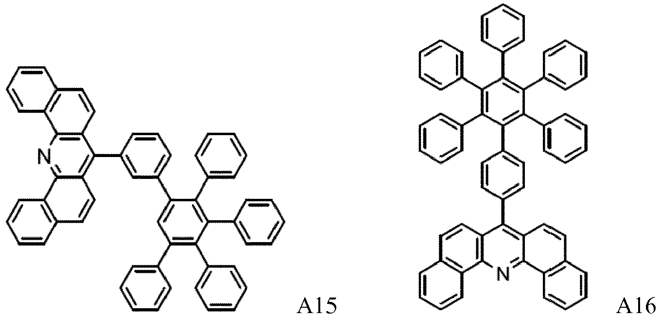

- Under electrical n-dopant, it is understood a compound which, if embedded into an electron transport matrix, improves, in comparison with the neat matrix under the same physical condictions, the electron properties of the formed semiconducting material, particularly in terms of electron injection and/or electron conductivity.
- In the context of the present invention "embedded into an electron transport matrix" means homogenously mixed with the electron transport matrix.
- The electrical n-dopant may be selected from elemental metals, metal salts, metal complexes and organic radicals.
- In one embodiment, the electrical n-dopant is selected from alkali metal salts and alkali metal complexes; preferably from lithium salts and lithium organic complexes; more preferably from lithium halides and lithium organic chelates; even more preferably from lithium fluoride, a lithium quinolinolate, lithium borate, lithium phenolate, lithium pyridinolate or from a lithium complex with a Schiff base ligand; most preferably,
- the lithium quinolinolate complex has the formula II, III or IV:

- A1 to A6 are same or independently selected from CH, CR, N, O;
- R is same or independently selected from hydrogen, halogen, alkyl or aryl or heteroaryl with 1 to 20 carbon atoms; and more preferred A1 to A6 are CH,
- the borate based organic ligand is a tetra(1H-pyrazol-1-yl)borate,
- the phenolate is a 2-(pyridin-2-yl)phenolate, a 2-(diphenylphosphoryl)phenolate, an imidazol phenolate, 2-(pyridin-2-yl)phenolate or 2-(1-phenyl-1H-benzo[d]imidazol-2-yl)phenolate,
- the pyridinolate is a 2-(diphenylphosphoryl)pyridin-3-olate,
- the lithium Schiff base has the
structure 100, 101, 102 or 103: - In another embodiment, the electrical n-dopant is a redox n-dopant.
- Under redox n-dopant, it is understood a compound which, if embedded into an electron transport matrix, increases concentration of free electrons in comparison with the neat matrix under the same physical condictions.
- The redox n-dopant may not emit light under the operation condition of an electroluminescent device, for example an OLED. In one embodiment, the redox n-dopant is selected from an elemental metal, an electrically neutral metal complex and/or an electrically neutral organic radical.
- The most practical benchmark for the strength of an n-dopant is the value of its redox potential. There is no particular limitation in terms how negative the value of the redox potential can be.
- As reduction potentials of usual electron transport matrices used in organic semiconductors are, if measured by cyclic voltammetry against ferrocene/ferrocenium reference redox couple, roughly in the range from about - 0.8 V to about - 3.1V; the practically applicable range of redox potentials for n-dopants which can effectively n-dope such matrices is in a slightly broader range, from about - 0.5 to about - 3.3 V.
- The measurement of redox potentials is practically performed for a corresponding redox couple consisting of the reduced and of the oxidized form of the same compound. In case that the redox n-dopant is an electrically neutral metal complex and/or an electrically neutral organic radical, the measurement of its redox potential is actually performed for the redox couple formed by
- (i) the electrically neutral metal complex and its cation radical formed by an abstraction of one electron from the electrically neutral metal complex, or
- (ii) the electrically neutral organic radical and its cation formed by an abstraction of one electron from the electrically neutral organic radical.
- Preferably, the redox potential of the electrically neutral metal complex and/or of the electrically neutral organic radical may have a value which is more negative than - 0.5 V, preferably more negative than - 1.2 V, more preferably more negative than - 1.7 V, even more preferably more negative than - 2.1 V, most preferably more negative than - 2.5 V, if measured by cyclic voltammetry against ferrocene/ferrocenium reference redox couple for a corresponding redox couple consisting of
- (i) the electrically neutral metal complex and its cation radical formed by an abstraction of one electron from the electrically neutral metal complex, or
- (ii) the electrically neutral organic radical and its cation formed by an abstraction of one electron from the electrically neutral organic radical.
- In a preferred embodiment, the redox potential of the n-dopant is between the value which is about 0.5 V more positive and the value which is about 0.5 V more negative than the value of the reduction potential of the chosen electron transport matrix.
Electrically neutral metal complexes suitable as redox n-dopants may be e.g. strongly reductive compelxes of some transition metals in low oxidation state. Particularly strong redox n-dopants may be selected for example from Cr(II), Mo(II) and/or W(II) guanidinate complexes such as W2(hpp)4, as described in more detail inWO2005/086251 . - Electrically neutral organic radicals suitable as redox n-dopants may be e.g. organic radicals created by supply of additional energy from their stable dimers, oligomers or polymers, as described in more detail in
EP 1 837 926 B1 ,WO2007/107306 , orWO2007/107356 .Under an elemental metal, it is understood a metal in a state of a neat metal, of a metal alloy, or in a state of free atoms or metal clusters. It is understood that metals deposited by vacuum thermal evaporation from a metallic phase, e.g. from a neat bulk metal, vaporize in their elemental form. - It is further understood that if the vaporized elemental metal is deposited together with a covalent matrix, the metal atoms and/or clusters are embedded in the covalent matrix. In other words, it is understood that any metal doped covalent material prepared by vacuum thermal evaporation contains the metal at least partially in its elemental form.
- For the use in consumer electronics, only metals containing stable nuclides or nuclides having very long halftime of radioactive decay might be applicable. As an acceptable level of nuclear stability, the nuclear stability of natural potassium can be taken.
- In one embodiment, the n-dopant may be selected from electropositive metals selected from alkali metals, alkaline earth metals, rare earth metals and metals of the first transition period Ti, V, Cr and Mn. Preferably, the n-dopant may be selected from_Li, Na, K, Rb, Cs, Mg, Ca, Sr, Ba, Sm, Eu, Tm, Yb; more preferably from Li, Na, K, Rb, Cs, Mg and Yb, even more preferably from Li, Na, Cs and Yb, most preferably from Li, Na and Yb.
- The redox dopant may be essentially non-emissive.
- According to another aspect of the invention, it is provided an electronic device comprising a first electrode, a second electrode, and arranged between the first and second electrode, a layer of the organic semiconducting material according to invention. The layer of the semiconducting material according to invention may serve as a charge injection layer or a charge transport layer or a charge generating layer. In one embodiment, the electronic device is an electroluminescent device. Preferably, the electroluminescent device is an organic light emitting diode.
- According to another aspect of the invention, it is provided an electronic device comprising at least one electroluminescent device according to any embodiment described throughout this application, preferably, the electronic device comprises the organic light emitting diode in one of embodiments described throughout this application. More preferably, the electronic device is a display device.
-
-
FIG. 1 is a cross-sectional view showing an organic light emitting diode according to an embodiment of the invention. -
FIGS. 2 and3 are cross-sectional views specifically showing a part of an organic layer of an organic light emitting diode according to an embodiment of the invention. - Hereinafter, the figures are illustrated in more detail with reference to examples. However, the present disclosure is not limited to the following figures.
-
FIGS. 1 to 3 are schematic cross-sectional views of organiclight emitting diodes FIG 1 , a structure of an organic light emitting diode according to an embodiment of the present invention and a method of manufacturing the same are as follows. The organiclight emitting diode 100 has a structure where ananode 110, a stack oforganic layers 105 including an optional hole transport region; anemission layer 130; and acathode 150 that are sequentially stacked. - A substrate may be disposed on the
anode 110 or under thecathode 150. The substrate may be selected from usual substrate used in a general organic light emitting diode and may be a glass substrate or a transparent plastic substrate. - The
anode 110 may be formed by depositing or sputtering an anode material on a substrate. The anode material may be selected from materials having a high work function that makes hole injection easy. Theanode 110 may be a reflective electrode, a transflective electrode, or a transmissive electrode. The anode material may use indium tin oxide (ITO), indium zinc oxide (IZO), tin oxide (SnO2), zinc oxide (ZnO), and the like. Or, it may be a metal such as silver (Ag), or gold (Au), or an alloy thereof. - The
anode 110 may have a monolayer or a multi-layer structure of two or more layers. - The organic
light emitting diodes emission layer 130; and a firstelectron transport layer 31 comprising a compound according to formula I. - Referring to
FIG. 2 , the hole transport region of the stack oforganic layers 105 may include at least two layered hole transport layers, and in this case, the hole transport layer contacting the emission layer (130) is defined as a secondhole transport layer 135 and a the hole transport layer contacting the anode (110) is defined as a firsthole transport layer 34. The stack oforganic layers 105 further includes two electron transport layers, namely secondelectron transport layer 33 and the firstelectron transport layer 31. The hole transport region of thestack 105 may further include at least one of a hole injection layer, a hole transport layer, an electron blocking layer, and a buffer layer. - The hole transport region of the
stack 105 may include only hole injection layer or only hole transport layer. Or, the hole transport region may have a structure where ahole injection layer 36/hole transport layer 34 orhole injection layer 36/hole transport layer 34/electron blocking layer (135) is sequentially stacked from theanode 110. - For example, the
hole injection layer 36 and theelectron injection layer 37 can be additionally included, so that an OLED may comprise ananode 110/hole injection layer 36/firsthole transport layer 34/electron blocking layer 135/emission layer 130/secondelectron transport layer 33/ firstelectron transport layer 31/electron injection layer 37/cathode 150, which are sequentially stacked. - According to another aspect of the invention, the organic electroluminescent device (400) comprises an anode (110), a hole injection layer (36), a first hole transport layer (34), optional an electron blocking layer (135), an emission layer (130), second electron transport layer (33), first electron transport layer (31), an optional electron injection layer (37), a cathode (150) wherein the layers are arranged in that order.
- The
hole injection layer 36 may improve interface properties between ITO as an anode and an organic material used for thehole transport layer 34, and is applied on a non-planarized ITO and thus planarizes the surface of the ITO. For example, thehole injection layer 36 may include a material having a median value of the energy level of its highest occupied molecular orbital (HOMO) between the work function of ITO and the energy level of the HOMO of thehole transport layer 34, in order to adjust a difference between the work function of ITO as an anode and the energy level of the HOMO of the firsthole transport layer 34. - When the hole transport region includes a
hole injection layer 36, the hole injection layer may be formed on theanode 110 by any of a variety of methods, for example, vacuum deposition, spin coating, casting, Langmuir-Blodgett (LB) method, or the like. - When hole injection layer is formed using vacuum deposition, vacuum deposition conditions may vary depending on the material that is used to form the hole injection layer, and the desired structure and thermal properties of the hole injection layer to be formed and for example, vacuum deposition may be performed at a temperature of about 100 °C to about 500 °C, a pressure of about 10-6 Pa to about 10-1 Pa, and a deposition rate of about 0.1 to about 10 nm/sec, but the deposition conditions are not limited thereto.
- When the hole injection layer is formed using spin coating, the coating conditions may vary depending on the material that is used to form the hole injection layer, and the desired structure and thermal properties of the hole injection layer to be formed. For example, the coating rate may be in the range of about 2000 rpm to about 5000 rpm, and a temperature at which heat treatment is performed to remove a solvent after coating may be in a range of about 80 °C to about 200 °C, but the coating conditions are not limited thereto.
- Conditions for forming the hole transport layer and the electron blocking layer may be defined based on the above-described formation conditions for the hole injection layer.
- A thickness of the hole transport part of the charge transport region may be from about 10 nm to about 1000 nm, for example, about 10 nm to about 100 nm. When the hole transport transport part of the charge transport region includes the hole injection layer and the hole transport layer, a thickness of the hole injection layer may be from about 10 nm to about 1000 nm, for example about 10 nm to about 100 nm and a thickness of the hole transport layer may be from about 5 nm to about 200 nm, for example about 10 nm to about 150 nm. When the thicknesses of the hole transport part of the charge transport region, the HIL, and the HTL are within these ranges, satisfactory hole transport characteristics may be obtained without a substantial increase in driving voltage.
- Hole transport matrix materials used in the hole transport region are not particularly limited. Preferred are covalent compounds comprising a conjugated system of at least 6 delocalized electrons. The term "covalent compound" is in more detail explained below, in the paragraph regarding the second electron transport matrix. Typical examples of hole transport matrix materials which are widely used in hole transport layers are polycyclic aromatic hydrocarbons, triaryl amine compounds and heterocyclic aromatic compounds. Suitable ranges of frontier orbital energy levels of hole transport matrices useful in various layer of the hole transport region are well-known. In terms of the redox potential of the redox couple HTL matrix/ cation radical of the HTL matrix, the preferred values (if measured for example by cyclic voltammetry against ferrocene/ferrocenium redox couple as reference) may be in the range 0.0 - 1.0 V, more preferably in the range 0.2 - 0.7 V, even more preferably in the range 0.3 - 0.5 V.
- The hole transport region of the stack of organic layers may further include a charge-generating material to improve conductivity, in addition to the materials as described above. The charge-generating material may be homogeneously or non-homogeneously dispersed in the hole transport region.
- The charge-generating material may be, for example, a p-dopant. The p-dopant may be one of a quinone derivative, a metal oxide, and a cyano group-containing compound, but is not limited thereto. Non-limiting examples of the p-dopant are quinone derivatives such as tetracyanoquinonedimethane (TCNQ), 2,3,5,6-tetrafluoro-tetracyano-1,4-benzoquinonedimethane (F4-TCNQ), and the like; metal oxides such as tungsten oxide, molybdenum oxide, and the like; and cyano-containing compounds such as compound HT-D1 below.

- The hole transport part of the charge transport region may further include a buffer layer.
- The buffer layer may compensate for an optical resonance distance of light according to a wavelength of the light emitted from the EML, and thus may increase efficiency.
- The emission layer (EML) may be formed on the hole transport region by using vacuum deposition, spin coating, casting, LB method, or the like. When the emission layer is formed using vacuum deposition or spin coating, the conditions for deposition and coating may be similar to those for the formation of the hole injection layer, though the conditions for the deposition and coating may vary depending on the material that is used to form the emission layer. The emission layer may include an emitter host (EML host) and an emitter dopant (further only emitter).
- The emitter may be a red, green, or blue emitter.
- In one embodiment, the emitter host is an anthracene matrix compound represented by
formula 400 below:
- In
formula 400, Ar111 and Ar112 may be each independently a substituted or unsubstituted C6-C60 arylene group; Ar113 to Ar116 may be each independently a substituted or unsubstituted C1-C10 alkyl group or a substituted or unsubstituted C6-C60 aryl group; and g, h, i, and j may be each independently an integer from 0 to 4. In some embodiments, Ar111 and Ar112 informula 400 may be each independently one of a phenylene group, a naphthylene group, a phenanthrenylene group, or a pyrenylene group; or a phenylene group, a naphthylene group, a phenanthrenylene group, a fluorenyl group, or a pyrenylene group, each substituted with at least one of a phenyl group, a naphthyl group, or an anthryl group. - In
formula 400, g, h, i, and j may be each independently an integer of 0, 1, or 2.
Informula 400, Ar113 to Ar116 may be each independently one of - a C1-C10 alkyl group substituted with at least one of a phenyl group, a naphthyl group, or an anthryl group;
- a phenyl group, a naphthyl group, an anthryl group, a pyrenyl group, a phenanthrenyl group, or a fluorenyl group;
- a phenyl group, a naphthyl group, an anthryl group, a pyrenyl group, a phenanthrenyl group, or
- a fluorenyl group, each substituted with at least one of a deuterium atom, a halogen atom, a hydroxyl group, a cyano group, a nitro group, an amino group, an amidino group, a hydrazine group, a hydrazone group, a carboxyl group or a salt thereof,
- a sulfonic acid group or a salt thereof,
- a phosphoric acid group or a salt thereof,
- a C1-C60 alkyl group, a C2-C60 alkenyl group, a C2-C60 alkynyl group, a C1-C60 alkoxy group, a phenyl group, a naphthyl group, an anthryl group, a pyrenyl group, a phenanthrenyl group, or
- a fluorenyl group; or


- Wherein in the formulas (Y2) and (Y3), X is selected form an oxygen atom and a sulfur atom, but embodiments of the invention are not limited thereto.
- In the formula (Y2), any one of R11 to R14 is used for bonding to Ar111. R11 to R14 that are not used for bonding to Arm and R15 to R20 are the same as R1 to R8.
- In the formula (Y3), any one of R21 to R24 is used for bonding to Ar111. R21 to R24 that are not used for bonding to Arm and R25 to R30 are the same as R1 to R8.
- Preferably, the EML host comprises between one and three heteroatoms selected from the group consisting of N, O or S. More preferred the EML host comprises one heteroatom selected from S or O.
- According to a further aspect of the invention, the emitter host respectively has a reduction potential which, if measured under the same conditions by cyclic voltammetry against Fc/Fc+ in tetrahydrofuran, has a value more negative than the respective value obtained for 7-([1,1'-biphenyl]-4-yl)dibenzo[c,h]acridine, preferably more negative than the respective value for 9,9',10,10'-tetraphenyl-2,2'-bianthracene, more preferably more negative than the respective value for 2,9-di([1,1'-biphenyl]-4-yl)-4,7-diphenyl-1,10-phenanthroline, even more preferably more negative than the respective value for 2,4,7,9-tetraphenyl-1,10-phenanthroline, even more preferably more negative than the respective value for 9,10-di(naphthalen-2-yl)-2-phenylanthracene, even more preferably more negative than the respective value for 2,9-bis(2-methoxyphenyl)-4,7-diphenyl-1,10-phenanthroline, most preferably more negative than the respective value for 9,9'-spirobi[fluorene]-2,7-diylbis(diphenylphosphine oxide).
- The emitter is mixed in a small amount to cause light emission, and may be generally a material such as a metal complex that emits light by multiple excitation into a triplet or more. The emitter may be, for example an inorganic, organic, or organometallic compound, and one or more kinds thereof may be used.
- The emitter may be a fluorescent emitter, for example ter-fluorene, the structures are shown below. 4.4'-bis(4-diphenyl amiostyryl)biphenyl (DPAVBi), 2,5,8,11-tetra-tert-butyl perylene (TBPe), and Compound 4 below are examples of fluorescent blue emitters.
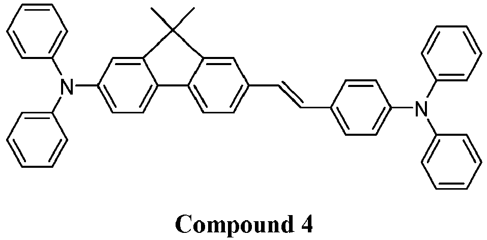
- According to another aspect, the organic semiconductor layer comprising a compound of formula I is arranged between a fluorescent blue emission layer and the cathode electrode.
- The emitter may be a phosphorescent emitter, and examples of the phosphorescent emitters may be organometallic compounds including Ir, Pt, Os, Ti, Zr, Hf, Eu, Tb, Tm, Fe, Co, Ni, Ru, Rh, Pd, or a combination thereof. The phosphorescent emitter may be, for example a compound represented by formula Z, but is not limited thereto:
L2MX (Z).
- In formula Z, M is a metal, and L and X are the same or different, and are a ligand to form a complex compound with M.
- The M may be, for example Ir, Pt, Os, Ti, Zr, Hf, Eu, Tb, Tm, Fe, Co, Ni, Ru, Rh, Pd or, in a polynuclear complex,a combination thereof, and the L and X may be, for example, a bidendate ligand.
- A thickness of the emission layer may be about 10 nm to about 100 nm, for example about 20 nm to about 60 nm. When the thickness of the emission layer is within these ranges, the emission layer may have improved emission characteristics without a substantial increase in a driving voltage.
- Next, the electron transport region of the stack of
organic layers 105 is disposed on the emission layer. - The electron transport region of the stack of organic layers includes at least the first electron transport layer. The electron transport region of the stack of organic layers may further include an electron injection layer and/or the second electron transport layer. At least the first electron transport layer comprises the n-doped semiconducting material according to one of its various embodiments.
- For example, the electron transport region of the stack of organic layers may have a structure of the first electron transport layer/second electron transport layer/electron injection layer but is not limited thereto. For example, an organic light emitting diode according to an embodiment of the present invention includes at least two electron transport layers in the electron transport region of the stack of
organic layers 105, and in this case, the electron transport layer contacting the emission layer is defined as the secondelectron transport layer 33. - The electron transport layer may include two or more different electron transport matrix compounds.
- Various embodiments of the electron transport region in the device according to invention, e.g. devices comprising hole blocking layers, electron injecting layers, may comprise a second electron transport matrix compound.
- Second electron transport matrix is not particularly limited. Similarly as other materials which are in the inventive device comprised outside the emitting layer, the second electron transport matrix may not emit light.
- According to one embodiment, the second electron transport matrix can be an organic compound, an organometallic compound, or a metal complex.
- According to one embodiment, the second electron transport matrix may be a covalent compound comprising a conjugated system of at least 6 delocalized electrons. Under a covalent material in a broadest possible sense, it might be understood a material, wherein at least 50 % of all chemical bonds are covalent bonds, wherein coordination bonds are also considered as covalent bonds. In the present application, the term encompasses in the broadest sense all usual electron transport matrices which are predominantly selected from organic compounds but also e.g. from compounds comprising structural moieties which do not comprise carbon, for example substituted 2,4,6-tribora-1,3,5 triazines, or from metal complexes, for example aluminium tris(8-hydroxyquinolinolate).
- The molecular covalent materials can comprise low molecular weight compounds which may be, preferably, stable enough to be processable by vacuum thermal evaporation (VTE). Alternatively, covalent materials can comprise polymeric covalent compounds, preferably, compounds soluble in a solvent and thus processable in form of a solution. It is to be understood that a polymeric substantially covalent material may be crosslinked to form an infinite irregular network, however, it is supposed that such crosslinked polymeric substantially covalent matrix compound still comprises both skeletal as well as peripheral atoms. Skeletal atoms of the covalent compound are covalently bound to at least two neighbour atoms. Other atoms of the covalent compound are peripheral atoms which are covalently bound with a single neighbour atom. Inorganic infinite crystals or fully crosslinked networks having partly covalent bonding but substantially lacking peripheral atoms, like silicon, germanium, gallium arsenide, indium phosphide, zinc sulfide, silicate glass etc. are not considered as covalent matrices in the sense of present application, because such fully crosslinked covalent materials comprise peripheral atoms only on the surface of the phase formed by such material. A compound comprising cations and anions is still considered as covalent, if at least the cation or at least the anion comprises at least ten covalently bound atoms.
- Preferred examples of covalent second electron transport matrix compounds are organic compounds, consisting predominantly from covalently bound C, H, O, N, S, which may optionally comprise also covalently bound B, P, As, Se. In one embodiment, the second electron transport matrix compound lacks metal atoms and majority of its skeletal atoms is selected from C, O, S, N.
- In another embodiment, the second electron transport matrix compound comprises a conjugated system of at least six, more preferably at least ten, even more preferably at least fourteen delocalized electrons.
- Examples of conjugated systems of delocalized electrons are systems of alternating pi- and sigma bonds. Optionally, one or more two-atom structural units having the pi-bond between its atoms can be replaced by an atom bearing at least one lone electron pair, typically by a divalent atom selected from O, S, Se, Te or by a trivalent atom selected from N, P, As, Sb, Bi. Preferably, the conjugated system of delocalized electrons comprises at least one aromatic or heteroaromatic ring adhering to the Hückel rule. Also preferably, the second electron transport matrix compound may comprise at least two aromatic or heteroaromatic rings which are either linked by a covalent bond or condensed.
- In one of specific embodiments, the second electron transport matrix compound comprises a ring consisting of covalently bound atoms and at least one atom in the ring is phosphorus.
- In a more preferred embodiment, the phosphorus-containing ring consisting of covalently bound atoms is a phosphepine ring.
- In another preferred embodiment, the covalent matrix compound comprises a phosphine oxide group. Also preferably, the substantially covalent matrix compound comprises a heterocyclic ring comprising at least one nitrogen atom. Examples of nitrogen containing heterocyclic compounds which are particularly advantageous as second electron transport matrix compound for the inventive device are matrices comprising, alone or in combination, pyridine structural moieties, diazine structural moieties, triazine structural moieties, quinoline structural moieties, benzoquinoline structural moieties, quinazoline structural moieties, acridine structural moieties, benzacridine structural moieties, dibenzacridine structural moieties, diazole structural moieties and benzodiazole structural moieties.
- The second matrix compound may have a molecular weight (Mw) of ≥ 400 to ≤ 850 g / mol, preferably ≥ 450 to ≤ 830 g / mol. If the molecular weight is selected in this range, particularly reproducible evaporation and deposition can be achieved in vacuum at temperatures where good long-term stability is observed.
- Preferably, the second matrix compound may be essentially non-emissive.
- According to another aspect, the reduction potential of the second electron transport compound may be selected more negative than -2.2 V and less negative than -2.35 V against Fc/Fc+ in tetrahydrofuran, preferably more negative than -2.25 V and less negative than -2.3 V.
- According to one embodiment, the first and the second matrix compound may be selected different, and
- the second electron transport layer consist of a second matrix compound; and
- the first electron transport layer consist of the first matrix compound of formula (I), and an electrical n-dopant, preferably an alkali metal salt or an alkali metal organic complex.
- Preferably, the first and second electron transport layer may be essentially non-emissive.
- According to another embodiment, the second electron transport layer can be in direct contact with the emission layer.
- According to another embodiment, the first electron transport layer can be in direct contact with the second electron transport layer.
- According to another embodiment, the second electron transport layer can be contacting sandwiched between the emission layer and the first electron transport layer.
- According to another embodiment, the first electron transport layer can be in direct contact with the electron injection layer.
- According to another embodiment, the first electron transport layer can be contacting sandwiched between the second electron transport layer and the electron injection layer.
- According to another embodiment, the first electron transport layer can be in direct contact with the cathode electrode.
- According to another embodiment, the first electron transport layer can be contacting sandwiched between the second electron transport layer and the cathode layer.
- According to another embodiment, the second electron transport layer can be contacting sandwiched between the emission layer and the first electron transport layer, and the first electron transport layer can be contacting sandwiched between the second electron transport layer and the electron injection layer.
- The formation conditions of the first
electron transport layer 31, secondelectron transport layer 33, andelectron injection layer 37 of the electron transport region of the stack of organic layers refer to the formation conditions of the hole injection layer. - The thickness of the first electron transport layer may be from about 2 nm to about 100 nm, for example about 3 nm to about 30 nm. When the thickness of the first electron transport layer is within these ranges, the first electron transport layer may have improved electron transport auxiliary ability without a substantial increase in driving voltage.
- A thickness of the second electron transport layer may be about 10 nm to about 100 nm, for example about 15 nm to about 50 nm. When the thickness of the electron transport layer is within these ranges, the electron transport layer may have satisfactory electron transporting ability without a substantial increase in driving voltage.
- According to another aspect of the invention, the organic electroluminescent device further comprises an electron injection layer between the second electron transport layer and the cathode.
- The electron injection layer (EIL) 37 may facilitate injection of electrons from the
cathode 150. - According to another aspect of the invention, the
electron injection layer 37 comprises: - (i) an electropositive metal selected from alkali metals, alkaline earth metals and rare earth metals in substantially elemental form, preferably selected from Li, Na, K, Rb, Cs, Mg, Ca, Sr, Ba, Eu and Yb, more preferably from Li, Na, Mg, Ca, Sr and Yb, even more preferably from Li and Yb, most preferably Yb; and/or
- (ii) an alkali metal complex and/or alkali metal salt, preferably the Li complex and/or salt, more preferably a Li quinolinolate, even more preferably a lithium 8-hydroxyquinolinolate, most preferably the alkali metal salt and/or complex of the second electron transport layer is idencial with the alkali metal salt and/or complex of the injection layer.
- The electron injection layer may include at least one selected from LiF, NaCl, CsF, Li2O, and BaO.
- A thickness of the EIL may be from about 0.1 nm to about 10 nm, or about 0.3 nm to about 9 nm. When the thickness of the electron injection layer is within these ranges, the electron injection layer may have satisfactory electron injection ability without a substantial increase in driving voltage.
- A material for the
cathode 150 may be a metal, an alloy, or an electrically conductive compound that have a low work function, or a combination thereof. Specific examples of the material for thecathode 150 may be lithium (Li), magnesium (Mg), aluminum (Al), aluminum-lithium (Al-Li), calcium (Ca), magnesium-indium (Mg-In), magnesium-silver (Mg-Ag), etc. In order to manufacture a top-emission light-emitting device having areflective anode 110 deposited on a substrate, thecathode 150 may be formed as a transmissive electrode from, for example, indium tin oxide (ITO) or indium zinc oxide (IZO). - Hereinafter, the embodiments are illustrated in more detail with reference to examples. However, the present disclosure is not limited to the following examples.
- Triazine compounds of formula I may be synthesized in accordance with the methods described in
PCT-KR2015-012551 -
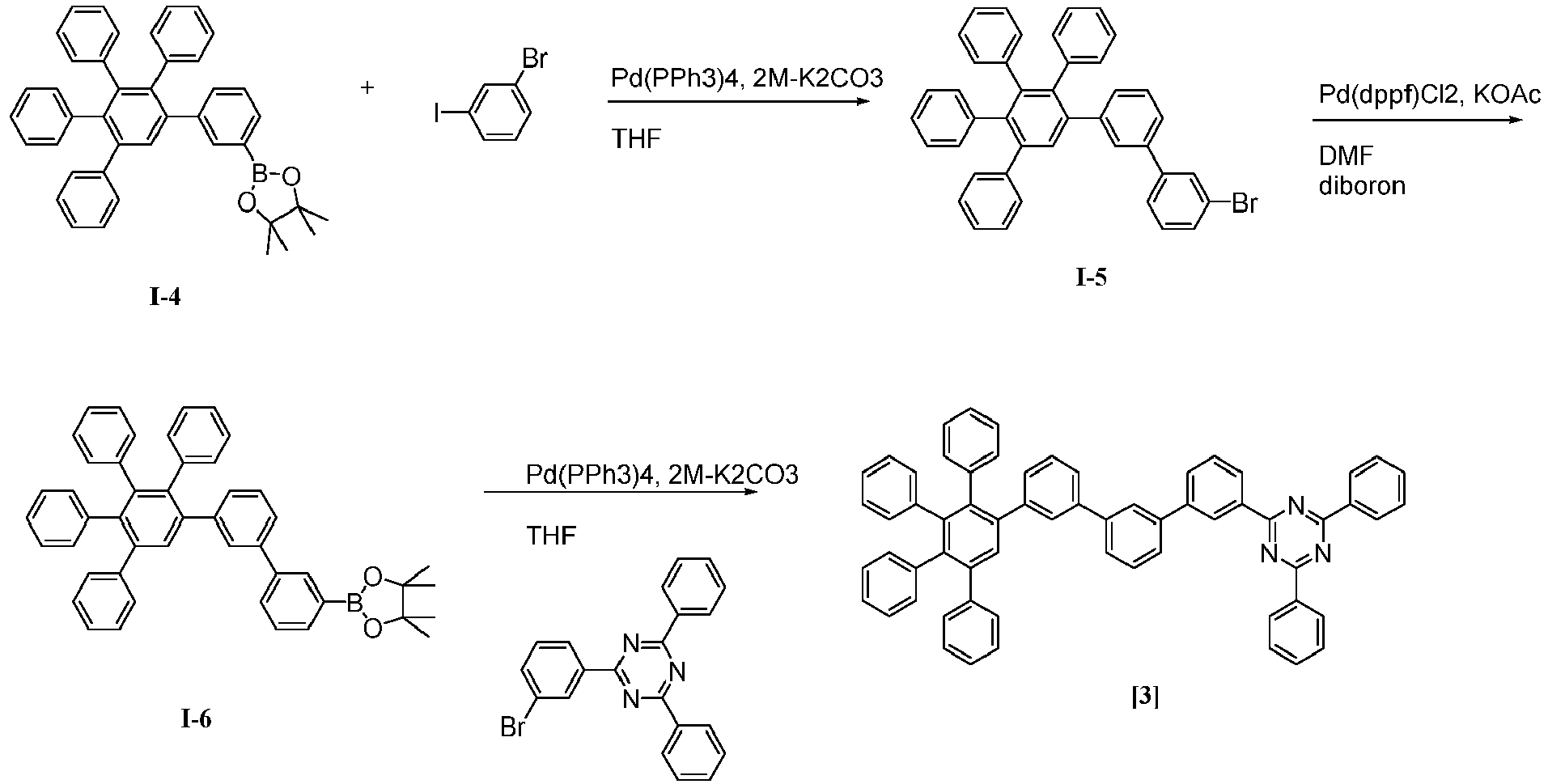
- 13 g of an intermediate I-5 (61 %) was obtained in the same synthesis method as the synthesis method of the compound 1 by using the intermediate I-4 (20.4 g, 34.92 mmol) and 1-bromo-3-iodobenzene (16.5 g, 52.39 mmol) under a nitrogen environment.
- 10 g of an intermediate I-6 (74 %) was obtained in the same synthesis method as the synthesis method of the intermediate I-4 by using the intermediate I-5 (12.6 g, 20.54 mmol) under a nitrogen environment.
- 8.7 g of compound A6 (in the scheme referred as [3]) was obtained in 68 % yield by using the intermediate I-6 (10 g, 15.2 mmol) and 2-(3-bromophenyl)-4,6-diphenyl-1,3,5-triazine (7.9 g, 18.32 mmol). These reagents were dissolved in 250 mL tetrahydrofuran under a nitrogen environment, tetrakis(triphenylphosphine)palladium (0.9 g, 0.75 mmol) was added thereto, and the mixture was stirred. Then, potassium carbonate saturated in water (5.2 g, 37 mmol) was added thereto, and the mixture was heated and refluxed at 80°C for 24 hours. When the reaction was complete, water was added to the reaction solution, dichloromethane was used to perform an extraction, an anhydrous MgSO4 was used to remove moisture therefrom, and a resultant therefrom was filtered and concentrated under a reduced pressure. This obtained residue was separated and purified through column chromatography.
- LC Mass (theoretical value: 842.04 g/mol, measured value: M+H+ = 843.03 g/mol)
- The benzoquinazoline compound A9 was prepared analogously. Physical properties of tested compounds of formula (I) are summarized in Table 1.
- Dibenzoacridine compounds of formula I may be synthesized in accordance with the methods described in
WO2011/154131A1 . - Another alternative is demonstrated in Synthesis example 2. The procedure is generally applicable for the synthesis of compounds comprising the hexaphenylbenzene structural moiety.
-

- A three necked 250-mL round bottom flask is purged with N2. Under a constant flow of N2 7-(4-bromophenyl)dibenzo[c,h]acridine (10.0 g, 23.0 mmol), phenylacetylene (4.70 g, 46.0 mmol, 2.0 eq.), and bis (triphenylphosphine)-palladium chloride (3.23 g, 4.6 mmol, 0.2 eq.) were introduced, followed by a 1M-solution of tetrabutylammonium fluoride in THF (70 mL). The resulting mixture was warmed up to reflux and reacted for 2h. After completion of the reaction, MeOH (70 mL) was added, and the solution was left to cool down to room temperature. The precipitate formed upon cooling was collected by filtration, washed with MeOH (2 x 50 mL), then hexane (3 x 50 mL), and finally dried under vacuum at 40°C.
- Yield: about 7.0 g (about 67%, yellowish solid).
-

- A three necked 100-mL round bottom flask was charged with 7-(4-(phenylethynyl)phenyl)dibenzo[c,h]acridine (6.8 g, 14.9 mmol), 2,3,4,5-tetraphenylcyclopenta-2,4-dienone (6.31 g, 16.4 mmol, 1.1 eq.), and benzophenone (35 g as molten solvent). After degassing the solids with N2, the resulting mixture was warmed up to 300°C. After lh of reflux at 300°C, gas evolution had stopped and the mixture was hence cooled down to ca. 80°C. Toluene (100 mL), was added, and the resulting precipitate was filtered off and washed with toluene (2 x 40 mL), followed by hexane (2 x 40 mL). The solid was then purified by trituration in hot chlorobenzene (60 mL), followed by trituration in hot MeOH (60 mL). After filtration and drying under vacuum at 120°C, the desired was isolated as a yellowish powder.
- Yield: about 6.8 g (about 56%, yellowish solid).
- The benzoacridine compound A18 was prepared analogously. In Table 1 are summarized dibenzoacridine compounds of formula I and their starting material, yield, m/z, glass transition temperature, reduction potential against Fc/Fc+ in tetrahydrofuran.
Table 1 Comp. I: Starting materials Structure of compound I Yield [%] Tg [°C] Redox potential against Fc/Fc+ [V] A1 

62% 175 -2.25 A2 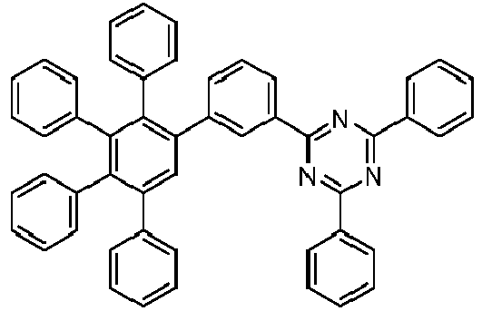
138 -2.20 A3 
135 -2.20 A4 
140 -2.22 A5 

86% 165 -2.29 A6 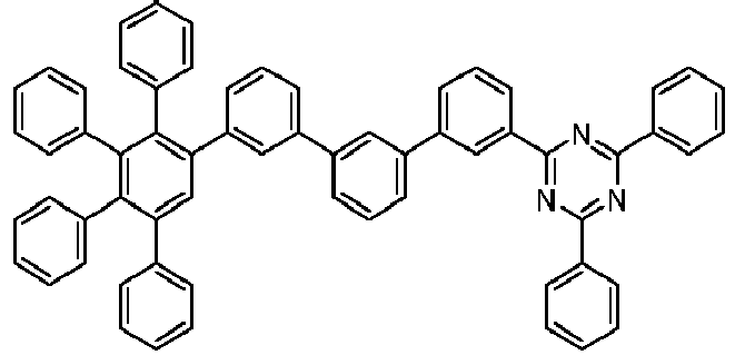
139 -2.18 A7 
147 -2.15 A8 
147 -2.18 A9 
144 -2.25 A10 
149 -2.14 A12 - -2.18 A13 - -2.23 A15 58% 159 -2.29 A16 
Not obse rved -2.31 A17 50% 175 - A18 
Not obse rved -2.25 - The model top emitting blue fluorescent OLED is described below. It was prepared using auxiliary materials F1, F2, F3, F4, F5, F6 and PD-2:


- A glass substrate was cut to a size of 50 mm x 50 mm x 0.7 mm, ultrasonically cleaned with isopropyl alcohol for 5 minutes and then with pure water for 5 minutes, and cleaned again with UV ozone for 30 minutes, to prepare a first electrode. 100 nm Ag were deposited as anode at a pressure of 10-5 to 10-7 mbar.
- Then, 92 wt.-% F1 with 8 wt.-% PD2 were vacuum deposited on the ITO electrode, to form a HIL having a thickness of 10 nm. Then, undoped F1 was vacuum deposited on the HIL, to form a HTL having a thickness of 122 nm.
Then, F2 was vacuum deposited on the HTL, to form an electron blocking layer (EBL) having a thickness of 5 nm. - Then, 97 wt.-% F3 as EML host and 3 wt.-% blue dopant NUBD370 (Sun Fine Chemicals) were deposited on the HTL, to form a blue-emitting EML with a thickness of 20 nm.
- Then the second
electron transport layer 33, if present, is formed with a thickness of 5 nm by depositing compound A6, and the firstelectron transport layer 31 is formed either directly on the emission layer or on the second electron transport layer according. If the first electron transport layer is in direct contact with the emission layer, the thickness is 36 nm. If the first electron transport layer is deposited on top of the second electron transport layer, the thickness is 31 nm. - The first electron transport layer comprises 50 wt.-% matrix compound and 50 wt.-% of LiQ. The composition is shown in Table 2.
- Then the
electron injection layer 37 is formed on theelectron transport layer 31 by depositing LiQ with a thickness of 1.5 nm or Yb with a thickness of 2 nm. - The cathode was evaporated at ultra-high vacuum of 10-7 mbar. Therefore, a thermal single co-evaporation of one or several metals was performed with a rate of 0, 1 to 10 nm/s (0.01 to 1 Å/s) in order to generate a homogeneous cathode with a thickness of 5 to 1000 nm. The cathode was formed from 13 nm magnesium silver alloy (90:10 vol.-%) or from 11 nm Ag.
- A cap layer of F1 was formed on the cathode with a thickness of 60 nm in case of MgAg cathode and 75 nm in case of Ag cathode.
- To assess the performance of the inventive examples compared to the prior art, the current efficiency is measured under ambient conditions (20°C). Operational voltage measurements are performed using a Keithley 2400 sourcemeter, and reported in V at standard current density 10 mA/cm2 for top emission devices. For bottom emission devices, the standard current density is usually 15 mA/cm2. A calibrated spectrometer CAS140 from Instrument Systems is used for measurement of CIE coordinates and brightness in Candela. Lifetime LT of the device is measured at ambient conditions (20°C) and standard current density 10 mA/cm2 or 15 mA/cm2, using a Keithley 2400 sourcemeter, and recorded in hours. The brightness of the device is measured using a calibrated photo diode. The lifetime LT is defined as the time till the brightness of the device is reduced to 97 % of its initial value.
- The light output in external efficiency EQE and power efficiency Peff (lm/W) are determined at 10 mA/cm2 for top emission devices.
- To determine the efficiency EQE in % the light output of the device is measured using a calibrated photodiode.
- To determine the power efficiency in lm/W, in a first step the luminance in candela per square meter (cd/m2) is measured with an array spectrometer CAS140 CT from Instrument Systems which has been calibrated by Deutsche Akkreditierungsstelle (DAkkS). In a second step, the luminance is then multiplied by π and divided by the voltage and current density.
- In bottom emission devices, the emission is predominately Lambertian and quantified in percent external quantum efficiency (EQE) and power efficiency in 1m/W. The auxiliary compounds F4-F6 served as state-of-art references; the results in terms of operational voltage U, and current efficiency Ceff are shown in Table 2.
Table 2: Performance at 10 mA/cm2 of top emission devices comprising a second ETL (33), a first ETL (34) and a lithium organic complex, and an EIL (37) second ETL first ETL EIL Cathode U(V) Ceff (cd/A) Comparative device 1 - F4:LiQ LiQ Mg:Ag 3.39 7.2 Device 1 - A15:LiQ Yb Ag 3.71 9.2 Device 2 - A5:LiQ Yb Ag 3.56 9.2 Comparative device 2 A6 F5:LiQ LiQ Mg:Ag 3.41 6.5 Device 3 A6 A16:LiQ Yb Ag 3.77 9.2 Device 4 A6 A15:LiQ Yb Ag 3.78 9.1 Comparative device 3 F5 F6:LiQ LiQ Mg:Ag 3.34 6.8 - As it may be taken from the Table 2, tested compounds of formula (I) implemented in a state-of-art semiconducting material doped with LiQ showed better results (highlighted in boldface letters) in terms of improved current efficiency than the state-of-art matrix compounds F4, F5 and F6 used as reference.
- While this invention has been described in connection with what is presently considered to be practical exemplary embodiments, it is to be understood that the invention is not limited to the disclosed embodiments, but, on the contrary, is intended to cover various modifications and equivalent arrangements included within the spirit and scope of the appended claims. Therefore, the aforementioned embodiments should be understood to be exemplary but not limiting the present invention in any way.

Claims (15)
- An organic semiconducting material comprising at least one electron transport matrix and at least one electrical n-dopant, wherein the electron transport matrix comprises at least one first matrix compound according to Chemical Formula I:
 A1, A2, A3 and A4 is independently selected from single bond, an unsubstituted or substituted C6 to C30 arylene and an unsubstituted or substituted C1 to C30 heteroarylene;A5 is selected from an unsubstituted or substituted C6 to C40 aryl group and/or from an unsubstituted or substituted C2 to C40 heteroaryl group;R1 to R5 are independently a substituted or unsubstituted C6 to C30 aryl group, a substituted or unsubstituted C2 to C30 heteroaryl group;a to e are independently an integer of 0 or 1 and 4 ≤ a+b+c+d+e ≤ 5;wherein, in formula (I), in the substituted group, at least one hydrogen is replaced by(i) deuterium,(ii) a halogen,(iii) a C2 to C60 tertiary amino group, wherein the nitrogen atom of the tertiary amino group is substituted with two independently selected C1 to C30 hydrocarbyl groups or_the nitrogen atom of the C2 to C60 tertiary amino group_forms a C1 to C30 heterocyclic group,(iv) a C2 to C60 phosphine oxide group, wherein the phosphorus atom of the phosphine oxide group is substituted with two C1 to C30 groups independently selected from hydrocarbyl, halogenated hydrocarbyl and hydrocarbyloxy or the phosphorus atom of the phosphine oxide group forms a C1 to C30 heterocyclic group,(v) a C1 to C22 silyl group,(vi) a C1 to C30 alkyl group,(vii) a C1 to C10 alkylsilyl group,(viii) a C6 to C22 arylsilyl group,(ix) a C3 to C30 cycloalkyl group,(x) a C2 to C30 heterocycloalkyl group,(xi) a C6 to C30 aryl group,(xii) a C2 to C30 heteroaryl group,(xiii) a C1 to C20 alkoxy group,(xiv) a C1 to C30 perfluoro-hydrocarbyl group,(xv) a C1 to C10 trifluoroalkyl group, or(xvi) a cyano group.
 - The organic semiconducting material according to claim 1, wherein the electrical n-dopant is selected from elemental metals, metal salts, metal complexes and organic radicals.
- The organic semiconducting material according to claim 1 or 2, wherein the electrical n-dopant is selected from alkali metal salts and alkali metal complexes; preferably from lithium salts and lithium organic complexes; more preferably from lithium halides and lithium organic chelates; even more preferably from lithium fluoride, a lithium quinolinolate, lithium borate, lithium phenolate, lithium pyridinolate or from a lithium complex with a Schiff base ligand; most preferably,- the lithium quinolinolate complex has the formula II, III or IV:
 A1 to A6 are same or independently selected from CH, CR, N, O;R is same or independently selected from hydrogen, halogen, alkyl or aryl or heteroaryl with 1 to 20 carbon atoms; and more preferred A1 to A6 are CH,- the borate based organic ligand is a tetra(1H-pyrazol-1-yl)borate,- the phenolate is a 2-(pyridin-2-yl)phenolate, a 2-(diphenylphosphoryl)phenolate, an imidazol phenolate, 2-(pyridin-2-yl)phenolate or 2-(1-phenyl-1H-benzo[d]imidazol-2-yl)phenolate,- the pyridinolate is a 2-(diphenylphosphoryl)pyridin-3-olate,- the lithium Schiff base has the structure 100, 101, 102 or 103:
- The organic semiconducting material according to any of the preceding claims 1 to 3, wherein the electrical n-dopant is a redox n-dopant.
- The organic semiconducting material according to any of the preceding claims 1 to 4, wherein the redox n-dopant is selected from an elemental metal, an electrically neutral metal complex and/or an electrically neutral organic radical.
- The organic semiconducting material according to any of the preceding claims 1 to 5, wherein the electrically neutral metal complex and/or the electrically neutral organic radical, has a redox potential which has a value which is more negative than - 0.5 V, preferably more negative than - 1.2 V, more preferably more negative than - 1.7 V, even more preferably more negative than - 2.1 V, most preferably more negative than - 2.5 V, if measured by cyclic voltammetry against ferrocene/ferrocenium reference redox couple.
- The organic semiconducting material according to any of the preceding claims 1 to 6, wherein the redox n-dopant is an electropositive elemental metal selected from alkali metals, alkaline earth metals, rare earth metals, and transition metals Ti, V, Cr and Mn; preferably from Li, Na, K, Rb, Cs, Mg, Ca, Sr, Ba, Sm, Eu, Tm, Yb; more preferably from Li, Na, K, Rb, Cs, Mg and Yb, even more preferably from Li, Na, Cs and Yb, most preferably from Li, Na and Yb.
- The organic semiconducting material according to any of the preceding claims 1 to 7, wherein the first matrix compound is a compound according to Chemical Formula (Ia)
 Ar1 is selected from C6 to C12 aryl and C1 to C11 heteroaryl; andR1 to R5 are independently a substituted or unsubstituted C6 to C30 aryl group, a substituted or unsubstituted C2 to C30 heteroaryl group;a to e are independently an integer of 0 or 1 and 4 ≤ a+b+c+d+e ≤ 5;L is a single bond, a substituted or unsubstituted C6 to C30 arylene group, or a substituted or unsubstituted C2 to C30 heteroarylene group;ET is a unsubstituted C6 to C40 aryl or C5 to C40 heteroaryl group; or a substituted C6 to C40 aryl or C5 to C40 heteroaryl group,wherein, in formula (Ia), in the substituted group, at least one hydrogen is replaced by(i) deuterium,(ii) a halogen,(iii) a C2 to C60 tertiary amino group, wherein the nitrogen atom of the C2 to C60 tertiary amino group is substituted with two independently selected C1 to C30 hydrocarbyl groups or forms a C1 to C30 heterocyclic group,(iv) a C2 to C60 phosphine oxide group, wherein the phosphorus atom of the phosphine oxide group is substituted with two C1 to C30 groups independently selected from hydrocarbyl, halogenated hydrocarbyl and hydrocarbyloxy or the phosphorus atom of the phosphine oxide group forms a C1 to C30 heterocyclic group,(v) a C1 to C22 silyl group,(vi) a C1 to C30 alkyl group,(vii) a C1 to C10 alkylsilyl group,(viii) a C6 to C22 arylsilyl group,(ix) a C3 to C30 cycloalkyl group,(x) a C2 to C30 heterocycloalkyl group,(xi) a C6 to C30 aryl group,(xii) a C2 to C30 heteroaryl group,(xiii) a C1 to C20 alkoxy group,(xiv) a C1 to C30 perfluoro-hydrocarbyl group,(xv) a C1 to C10 trifluoroalkyl group, or(xvi) a cyano group.
 - The organic semiconducting material according to any of the preceding claims 1 to 8, wherein the first matrix compound is a compound according to Chemical Formula (Ib)
 X1 to X11 are independently, N, C, or CRa;Ra is independently, hydrogen, deuterium, a C1 to C30 alkyl group, a C3 to C30 cycloalkyl group, a C6 to C30 aryl group, a C6 to C30 diarylamine group, a C1 to C30 alkoxy group, a C3 to C21 silyl group, a C3 to C21 silyloxy group, a C1 to C30 alkylthiol group, a C6 to C30 arylthiol group, a halogen, a C1 to C30 halogenated hydrocarbyl group, a cyano group;R1 to R5 are independently a substituted or unsubstituted C6 to C30 aryl group, a substituted or unsubstituted C2 to C30 heteroaryl group;a to e are independently an integer of 0 or 1 and 4 ≤ a+b+c+d+e ≤ 5,L is a single bond, a substituted or unsubstituted C6 to C30 arylene group, a substituted or unsubstituted C2 to C30 heteroarylene group, andET is a unsubstituted C6 to C40 aryl or C2 to C40 heteroaryl group, or a substituted C6 to C40 aryl or C2 to C40 heteroaryl group;wherein, in formula (Ib), in the substituted group, at least one hydrogen is replaced by(i) deuterium,(ii) a halogen,(iii) a C1 to C60 tertiary amino group, wherein the nitrogen atom of the C2 to C60 tertiary amino group is substituted with two independently selected C1 to C30 hydrocarbyl groups or forms a C1 to C30 heterocyclic group, a C2 to C60 phosphine oxide group, wherein the phosphorus atom of the phosphine oxide group is substituted with two C1 to C30 groups independently selected from hydrocarbyl, halogenated hydrocarbyl and hydrocarbyloxy or the phosphorus atom of the phosphine oxide group forms a C1 to C30 heterocyclic group,(iv) a C1 to C22 silyl group,(v) a C1 to C30 alkyl group,(vi) a C1 to C10 alkylsilyl group,(vii) a C6 to C22 arylsilyl group,(viii) a C3 to C30 cycloalkyl group,(ix) a C2 to C30 heterocycloalkyl group,(x) a C6 to C30 aryl group,(xi) a C2 to C30 heteroaryl group,(xii) a C1 to C20 alkoxy group,(xiii) a C1 to C30 perfluoro-hydrocarbyl group,(xiv) a C1 to C10 trifluoroalkyl group, or(xv) a cyano group.
 - The organic semiconducting material according to any of the preceding claims 1 to 9, wherein the group ET is a C2 to C30 heteroaryl group.
- The organic semiconducting material according to any of the preceding claims 1 to 10, wherein the group ET includes at least one N, with the proviso that the group ET is not a carbazolyl group.
- An electronic device comprising a first electrode, a second electrode, and arranged between the first and second electrode, a layer of the organic semiconducting material according to any of the preceding claims 1 to 11.
- The electronic device according to claim 12, wherein the layer of the semiconducting material is a charge injection layer or a charge transport layer or a charge generating layer.
- The electronic device according to claim 12 or 13, wherein the electronic device is an electroluminescent device, preferably an organic light emitting diode.
- A display device comprising an electronic device according to any of the preceding claims 12 to 14, preferably, the display device comprises an organic light emitting diode according to claim 14.
Priority Applications (7)
| Application Number | Priority Date | Filing Date | Title |
|---|---|---|---|
| EP16195374.0A EP3312895B1 (en) | 2016-10-24 | 2016-10-24 | Organic semiconducting material comprising an electrical n-dopant and an electron transport matrix and electronic device comprising the semiconducting material |
| US15/788,459 US20180114921A1 (en) | 2016-10-24 | 2017-10-19 | Organic Semiconducting Material Comprising an Electrical n-Dopant and an Electron Transport Matrix and Electronic Device Comprising the Semiconducting Material |
| JP2017202422A JP7011442B2 (en) | 2016-10-24 | 2017-10-19 | Organic semiconductor materials containing electrical n-dopants and electron transport matrices, and electronic devices containing the semiconductor materials. |
| KR1020170137279A KR102436444B1 (en) | 2016-10-24 | 2017-10-23 | Organic semiconducting material comprising an electrical n-dopant and an electron transport matrix and electronic device comprising the semiconducting material |
| CN201711002821.9A CN107978683B (en) | 2016-10-24 | 2017-10-24 | Organic semiconductor material comprising an n-type electrical dopant and an electron transporting host and electronic device comprising the semiconductor material |
| JP2022004426A JP7242922B2 (en) | 2016-10-24 | 2022-01-14 | Organic semiconducting materials comprising electrical n-dopants and an electron transport matrix, and electronic devices comprising said semiconducting materials |
| KR1020220104507A KR102566750B1 (en) | 2016-10-24 | 2022-08-22 | Organic semiconducting material comprising an electrical n-dopant and an electron transport matrix and electronic device comprising the semiconducting material |
Applications Claiming Priority (1)
| Application Number | Priority Date | Filing Date | Title |
|---|---|---|---|
| EP16195374.0A EP3312895B1 (en) | 2016-10-24 | 2016-10-24 | Organic semiconducting material comprising an electrical n-dopant and an electron transport matrix and electronic device comprising the semiconducting material |
Publications (3)
| Publication Number | Publication Date |
|---|---|
| EP3312895A1 true EP3312895A1 (en) | 2018-04-25 |
| EP3312895A8 EP3312895A8 (en) | 2018-06-20 |
| EP3312895B1 EP3312895B1 (en) | 2021-07-28 |
Family
ID=57199919
Family Applications (1)
| Application Number | Title | Priority Date | Filing Date |
|---|---|---|---|
| EP16195374.0A Active EP3312895B1 (en) | 2016-10-24 | 2016-10-24 | Organic semiconducting material comprising an electrical n-dopant and an electron transport matrix and electronic device comprising the semiconducting material |
Country Status (5)
| Country | Link |
|---|---|
| US (1) | US20180114921A1 (en) |
| EP (1) | EP3312895B1 (en) |
| JP (2) | JP7011442B2 (en) |
| KR (2) | KR102436444B1 (en) |
| CN (1) | CN107978683B (en) |
Cited By (4)
| Publication number | Priority date | Publication date | Assignee | Title |
|---|---|---|---|---|
| EP3694012A1 (en) * | 2019-02-06 | 2020-08-12 | Novaled GmbH | Method for preparing an organic semiconducting layer, a composition for use therein and an organic electronic device |
| EP3920249A1 (en) | 2020-06-03 | 2021-12-08 | Novaled GmbH | Compound, intermediate of the compound, process for preparing the compound, organic semiconducting material comprising the compound, organic electronic device comprising the same, and display device and lighting device comprising the same |
| EP4198103A1 (en) | 2021-12-14 | 2023-06-21 | Novaled GmbH | Organic light emitting diode and device comprising the same |
| EP4199125A1 (en) | 2021-12-14 | 2023-06-21 | Novaled GmbH | Organic light emitting diode, method for preparing the same and device comprising the same |
Families Citing this family (6)
| Publication number | Priority date | Publication date | Assignee | Title |
|---|---|---|---|---|
| EP3598515A1 (en) * | 2018-07-18 | 2020-01-22 | Novaled GmbH | Compound and organic semiconducting layer, organic electronic device, display device and lighting device comprising the same |
| US20220216428A1 (en) * | 2019-04-15 | 2022-07-07 | Novaled Gmbh | See addendum |
| WO2021065774A1 (en) * | 2019-10-04 | 2021-04-08 | 出光興産株式会社 | Organic electroluminescent element and electronic device |
| CN112599676B (en) * | 2020-09-29 | 2022-11-01 | 湖南大学 | Organic ammonium salt p-type dopant |
| CN114846640A (en) * | 2020-11-30 | 2022-08-02 | 京东方科技集团股份有限公司 | Organic light emitting diode, method for preparing organic light emitting diode, display panel and display device |
| CN116948630B (en) * | 2023-06-05 | 2024-04-16 | 宇瑞(上海)化学有限公司 | OLED luminous composition and electroluminescent device comprising same |
Citations (9)
| Publication number | Priority date | Publication date | Assignee | Title |
|---|---|---|---|---|
| US20030039858A1 (en) * | 2001-07-11 | 2003-02-27 | Fuji Photo Film Co., Ltd. | Light-emitting device |
| WO2005086251A2 (en) | 2004-03-03 | 2005-09-15 | Novaled Gmbh | Use of metal complexes as n-dopants for organic semiconductors and production thereof including their ligands |
| WO2007107356A1 (en) | 2006-03-21 | 2007-09-27 | Novaled Ag | Method for preparing doped organic semiconductor materials and formulation utilized therein |
| WO2007107306A1 (en) | 2006-03-22 | 2007-09-27 | Novaled Ag | Use of heterocyclic radicals for doping organic semiconductors |
| EP1837926B1 (en) | 2006-03-21 | 2008-05-07 | Novaled AG | Heterocyclic radicals or diradicals and their dimers, oligomers, polymers, di-spiro and polycyclic derivatives as well as their use in organic semiconductor materials and electronic devices. |
| WO2011154131A1 (en) | 2010-06-10 | 2011-12-15 | Novaled Ag | Electronic device comprising an organic semiconducting material |
| WO2013079217A1 (en) * | 2011-11-30 | 2013-06-06 | Novaled Ag | Display |
| EP2999019A1 (en) * | 2014-09-19 | 2016-03-23 | Novaled GmbH | Organic light-emitting diode including an electron transport layer stack comprising different lithium compounds and elemental metal |
| WO2016171358A1 (en) * | 2015-04-24 | 2016-10-27 | 삼성에스디아이 주식회사 | Compound for organic optoelectronic element, organic optoelectronic element, and display device |
Family Cites Families (21)
| Publication number | Priority date | Publication date | Assignee | Title |
|---|---|---|---|---|
| JPH10270171A (en) * | 1997-01-27 | 1998-10-09 | Junji Kido | Organic electroluminescent element |
| JP4515760B2 (en) * | 2001-07-11 | 2010-08-04 | 富士フイルム株式会社 | Light emitting device and aromatic compound |
| EP1549112A4 (en) * | 2002-09-20 | 2009-01-07 | Idemitsu Kosan Co | Organic electroluminescent element |
| JP2006279014A (en) * | 2004-09-15 | 2006-10-12 | Fuji Photo Film Co Ltd | Organic electroluminescent element |
| JP4751595B2 (en) * | 2004-11-08 | 2011-08-17 | 富士フイルム株式会社 | Light emitting element |
| KR20080047210A (en) * | 2006-11-24 | 2008-05-28 | 삼성전자주식회사 | Organic light emitting compound and organic light emitting device comprising the same |
| JP5402639B2 (en) * | 2007-10-26 | 2014-01-29 | コニカミノルタ株式会社 | Organic electroluminescence element, display device and lighting device |
| JP5692082B2 (en) | 2009-10-17 | 2015-04-01 | コニカミノルタ株式会社 | ORGANIC ELECTROLUMINESCENT ELEMENT, ORGANIC ELECTROLUMINESCENT ELEMENT EMITTING WHITE, DISPLAY DEVICE AND LIGHTING DEVICE |
| JP2011100944A (en) | 2009-11-09 | 2011-05-19 | Fujifilm Corp | Organic electroluminescent element |
| JP5839027B2 (en) | 2011-02-22 | 2016-01-06 | コニカミノルタ株式会社 | ORGANIC ELECTROLUMINESCENCE ELEMENT, ITS MANUFACTURING METHOD, LIGHTING DEVICE, AND DISPLAY DEVICE |
| KR101376043B1 (en) * | 2011-06-21 | 2014-03-20 | 주식회사 알파켐 | New material for transporting electron and organic electroluminescent device using the same |
| JP2013200941A (en) * | 2012-03-23 | 2013-10-03 | Konica Minolta Inc | Method of manufacturing organic electroluminescent element |
| KR101548694B1 (en) * | 2013-04-03 | 2015-09-02 | 주식회사 알파켐 | New pyrimidine derivative and organic light-emitting devices including the same |
| KR20150014778A (en) * | 2013-07-30 | 2015-02-09 | 삼성디스플레이 주식회사 | Oganic light emitting device |
| WO2015064558A1 (en) | 2013-11-01 | 2015-05-07 | コニカミノルタ株式会社 | Organic electroluminescent element, display device, and illumination device |
| EP3035400B1 (en) * | 2014-12-17 | 2019-10-23 | Novaled GmbH | Organic light-emitting diode comprising electron transport layers with different matrix compounds |
| KR20160095667A (en) * | 2015-02-03 | 2016-08-12 | (주)위델소재 | Pentaphenylbenzene derivative compound and organic electroluminescent device using the same |
| KR20160095567A (en) * | 2015-02-03 | 2016-08-11 | 주식회사 대유위니아 | Pocket device for refrigerator |
| JP2016185914A (en) * | 2015-03-27 | 2016-10-27 | 東レ株式会社 | Quinazoline derivative, electronic device including the same, light-emitting device and photoelectric conversion element |
| KR101940169B1 (en) * | 2016-02-04 | 2019-01-18 | 삼성에스디아이 주식회사 | Organic compound for optoelectric device and organic optoelectric device and display device |
| EP3208861A1 (en) * | 2016-02-19 | 2017-08-23 | Novaled GmbH | Electron transport layer comprising a matrix compound mixture for an organic light-emitting diode (oled) |
-
2016
- 2016-10-24 EP EP16195374.0A patent/EP3312895B1/en active Active
-
2017
- 2017-10-19 JP JP2017202422A patent/JP7011442B2/en active Active
- 2017-10-19 US US15/788,459 patent/US20180114921A1/en active Pending
- 2017-10-23 KR KR1020170137279A patent/KR102436444B1/en active IP Right Grant
- 2017-10-24 CN CN201711002821.9A patent/CN107978683B/en active Active
-
2022
- 2022-01-14 JP JP2022004426A patent/JP7242922B2/en active Active
- 2022-08-22 KR KR1020220104507A patent/KR102566750B1/en active IP Right Grant
Patent Citations (9)
| Publication number | Priority date | Publication date | Assignee | Title |
|---|---|---|---|---|
| US20030039858A1 (en) * | 2001-07-11 | 2003-02-27 | Fuji Photo Film Co., Ltd. | Light-emitting device |
| WO2005086251A2 (en) | 2004-03-03 | 2005-09-15 | Novaled Gmbh | Use of metal complexes as n-dopants for organic semiconductors and production thereof including their ligands |
| WO2007107356A1 (en) | 2006-03-21 | 2007-09-27 | Novaled Ag | Method for preparing doped organic semiconductor materials and formulation utilized therein |
| EP1837926B1 (en) | 2006-03-21 | 2008-05-07 | Novaled AG | Heterocyclic radicals or diradicals and their dimers, oligomers, polymers, di-spiro and polycyclic derivatives as well as their use in organic semiconductor materials and electronic devices. |
| WO2007107306A1 (en) | 2006-03-22 | 2007-09-27 | Novaled Ag | Use of heterocyclic radicals for doping organic semiconductors |
| WO2011154131A1 (en) | 2010-06-10 | 2011-12-15 | Novaled Ag | Electronic device comprising an organic semiconducting material |
| WO2013079217A1 (en) * | 2011-11-30 | 2013-06-06 | Novaled Ag | Display |
| EP2999019A1 (en) * | 2014-09-19 | 2016-03-23 | Novaled GmbH | Organic light-emitting diode including an electron transport layer stack comprising different lithium compounds and elemental metal |
| WO2016171358A1 (en) * | 2015-04-24 | 2016-10-27 | 삼성에스디아이 주식회사 | Compound for organic optoelectronic element, organic optoelectronic element, and display device |
Non-Patent Citations (2)
| Title |
|---|
| DIN EN ISO 11357, March 2010 (2010-03-01) |
| HWANGYU SHIN ET AL: "Synthesis and electroluminescence property of new hexaphenylbenzene derivatives including amine group for blue emitters", NANOSCALE RESEARCH LETTERS, vol. 8, no. 1, 1 January 2013 (2013-01-01), pages 421, XP055324498, ISSN: 1556-276X, DOI: 10.1021/cm040081o * |
Cited By (9)
| Publication number | Priority date | Publication date | Assignee | Title |
|---|---|---|---|---|
| EP3694012A1 (en) * | 2019-02-06 | 2020-08-12 | Novaled GmbH | Method for preparing an organic semiconducting layer, a composition for use therein and an organic electronic device |
| WO2020161180A1 (en) * | 2019-02-06 | 2020-08-13 | Novaled Gmbh | Method for preparing an organic semiconducting layer, a composition for use therein and an organic electronic device |
| CN113646916A (en) * | 2019-02-06 | 2021-11-12 | 诺瓦尔德股份有限公司 | Method for preparing organic semiconductor layer, composition for the method, and organic electronic device |
| EP3920249A1 (en) | 2020-06-03 | 2021-12-08 | Novaled GmbH | Compound, intermediate of the compound, process for preparing the compound, organic semiconducting material comprising the compound, organic electronic device comprising the same, and display device and lighting device comprising the same |
| WO2021245142A1 (en) | 2020-06-03 | 2021-12-09 | Novaled Gmbh | Compound, intermediate of the compound, process for preparing the compound, organic semiconducting material comprising the compound, organic electronic device comprising the same, and display device and lighting device comprising the same |
| EP4198103A1 (en) | 2021-12-14 | 2023-06-21 | Novaled GmbH | Organic light emitting diode and device comprising the same |
| EP4199125A1 (en) | 2021-12-14 | 2023-06-21 | Novaled GmbH | Organic light emitting diode, method for preparing the same and device comprising the same |
| WO2023110610A1 (en) | 2021-12-14 | 2023-06-22 | Novaled Gmbh | Organic light emitting diode, method for preparing the same and device comprising the same |
| WO2023110608A1 (en) | 2021-12-14 | 2023-06-22 | Novaled Gmbh | Organic light emitting diode and device comprising the same |
Also Published As
| Publication number | Publication date |
|---|---|
| CN107978683B (en) | 2022-09-06 |
| JP7242922B2 (en) | 2023-03-20 |
| CN107978683A (en) | 2018-05-01 |
| KR20180044822A (en) | 2018-05-03 |
| KR102436444B1 (en) | 2022-08-24 |
| JP2018121046A (en) | 2018-08-02 |
| KR20220121760A (en) | 2022-09-01 |
| JP2022058621A (en) | 2022-04-12 |
| US20180114921A1 (en) | 2018-04-26 |
| KR102566750B1 (en) | 2023-08-11 |
| EP3312895B1 (en) | 2021-07-28 |
| JP7011442B2 (en) | 2022-01-26 |
| EP3312895A8 (en) | 2018-06-20 |
Similar Documents
| Publication | Publication Date | Title |
|---|---|---|
| KR102566750B1 (en) | Organic semiconducting material comprising an electrical n-dopant and an electron transport matrix and electronic device comprising the semiconducting material | |
| EP3312896B1 (en) | Organic electroluminescent device comprising a redox-doped electron transport layer and an auxiliary electron transport layer | |
| EP3312899B1 (en) | Electron transport layer stack for an organic light-emitting diode | |
| EP3807941B1 (en) | Organic material for an electronic optoelectronic device and electronic device comprising the organic material | |
| EP3355378B1 (en) | Electroluminescent device comprising a defined layer arrangement comprising a light emitting layer, a hole transport layer and an electron transport layer | |
| EP3533788A1 (en) | Organic material for an electronic optoelectronic device and electronic device comprising the organic material | |
| EP3670504A1 (en) | Compound and an organic semiconducting layer, an organic electronic device and a display device comprising the same | |
| EP3556746A1 (en) | Compound, method for preparing the same, organic semiconducting layer, organic electronic device, display and lighting device comprising the same | |
| EP3524593B1 (en) | Organic material for an electronic optoelectronic device and electronic device comprising the organic material | |
| KR102639012B1 (en) | Compounds comprising triazine group, fluorene-group and aryl group | |
| KR102628725B1 (en) | Compounds comprising triazine group, fluorene-group and hetero-fluorene group | |
| EP3930023A1 (en) | Organic electronic device comprising a compound of formula (1), display device comprising the organic electronic device as well as compounds of formula (1) for use in organic electronic devices | |
| KR20190053116A (en) | Compounds comprising triazine group, fluorene group and aryl group |
Legal Events
| Date | Code | Title | Description |
|---|---|---|---|
| PUAI | Public reference made under article 153(3) epc to a published international application that has entered the european phase |
Free format text: ORIGINAL CODE: 0009012 |
|
| STAA | Information on the status of an ep patent application or granted ep patent |
Free format text: STATUS: THE APPLICATION HAS BEEN PUBLISHED |
|
| AK | Designated contracting states |
Kind code of ref document: A1 Designated state(s): AL AT BE BG CH CY CZ DE DK EE ES FI FR GB GR HR HU IE IS IT LI LT LU LV MC MK MT NL NO PL PT RO RS SE SI SK SM TR |
|
| AX | Request for extension of the european patent |
Extension state: BA ME |
|
| RIN1 | Information on inventor provided before grant (corrected) |
Inventor name: KIM, HYUNGSUN Inventor name: KIM, BYUNGKU Inventor name: JANKUS, VYINTAS Inventor name: ROTHE, CARSTEN Inventor name: GANIER, JEROME Inventor name: PAVICIC, DOMAGOJ |
|
| STAA | Information on the status of an ep patent application or granted ep patent |
Free format text: STATUS: REQUEST FOR EXAMINATION WAS MADE |
|
| 17P | Request for examination filed |
Effective date: 20181023 |
|
| RBV | Designated contracting states (corrected) |
Designated state(s): AL AT BE BG CH CY CZ DE DK EE ES FI FR GB GR HR HU IE IS IT LI LT LU LV MC MK MT NL NO PL PT RO RS SE SI SK SM TR |
|
| RAP1 | Party data changed (applicant data changed or rights of an application transferred) |
Owner name: NOVALED GMBH Owner name: SAMSUNG SDI CO., LTD. |
|
| GRAP | Despatch of communication of intention to grant a patent |
Free format text: ORIGINAL CODE: EPIDOSNIGR1 |
|
| STAA | Information on the status of an ep patent application or granted ep patent |
Free format text: STATUS: GRANT OF PATENT IS INTENDED |
|
| RIC1 | Information provided on ipc code assigned before grant |
Ipc: H01L 51/50 20060101AFI20200821BHEP Ipc: C07D 221/18 20060101ALN20200821BHEP |
|
| RIC1 | Information provided on ipc code assigned before grant |
Ipc: C07D 221/18 20060101ALN20200911BHEP Ipc: H01L 51/50 20060101AFI20200911BHEP |
|
| INTG | Intention to grant announced |
Effective date: 20200930 |
|
| RIN1 | Information on inventor provided before grant (corrected) |
Inventor name: KIM, HYUNGSUN Inventor name: ROTHE, CARSTEN Inventor name: PAVICIC, DOMAGOJ Inventor name: GANIER, JEROME Inventor name: KIM, BYUNGKU Inventor name: JANKUS, VYGINTAS |
|
| GRAJ | Information related to disapproval of communication of intention to grant by the applicant or resumption of examination proceedings by the epo deleted |
Free format text: ORIGINAL CODE: EPIDOSDIGR1 |
|
| STAA | Information on the status of an ep patent application or granted ep patent |
Free format text: STATUS: REQUEST FOR EXAMINATION WAS MADE |
|
| GRAS | Grant fee paid |
Free format text: ORIGINAL CODE: EPIDOSNIGR3 |
|
| STAA | Information on the status of an ep patent application or granted ep patent |
Free format text: STATUS: GRANT OF PATENT IS INTENDED |
|
| GRAP | Despatch of communication of intention to grant a patent |
Free format text: ORIGINAL CODE: EPIDOSNIGR1 |
|
| INTC | Intention to grant announced (deleted) | ||
| RIC1 | Information provided on ipc code assigned before grant |
Ipc: C07D 221/18 20060101ALN20210129BHEP Ipc: H01L 51/50 20060101AFI20210129BHEP |
|
| INTG | Intention to grant announced |
Effective date: 20210226 |
|
| GRAA | (expected) grant |
Free format text: ORIGINAL CODE: 0009210 |
|
| STAA | Information on the status of an ep patent application or granted ep patent |
Free format text: STATUS: THE PATENT HAS BEEN GRANTED |
|
| AK | Designated contracting states |
Kind code of ref document: B1 Designated state(s): AL AT BE BG CH CY CZ DE DK EE ES FI FR GB GR HR HU IE IS IT LI LT LU LV MC MK MT NL NO PL PT RO RS SE SI SK SM TR |
|
| REG | Reference to a national code |
Ref country code: GB Ref legal event code: FG4D |
|
| REG | Reference to a national code |
Ref country code: CH Ref legal event code: EP |
|
| REG | Reference to a national code |
Ref country code: DE Ref legal event code: R096 Ref document number: 602016061195 Country of ref document: DE |
|
| REG | Reference to a national code |
Ref country code: AT Ref legal event code: REF Ref document number: 1415502 Country of ref document: AT Kind code of ref document: T Effective date: 20210815 |
|
| REG | Reference to a national code |
Ref country code: IE Ref legal event code: FG4D |
|
| REG | Reference to a national code |
Ref country code: LT Ref legal event code: MG9D |
|
| REG | Reference to a national code |
Ref country code: NL Ref legal event code: MP Effective date: 20210728 |
|
| REG | Reference to a national code |
Ref country code: AT Ref legal event code: MK05 Ref document number: 1415502 Country of ref document: AT Kind code of ref document: T Effective date: 20210728 |
|
| PG25 | Lapsed in a contracting state [announced via postgrant information from national office to epo] |
Ref country code: SE Free format text: LAPSE BECAUSE OF FAILURE TO SUBMIT A TRANSLATION OF THE DESCRIPTION OR TO PAY THE FEE WITHIN THE PRESCRIBED TIME-LIMIT Effective date: 20210728 Ref country code: RS Free format text: LAPSE BECAUSE OF FAILURE TO SUBMIT A TRANSLATION OF THE DESCRIPTION OR TO PAY THE FEE WITHIN THE PRESCRIBED TIME-LIMIT Effective date: 20210728 Ref country code: HR Free format text: LAPSE BECAUSE OF FAILURE TO SUBMIT A TRANSLATION OF THE DESCRIPTION OR TO PAY THE FEE WITHIN THE PRESCRIBED TIME-LIMIT Effective date: 20210728 Ref country code: LT Free format text: LAPSE BECAUSE OF FAILURE TO SUBMIT A TRANSLATION OF THE DESCRIPTION OR TO PAY THE FEE WITHIN THE PRESCRIBED TIME-LIMIT Effective date: 20210728 Ref country code: AT Free format text: LAPSE BECAUSE OF FAILURE TO SUBMIT A TRANSLATION OF THE DESCRIPTION OR TO PAY THE FEE WITHIN THE PRESCRIBED TIME-LIMIT Effective date: 20210728 Ref country code: BG Free format text: LAPSE BECAUSE OF FAILURE TO SUBMIT A TRANSLATION OF THE DESCRIPTION OR TO PAY THE FEE WITHIN THE PRESCRIBED TIME-LIMIT Effective date: 20211028 Ref country code: PT Free format text: LAPSE BECAUSE OF FAILURE TO SUBMIT A TRANSLATION OF THE DESCRIPTION OR TO PAY THE FEE WITHIN THE PRESCRIBED TIME-LIMIT Effective date: 20211129 Ref country code: NO Free format text: LAPSE BECAUSE OF FAILURE TO SUBMIT A TRANSLATION OF THE DESCRIPTION OR TO PAY THE FEE WITHIN THE PRESCRIBED TIME-LIMIT Effective date: 20211028 Ref country code: NL Free format text: LAPSE BECAUSE OF FAILURE TO SUBMIT A TRANSLATION OF THE DESCRIPTION OR TO PAY THE FEE WITHIN THE PRESCRIBED TIME-LIMIT Effective date: 20210728 Ref country code: ES Free format text: LAPSE BECAUSE OF FAILURE TO SUBMIT A TRANSLATION OF THE DESCRIPTION OR TO PAY THE FEE WITHIN THE PRESCRIBED TIME-LIMIT Effective date: 20210728 Ref country code: FI Free format text: LAPSE BECAUSE OF FAILURE TO SUBMIT A TRANSLATION OF THE DESCRIPTION OR TO PAY THE FEE WITHIN THE PRESCRIBED TIME-LIMIT Effective date: 20210728 |
|
| PG25 | Lapsed in a contracting state [announced via postgrant information from national office to epo] |
Ref country code: PL Free format text: LAPSE BECAUSE OF FAILURE TO SUBMIT A TRANSLATION OF THE DESCRIPTION OR TO PAY THE FEE WITHIN THE PRESCRIBED TIME-LIMIT Effective date: 20210728 Ref country code: LV Free format text: LAPSE BECAUSE OF FAILURE TO SUBMIT A TRANSLATION OF THE DESCRIPTION OR TO PAY THE FEE WITHIN THE PRESCRIBED TIME-LIMIT Effective date: 20210728 Ref country code: GR Free format text: LAPSE BECAUSE OF FAILURE TO SUBMIT A TRANSLATION OF THE DESCRIPTION OR TO PAY THE FEE WITHIN THE PRESCRIBED TIME-LIMIT Effective date: 20211029 |
|
| PG25 | Lapsed in a contracting state [announced via postgrant information from national office to epo] |
Ref country code: DK Free format text: LAPSE BECAUSE OF FAILURE TO SUBMIT A TRANSLATION OF THE DESCRIPTION OR TO PAY THE FEE WITHIN THE PRESCRIBED TIME-LIMIT Effective date: 20210728 |
|
| REG | Reference to a national code |
Ref country code: DE Ref legal event code: R097 Ref document number: 602016061195 Country of ref document: DE |
|
| REG | Reference to a national code |
Ref country code: CH Ref legal event code: PL |
|
| PG25 | Lapsed in a contracting state [announced via postgrant information from national office to epo] |
Ref country code: SM Free format text: LAPSE BECAUSE OF FAILURE TO SUBMIT A TRANSLATION OF THE DESCRIPTION OR TO PAY THE FEE WITHIN THE PRESCRIBED TIME-LIMIT Effective date: 20210728 Ref country code: SK Free format text: LAPSE BECAUSE OF FAILURE TO SUBMIT A TRANSLATION OF THE DESCRIPTION OR TO PAY THE FEE WITHIN THE PRESCRIBED TIME-LIMIT Effective date: 20210728 Ref country code: RO Free format text: LAPSE BECAUSE OF FAILURE TO SUBMIT A TRANSLATION OF THE DESCRIPTION OR TO PAY THE FEE WITHIN THE PRESCRIBED TIME-LIMIT Effective date: 20210728 Ref country code: EE Free format text: LAPSE BECAUSE OF FAILURE TO SUBMIT A TRANSLATION OF THE DESCRIPTION OR TO PAY THE FEE WITHIN THE PRESCRIBED TIME-LIMIT Effective date: 20210728 Ref country code: CZ Free format text: LAPSE BECAUSE OF FAILURE TO SUBMIT A TRANSLATION OF THE DESCRIPTION OR TO PAY THE FEE WITHIN THE PRESCRIBED TIME-LIMIT Effective date: 20210728 Ref country code: AL Free format text: LAPSE BECAUSE OF FAILURE TO SUBMIT A TRANSLATION OF THE DESCRIPTION OR TO PAY THE FEE WITHIN THE PRESCRIBED TIME-LIMIT Effective date: 20210728 |
|
| PLBE | No opposition filed within time limit |
Free format text: ORIGINAL CODE: 0009261 |
|
| STAA | Information on the status of an ep patent application or granted ep patent |
Free format text: STATUS: NO OPPOSITION FILED WITHIN TIME LIMIT |
|
| REG | Reference to a national code |
Ref country code: BE Ref legal event code: MM Effective date: 20211031 |
|
| GBPC | Gb: european patent ceased through non-payment of renewal fee |
Effective date: 20211028 |
|
| PG25 | Lapsed in a contracting state [announced via postgrant information from national office to epo] |
Ref country code: MC Free format text: LAPSE BECAUSE OF FAILURE TO SUBMIT A TRANSLATION OF THE DESCRIPTION OR TO PAY THE FEE WITHIN THE PRESCRIBED TIME-LIMIT Effective date: 20210728 |
|
| 26N | No opposition filed |
Effective date: 20220429 |
|
| PG25 | Lapsed in a contracting state [announced via postgrant information from national office to epo] |
Ref country code: LU Free format text: LAPSE BECAUSE OF NON-PAYMENT OF DUE FEES Effective date: 20211024 Ref country code: IT Free format text: LAPSE BECAUSE OF FAILURE TO SUBMIT A TRANSLATION OF THE DESCRIPTION OR TO PAY THE FEE WITHIN THE PRESCRIBED TIME-LIMIT Effective date: 20210728 Ref country code: GB Free format text: LAPSE BECAUSE OF NON-PAYMENT OF DUE FEES Effective date: 20211028 Ref country code: BE Free format text: LAPSE BECAUSE OF NON-PAYMENT OF DUE FEES Effective date: 20211031 |
|
| PG25 | Lapsed in a contracting state [announced via postgrant information from national office to epo] |
Ref country code: LI Free format text: LAPSE BECAUSE OF NON-PAYMENT OF DUE FEES Effective date: 20211031 Ref country code: CH Free format text: LAPSE BECAUSE OF NON-PAYMENT OF DUE FEES Effective date: 20211031 |
|
| PG25 | Lapsed in a contracting state [announced via postgrant information from national office to epo] |
Ref country code: FR Free format text: LAPSE BECAUSE OF NON-PAYMENT OF DUE FEES Effective date: 20211031 |
|
| PG25 | Lapsed in a contracting state [announced via postgrant information from national office to epo] |
Ref country code: IE Free format text: LAPSE BECAUSE OF NON-PAYMENT OF DUE FEES Effective date: 20211024 |
|
| REG | Reference to a national code |
Ref country code: DE Ref legal event code: R079 Ref document number: 602016061195 Country of ref document: DE Free format text: PREVIOUS MAIN CLASS: H01L0051500000 Ipc: H10K0050000000 |
|
| PG25 | Lapsed in a contracting state [announced via postgrant information from national office to epo] |
Ref country code: HU Free format text: LAPSE BECAUSE OF FAILURE TO SUBMIT A TRANSLATION OF THE DESCRIPTION OR TO PAY THE FEE WITHIN THE PRESCRIBED TIME-LIMIT; INVALID AB INITIO Effective date: 20161024 |
|
| PG25 | Lapsed in a contracting state [announced via postgrant information from national office to epo] |
Ref country code: CY Free format text: LAPSE BECAUSE OF FAILURE TO SUBMIT A TRANSLATION OF THE DESCRIPTION OR TO PAY THE FEE WITHIN THE PRESCRIBED TIME-LIMIT Effective date: 20210728 |
|
| P01 | Opt-out of the competence of the unified patent court (upc) registered |
Effective date: 20230526 |
|
| PGFP | Annual fee paid to national office [announced via postgrant information from national office to epo] |
Ref country code: DE Payment date: 20230830 Year of fee payment: 8 |