EP3312841A1 - Magnetic tunnel junction device and magnetic memory device - Google Patents
Magnetic tunnel junction device and magnetic memory device Download PDFInfo
- Publication number
- EP3312841A1 EP3312841A1 EP17000496.4A EP17000496A EP3312841A1 EP 3312841 A1 EP3312841 A1 EP 3312841A1 EP 17000496 A EP17000496 A EP 17000496A EP 3312841 A1 EP3312841 A1 EP 3312841A1
- Authority
- EP
- European Patent Office
- Prior art keywords
- magnetic
- free
- free magnetic
- layer
- magnetic body
- Prior art date
- Legal status (The legal status is an assumption and is not a legal conclusion. Google has not performed a legal analysis and makes no representation as to the accuracy of the status listed.)
- Granted
Links
Images








Classifications
-
- H—ELECTRICITY
- H10—SEMICONDUCTOR DEVICES; ELECTRIC SOLID-STATE DEVICES NOT OTHERWISE PROVIDED FOR
- H10N—ELECTRIC SOLID-STATE DEVICES NOT OTHERWISE PROVIDED FOR
- H10N50/00—Galvanomagnetic devices
- H10N50/80—Constructional details
-
- G—PHYSICS
- G11—INFORMATION STORAGE
- G11C—STATIC STORES
- G11C11/00—Digital stores characterised by the use of particular electric or magnetic storage elements; Storage elements therefor
- G11C11/02—Digital stores characterised by the use of particular electric or magnetic storage elements; Storage elements therefor using magnetic elements
- G11C11/16—Digital stores characterised by the use of particular electric or magnetic storage elements; Storage elements therefor using magnetic elements using elements in which the storage effect is based on magnetic spin effect
- G11C11/161—Digital stores characterised by the use of particular electric or magnetic storage elements; Storage elements therefor using magnetic elements using elements in which the storage effect is based on magnetic spin effect details concerning the memory cell structure, e.g. the layers of the ferromagnetic memory cell
-
- G—PHYSICS
- G11—INFORMATION STORAGE
- G11C—STATIC STORES
- G11C11/00—Digital stores characterised by the use of particular electric or magnetic storage elements; Storage elements therefor
- G11C11/02—Digital stores characterised by the use of particular electric or magnetic storage elements; Storage elements therefor using magnetic elements
- G11C11/16—Digital stores characterised by the use of particular electric or magnetic storage elements; Storage elements therefor using magnetic elements using elements in which the storage effect is based on magnetic spin effect
- G11C11/165—Auxiliary circuits
- G11C11/1659—Cell access
-
- G—PHYSICS
- G11—INFORMATION STORAGE
- G11C—STATIC STORES
- G11C11/00—Digital stores characterised by the use of particular electric or magnetic storage elements; Storage elements therefor
- G11C11/02—Digital stores characterised by the use of particular electric or magnetic storage elements; Storage elements therefor using magnetic elements
- G11C11/16—Digital stores characterised by the use of particular electric or magnetic storage elements; Storage elements therefor using magnetic elements using elements in which the storage effect is based on magnetic spin effect
- G11C11/165—Auxiliary circuits
- G11C11/1675—Writing or programming circuits or methods
-
- G—PHYSICS
- G11—INFORMATION STORAGE
- G11C—STATIC STORES
- G11C11/00—Digital stores characterised by the use of particular electric or magnetic storage elements; Storage elements therefor
- G11C11/18—Digital stores characterised by the use of particular electric or magnetic storage elements; Storage elements therefor using Hall-effect devices
-
- H—ELECTRICITY
- H10—SEMICONDUCTOR DEVICES; ELECTRIC SOLID-STATE DEVICES NOT OTHERWISE PROVIDED FOR
- H10B—ELECTRONIC MEMORY DEVICES
- H10B61/00—Magnetic memory devices, e.g. magnetoresistive RAM [MRAM] devices
- H10B61/20—Magnetic memory devices, e.g. magnetoresistive RAM [MRAM] devices comprising components having three or more electrodes, e.g. transistors
- H10B61/22—Magnetic memory devices, e.g. magnetoresistive RAM [MRAM] devices comprising components having three or more electrodes, e.g. transistors of the field-effect transistor [FET] type
-
- H—ELECTRICITY
- H10—SEMICONDUCTOR DEVICES; ELECTRIC SOLID-STATE DEVICES NOT OTHERWISE PROVIDED FOR
- H10N—ELECTRIC SOLID-STATE DEVICES NOT OTHERWISE PROVIDED FOR
- H10N50/00—Galvanomagnetic devices
- H10N50/01—Manufacture or treatment
-
- H—ELECTRICITY
- H10—SEMICONDUCTOR DEVICES; ELECTRIC SOLID-STATE DEVICES NOT OTHERWISE PROVIDED FOR
- H10N—ELECTRIC SOLID-STATE DEVICES NOT OTHERWISE PROVIDED FOR
- H10N50/00—Galvanomagnetic devices
- H10N50/10—Magnetoresistive devices
-
- H—ELECTRICITY
- H10—SEMICONDUCTOR DEVICES; ELECTRIC SOLID-STATE DEVICES NOT OTHERWISE PROVIDED FOR
- H10N—ELECTRIC SOLID-STATE DEVICES NOT OTHERWISE PROVIDED FOR
- H10N50/00—Galvanomagnetic devices
- H10N50/80—Constructional details
- H10N50/85—Materials of the active region
-
- H—ELECTRICITY
- H10—SEMICONDUCTOR DEVICES; ELECTRIC SOLID-STATE DEVICES NOT OTHERWISE PROVIDED FOR
- H10N—ELECTRIC SOLID-STATE DEVICES NOT OTHERWISE PROVIDED FOR
- H10N52/00—Hall-effect devices
-
- H—ELECTRICITY
- H10—SEMICONDUCTOR DEVICES; ELECTRIC SOLID-STATE DEVICES NOT OTHERWISE PROVIDED FOR
- H10N—ELECTRIC SOLID-STATE DEVICES NOT OTHERWISE PROVIDED FOR
- H10N52/00—Hall-effect devices
- H10N52/80—Constructional details
Definitions
- the present disclosure relates to a magnetic tunnel junction that may be variously used in a magnetic memory device, a magnetic logic device, a magnetic sensor or the like, and more particularly to a spin-orbit torque magnetic tunnel junction that applies in-plane current to a conducting wire to generate a spin-orbit spin torque by spin Hall effect or Rashba effect.
- a ferromagnetic body means a material that is spontaneously magnetized even though a strong magnetic field is not applied thereto from the outside.
- a magnetic tunnel junction structure first magnetic body/insulator/second magnetic body in which an insulator is interposed between two ferromagnetic bodies
- an electric resistance varies depending on relative magnetization directions of two magnetic layers, i.e., a tunnel magnetoresistance effect occurs.
- the tunnel magnetoresistance effect occurs because up-spin and down-spin electrons flow at different degrees at the magnetic tunnel junction structure while tunneling an insulator.
- the magnetization direction may control a flow of current
- current is applied to the magnetic tunnel junction structure in a direction perpendicular to a film surface
- the current spin-polarized by a first magnetic body (fixed magnetic layer) transfers its spin angular momentum while passing through a second magnetic body (free magnetic layer).
- a torque felt by magnetization due to the transfer of spin angular momentum is called a spin transfer torque. It is possible to fabricate a device for reversing the free magnetic layer or continuously rotating the free magnetic layer using the spin transfer torque or a device for moving a magnetic domain wall of the free magnetic layer using the spin transfer torque.
- the magnetic tunnel junction may lead to magnetization reversal of a free magnetic layer or movement of a magnetic domain by using a spin-orbit spin torque generated by in-plane current flowing in a conducting wire adjacent to the free magnetic layer.
- a magnetization reversal device using a spin-orbit spin torque is disclosed in U.S. Patent No. 8,416,618 B2 .
- FIG. 1 is a cross-sectional view illustrating a structure of a magnetic tunnel junction using a spin-orbit spin torque according to a prior art.
- a magnetic tunnel junction device 10 includes a spin Hall material layer 11 and a magnetic tunnel junction connected to the spin Hall material layer 11.
- the magnetic tunnel junction includes a fixed magnetic layer 14, a tunnel insulating layer 13, and a free magnetic layer 12 which are sequentially stacked.
- the free magnetic layer 12 receives spin current from the spin Hall material layer 11 to perform magnetization reversal.
- Embodiments of the present disclosure provide a magnetic tunnel junction including a free magnetic body of a new structure to overcome a disadvantage in which low critical current and high thermal stability cannot be simultaneously obtained due to the problem that both critical current I c and a thermal stability factor ⁇ are in proportion to a thickness d of a free magnetic body in a magnetic tunnel junction structure reversing or handling a magnetization direction using a spin-orbit spin torque according to a prior art.
- Embodiments of the present disclosure provide a magnetic tunnel junction using a spin-orbit spin torque that operates without an external magnetic field.
- Embodiments of the present disclosure provide a magnetic memory device using a spin-orbit spin torque.
- a magnetic tunnel junction device includes a magnetic tunnel junction including a fixed magnetic body, an insulator, and a free magnetic body which are sequentially stacked and a conducting wire disposed adjacent to the free magnetic body of the magnetic tunnel junction to apply in-plane current to the magnetic tunnel junction.
- the fixed magnetic body may have a fixed magnetization direction and may be a thin film including a material magnetized in a direction perpendicular to a film surface.
- the free magnetic body may have a structure of [auxiliary free magnetic layer/free non-magnetic layer] N /main free magnetic layer, where N is a positive integer greater than or equal to 2 and indicates that an [auxiliary free magnetic layers/free non-magnetic layers] structure is stacked repeatedly N times.
- Each of the main free magnetic layer and the auxiliary free magnetic layer may change in magnetization direction and may be a thin film including a material magnetized in a direction perpendicular to a film surface, and the main free magnetic layer may be disposed adjacent to a conducting wire generating spin current by the in-plane current.
- a spin-orbit spin torque is generated by spin Hall effect or Rashba effect by applying in-plane current to a conducting wire adjacent to a free magnetic body magnetized in a direction perpendicular to a film surface.
- the spin-orbit spin torque reverses magnetization of the free magnetic body or moves a magnetic domain of a magnetic domain wall or the like in a magnetic tunnel junction.
- the free magnetic body has a structure of [magnetic layer/non-magnetic layer] N /magnetic layer.
- the [magnetic layer/non-magnetic layer] N means that a [magnetic layer/non-magnetic layer] structure is repeatedly stacked N times.
- a magnetic layer disposed at one end of the structure of [magnetic layer/non-magnetic layer] N is disposed adjacent to a conducting wire generating spin current, and a magnetic layer disposed at the other end thereof is disposed adjacent to an insulator.
- a magnetic tunnel junction leads to magnetization reversal of a free magnetic body or movement of a magnetic domain structure by using a spin-orbit spin torque generated by in-plane current flowing in a conducting wire adjacent to the free magnetic body.
- Charge current flowing to the conducting wire in an in-plane direction is converted into spin current by spin-orbit coupling of the conducting wire.
- the spin current applies the spin-orbit spin torque to a free magnetic body adjacent to the conducting wire.
- ⁇ SH represents an effective spin Hall angle determined by a conductive wire material and the free magnetic body
- M S represents the saturated magnetization amount of a magnetic body
- d represents a thickness of the free magnetic body
- A represents an area to which the in-plane current flows
- H K,eff represents a perpendicular magnetic anisotropy field of the free magnetic body
- H x represents a magnetic field of an in-plane direction (coplanar with flow of current) which is applied to the free magnetic body.
- a magnetization direction fluctuates randomly by thermal energy at room temperature, which is called superparamagnetic limit.
- the superparamagnetic limit causes written magnetic information to be erased unwantedly.
- ⁇ 0 represents a reciprocal of an attempt frequency and is approximately 1 ns
- V represents the volume of a free magnetic body
- a F represents a cross-sectional area of the free magnetic body
- T represents a Kelvin temperature
- K eff V / k B T is defined as a thermal stability factor ⁇ of a magnetic memory device.
- the magnetic memory device should satisfy the condition of ⁇ > 50 at room temperature.
- both the critical current I c of the magnetic tunnel junction and the thermal stability factor ⁇ increase as the thickness d of the free magnetic body increases. That is, if the free magnetic body is made thick to secure high thermal stability, more current is required for magnetization reversal. As a result, power consumption for driving a device increases.
- a magnetic tunnel junction and a magnetic memory device according to a prior art encounter the problem that both the critical current I c and the thermal stability factor ⁇ are in proportion to the thickness d of the free magnetic body. Accordingly, it is difficult to implement a device which satisfies both lower power driving obtained by decreasing the critical current I c and improved thermal stability obtained by increasing the thickness d of the free magnetic body.
- a purpose of the present invention is to provide a magnetic tunnel junction including a free magnetic body to overcome a disadvantage in which low critical current and high thermal stability cannot be simultaneously obtained due to the problem that both critical current I c and a thermal stability factor ⁇ are in proportion to a thickness d of a free magnetic body in a magnetic tunnel junction structure reversing or handling a magnetization direction using a spin-orbit spin torque according to a prior art.
- critical current I c is in proportion to a thickness d of a free magnetic body. This is because spin current generating a spin-orbit spin torque is entirely absorbed at a surface of the free magnetic body. This characteristic of the spin torque is called "surface-torque characteristic".
- the surface-torque characteristic may be described by a spatial precession of a quantum-mechanical spin in the free magnetic body [ M. D. Stiles and A. Zangwill, Physical Review B 66, 014407 (2002 )].
- In-plane current flowing to a conducting wire adjacent to the free magnetic body generates spin current flowing in a perpendicular direction by spin Hall effect or Rashba effect. The spin current impinges on the free magnetic body.
- up-spin and down-spin Fermi wave vectors of a magnetic body are different from each other, when a spin having a direction different from a magnetic moment direction of the free magnetic body impinges on the free magnetic body, the spin travels spatially while rapidly precessing around the magnetic moment.
- a spatial wavelength of the spin precession varies depending on a direction of incident electrons. Even when current flows in a solid in a specific direction in average, a direction of each of electrons constituting the current has all directions on Fermi surface of an electron band. Since spins traveling in another direction perform a precession while having different wavelengths, a spatially very fast phase difference occurs (dephasing).
- a spin component having a different direction than the magnetic moment exists only within a fixed distance from a surface of the free magnetic body. Over the fixed distance, the spin component has the same direction as the magnetic moment. This distance is called a ferromagnetic coherence length ⁇ c and is given by Equation (3) below [ A. A. Kovalev, G. E. W. Bauer, A. Brataas, Physical Review B 73, 054407 (2006 )].
- ⁇ c ⁇ k F ⁇ ⁇ k F ⁇
- k F ⁇ represents a size of up-spin Fermi wave vector of the free magnetic body and k F ⁇ represents a size of down-spin Fermi wave vector of the free magnetic body.
- ⁇ c is less than 1 nm that is very short [ X. Waintal, E. B. Myers, P. W. Brouwer, D. C. Ralph, Physical Review B 62, 12317 (2000 )].
- m magnetic moment direction of the free magnetic body
- s spin direction of the spin current in the free magnetic body
- the spin direction s includes an m ⁇ ⁇ y ⁇ component and a ⁇ component.
- the m ⁇ ⁇ y ⁇ component determines a magnetization reversal. That is, among the spin torque components, the m ⁇ ⁇ y ⁇ component determines magnetization reversal. Due to the reason described above, the spin direction s of the spin current in the ferromagnetic body is different from the magnetic moment direction m only at a distance within ⁇ c from the surface of the free magnetic body. Therefore, a spin-orbit spin torque in the free magnetic body including the ferromagnetic body has a non-zero value only on the surface of the free magnetic body and thus is a surface torque applied only to the surface of the free magnetic body.
- the critical current I c is in proportion to the thickness d of the free magnetic body.
- a free magnetic body includes a plurality of magnetic layers and a magnetic moment of each of the magnetic layers is repeatedly reversed in a current flow direction. More specifically, a proposed free magnetic body has a structure in which [magnetic layer/non-magnetic layer] is repeated and magnetization directions of closest two magnetic layers are opposite to each other due to an RKKY exchange interaction through a non-magnetic layer. Due to the structure in which magnetizations of opposite directions are repeated arranged, an effective energy difference of up-spin and down-spin in the free magnetic layer is reduced.
- the reduction in the effective energy difference causes effective k F ⁇ ⁇ k F ⁇ of the entire free magnetic body to be reduced. Since a ferromagnetic coherence length ⁇ c is in proportion to 1 / k F ⁇ ⁇ k F ⁇ , a coherence length ⁇ c in the structure in which magnetizations of opposite directions are repeated is much longer than a coherence length ⁇ c of an existing free magnetic body having magnetizations of one direction. As a result, the surface torque characteristic disappears and a bulk-torque characteristic emerges. Due to the bulk-torque characteristic, when a thickness d of the free magnetic body increases, a size of the spin-orbit spin torque increases in a similar proportion. Thus, although the thickness d of the free magnetic body increases, the increase in the thickness d may not be great or the critical current I c may be irrelevant to the thickness d in the ideal case.
- a magnetic tunnel junction uses a characteristic in which, when current flows in an in-plane direction along a conducting wire adjacent to a free magnetic body, spin current generated by spin Hall effect or Rashba effect is not entirely absorbed to a surface of the free magnetic layer but is relatively uniformly absorbed at the total thickness of the free magnetic body.
- efficiency of the spin-orbit torque is not in inverse proportion to a thickness of the free magnetic body and is relatively irrelevant to the thickness of the free magnetic body.
- the free magnetic body has a structure of [magnetic layer/non-magnetic layer] N /magnetic layer, where N is the repeated number of a [magnetic layer/non-magnetic layer] unit structure.
- the total thickness of the free magnetic body increases by increasing N, the total magnetic volume increases to improve thermal stability.
- both high thermal stability and low critical current may be secured.
- the total thickness of the free magnetic body may increase to secure non-volatility (e.g., thermal stability factor ⁇ > 50) and to secure low critical current using a characteristic in which a spin torque is uniformly absorbed at the whole of thickness. Accordingly, an ultrahigh-density nonvolatile device with low power driving and high thermal stability may be implemented.
- Example embodiments will now be described more fully with reference to the accompanying drawings, in which some example embodiments are shown.
- Example embodiments may, however, be embodied in many different forms and should not be construed as being limited to the embodiments set forth herein; rather, these example embodiments are provided so that this disclosure will be thorough and complete, and will fully convey the scope of example embodiments of inventive concepts to those of ordinary skill in the art.
- the thicknesses of layers and regions are exaggerated for clarity.
- Like reference characters and/or numerals in the drawings denote like elements, and thus their description may be omitted.
- FIGS. 2A and 2B are conceptual diagrams illustrating magnetization directions of a magnetic tunnel junction and a free magnetic layer according to an example embodiment of the present disclosure.
- a magnetic tunnel device 100 includes a magnetic tunnel junction 101 including a fixed magnetic body 140, an insulator 130, and a free magnetic body 120 which are sequentially stacked and a conducting wire 110 disposed adjacent to the free magnetic body 120 of the magnetic tunnel junction 101 to apply in-plane current to the magnetic tunnel junction 101.
- a magnetic field established from the outside of the free magnetic body 120 may be applied to the free magnetic body 120 or a structure of the magnetic tunnel device 100 may be changed to replace the external magnetic field.
- the fixed magnetic body 140 is a thin film that has a fixed magnetization direction and is magnetized in a direction perpendicular to a film surface.
- the free magnetic body 120 has a structure of [auxiliary free magnetic layers 122a to 122n/free non-magnetic layers 124a to 124n] N /main free magnetic layer 126, where N is a positive integer greater than or equal to 2 and indicates that an [auxiliary free magnetic layers 122a to 122n/free non-magnetic layers 124a to 124n] structure (120a to 120n) is stacked repeatedly N times.
- Each of the main free magnetic layer 126 and the auxiliary free magnetic layers 122a to 122n is a thin film that changes in magnetization direction and is magnetized in a direction perpendicular to a film surface.
- the main free magnetic layer 126 is disposed adjacent to the conducting wire 110 that generates spin current due to the in-plane current.
- the conducting wire 110 manifests a spin-orbit spin torque due to spin Hall effect or Rashba effect by the in-plane current flowing in an in-plane direction.
- the spin-orbit spin torque reverses a magnetization of the free magnetic body 120 or moves a magnetic domain structure.
- the conducting wire 110 may be a single layer or a multi-layered structure including different materials.
- the conducting wire 110 may include at least one of Cu, Ta, Pt, W, Bi, Ir, Mn, Ti, Cr, and a combination thereof.
- the conducting wire 110 may be a heavy metal such as ⁇ -Ta, Pt, ⁇ -W, Pd or Cr.
- the conducting wire 110 may be doped with an impurity such as oxygen.
- the magnetic tunnel junction 101 may include the fixed magnetic body 140, the insulator 130, and the free magnetic body 120 that are sequentially stacked.
- the magnetic tunnel junction 101 may be variously changed so long as it includes a free magnetic body.
- the insulator 130 may include a tunnel insulating layer.
- the insulator 130 may be a thin film formed of a material including at least one of AlO x , MgO, TaO x , ZrO x , and a combination thereof.
- the fixed magnetic body 140 may include a ferromagnetic material and may include at least one of Fe, Co, Ni, B, Si, Zr, and a combination thereof. More specifically, the fixed magnetic body 140 may be Co, CoFe, CoFeB, CoNi or NiFe.
- the fixed magnetic body 140 may have a synthetic antiferromagnetic structure including a first fixed magnetic layer, a fixed non-magnetic layer, and a second fixed magnetic layer that are sequentially stacked.
- Each of the first and second fixed magnetic layers may independently include at least one of Fe, Co, Ni, B, Si, Zr, and a combination thereof, and the fixed non-magnetic layer may include at least one of Ru, Ta, Cu, and a combination thereof.
- the fixed magnetic body 140 may be an exchange-biased antiferromagnetic structure including an antiferromagnetic layer, a first fixed magnetic layer, a fixed non-magnetic layer, and a second fixed magnetic layer that are sequentially stacked.
- the antiferromagnetic layer may be formed of a material including at least one of Ir, Pt, Mn, and a combination thereof.
- Each of the first and second fixed magnetic layers may include a ferromagnetic material and may be independently formed of a material including Fe, Co, Ni, B, Si, Zr, and a combination thereof.
- the fixed non-magnetic layer may be formed of a material including at least one of Ru, Ta, Cu, and a combination thereof.
- the free magnetic body 120 has a structure in which a unit structure 120a including [auxiliary free magnetic layer 122a/free non-magnetic layer 124a] is repeated N times, and two auxiliary free magnetic layers closest to each other (e.g., 122a and 122b) have magnetic moments (magnetizations) of opposite directions by Ruderman-Kittel-Kasuya-Yosida (RKKY) exchange interaction through the free non-magnetic layer 124a. Due to the same reason, the magnetization direction of the main free magnetic layer 126 is opposite to that of the closest auxiliary free magnetic layer 122n.
- the auxiliary free magnetic layers 122a to 122n all have perpendicular magnetic anisotropy and a magnetization direction perpendicular to a plane, and adjacent auxiliary magnetic layers have opposite magnetization directions.
- the main free magnetic layer 126 and an auxiliary free magnetic layer 122n closest to the main free magnetic layer 126 have different magnetization directions. Magnetizations of the auxiliary free magnetic layer 122a to 122n and the main free magnetic layer 126 may be simultaneously reversed by the spin current.
- the free magnetic body 120 may have a structure in which [auxiliary free magnetic layers 122a to 122n/free non-magnetic layers 124a to 122n] is repeatedly stacked two or more times.
- the auxiliary free magnetic layers 122a to 122n and the main free magnetic layer 126 may be formed of different materials or have different thicknesses, respectively.
- the auxiliary free magnetic layer 122a adjacent to the tunnel insulating layer 130 determines a tunnel magnetic resistance of the magnetic tunnel junction 101.
- the tunnel magnetic resistance determines a size of a regenerative signal of a magnetic device including the magnetic tunnel junction 101. Therefore, the higher the tunnel magnetic resistance, the more advantageous device driving.
- a material and a thickness of the auxiliary free magnetic layer 122a may be different from those of the other auxiliary free magnetic layers 122b to 122n and 126 to have a high tunnel magnetic resistance.
- the main free magnetic layer 126 adjacent to the conducting wire 110 may have an influence on the intensity of spin current impinging on the free magnetic body 120 by interface effect.
- the material and the thickness of the main free magnetic layer 126 may be different from those of the auxiliary free magnetic layers 122a to 122n to secure a large spin torque.
- magnetization reversal or magnetic domain driving efficiency may be improved by differentiating materials or thicknesses of two magnetic layers closest to each other (e.g., (122a and 122b) or (122c and 122d) or (122n and 126)).
- the auxiliary free magnetic layer 122a adjacent to the tunnel insulating layer 130 may include CoFeB, and other magnetic layers in the other free magnetic body 120 may include CoFe, Co or the like.
- the thickness of the auxiliary free magnetic layer 122a adjacent to the tunnel insulating layer 130 may be greater than 1 nm to secure a high tunnel magnetic resistance.
- other magnetic layers in the free magnetic body 120 except for the auxiliary free magnetic layer 122a may be less than 1 nm, which is smaller than a ferromagnetic coherence length ⁇ c , to manifest a bulk-torque characteristic.
- Electrons of up-spin and down-spin constituting in-plane charge current flowing in an x axis direction in the conducting wire 110 are deflected in a different direction (e.g., y axis direction) by spin-orbit interaction.
- Spin currents are generated in all directions perpendicular to the in-plane charge current direction. In this case, the spin current generated in all the directions have spin components deflected in directions perpendicular to all the directions.
- -z axis component spin current impinging on a free magnetic body
- spin current impinging on a free magnetic body has a spin component s of y direction or -y direction according to types of materials of the conducting wire 110 and the adjacent main free magnetic layer 126 and flows into the free magnetic body 120. Due to the spin current flowing into the free magnetic body 120, the free magnetic body 120 receives a spin-orbit spin torque.
- a direction of the spin-orbit spin torque made by the spin current impinging on the free magnetic body 120 is m ⁇ ⁇ S ⁇ .
- the m is a magnetization direction of a free magnetic layer
- the s includes a m ⁇ ⁇ y ⁇ component and a ⁇ component.
- the m ⁇ ⁇ y ⁇ component determines magnetization reversal. Since the m has perpendicular magnetic anisotropy and is a z-axis direction, the m ⁇ ⁇ y ⁇ is an x axis direction. Accordingly, an x axis direction component of the s may reverse a magnetization of the free magnetic layer or may move a magnetic domain structure.
- the direction of the spin component s may be changed according to the direction of the in-plane current to reverse the magnetization of the free magnetic layer.
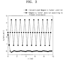
- FIG. 3 illustrates x-direction component s x of spin current of a magnetic tunnel junction according to a prior art and a magnetic tunnel junction according to an example embodiment of the present disclosure.
- a magnetic tunnel junction 101 includes a free magnetic body 120 having a structure in which a unit structure 120a including [auxiliary free magnetic layer 122a/free non-magnetic layer 124a] are repeated N times.
- FIG. 3 illustrates the x-direction component s x of the spin current calculated quantum-mechanically based on the non-equilibrium Green's function (NEGF) technique with respect to a thickness-direction axis (z-axis) of a free magnetic body.
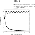
- FIG. 4 is a graph depicting a thickness average of the spin x-direction component in FIG. 3 .
- the ⁇ s x > is defined as below.
- the ⁇ s x > is in proportion to total spin-orbit spin torque that is actually felt by a free magnetic body having a thickness d .
- a ferromagnetic coherence length ⁇ c is very short. Therefore, the ⁇ s x > has a dependency of 1/ d . That is, when the thickness d of the free magnetic body increases, spin torque efficiency decreases by about 1/ d .
- Tight-binding Hamiltonian H was used for an existing magnetic tunnel junction structure of [spin polarization layer SP/non-magnetic body NM/free magnetic body (magnetic layer) FM] and a magnetic tunnel junction structure according to the present disclosure in which [spin polarization layer SP/non-magnetic body NM/free magnetic body([magnetic layer FM/non-magnetic layer NM])] is repeated.
- the tight-binding Hamiltonian H is given by Equations (5) to (7).
- H SP , H NM , and H FM represent Hamiltonians of layers, respectively; t represents a hopping constant, i and j represent site indexes, respectively; a ⁇ represents a creation operator; a represents an annihilation operator; ⁇ SP represents exchange interaction energy of a spin polarization layer; ⁇ represents a Pauli spin matrix; and m ⁇ represents a unit vector of polarization direction.
- ⁇ i represent JS of an i layer
- J represents a size of exchange interaction between an angular momentum S of magnetization and a non-equilibrium spin density S by current, and S represents
- G represents a Green's function
- E represents energy
- I represents a unit matrix
- G n represents a correlation function
- ⁇ represents an electron density
- ⁇ ⁇ represents a non-equilibrium electron density depending on application of a voltage.
- the magnetization of the spin polarization layer was set to the y direction.
- a magnetization direction in all sites of the free magnetic body was set to +z direction.
- a magnetization of an odd one of magnetic layers constituting a free magnetic body was set to +z direction and a magnetization of an even magnetic layer was set to -z direction.
- Equation (11) A dependency of critical current I c on a thickness of a free magnetic body at a magnetic tunnel junction according to the present disclosure was confirmed through micromagnetics.
- Equation (11) ⁇ represents a magnetic rotational constant
- H eff represents all effective magnetic field vectors of a free magnetic field 103 or 203
- ⁇ represents a Gilbert damping constant
- N SOT represents a spin-orbit spin torque
- FIG. 5 illustrates variation of critical current I c for magnetization reversal depending on a thickness d of a free magnetic body in an existing magnetic tunnel junction and a magnetic tunnel junction according to the present disclosure.
- FIG. 6 illustrates variation of a thermal stability factor ⁇ depending on a thickness d of a free magnetic body in a magnetic tunnel junction according to the present disclosure.
- a thermal stability factor ⁇ increases as a thickness d of a free magnetic body increases.
- critical current I c is constant irrespective of d. Accordingly, when the magnetic tunnel junction according to an example embodiment of the present disclosure is used as a smaller-sized memory or logic device cell, it is driven at low current while keeping non-volatility. This characteristic makes a low-power ultrahigh-density nonvolatile device possible.
- Equation (12) ⁇ represents a gyromagnetic constant and H eff represents all effective magnetic field vectors.
- E B was determined.
- FIG. 7 illustrates a magnetic tunnel junction device according to an example embodiment of the present disclosure.
- a magnetic tunnel junction device 200 includes a magnetic tunnel junction 201 including a fixed magnetic body 240, an insulator 130, and a free magnetic body 120 that are sequentially stacked and a conducting wire 110 disposed adjacent to the free magnetic body 120 of the magnetic tunnel junction 201 to apply in-plane current to the magnetic tunnel junction 201.
- the fixed magnetic body 240 has a fixed magnetization direction and is a thin film including a material magnetized in a direction perpendicular to a film surface.
- the free magnetic body 120 has a structure of [auxiliary free magnetic layers 122a to 122n/free non-magnetic layers 124a to 124n] N /main free magnetic layer 126, where N is a positive integer greater than or equal to 2 and indicates that an [auxiliary free magnetic layers 122a to 122n/free non-magnetic layers 124a to 124n] structure is stacked repeatedly N times.
- Each of the main free magnetic layer 126 and the auxiliary free magnetic layers 122a to 122n changes in magnetization direction and is a thin film magnetized in a direction perpendicular to a film surface.
- the main free magnetic body 120 is disposed adjacent to the conducting wire 110 that generates spin current due to the in-plane current.
- the free magnetic layers 122a to 122n and 126 constituting the free magnetic body 120 two magnetic layers closest to each other are magnetized in opposite directions by RKKY exchange interaction through the free magnetic layers 124a to 124n.
- the fixed magnetic body 240 may have a synthetic antiferromagnetic structure including a first fixed magnetic layer 244, a fixed non-magnetic layer 246, and a second fixed magnetic layer 248 that are sequentially stacked.
- Each of the first fixed magnetic layer 244 and the second fixed magnetic layer 248 may independently include at least one of Fe, Co, Ni, B, Si, Zr, and a combination thereof.
- the fixed non-magnetic layer 246 may include at least one of Ru, Ta, Cu, and a combination thereof.
- the fixed magnetic body 240 may be an exchange-biased antiferromagnetic structure including an antiferromagnetic layer 242, a first fixed magnetic layer 244, a fixed non-magnetic layer 246, and a second fixed magnetic layer 248 that are sequentially stacked.
- the antiferromagnetic layer 242 may be formed of a material including at least one of Ir, Pt, Mn, and a combination thereof.
- Each of the first and second fixed magnetic layers 244 and 248 may be independently formed of a material including at least one of Fe, Co, Ni, B, Si, Zr, and a combination thereof.
- the fixed non-magnetic layer 246 may be formed of a material including at least one of Ru, Ta, Cu, and a combination thereof.
- FIG. 8 illustrates a magnetic tunnel junction device according to another example embodiment of the present disclosure.
- a magnetic tunnel junction 300 includes a magnetic tunnel junction 301 including a fixed magnetic body 140, an insulator 130, and a free magnetic body 320 that are sequentially stacked and a conducting wire 110 disposed adjacent to the free magnetic body 320 of the magnetic tunnel junction 301 to apply in-plane current to the magnetic tunnel junction 301.
- the fixed magnetic body 140 has a fixed magnetization direction and is a thin film including a material magnetized in a direction perpendicular to a film surface.
- the free magnetic body 320 has a structure of [auxiliary free magnetic layers 322a to 322n/free non-magnetic layers 324a to 324n] N /main free magnetic layer 326, where N is a positive integer greater than or equal to 2 and indicates that an [auxiliary free magnetic layers 322a to 322n/free non-magnetic layers 324a to 324n] structure (320a to 320n) is stacked repeatedly N times.
- N is a positive integer greater than or equal to 2 and indicates that an [auxiliary free magnetic layers 322a to 322n/free non-magnetic layers 324a to 324n] structure (320a to 320n) is stacked repeatedly N times.
- Each of the main free magnetic layer 326 and the auxiliary free magnetic layers 322a to 322n changes in magnetization direction and is a thin film magnetized in a direction perpendicular to a film surface.
- the main free magnetic layer 326 is disposed adjacent to the conducting wire 110 that generates spin current due to the in-plane
- the fixed magnetic body 140 may not be aligned with the free magnetic body 320. Specifically, the fixed magnetic body 140 and the free magnetic body 320 may extend parallel to each other in an extending direction of the conducting wire 110.
- the free magnetic layer 320 may include at least one magnetic domain structure 321.
- each of the main free magnetic layer 326 and the auxiliary free magnetic layers 322a to 322n may include at least one magnetic domain structure 321.
- the magnetic domain structure 321 may move in an x axis direction due to in-plane current flowing to the conducting wire 110.
- the magnetic domain structure 321 may be a magnetic domain wall or a skyrmion and may divide a magnetic domain in opposite directions.
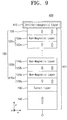
- FIG. 9 illustrates a magnetic tunnel junction device according to another example embodiment of the present disclosure.
- a magnetic tunnel junction 400 includes a magnetic tunnel junction 101 including a fixed magnetic body 140, an insulator 130, and a free magnetic body 120 that are sequentially stacked and a conducting wire 410 disposed adjacent to the free magnetic body 120 of the magnetic tunnel junction 101 to apply in-plane current to the magnetic tunnel junction 101.
- the fixed magnetic body 140 has a fixed magnetization direction and is a thin film including a material magnetized in a direction perpendicular to a film surface.
- the free magnetic body 120 has a structure of [auxiliary free magnetic layers 122a to 122n/free non-magnetic layers 124a to 124n] N /main free magnetic layer 126, where N is a positive integer greater than or equal to 2 and indicates that an [auxiliary free magnetic layers 122a to 122n/free non-magnetic layers 124a to 124n] structure (120a to 120n) is stacked repeatedly N times.
- Each of the main free magnetic layer 126 and the auxiliary free magnetic layers 122a to 122n changes in magnetization direction and is a thin film magnetized in a direction perpendicular to a film surface.
- the main free magnetic layer 126 is disposed adjacent to the conducting wire 410 that generates spin current due to the in-plane current.
- the free magnetic layers 122a to 122n and 126 constituting the free magnetic body 320 two magnetic layers closest to each other are magnetized in opposite directions by RKKY exchange interaction through the free magnetic layers 124a to 124n.
- the conductor 410 may include a conductive antiferromagnetic body. Specifically, the conducting wire 410 may apply in-plane current and include an antiferromagnetic layer. The conducting wire 410 may provide an in-plane exchange bias magnetic field to the main free magnetic layer 126. Specifically, the conducting wire 410 may be FeMn, PtMn or IrMn. The antiferromagnetic layer may provide an exchange bias magnetic field to the free magnetic body 120. Thus, the magnetic tunnel junction device may switch a magnetization direction of a free magnetic body having perpendicular magnetic anisotropy without using an external magnetic field.
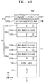
- FIG. 10 illustrates a magnetic tunnel junction device according to another example embodiment of the present disclosure.
- a magnetic tunnel junction device 500 includes a magnetic tunnel junction 101 including a fixed magnetic body 140, an insulator 130, and a free magnetic body 120 that are sequentially stacked and a conducting wire 510 disposed adjacent to the free magnetic body 120 of the magnetic tunnel junction 101 to apply in-plane current to the magnetic tunnel junction 101.
- the fixed magnetic body 140 has a fixed magnetization direction and is a thin film including a material magnetized in a direction perpendicular to a film surface.
- the free magnetic body 120 has a structure of [auxiliary free magnetic layers 122a to 122n/free non-magnetic layers 124a to 124n] N /main free magnetic layer 126, where N is a positive integer greater than or equal to 2 and indicates that an [auxiliary free magnetic layers 122a to 122n/free non-magnetic layers 124a to 124n] structure (120a to 120n) is stacked repeatedly N times.
- Each of the main free magnetic layer 126 and the auxiliary free magnetic layers 122a to 122n changes in magnetization direction and is a thin film magnetized in a direction perpendicular to a film surface.
- the main free magnetic layer 126 is disposed adjacent to the conducting wire 410 that generates spin current due to the in-plane current.
- two magnetic layers closest to each other are magnetized in opposite directions by RKKY exchange interaction through the free magnetic layers 124a to 124n:
- the conducting wire 510 applying the in-plane current may include an antiferromagnetic layer 510a and a ferromagnetic layer 510b that are sequentially stacked.
- the antiferromagnetic layer 510a may be disposed adjacent to the main free magnetic layer 126.
- the ferromagnetic layer 510b may have an in-plane magnetization direction or a magnetization direction in which the ferromagnetic layer 510b extends.
- the conducting wire 510 may provide an in-plane exchange bias magnetic field to the main free magnetic layer 126.
- the free magnetic body 120 may be switched without using an external magnetic field.
- the ferromagnetic layer 510b has in-plane magnetic anisotropy and provides a function to antiferromagnetically align the antiferromagnetic layer 510a in an in-plane direction.
- the antiferromagnetic layer 510a adjacent to the free magnetic body 120 having perpendicular magnetic anisotropy establishes an exchange bias magnetic field of a direction perpendicular to the free magnetic body 120 having the perpendicular magnetic anisotropy.
- the ferromagnetic layer 510b is antiferromagnetically aligned with the antiferromagnetic layer 510a in the in-plane direction by exchange interaction between the antiferromagnetic layer 510b having in-plane magnetic anisotropy and the antiferromagnetic layer 510a.
- an exchange bias magnetic field of a horizontal direction is induced to the free magnetic body 120 having perpendicular magnetic anisotropy adjacent to an opposite side by an antiferromagnetic rule.
- Current flowing to the conducting wire 510 including the antiferromagnetic layer 510a generates a spin-orbit spin torque through anomalous Hall effect or spin Hall effect.
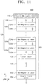
- FIG. 11 illustrates a magnetic tunnel junction device according to another example embodiment of the present disclosure.
- a magnetic tunnel junction device 600 includes a magnetic tunnel junction 601 including a fixed magnetic body 140, an insulator 130, and a free magnetic body 120 that are sequentially stacked and a conducting wire 110 disposed adjacent to the free magnetic body 120 of the magnetic tunnel junction 101 to apply in-plane current to the magnetic tunnel junction 101.
- the fixed magnetic body 140 has a fixed magnetization direction and is a thin film including a material magnetized in a direction perpendicular to a film surface.
- the free magnetic body 120 has a structure of [auxiliary free magnetic layers 122a to 122n/free non-magnetic layers 124a to 124n] N /main free magnetic layer 126, where N is a positive integer greater than or equal to 2 and indicates that an [auxiliary free magnetic layers 122a to 122n/free non-magnetic layers 124a to 124n] structure (120a to 120n) is stacked repeatedly N times.
- Each of the main free magnetic layer 126 and the auxiliary free magnetic layers 122a to 122n changes in magnetization direction and is a thin film magnetized in a direction perpendicular to a film surface.
- the main free magnetic layer 126 is disposed adjacent to the conducting wire 110 that generates spin current due to the in-plane current.
- two magnetic layers closest to each other are magnetized in opposite directions by RKKY exchange interaction through the free magnetic layers 124a to 124n.
- a dipole filed non-magnetic layer 652 and a dipole field ferromagnetic layer 654 having an in-plane magnetization direction are sequentially stacked adjacent to the fixed magnetic body 140.
- the dipole field non-magnetic layer 652 is disposed adjacent to the fixed magnetic body 140.
- the dipole field non-magnetic layer 652 may be a conductive metal layer including at least one of Ru, Ta, Cu, and a combination thereof.
- the dipole field ferromagnetic layer 654 may have an in-plane magnetization direction (e.g., -x axis direction) and may establish a dipole magnetic field a dipole magnetic field to establish a magnetic field at the free magnetic body 120 in an in-plane direction (+x axis direction).
- the free magnetic body 120 of the magnetic tunnel junction device 600 may perform magnetization reversal without using an external magnetic field.
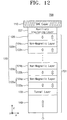
- FIG. 12 illustrates a magnetic tunnel junction device according to another example embodiment of the present disclosure.
- a magnetic tunnel junction device 700 includes a magnetic tunnel junction 701 including a fixed magnetic body 140, an insulator 130, and a free magnetic body 120 that are sequentially stacked and a conducting wire 110 disposed adjacent to the free magnetic body 120 of the magnetic tunnel junction 701 to apply in-plane current to the magnetic tunnel junction 701.
- the fixed magnetic body 140 has a fixed magnetization direction and is a thin film including a material magnetized in a direction perpendicular to a film surface.
- the free magnetic body 120 has a structure of [auxiliary free magnetic layers 122a to 122n/free non-magnetic layers 124a to 124n] N /main free magnetic layer 126, where N is a positive integer greater than or equal to 2 and indicates that an [auxiliary free magnetic layers 122a to 122n/free non-magnetic layers 124a to 124n] structure (120a to 120n) is stacked repeatedly N times.
- Each of the main free magnetic layer 126 and the auxiliary free magnetic layers 122a to 122n changes in magnetization direction and is a thin film magnetized in a direction perpendicular to a film surface.
- the main free magnetic layer 126 is disposed adjacent to the conducting wire 110 that generates spin current due to the in-plane current.
- two magnetic layers closest to each other are magnetized in opposite directions by RKKY exchange interaction through the free magnetic layers 124a to 124n.
- An auxiliary insulating layer 727 is disposed between the conducting wire 110 and the free magnetic body 120.
- the auxiliary insulating layer 727 may include at least one of AlO x , MgO, TaOx, ZrO x , and a combination thereof.
- the auxiliary insulating layer may prevent in-plane charge current flowing along the conducting wire 110 from directly flowing through the magnetic tunnel junction 701 and allows only sure spin current to pass therethrough.
- FIG. 13 illustrates a magnetic tunnel junction device according to another example embodiment of the present disclosure.
- a magnetic tunnel junction device 800 includes a magnetic tunnel junction 101 including a fixed magnetic body 140, an insulator 130, and a free magnetic body 120 that are sequentially stacked and a conducting wire 810 disposed adjacent to the free magnetic body 120 of the magnetic tunnel junction 101 to apply in-plane current to the magnetic tunnel junction 101.
- the fixed magnetic body 140 has a fixed magnetization direction and is a thin film including a material magnetized in a direction perpendicular to a film surface.
- the free magnetic body 120 has a structure of [auxiliary free magnetic layers 122a to 122n/free non-magnetic layers 124a to 124n] N /main free magnetic layer 126, where N is a positive integer greater than or equal to 2 and indicates that an [auxiliary free magnetic layers 122a to 122n/free non-magnetic layers 124a to 124n] structure (120a to 120n) is stacked repeatedly N times.
- Each of the main free magnetic layer 126 and the auxiliary free magnetic layers 122a to 122n changes in magnetization direction and is a thin film magnetized in a direction perpendicular to a film surface.
- the main free magnetic layer 126 is disposed adjacent to the conducting wire 810 that generates spin current due to the in-plane current.
- the free magnetic layers 122a to 122n and 126 constituting the free magnetic body 320 two magnetic layers closest to each other are magnetized in opposite directions by RKKY exchange interaction through the free magnetic layers 124a to 124n.
- the conducting wire 810 may include a conducting wire non-magnetic layer 810a and a conducting wire ferromagnetic layer 810b that are sequentially stacked.
- the conducting wire ferromagnetic layer 810b may include an in-plane magnetization direction component.
- the conducting wire non-magnetic layer 810a may be disposed adjacent to the free magnetic body 120.
- the conducting wire non-magnetic layer 810a may include one material selected from Cu, Ta, Pt, W, Bi, Ir, Mn, Ti, Cr, and a combination thereof.
- the conducting wire ferromagnetic layer 810b may include at least one of Fe, Co, Ni, B, Si, Zr, and a combination thereof.
- Spin current may be generated through anomalous Hall effect or anisotropic magnetoresistance effect of the conducting wire ferromagnetic layer 810b by the in-plane charge current flowing through the conducting wire ferromagnetic layer 810b [ T. Taniguchi, J. Grollier, M. D. Stiles, Physical Review Applied 3, 044001 (2015 )].
- the spin current may be generated by effect of interface spin-orbit coupling [ V. P. Amin, M. D. Stiles, Physical Review B 94, 104419 (2016 )].
- FIG. 14 illustrates a magnetic tunnel junction device according to another example embodiment of the present disclosure.
- a magnetic tunnel junction device 900 includes a magnetic tunnel junction 901 including a fixed magnetic body 140, an insulator 130, and a free magnetic body 120 that are sequentially stacked and a conducting wire 910 disposed adjacent to the free magnetic body 120 of the magnetic tunnel junction 101 to apply in-plane current to the magnetic tunnel junction 901.
- the fixed magnetic body 140 has a fixed magnetization direction and is a thin film including a material magnetized in a direction perpendicular to a film surface.
- the free magnetic body 120 has a structure of [auxiliary free magnetic layers 122a to 122n/free non-magnetic layers 124a to 124n] N /main free magnetic layer 126, where N is a positive integer greater than or equal to 2 and indicates that an [auxiliary free magnetic layers 122a to 122n/free non-magnetic layers 124a to 124n] structure (120a to 120n) is stacked repeatedly N times.
- Each of the main free magnetic layer 126 and the auxiliary free magnetic layers 122a to 122n changes in magnetization direction and is a thin film magnetized in a direction perpendicular to a film surface.
- the main free magnetic layer 126 is disposed adjacent to the conducting wire 910 that generates spin current due to the in-plane current.
- the free magnetic layers 122a to 122n and 126 constituting the free magnetic body 320 two magnetic layers closest to each other are magnetized in opposite directions by RKKY exchange interaction through the free magnetic layers 124a to 124n.
- the conducting wire 910 may include a conducting wire non-magnetic layer 910a and a conducting wire ferromagnetic layer 910b that are sequentially stacked.
- a non-magnetic layer 927 may be provided between the conductive ferromagnetic layer 910a and the free magnetic body 120.
- the conducting wire ferromagnetic layer 910a may be disposed adjacent to the free magnetic body 120.
- the non-magnetic layer 927 may be aligned with a side surface of the free magnetic body 120.
- the conducting wire non-magnetic layer 910b and the non-magnetic layer 927 may include one material selected from Cu, Ta, Pt, W, Bi, Ir, Mn, Ti, Cr, and a combination thereof.
- the conducting wire ferromagnetic layer 910a may include at least one of Fe, Co, Ni, B, Si, Zr, and a combination thereof.
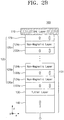
- FIG. 15 illustrates a magnetic memory device according to an example embodiment of the present disclosure.
- a magnetic memory device 91 includes a plurality of magnetic tunnel junctions 101.
- the magnetic tunnel junction 101 or a magnetic tunnel junction 100 may be variously modified as described with reference to FIGS. 2 to 14 .
- the magnetic memory device 91 includes a plurality of magnetic tunnel junctions 101 arranged on a substrate placement plane in a matrix format and a first conductive pattern 110 disposed adjacent to a free magnetic body 120 of the magnetic tunnel junction 101.
- a fixed magnetic body 140 has a fixed magnetization direction and is a thin film formed of a material magnetized in a direction perpendicular to a film surface.
- the free magnetic body 120 changes in a magnetization direction and is a thin film formed of a material magnetized in a direction perpendicular to a film surface.
- the free magnetic body 120 has a structure of [auxiliary free magnetic layer/free non-magnetic layer] N /main free magnetic layer, where N is a positive integer greater than or equal to 2 and indicates that an [auxiliary free magnetic layer/free non-magnetic layer] structure is stacked repeatedly N times.
- N is a positive integer greater than or equal to 2
- the magnetic tunnel junction 101 may include a fixed magnetic body, an insulator, and a free magnetic body that are sequentially stacked.
- the main free magnetic layer 126 may be disposed adjacent to the first conductive pattern 110, and the first conductive pattern 110 may generate spin current from in-plane current to switch a magnetization direction of the free magnetic body 120.
- the total thickness of the free magnetic body 120 is 2 nm or more to secure high thermal stability.
- N is a positive integer greater than or equal to 2
- adjacent auxiliary free magnetic layers may have magnetizations of opposite directions in the free magnetic body 120 by Ruderman-Kittel-Kasuya-Yosida (RKKY) exchange interaction.
- the entire thickness of the free magnetic body 120 may be 2 nm or more.
- the auxiliary free magnetic layer and the main free magnetic layer may be formed of different materials or may have different thicknesses, respectively.
- Each of the auxiliary free magnetic layer and the main free magnetic layer may have a thickness of about 0.3 nm.
- the first conductive pattern 110 may be formed of one material selected from Cu, Ta, Pt, W, Bi, Ir, Mn, Ti, Cr, and a combination thereof.
- the first conductive pattern 110 may provide spin current to the free magnetic layer and may apply a spin-orbit spin torque to the free magnetic body 120.
- the spin-orbit spin torque may contribute to magnetization reversal of the free magnetic body 120.
- the first conductive patterns 110 or BL may run parallel on a substrate plane in a first direction.
- a free magnetic body 120 of each of the magnetic tunnel junctions arranged in the first direction may be periodically arranged adjacent to the first conductive pattern 110.
- a second conductive pattern 182 or WL may be electrically connected to a fixed magnetic body 140 of each of the magnetic tunnel junctions 101 arranged in a second direction perpendicular to the first direction and may extend on the substrate plane in the second direction.
- the magnetic memory device 91 may operate as a cross-point memory.
- the magnetic memory device 91 may operate due to spin Hall effect generated by current flowing to the first conductive pattern 110 and critical current damping effect generated by a voltage applied to the second conductive pattern 182.
- the magnetic memory device 91 may operate due to spin Hall effect generated by current flowing to the first conductive pattern 110 and spin-transfer torque effect generated by current flowing through a selected magnetic tunnel junction.
- FIG. 16 illustrates a magnetic memory device according to another example embodiment of the present disclosure.
- a magnetic memory device 92 includes a plurality of magnetic tunnel junctions.
- the magnetic memory device 92 includes a plurality of magnetic tunnel junctions 101 arranged on a substrate placement plane in a matrix format and a first conductive pattern 110 disposed adjacent to a free magnetic body 120 of the magnetic tunnel junction 101.
- a fixed magnetic body 140 has a fixed magnetization direction and is a thin film formed of a material magnetized in a direction perpendicular to a film surface.
- the free magnetic body 120 changes in a magnetization direction and is a thin film formed of a material magnetized in a direction perpendicular to a film surface.
- the free magnetic body 120 has a structure of [auxiliary free magnetic layer/free non-magnetic layer] N /main free magnetic layer, where N is a positive integer greater than or equal to 2 and indicates that an [auxiliary free magnetic layer/free non-magnetic layer] structure is stacked repeatedly N times.
- N is a positive integer greater than or equal to 2
- the magnetic tunnel junction 101 may include a fixed magnetic body, an insulator, and a free magnetic body that are sequentially stacked.
- the first conductive pattern 110 may be periodically disposed to be spaced apart from a substrate plane in a first direction.
- a free magnetic body 120 of each of the magnetic tunnel junctions arranged in the first direction may be periodically disposed adjacent to the first conductive pattern 110.
- the first conductive pattern 110 may provide spin current to the free magnetic layer and may apply a spin-orbit spin torque to the free magnetic body 120.
- the spin-orbit spin torque may contribute to magnetization reversal of the free magnetic body 120.
- a second conductive pattern 282 or WL is electrically connected to a fixed magnetic body 140 of each of the magnetic tunnel junctions arranged in the first direction and extends on the substrate plane in the first direction.
- a third conductive pattern 283 or SL is connected to one end of each of the first conductive patterns 110 arranged in the first direction and extends in the first direction.
- a fourth conductive pattern 284 or BL is connected to the other end of each of the first conductive patterns 110 arranged in the second direction and extends in the second direction.
- the magnetic memory device 92 may operate as a modified cross-point memory.
- the first conductive pattern 110 may be divided to inject spin current to the free magnetic body 120.
- in-plane current flowing to the first conductive pattern 110 may contribute to magnetization reversal of the free magnetic body 120 by injecting the spin current into the free magnetic body 120.
- FIG. 17 illustrates a magnetic memory device according to another example embodiment of the present disclosure.
- a magnetic memory device 93 includes a plurality of magnetic tunnel junctions.
- the magnetic memory device 93 includes a plurality of magnetic tunnel junctions 101 arranged in a matrix format and a first conductive pattern 110 disposed adjacent to a free magnetic body 120 of the magnetic tunnel junction 101.
- a fixed magnetic body 140 has a fixed magnetization direction and is a thin film formed of a material magnetized in a direction perpendicular to a film surface.
- the free magnetic body 120 changes in a magnetization direction and is a thin film formed of a material magnetized in a direction perpendicular to a film surface.
- the free magnetic body 120 has a structure of [auxiliary free magnetic layer/free non-magnetic layer] N /main free magnetic layer, where N is a positive integer greater than or equal to 2 and indicates that an [auxiliary free magnetic layer/free non-magnetic layer] structure is stacked repeatedly N times.
- N is a positive integer greater than or equal to 2
- the magnetic tunnel junction 101 may include a fixed magnetic body, an insulator, and a free magnetic body that are sequentially stacked.
- the first conductive pattern 110 may extend on a substrate plane in a first direction, and a free magnetic body 120 of each of the magnetic tunnel junctions arranged in the first direction may be periodically disposed adjacent to the first conductive pattern 110 or BL.
- the first conductive pattern 110 may provide spin current to the free magnetic layer and may apply spin-orbit spin torque to the free magnetic body 120.
- the spin-orbit spin torque may contribute to magnetization reversal of the free magnetic body 120.
- Selection transistors TR may be electrically connected to fixed magnetic bodies 140 of the magnetic tunnel junctions 101, respectively.
- a second conductive pattern 382 or SL may be electrically connected to a source/drain of each of the selection transistors arranged in the first direction and may extend on the substrate plane in the first direction.
- a third conductive pattern 383 or WL may be connected to a gate of each of selection transistors arranged in a second direction perpendicular to the first direction.
- a specific first conductive pattern 110 When current flows to a specific first conductive pattern 110 (BL0), free magnetic layers of all magnetic tunnel junctions connected to the first conductive pattern 110 may receive spin current.
- a voltage is applied to a specific third conductive pattern connected to a gate of the selection transistor TR to select a specific memory cell. Accordingly, a specific memory cell may receive spin current generated by the first conductive pattern and may receive a voltage or spin-transfer current generated by a fixed magnetic layer due to the selected selection transistor. As a result, the specific memory cell may perform a write operation.
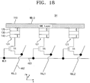
- FIG. 18 illustrates a magnetic memory device according to another example embodiment of the present disclosure.
- a magnetic memory device 94 includes a plurality of magnetic tunnel junctions.
- the magnetic memory device 94 includes a plurality of magnetic tunnel junctions 101 arranged in a matrix format and a first conductive pattern 110 disposed adjacent to a free magnetic body 120 of the magnetic tunnel junction 101.
- a fixed magnetic body 140 has a fixed magnetization direction and is a thin film formed of a material magnetized in a direction perpendicular to a film surface.
- the free magnetic body 120 changes in a magnetization direction and is a thin film formed of a material magnetized in a direction perpendicular to a film surface.
- the free magnetic body 120 has a structure of [auxiliary free magnetic layer/free non-magnetic layer] N /main free magnetic layer, where N is a positive integer greater than or equal to 2 and indicates that an [auxiliary free magnetic layer/free non-magnetic layer] structure is stacked repeatedly N times.
- N is a positive integer greater than or equal to 2
- the magnetic tunnel junction 101 may include a fixed magnetic body, an insulator, and a free magnetic body that are sequentially stacked.
- the first conductive pattern 110 or WBL may extend on a substrate plane in a first direction, and a free magnetic body 120 of each of the magnetic tunnel junctions arranged in the first direction may be periodically disposed adjacent to the first conductive pattern 110.
- the first conductive pattern 110 may provide spin current to the free magnetic layer and may apply a spin-orbit spin torque to the free magnetic body 120.
- the spin-orbit spin torque may contribute to magnetization reversal of the free magnetic body 120.
- Selection transistors TR may be electrically connected to fixed magnetic bodies 140 of the magnetic tunnel junctions 101, respectively.
- a second conductive pattern 482 or RBL may be electrically connected to a source/drain of each of selection transistors TR arranged in a second direction perpendicular to the first direction and may extend on the substrate plane in the second direction.
- a third conductive pattern 483 or WL may be connected to a gate of each of the selection transistor arranged in the first direction.
- a specific first conductive pattern is selected and current flows to the selected first conductive pattern.
- a third conductive pattern connected to a gate of a selection transistor connected to the selected memory cell is selected, so a voltage is applied to the fixed magnetic layer or spin-transfer current flows to the fixed magnetic layer.
- the specific memory cell may perform a write operation.
- FIG. 19 illustrates a magnetic memory device according to another example embodiment of the present disclosure.
- a magnetic memory device 95 includes a plurality of magnetic tunnel junctions.
- the magnetic memory device 95 includes a plurality of magnetic tunnel junctions 101 arranged in a matrix format and a first conductive pattern 110 disposed adjacent to a free magnetic body 120 of the magnetic tunnel junction 101.
- a fixed magnetic body 140 has a fixed magnetization direction and is a thin film formed of a material magnetized in a direction perpendicular to a film surface.
- the free magnetic body 120 changes in a magnetization direction and is a thin film formed of a material magnetized in a direction perpendicular to a film surface.
- the free magnetic body 120 has a structure of [auxiliary free magnetic layer/free non-magnetic layer] N /main free magnetic layer, where N is a positive integer greater than or equal to 2 and indicates that an [auxiliary free magnetic layer/free non-magnetic layer] structure is stacked repeatedly N times.
- N is a positive integer greater than or equal to 2
- the magnetic tunnel junction 101 may include a fixed magnetic body 140, an insulator 130, and a free magnetic body 120 that are sequentially stacked.
- the first conductive pattern 110 or WBL may extend on a substrate plane in a first direction, and a free magnetic body 120 of each of the magnetic tunnel junctions arranged in the first direction may be periodically disposed adjacent to the first conductive pattern 110.
- the first conductive pattern 110 may provide spin current to the free magnetic layer and may apply a spin-orbit spin torque to the free magnetic body 120.
- the spin-orbit spin torque may contribute to magnetization reversal of the free magnetic body 120.
- a second conductive pattern 582 or RBL may be electrically connected to a fixed magnetic body 140 of each of the magnetic tunnel junctions arranged in the first direction and may extend in the first direction.
- a third conductive pattern 583 or WBL may be connected to one end of each of the first conductive patterns 110 arranged in the first direction and may extend in the first direction.
- Selection transistors may be connected to the other ends of the first conductive patterns 110, respectively.
- a fourth conductive pattern 584 or SL may be connected to a source/drain of each of the selection transistors TR arranged in the first direction and may extend in the first direction.
- a fifth conductive pattern 585 or WL may be connected to a gate of each of selection transistors arranged in a second direction perpendicular to the first direction and may extend in the second direction.
- FIG. 20 illustrates a magnetic memory device according to another example embodiment of the present disclosure.
- a magnetic memory device 96 includes a plurality of magnetic tunnel junctions.
- the magnetic memory device 96 includes a plurality of magnetic tunnel junctions 101 arranged in a matrix format and a first conductive pattern 110 disposed adjacent to a free magnetic body 120 of the magnetic tunnel junction 101.
- a fixed magnetic body 140 has a fixed magnetization direction and is a thin film formed of a material magnetized in a direction perpendicular to a film surface.
- the free magnetic body 120 changes in a magnetization direction and is a thin film formed of a material magnetized in a direction perpendicular to a film surface.
- the free magnetic body 120 has a structure of [auxiliary free magnetic layer/free non-magnetic layer] N /main free magnetic layer, where N is a positive integer greater than or equal to 2 and indicates that an [auxiliary free magnetic layer/free non-magnetic layer] structure is stacked repeatedly N times.
- N is a positive integer greater than or equal to 2
- the magnetic tunnel junction 101 may include a fixed magnetic body 140, an insulator 130, and a free magnetic body 120 that are sequentially stacked.
- the first conductive pattern 110 or WBL may extend on a substrate plane in a first direction, and a free magnetic body 120 of each of the magnetic tunnel junctions arranged in the first direction may be periodically disposed adjacent to the first conductive pattern 110.
- the first conductive pattern 110 may provide spin current to the free magnetic layer and may apply a spin-orbit spin torque to the free magnetic body 120.
- the spin-orbit spin torque may contribute to magnetization reversal of the free magnetic body 120.
- Selection transistors TR may be connected to fixed magnetic body 140 of the magnetic tunnel junctions 101, respectively.
- a second conductive pattern 682 or RBL may be connected to a source/drain of each of the selection transistors TR arranged in the first direction and may extend in the first direction.
- a third conductive pattern 683 or WL may be connected to a gate of each of selection transistors TR arranged in a second direction perpendicular to the first direction and may extend in the second direction.
- a fourth conductive pattern 684 or WBL may be connected to one end of each of the first conductive pattern 110 arranged in the first direction and may extend in the first direction.
- a fourth conductive pattern 685 or SL may be connected to the other end of the first conductive pattern 110 arranged in the first direction and may extend in the first direction.
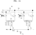
- FIG. 21 illustrates a magnetic memory device according to another example embodiment of the present disclosure.
- a magnetic memory device 97 includes a plurality of magnetic tunnel junctions.
- the magnetic memory device 97 includes a plurality of magnetic tunnel junctions 101 arranged in a matrix format and a first conductive pattern 110 disposed adjacent to a free magnetic body 120 of the magnetic tunnel junction 101.
- a fixed magnetic body 140 has a fixed magnetization direction and is a thin film formed of a material magnetized in a direction perpendicular to a film surface.
- the free magnetic body 120 changes in a magnetization direction and is a thin film formed of a material magnetized in a direction perpendicular to a film surface.
- the free magnetic body 120 has a structure of [auxiliary free magnetic layer/free non-magnetic layer] N /main free magnetic layer, where N is a positive integer greater than or equal to 2 and indicates that an [auxiliary free magnetic layer/free non-magnetic layer] structure is stacked repeatedly N times.
- N is a positive integer greater than or equal to 2
- the magnetic tunnel junction 101 may include a fixed magnetic body 140, an insulator 130, and a free magnetic body 120 that are sequentially stacked.
- the first conductive pattern 110 or WBL may extend on a substrate plane in a first direction, and a free magnetic body 120 of each of the magnetic tunnel junctions arranged in the first direction may be periodically disposed adjacent to the first conductive pattern 110.
- the first conductive pattern 110 may provide spin current to the free magnetic layer and may apply a spin-orbit spin torque to the free magnetic body 120.
- the spin-orbit spin torque may contribute to magnetization reversal of the free magnetic body 120.
- a second conductive pattern 782 may be electrically connected to each of fixed magnetic bodies 140 of the magnetic tunnel junctions 101 arranged in the first direction and may extend in the second direction.
- a first selection transistor TR1 may be connected to one end of each of the first conductive patterns 110.
- a second selection transistor TR2 may be connected to the other end of each of the first conductive patterns 110.
- a third conductive pattern 783 or WBL may be connected to a source/drain of the first selection transistor TR1 disposed in the first direction and may extend in the first direction.
- a fourth conductive pattern 784 or SL may be connected to a source/drain of the second transistor TR2 disposed in the first direction and may extend in the first direction.
- a fifth conductive pattern 785 may extend in the second direction by connecting a gate of the first selection transistor TR1 disposed in a second direction perpendicular to the first direction and a gate of the second selection transistor TR2 to each other.
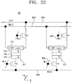
- FIG. 22 illustrates a magnetic memory device according to another example embodiment of the present disclosure.
- a magnetic memory device 98 includes a plurality of magnetic tunnel junctions.
- the magnetic memory device 98 includes a plurality of magnetic tunnel junctions 101 arranged in a matrix format and a first conductive pattern 110 disposed adjacent to a free magnetic body 120 of the magnetic tunnel junction 101.
- a fixed magnetic body 140 has a fixed magnetization direction and is a thin film formed of a material magnetized in a direction perpendicular to a film surface.
- the free magnetic body 120 changes in a magnetization direction and is a thin film formed of a material magnetized in a direction perpendicular to a film surface.
- the free magnetic body 120 has a structure of [auxiliary free magnetic layer/free non-magnetic layer] N /main free magnetic layer, where N is a positive integer greater than or equal to 2 and indicates that an [auxiliary free magnetic layer/free non-magnetic layer] structure is stacked repeatedly N times.
- N is a positive integer greater than or equal to 2
- the magnetic tunnel junction 101 may include a fixed magnetic body 140, an insulator 130, and a free magnetic body 120 that are sequentially stacked.
- the first conductive pattern 110 or WBL may extend on a substrate plane in a first direction, and a free magnetic body 120 of each of the magnetic tunnel junctions arranged in the first direction may be periodically disposed adjacent to the first conductive pattern 110.
- the first conductive pattern 110 may provide spin current to the free magnetic layer and may apply a spin-orbit spin torque to the free magnetic body 120.
- the spin-orbit spin torque may contribute to magnetization reversal of the free magnetic body 120.
- a first selection transistor TR1 may be connected to each of fixed magnetic bodies 140 of the magnetic tunnel junctions 101.
- a second selection transistor TR2 may be connected to one end of each of the first conductive patterns 110.
- a second conductive pattern 882 or RBL may be connected to a source/drain of the first selection transistor TR1 disposed in the first direction and may extend in the first direction.
- a third conductive pattern 883 or WBL may connect the other ends of the first conductive patterns 110 arranged in the first direction to each other and extend in the first direction.
- a fourth conductive pattern 884 or SL may connect sources/drains of the second selection transistors TR2 arranged in the first direction to each other and may extend in the first direction.
- a fifth conductive pattern 885 or WL may connect gates of first selection transistors arranged in a second direction perpendicular to the first direction to each other and may extend in the second direction.
- a sixth conductive pattern 886 or WL may connect gates of the second selection transistors arranged in the second direction to each other and may extend in the second direction.
- the free magnetic body 120 may include at least one magnetic domain structure.
- the magnetic domain structure may be a magnetic domain wall or a skyrmion.
- the first conductive pattern 110 may apply in-plane current and include an antiferromagnetic layer.
- the first conductive pattern 110 may provide an in-plane exchange bias magnetic field to the main free magnetic layer.
- the first conductive pattern 110 may apply in-plane current and include an antiferromagnetic layer and a ferromagnetic layer that are sequentially stacked.
- the antiferromagnetic layer is disposed adjacent to the main free magnetic layer, the ferromagnetic layer has an in-plane magnetization direction, the first conductive pattern provides an in-plane exchange bias magnetic field to the main free magnetic layer, and the free magnetic body may be switched without an external magnetic field.
- a dipole field non-magnetic layer and a dipole field ferromagnetic layer having an in-plane magnetization direction, which are sequentially stacked adjacent to the fixed magnetic body, may be further provided.
- the non-magnetic layer may be disposed adjacent to the fixed magnetic body.
- the free magnetic body may be switched without an external magnetic field by an in-plane magnetic field provided from the dipole field ferromagnetic layer.
- an auxiliary insulating layer may be further provided between the first conductive pattern 110 and the free magnetic body 120.
- the first conductive pattern 110 may include a first conductive pattern non-magnetic layer and a first conductive pattern magnetic layer that are sequentially stacked, and the first conductive pattern magnetic layer may include an in-plane magnetization direction component.
- the first conductive pattern 110 may include a first conductive pattern magnetic layer and a first conductive pattern non-magnetic layer that are sequentially stacked and may include a non-magnetic layer disposed between the first conductive pattern magnetic layer and the free magnetic body.
- a magnetic tunnel junction device may provide a characteristic in which efficiency of a spin-orbit spin torque is not in proportion to a thickness of a free magnetic body and is relatively irrelevant thereto, by using a characteristic in which when current flows along a conducting wire adjacent to the free magnetic body in an in-plane direction, spin current generated by spin Hall effect or Rashba effect is not entirely absorbed to a surface of the free magnetic body and is relatively uniformly absorbed throughout the thickness of the free magnetic body.
- the total thickness d of the free magnetic body increases by increasing N of a structure of [magnetic layer/non-magnetic layer] N /magnetic layer, thermal stability is improved while critical current I c is irrelevant to the total thickness d of the free magnetic body.
- non-volatility may be secured (e.g., ⁇ > 50) and a device may be driven through low critical current even when a magnetic tunnel junction having a very small cross-sectional area is used.
- a magnetic tunnel junction structure may be implemented to enable an ultrahigh nonvolatile device to be driven at low power.
Landscapes
- Engineering & Computer Science (AREA)
- Computer Hardware Design (AREA)
- Manufacturing & Machinery (AREA)
- Mram Or Spin Memory Techniques (AREA)
- Hall/Mr Elements (AREA)
- Thin Magnetic Films (AREA)
Abstract
Description
- The present disclosure relates to a magnetic tunnel junction that may be variously used in a magnetic memory device, a magnetic logic device, a magnetic sensor or the like, and more particularly to a spin-orbit torque magnetic tunnel junction that applies in-plane current to a conducting wire to generate a spin-orbit spin torque by spin Hall effect or Rashba effect.
- A ferromagnetic body means a material that is spontaneously magnetized even though a strong magnetic field is not applied thereto from the outside. In a magnetic tunnel junction structure (first magnetic body/insulator/second magnetic body) in which an insulator is interposed between two ferromagnetic bodies, an electric resistance varies depending on relative magnetization directions of two magnetic layers, i.e., a tunnel magnetoresistance effect occurs. The tunnel magnetoresistance effect occurs because up-spin and down-spin electrons flow at different degrees at the magnetic tunnel junction structure while tunneling an insulator.
- According to the law of action and reaction that is Newton's third law of motion, if the magnetization direction may control a flow of current, it is also possible to control a magnetization direction of the magnetic layer by applying current due to the reaction. If current is applied to the magnetic tunnel junction structure in a direction perpendicular to a film surface, the current spin-polarized by a first magnetic body (fixed magnetic layer) transfers its spin angular momentum while passing through a second magnetic body (free magnetic layer). A torque felt by magnetization due to the transfer of spin angular momentum is called a spin transfer torque. It is possible to fabricate a device for reversing the free magnetic layer or continuously rotating the free magnetic layer using the spin transfer torque or a device for moving a magnetic domain wall of the free magnetic layer using the spin transfer torque.
- Moreover, the magnetic tunnel junction may lead to magnetization reversal of a free magnetic layer or movement of a magnetic domain by using a spin-orbit spin torque generated by in-plane current flowing in a conducting wire adjacent to the free magnetic layer.
- A magnetization reversal device using a spin-orbit spin torque is disclosed in
U.S. Patent No. 8,416,618 B2 . -
FIG. 1 is a cross-sectional view illustrating a structure of a magnetic tunnel junction using a spin-orbit spin torque according to a prior art. - Referring to
FIG. 1 , a magnetictunnel junction device 10 includes a spinHall material layer 11 and a magnetic tunnel junction connected to the spinHall material layer 11. The magnetic tunnel junction includes a fixedmagnetic layer 14, atunnel insulating layer 13, and a freemagnetic layer 12 which are sequentially stacked. The freemagnetic layer 12 receives spin current from the spinHall material layer 11 to perform magnetization reversal. - Embodiments of the present disclosure provide a magnetic tunnel junction including a free magnetic body of a new structure to overcome a disadvantage in which low critical current and high thermal stability cannot be simultaneously obtained due to the problem that both critical current Ic and a thermal stability factor Δ are in proportion to a thickness d of a free magnetic body in a magnetic tunnel junction structure reversing or handling a magnetization direction using a spin-orbit spin torque according to a prior art.
- Embodiments of the present disclosure provide a magnetic tunnel junction using a spin-orbit spin torque that operates without an external magnetic field.
- Embodiments of the present disclosure provide a magnetic memory device using a spin-orbit spin torque.
- A magnetic tunnel junction device according to an example embodiment of the present disclosure includes a magnetic tunnel junction including a fixed magnetic body, an insulator, and a free magnetic body which are sequentially stacked and a conducting wire disposed adjacent to the free magnetic body of the magnetic tunnel junction to apply in-plane current to the magnetic tunnel junction. In the magnetic tunnel junction device, the fixed magnetic body may have a fixed magnetization direction and may be a thin film including a material magnetized in a direction perpendicular to a film surface. The free magnetic body may have a structure of [auxiliary free magnetic layer/free non-magnetic layer]N/main free magnetic layer, where N is a positive integer greater than or equal to 2 and indicates that an [auxiliary free magnetic layers/free non-magnetic layers] structure is stacked repeatedly N times. Each of the main free magnetic layer and the auxiliary free magnetic layer may change in magnetization direction and may be a thin film including a material magnetized in a direction perpendicular to a film surface, and the main free magnetic layer may be disposed adjacent to a conducting wire generating spin current by the in-plane current.
- The present disclosure will become more apparent in view of the attached drawings and accompanying detailed description. The embodiments depicted therein are provided by way of example, not by way of limitation, wherein like reference numerals refer to the same or similar elements. The drawings are not necessarily to scale, emphasis instead being placed upon illustrating aspects of the present disclosure.
-
FIG. 1 is a cross-sectional view illustrating a structure of a magnetic tunnel junction using a spin-orbit spin torque according to a prior art. -
FIGS. 2A and2B are conceptual diagrams illustrating magnetization directions of a magnetic tunnel junction and a free magnetic layer according to an example embodiment of the present disclosure. -
FIG. 3 illustrates x-direction component Sx of spin current of a magnetic tunnel junction according to a prior art and a magnetic tunnel junction according to an example embodiment of the present disclosure. -
FIG. 4 is a graph depicting a thickness average of the spin x-direction component inFIG. 3 . -
FIG. 5 illustrates variation of critical current Ic for magnetization reversal depending on a thickness d of a free magnetic body in an existing magnetic tunnel junction and a magnetic tunnel junction according to the present disclosure. -
FIG. 6 illustrates variation of a thermal stability factor Δ depending on a thickness d of a free magnetic body in a magnetic tunnel junction according to the present disclosure. -
FIGS. 7 to 14 illustrate magnetic tunnel junction devices according to example embodiments of the present disclosure. -
FIGS. 15 to 22 illustrate a driving method and a disposition of a magnetic memory device according to example embodiments of the present disclosure. - According to an example embodiment of the present disclosure, a spin-orbit spin torque is generated by spin Hall effect or Rashba effect by applying in-plane current to a conducting wire adjacent to a free magnetic body magnetized in a direction perpendicular to a film surface. The spin-orbit spin torque reverses magnetization of the free magnetic body or moves a magnetic domain of a magnetic domain wall or the like in a magnetic tunnel junction. The free magnetic body has a structure of [magnetic layer/non-magnetic layer]N/magnetic layer. The [magnetic layer/non-magnetic layer]N means that a [magnetic layer/non-magnetic layer] structure is repeatedly stacked N times. In the whole free magnetic body structure, two arbitrary magnetic layers closest to each other have magnetizations of opposite directions by Ruderman-Kittel-Kasuya-Yosida (RKKY) exchange interaction. A magnetic layer disposed at one end of the structure of [magnetic layer/non-magnetic layer]N is disposed adjacent to a conducting wire generating spin current, and a magnetic layer disposed at the other end thereof is disposed adjacent to an insulator.
- A magnetic tunnel junction according to the present disclosure leads to magnetization reversal of a free magnetic body or movement of a magnetic domain structure by using a spin-orbit spin torque generated by in-plane current flowing in a conducting wire adjacent to the free magnetic body. Charge current flowing to the conducting wire in an in-plane direction is converted into spin current by spin-orbit coupling of the conducting wire. The spin current applies the spin-orbit spin torque to a free magnetic body adjacent to the conducting wire. As a result, it is possible to provide a device for reversing the free magnetic body or continuously rotating the free magnetic body or a device for moving a magnetic domain structure of the free magnetic body.
- With respect to a free magnetic body having perpendicular magnetic anisotropy, critical current Ic required for magnetization reversal of a free magnetic body by a spin-orbit spin torque generated by in-plane current flowing in the conducting wire is given by Equation (1) below [K.-S. Lee, S.-W. Lee, B.-C. Min, K.-J. Lee, Applied Physics Letters 102, 112410 (2013)].

- In the Equation (1), ℏ(=1.05×10⁻³⁴ J.s) represents a value obtained by dividing a Planck constant by 2π, e(=1.6×10⁻¹⁹ C) represents charge amount of electron, θSH represents an effective spin Hall angle determined by a conductive wire material and the free magnetic body, MS represents the saturated magnetization amount of a magnetic body, d represents a thickness of the free magnetic body, A represents an area to which the in-plane current flows, HK,eff represents a perpendicular magnetic anisotropy field of the free magnetic body, and Hx represents a magnetic field of an in-plane direction (coplanar with flow of current) which is applied to the free magnetic body.
- If a size of a memory unit cell is reduced for a high-density device, a magnetization direction fluctuates randomly by thermal energy at room temperature, which is called superparamagnetic limit. The superparamagnetic limit causes written magnetic information to be erased unwantedly. Time τ for which a magnetization direction is averagely maintained against the thermal energy is given by Equation (2) below.

- In the Equation (2), τ0 represents a reciprocal of an attempt frequency and is approximately 1 ns, Keff represents an effective perpendicular magnetic anisotropy energy density (Keff = HK,effMS /2), V represents the volume of a free magnetic body, AF represents a cross-sectional area of the free magnetic body, kB represents a Boltzmann constant (=1.381×10⁻¹⁶ erg/K), and T represents a Kelvin temperature, where KeffV/kBT is defined as a thermal stability factor Δ of a magnetic memory device. To be commercialized as a nonvolatile memory device, in general, the magnetic memory device should satisfy the condition of Δ > 50 at room temperature.
- From the Equations (1) and (2), it can be understood that both the critical current Ic of the magnetic tunnel junction and the thermal stability factor Δ increase as the thickness d of the free magnetic body increases. That is, if the free magnetic body is made thick to secure high thermal stability, more current is required for magnetization reversal. As a result, power consumption for driving a device increases. As discussed above, a magnetic tunnel junction and a magnetic memory device according to a prior art encounter the problem that both the critical current Ic and the thermal stability factor Δ are in proportion to the thickness d of the free magnetic body. Accordingly, it is difficult to implement a device which satisfies both lower power driving obtained by decreasing the critical current Ic and improved thermal stability obtained by increasing the thickness d of the free magnetic body.
- A purpose of the present invention is to provide a magnetic tunnel junction including a free magnetic body to overcome a disadvantage in which low critical current and high thermal stability cannot be simultaneously obtained due to the problem that both critical current Ic and a thermal stability factor Δ are in proportion to a thickness d of a free magnetic body in a magnetic tunnel junction structure reversing or handling a magnetization direction using a spin-orbit spin torque according to a prior art.
- In a magnetic tunnel junction structure according to a prior art, critical current Ic is in proportion to a thickness d of a free magnetic body. This is because spin current generating a spin-orbit spin torque is entirely absorbed at a surface of the free magnetic body. This characteristic of the spin torque is called "surface-torque characteristic". The surface-torque characteristic may be described by a spatial precession of a quantum-mechanical spin in the free magnetic body [M. D. Stiles and A. Zangwill, Physical Review B 66, 014407 (2002)]. In-plane current flowing to a conducting wire adjacent to the free magnetic body generates spin current flowing in a perpendicular direction by spin Hall effect or Rashba effect. The spin current impinges on the free magnetic body. Since up-spin and down-spin Fermi wave vectors of a magnetic body are different from each other, when a spin having a direction different from a magnetic moment direction of the free magnetic body impinges on the free magnetic body, the spin travels spatially while rapidly precessing around the magnetic moment. At this point, a spatial wavelength of the spin precession varies depending on a direction of incident electrons. Even when current flows in a solid in a specific direction in average, a direction of each of electrons constituting the current has all directions on Fermi surface of an electron band. Since spins traveling in another direction perform a precession while having different wavelengths, a spatially very fast phase difference occurs (dephasing). Considering all the above, a spin component having a different direction than the magnetic moment exists only within a fixed distance from a surface of the free magnetic body. Over the fixed distance, the spin component has the same direction as the magnetic moment. This distance is called a ferromagnetic coherence length λc and is given by Equation (3) below [A. A. Kovalev, G. E. W. Bauer, A. Brataas, Physical Review B 73, 054407 (2006)].

- In the Equation (3),


- The greater a size of exchange interaction of the free magnetic body (i.e., a difference between up-spin energy and down-spin energy), the greater

m and a spin direction of the spin current in the free magnetic body is referred to ass , the spin torque is in proportion to
s includes an


s of the spin current in the ferromagnetic body is different from the magnetic moment directionm only at a distance within λc from the surface of the free magnetic body. Therefore, a spin-orbit spin torque in the free magnetic body including the ferromagnetic body has a non-zero value only on the surface of the free magnetic body and thus is a surface torque applied only to the surface of the free magnetic body. Due to the surface torque characteristic, a size of the spin-orbit spin torque is not changed even when the thickness d of the free magnetic body increases. Instead, since the volume of the magnetic body whose magnetization direction should be moved by the spin torque increases, the critical current Ic is in proportion to the thickness d of the free magnetic body. - To overcome the problem that the critical current Ic is in proportion to the thickness d of the free magnetic body, there is proposed a structure in which a free magnetic body includes a plurality of magnetic layers and a magnetic moment of each of the magnetic layers is repeatedly reversed in a current flow direction. More specifically, a proposed free magnetic body has a structure in which [magnetic layer/non-magnetic layer] is repeated and magnetization directions of closest two magnetic layers are opposite to each other due to an RKKY exchange interaction through a non-magnetic layer. Due to the structure in which magnetizations of opposite directions are repeated arranged, an effective energy difference of up-spin and down-spin in the free magnetic layer is reduced. The reduction in the effective energy difference causes effective


- A simulation was performed to confirm that a bulk-torque characteristic was exhibited in a proposed novel free magnetic body structure.
- A magnetic tunnel junction according to example embodiments of the present disclosure uses a characteristic in which, when current flows in an in-plane direction along a conducting wire adjacent to a free magnetic body, spin current generated by spin Hall effect or Rashba effect is not entirely absorbed to a surface of the free magnetic layer but is relatively uniformly absorbed at the total thickness of the free magnetic body. Thus, efficiency of the spin-orbit torque is not in inverse proportion to a thickness of the free magnetic body and is relatively irrelevant to the thickness of the free magnetic body. To this end, the free magnetic body has a structure of [magnetic layer/non-magnetic layer]N/magnetic layer, where N is the repeated number of a [magnetic layer/non-magnetic layer] unit structure. If the total thickness of the free magnetic body increases by increasing N, the total magnetic volume increases to improve thermal stability. Thus, both high thermal stability and low critical current may be secured. As a result, although a magnetic tunnel junction having a very small cross-sectional area is used, the total thickness of the free magnetic body may increase to secure non-volatility (e.g., thermal stability factor Δ > 50) and to secure low critical current using a characteristic in which a spin torque is uniformly absorbed at the whole of thickness. Accordingly, an ultrahigh-density nonvolatile device with low power driving and high thermal stability may be implemented.
- Example embodiments will now be described more fully with reference to the accompanying drawings, in which some example embodiments are shown. Example embodiments may, however, be embodied in many different forms and should not be construed as being limited to the embodiments set forth herein; rather, these example embodiments are provided so that this disclosure will be thorough and complete, and will fully convey the scope of example embodiments of inventive concepts to those of ordinary skill in the art. In the drawings, the thicknesses of layers and regions are exaggerated for clarity. Like reference characters and/or numerals in the drawings denote like elements, and thus their description may be omitted.
-
FIGS. 2A and2B are conceptual diagrams illustrating magnetization directions of a magnetic tunnel junction and a free magnetic layer according to an example embodiment of the present disclosure. - Referring to
FIGS. 2A and2B , amagnetic tunnel device 100 includes amagnetic tunnel junction 101 including a fixedmagnetic body 140, aninsulator 130, and a freemagnetic body 120 which are sequentially stacked and aconducting wire 110 disposed adjacent to the freemagnetic body 120 of themagnetic tunnel junction 101 to apply in-plane current to themagnetic tunnel junction 101. - A magnetic field established from the outside of the free
magnetic body 120 may be applied to the freemagnetic body 120 or a structure of themagnetic tunnel device 100 may be changed to replace the external magnetic field. - The fixed
magnetic body 140 is a thin film that has a fixed magnetization direction and is magnetized in a direction perpendicular to a film surface. The freemagnetic body 120 has a structure of [auxiliary freemagnetic layers 122a to 122n/freenon-magnetic layers 124a to 124n]N/main freemagnetic layer 126, where N is a positive integer greater than or equal to 2 and indicates that an [auxiliary freemagnetic layers 122a to 122n/freenon-magnetic layers 124a to 124n] structure (120a to 120n) is stacked repeatedly N times. Each of the main freemagnetic layer 126 and the auxiliary freemagnetic layers 122a to 122n is a thin film that changes in magnetization direction and is magnetized in a direction perpendicular to a film surface. The main freemagnetic layer 126 is disposed adjacent to theconducting wire 110 that generates spin current due to the in-plane current. - The
conducting wire 110 manifests a spin-orbit spin torque due to spin Hall effect or Rashba effect by the in-plane current flowing in an in-plane direction. The spin-orbit spin torque reverses a magnetization of the freemagnetic body 120 or moves a magnetic domain structure. Theconducting wire 110 may be a single layer or a multi-layered structure including different materials. Theconducting wire 110 may include at least one of Cu, Ta, Pt, W, Bi, Ir, Mn, Ti, Cr, and a combination thereof. Theconducting wire 110 may be a heavy metal such as β-Ta, Pt, β-W, Pd or Cr. Theconducting wire 110 may be doped with an impurity such as oxygen. - The
magnetic tunnel junction 101 may include the fixedmagnetic body 140, theinsulator 130, and the freemagnetic body 120 that are sequentially stacked. Themagnetic tunnel junction 101 may be variously changed so long as it includes a free magnetic body. - The
insulator 130 may include a tunnel insulating layer. Theinsulator 130 may be a thin film formed of a material including at least one of AlOx, MgO, TaOx, ZrOx, and a combination thereof. - The fixed
magnetic body 140 may include a ferromagnetic material and may include at least one of Fe, Co, Ni, B, Si, Zr, and a combination thereof. More specifically, the fixedmagnetic body 140 may be Co, CoFe, CoFeB, CoNi or NiFe. - The fixed
magnetic body 140 may have a synthetic antiferromagnetic structure including a first fixed magnetic layer, a fixed non-magnetic layer, and a second fixed magnetic layer that are sequentially stacked. Each of the first and second fixed magnetic layers may independently include at least one of Fe, Co, Ni, B, Si, Zr, and a combination thereof, and the fixed non-magnetic layer may include at least one of Ru, Ta, Cu, and a combination thereof. - The fixed
magnetic body 140 may be an exchange-biased antiferromagnetic structure including an antiferromagnetic layer, a first fixed magnetic layer, a fixed non-magnetic layer, and a second fixed magnetic layer that are sequentially stacked. The antiferromagnetic layer may be formed of a material including at least one of Ir, Pt, Mn, and a combination thereof. Each of the first and second fixed magnetic layers may include a ferromagnetic material and may be independently formed of a material including Fe, Co, Ni, B, Si, Zr, and a combination thereof. The fixed non-magnetic layer may be formed of a material including at least one of Ru, Ta, Cu, and a combination thereof. - The free
magnetic body 120 has a structure in which aunit structure 120a including [auxiliary freemagnetic layer 122a/freenon-magnetic layer 124a] is repeated N times, and two auxiliary free magnetic layers closest to each other (e.g., 122a and 122b) have magnetic moments (magnetizations) of opposite directions by Ruderman-Kittel-Kasuya-Yosida (RKKY) exchange interaction through the freenon-magnetic layer 124a. Due to the same reason, the magnetization direction of the main freemagnetic layer 126 is opposite to that of the closest auxiliary freemagnetic layer 122n. - The auxiliary free
magnetic layers 122a to 122n all have perpendicular magnetic anisotropy and a magnetization direction perpendicular to a plane, and adjacent auxiliary magnetic layers have opposite magnetization directions. In addition, the main freemagnetic layer 126 and an auxiliary freemagnetic layer 122n closest to the main freemagnetic layer 126 have different magnetization directions. Magnetizations of the auxiliary freemagnetic layer 122a to 122n and the main freemagnetic layer 126 may be simultaneously reversed by the spin current. - The free
magnetic body 120 may have a structure in which [auxiliary freemagnetic layers 122a to 122n/freenon-magnetic layers 124a to 122n] is repeatedly stacked two or more times. - The auxiliary free
magnetic layers 122a to 122n and the main freemagnetic layer 126 may be formed of different materials or have different thicknesses, respectively. For example, the auxiliary freemagnetic layer 122a adjacent to thetunnel insulating layer 130 determines a tunnel magnetic resistance of themagnetic tunnel junction 101. The tunnel magnetic resistance determines a size of a regenerative signal of a magnetic device including themagnetic tunnel junction 101. Therefore, the higher the tunnel magnetic resistance, the more advantageous device driving. As a result, a material and a thickness of the auxiliary freemagnetic layer 122a may be different from those of the other auxiliary freemagnetic layers 122b to 122n and 126 to have a high tunnel magnetic resistance. In addition, the main freemagnetic layer 126 adjacent to theconducting wire 110 may have an influence on the intensity of spin current impinging on the freemagnetic body 120 by interface effect. Thus, the material and the thickness of the main freemagnetic layer 126 may be different from those of the auxiliary freemagnetic layers 122a to 122n to secure a large spin torque. In addition, magnetization reversal or magnetic domain driving efficiency may be improved by differentiating materials or thicknesses of two magnetic layers closest to each other (e.g., (122a and 122b) or (122c and 122d) or (122n and 126)). - Specifically, the auxiliary free
magnetic layer 122a adjacent to thetunnel insulating layer 130 may include CoFeB, and other magnetic layers in the other freemagnetic body 120 may include CoFe, Co or the like. Alternatively, the thickness of the auxiliary freemagnetic layer 122a adjacent to thetunnel insulating layer 130 may be greater than 1 nm to secure a high tunnel magnetic resistance. Alternatively, other magnetic layers in the freemagnetic body 120 except for the auxiliary freemagnetic layer 122a may be less than 1 nm, which is smaller than a ferromagnetic coherence length λc , to manifest a bulk-torque characteristic. - Electrons of up-spin and down-spin constituting in-plane charge current flowing in an x axis direction in the
conducting wire 110 are deflected in a different direction (e.g., y axis direction) by spin-orbit interaction. Spin currents are generated in all directions perpendicular to the in-plane charge current direction. In this case, the spin current generated in all the directions have spin components deflected in directions perpendicular to all the directions. - When the in-plane current in the
conducting wire 110 flows in the x axis direction, among the generated spin currents, -z axis component (spin current impinging on a free magnetic body) has a spin components of y direction or -y direction according to types of materials of theconducting wire 110 and the adjacent main freemagnetic layer 126 and flows into the freemagnetic body 120. Due to the spin current flowing into the freemagnetic body 120, the freemagnetic body 120 receives a spin-orbit spin torque. - A direction of the spin-orbit spin torque made by the spin current impinging on the free
magnetic body 120 is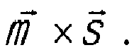
m is a magnetization direction of a free magnetic layer, and thes includes a

m has perpendicular magnetic anisotropy and is a z-axis direction, the
s may reverse a magnetization of the free magnetic layer or may move a magnetic domain structure. The direction of the spin components may be changed according to the direction of the in-plane current to reverse the magnetization of the free magnetic layer. -
FIG. 3 illustrates x-direction component sx of spin current of a magnetic tunnel junction according to a prior art and a magnetic tunnel junction according to an example embodiment of the present disclosure. - Referring to
FIGS. 2A and2B , amagnetic tunnel junction 101 includes a freemagnetic body 120 having a structure in which aunit structure 120a including [auxiliary freemagnetic layer 122a/freenon-magnetic layer 124a] are repeated N times. -
FIG. 3 illustrates the x-direction component sx of the spin current calculated quantum-mechanically based on the non-equilibrium Green's function (NEGF) technique with respect to a thickness-direction axis (z-axis) of a free magnetic body. The sx is a local value calculated at a specific z, and a boundary between the freemagnetic body 120 and theconducting wire 110 is disposed at z=0. - Referring to
FIG. 1 , in the case of the existingmagnetic tunnel junction 10, a ferromagnetic coherence length λ c is very short. Therefore, a spin component sx is almost zero within a period shorter than 1 nm from a surface of a free magnetic body (z=0). This means that a spin-orbit spin torque is a surface torque at the existing magnetic tunnel junction. - Referring to
FIG. 2 , in the case of themagnetic tunnel junction 100 according to the present disclosure, it can be understood that a spin component determining a spin-orbit spin torque is maintained in a non-zero state to a distance further away from a surface of a free magnetic body (z=0). This means that at themagnetic tunnel junction 100 according to the present disclosure, the spin-orbit spin torque is a bulk torque. -
FIG. 4 is a graph depicting a thickness average of the spin x-direction component inFIG. 3 . -
FIG. 4 illustrates the local spin component sx inFIG. 3 with reference to an average (= <sx>) of the total thickness of free magnetic bodies having different thicknesses. The <sx> is defined as below.
- The <sx> is in proportion to total spin-orbit spin torque that is actually felt by a free magnetic body having a thickness d.
- Referring to
FIG. 1 , in the existingmagnetic tunnel junction 10, a ferromagnetic coherence length λ c is very short. Therefore, the <sx> has a dependency of 1/d. That is, when the thickness d of the free magnetic body increases, spin torque efficiency decreases by about 1/d. - Referring to
FIGS. 2A and2B , in the case of themagnetic tunnel junction 100 according to the present disclosure, a dependency of <sx> on d almost does not exist. This means that spin torque efficiency is maintained even when the thickness d of the free magnetic body increases. - Hereinafter, quantum-mechanical modeling will now be described based on the non-equilibrium Green's function (NEGF) technique.
- Characteristics of a spin-orbit spin torque at a magnetic tunnel junction according to the present disclosure were confirmed based on the non-equilibrium Green's function (NEGF) technique through quantum-mechanical modeling [S. Datta, Superlattice and Microstructures 28, 4 (2000); S. Datta, Quantum transport: atom to transistor. Cambridge University Press (2005)]. Tight-binding Hamiltonian H was used for an existing magnetic tunnel junction structure of [spin polarization layer SP/non-magnetic body NM/free magnetic body (magnetic layer) FM] and a magnetic tunnel junction structure according to the present disclosure in which [spin polarization layer SP/non-magnetic body NM/free magnetic body([magnetic layer FM/non-magnetic layer NM])] is repeated. The tight-binding Hamiltonian H is given by Equations (5) to (7).


- In the Equations (5) to (7), HSP, HNM, and HFM represent Hamiltonians of layers, respectively; t represents a hopping constant, i and j represent site indexes, respectively; a† represents a creation operator; a represents an annihilation operator; Δ SP represents exchange interaction energy of a spin polarization layer;
σ represents a Pauli spin matrix; and m̂ represents a unit vector of polarization direction. At this point, Δ i represent JS of an i layer, J represents a size of exchange interaction between an angular momentumS of magnetization and a non-equilibrium spin densityS by current, and S represents |S |. - In the modeling, a spin polarization layer and a free magnetic body infinite to one side were considered by applying a surface Green's function [T. Ozaki, K. Nishio, H. Kino, Physical Review B 81, 035116 (2010)] to a self-energy matrix Λ LR. From the above-mentioned Hamiltonian and self-energy matrix, the spin density is given by Equations (8) to (10).


- In the Equations (8) to (10), G represents a Green's function, E represents energy, I represents a unit matrix, G n represents a correlation function, ρ represents an electron density, and δ
ρ represents a non-equilibrium electron density depending on application of a voltage. - To simulate that spin current depending on spin Hall effect or Rashba effect of a conducting wire has a spin of y direction, the magnetization of the spin polarization layer was set to the y direction. In the case of the existing
magnetic tunnel junction 10, a magnetization direction in all sites of the free magnetic body was set to +z direction. In the case of themagnetic tunnel junction 100 according to an example embodiment of the present disclosure, a magnetization of an odd one of magnetic layers constituting a free magnetic body was set to +z direction and a magnetization of an even magnetic layer was set to -z direction. - [Experimental Example 1] Spatial variation of non-equilibrium spin density of x component in free magnetic body of magnetic tunnel junction according to the present disclosure
- (1)
FIG. 3 illustrates an x-direction component sx of spin current calculated quantum-mechanically based on the non-equilibrium Green's function (NEGF) technique for the existingmagnetic tunnel junction 10 and themagnetic tunnel junction 100 according to the present disclosure with respect to a thickness-direction axis (z-axis) of a free magnetic body. The spin component sx is a value calculated at specific z, and a surface of the free magnetic body is disposed at z=0. - (2) Physical property values are as follows:
- Lattice spacing = 0.25 nm, thickness of magnetic layer constituting free magnetic layer = 0.25 nm, thickness of non-magnetic layer constituting free magnetic body = 0.25 nm, thickness disposed outside the free magnetic body = 2.5 nm, Hopping constant t = 1.0 eV, electronic mass = 9.1x10⁻³¹ kg, exchange energy of spin polarization layer = 0.8 eV, exchange energy of magnetic layer constituting the free magnetic body = 0.8 eV, and Fermi energy = 4.1 eV.
- (3) Referring to
FIG. 3 , in the case of the existingmagnetic tunnel junction 100, a ferromagnetic coherence length λc is very short. Therefore, the spin component is almost zero within a period shorter than 1 nm from a surface of the free magnetic body (z=0). This means that a spin-orbit spin torque is a surface torque at the existingmagnetic tunnel junction 100. - Meanwhile, in the case of the
magnetic tunnel junction 100 according to the present disclosure, sx determining a spin torque is maintained in a non-zero state to a distance further away from a surface of a free magnetic body (z=0). This means that a spin-orbit spin torque is a bulk torque at themagnetic tunnel junction 200. - [Experimental Example 2] Relationship between entire spin-orbit spin torque applied to free magnetic body of magnetic tunnel junction according to the present disclosure and thickness of the free magnetic body
- (1)
FIG. 4 illustrates the local sx inFIG. 3 with reference to an average of the total thickness of free magnetic bodies having different thicknesses. The <sx> is defined by Equation (4) and is in proportion to the entire spin-orbit spin torque felt actually by a free magnetic body having a thickness d. - (2) Physical property values are identical to those in Experimental Example 1.
- (3) Referring to
FIG. 4 , in the case of the existingmagnetic tunnel junction 10, <sx> has a dependency of 1/d. That is, when a thickness d of the free magnetic body increases, spin torque efficiency decreases by about 1/d. - Meanwhile, in the case of the
magnetic tunnel junction 100 according to the present disclosure, a dependency of <sx> on d almost does not exist. This means that spin torque efficiency is maintained even when the thickness d of the free magnetic body increases. - A dependency of critical current Ic on a thickness of a free magnetic body at a magnetic tunnel junction according to the present disclosure was confirmed through micromagnetics. An equation of motion of magnetization is given by Equation (11).

- In the Equation (11), γ represents a magnetic rotational constant, H eff represents all effective magnetic field vectors of a free magnetic field 103 or 203, α represents a Gilbert damping constant, and NSOT represents a spin-orbit spin torque.
- [Experimental Example 3] Variation of critical current Ic depending on a thickness d of a free magnetic body with respect to a magnetic tunnel junction according to the present disclosure
-
FIG. 5 illustrates variation of critical current Ic for magnetization reversal depending on a thickness d of a free magnetic body in an existing magnetic tunnel junction and a magnetic tunnel junction according to the present disclosure. - Referring to
FIG. 5 , in the case of an existingmagnetic tunnel junction 10, critical current Ic is in proportion to a thickness d. This result is obtained because spin torque efficiency has a dependency of 1/d, which is identical to a result estimated by the Equation (1). - Meanwhile, in the case of a
magnetic tunnel junction 100 according to the present disclosure, a constant result is obtained under the state that Ic is almost independent of d. This means that the intensity of current required to reverse magnetization or to move a magnetic domain structure almost does not change even when a thickness of a free magnetic body increases. - (1)
FIG. 5 illustrates variation of critical current Ic for magnetization reversal depending on a thickness d of a free magnetic body in an existingmagnetic tunnel junction 10 and amagnetic tunnel junction 100 according to the present disclosure. As shown inFIG. 5 , the critical current Ic is normalized as critical current at a thickness of d=0.6nm. In the case of the existingmagnetic tunnel junction 10, a surface torque characteristic (a non-equilibrium spin density is zero not only on a surface of a free magnetic body but also at other portions) was assumed. In the case of themagnetic tunnel junction 100 according to the present disclosure, a bulk torque characteristic (a non-equilibrium spin density is spatially uniform) was assumed. - (2) A structure of a device and physical property values are as follows.
- Common physical property of magnetic layer constituting the existing
magnetic tunnel junction 10 and magnetic layer constituting themagnetic tunnel junction 100 according to the present disclosure: "saturated magnetization value (Ms) = 1000 emu/cm3, Gilbert damping constant (α) = 0.02, perpendicular magnetic anisotropy energy (K) = 7.2x10⁶ erg/cm3, and effective spin Hall angular absolute value (|θ SH |) = 0.1" - Physical property applied to only magnetic layer constituting free magnetic layer of the
magnetic tunnel junction 100 according to present disclosure: "thickness of each magnetic layer = 0.3nm, and RKKY exchange energy between magnetic layers closest to each other = 2.5x10⁻⁷ erg/cm" - (3) Referring to
FIG. 5 , in the case of the existingmagnetic tunnel junction 10, critical current Ic is in proportion to d. This result is obtained because spin torque efficiency has a dependency of 1/d, which is identical to a result estimated by the Equation (1). - Meanwhile, in the case of the
magnetic tunnel junction 100 according to the present disclosure, a constant result is obtained under the state that Ic is almost independent of d. This means that the intensity of current required to reverse magnetization or to move a magnetic domain structure almost does not change even when a thickness of a free magnetic body increases. -
FIG. 6 illustrates variation of a thermal stability factor Δ depending on a thickness d of a free magnetic body in a magnetic tunnel junction according to the present disclosure. - Referring to
FIG. 6 , since the entire magnetic volume V increases if a thickness of a freemagnetic body 120 increases, a thermal stability factor Δ increases proportionally. - Referring to
FIGS. 5 and 6 , in the case of a magnetic tunnel junction according to an example embodiment of the present disclosure, a thermal stability factor Δ increases as a thickness d of a free magnetic body increases. However, critical current Ic is constant irrespective of d. Accordingly, when the magnetic tunnel junction according to an example embodiment of the present disclosure is used as a smaller-sized memory or logic device cell, it is driven at low current while keeping non-volatility. This characteristic makes a low-power ultrahigh-density nonvolatile device possible. - A dependency of a thermal stability factor Δ at a magnetic tunnel junction according to the present on a thickness of a free magnetic body was confirmed through a streaming technique [E. Weinan, W. Ren, E. Vanden-Eijnden, Journal of )]. To obtain an energy barrier EB that determines the thermal stability factor Δ, a transition path between two energy minimum states (case that all magnetizations are in +z direction and case that all magnetizations are in - z direction) was set first. The entire transition path was divided into 100 images. Since this initial transition path is not a minimum energy path, a minimum energy path for each ith image after passage of a time δt was obtained through Equation (12).

- In the Equation (12), γ represents a gyromagnetic constant and H eff represents all effective magnetic field vectors. Through each image converging on time, EB was determined. The thermal stability factor Δ was determined to be EB /KBT at room temperature (T = 300 K).
- [Experimental Example 4] Variation of thermal stability factor Δ depending on thickness d of free magnetic body with respect to magnetic tunnel junction according to the present disclosure
- (1)
FIG. 6 illustrates variation of a thermal stability factor Δ depending on a thickness d of a free magnetic body in amagnetic tunnel junction 100 according to the present disclosure. As shown inFIG. 6 , the thermal stability factor Δ is normalized as Δ at thickness of d=1.0nm. - (2) Structure and physical property values of device are identical to those in Experimental Example 3.
- (3) Referring to
FIG. 6 below, in the case of amagnetic tunnel junction 200 according to the present disclosure, a thermal stability factor Δ is in linear proportion to d. Since the entire magnetic volume V increases if a thickness of a free magnetic body increases, the thermal stability factor Δ increases proportionally. Therefore, this result is obtained. - The same explanations as those in
FIGS. 2 to 6 will be omitted. -
FIG. 7 illustrates a magnetic tunnel junction device according to an example embodiment of the present disclosure. - Referring to
FIG. 7 , a magnetictunnel junction device 200 includes amagnetic tunnel junction 201 including a fixedmagnetic body 240, aninsulator 130, and a freemagnetic body 120 that are sequentially stacked and aconducting wire 110 disposed adjacent to the freemagnetic body 120 of themagnetic tunnel junction 201 to apply in-plane current to themagnetic tunnel junction 201. The fixedmagnetic body 240 has a fixed magnetization direction and is a thin film including a material magnetized in a direction perpendicular to a film surface. The freemagnetic body 120 has a structure of [auxiliary freemagnetic layers 122a to 122n/freenon-magnetic layers 124a to 124n]N/main freemagnetic layer 126, where N is a positive integer greater than or equal to 2 and indicates that an [auxiliary freemagnetic layers 122a to 122n/freenon-magnetic layers 124a to 124n] structure is stacked repeatedly N times. Each of the main freemagnetic layer 126 and the auxiliary freemagnetic layers 122a to 122n changes in magnetization direction and is a thin film magnetized in a direction perpendicular to a film surface. The main freemagnetic body 120 is disposed adjacent to theconducting wire 110 that generates spin current due to the in-plane current. Among the freemagnetic layers 122a to 122n and 126 constituting the freemagnetic body 120, two magnetic layers closest to each other are magnetized in opposite directions by RKKY exchange interaction through the freemagnetic layers 124a to 124n. - The fixed
magnetic body 240 may have a synthetic antiferromagnetic structure including a first fixedmagnetic layer 244, a fixednon-magnetic layer 246, and a second fixedmagnetic layer 248 that are sequentially stacked. Each of the first fixedmagnetic layer 244 and the second fixedmagnetic layer 248 may independently include at least one of Fe, Co, Ni, B, Si, Zr, and a combination thereof. The fixednon-magnetic layer 246 may include at least one of Ru, Ta, Cu, and a combination thereof. - According to a modified embodiment of the present disclosure, the fixed
magnetic body 240 may be an exchange-biased antiferromagnetic structure including anantiferromagnetic layer 242, a first fixedmagnetic layer 244, a fixednon-magnetic layer 246, and a second fixedmagnetic layer 248 that are sequentially stacked. Theantiferromagnetic layer 242 may be formed of a material including at least one of Ir, Pt, Mn, and a combination thereof. Each of the first and second fixedmagnetic layers non-magnetic layer 246 may be formed of a material including at least one of Ru, Ta, Cu, and a combination thereof. -
FIG. 8 illustrates a magnetic tunnel junction device according to another example embodiment of the present disclosure. - Referring to
FIG. 8 , amagnetic tunnel junction 300 includes amagnetic tunnel junction 301 including a fixedmagnetic body 140, aninsulator 130, and a freemagnetic body 320 that are sequentially stacked and aconducting wire 110 disposed adjacent to the freemagnetic body 320 of themagnetic tunnel junction 301 to apply in-plane current to themagnetic tunnel junction 301. The fixedmagnetic body 140 has a fixed magnetization direction and is a thin film including a material magnetized in a direction perpendicular to a film surface. The freemagnetic body 320 has a structure of [auxiliary freemagnetic layers 322a to 322n/freenon-magnetic layers 324a to 324n]N/main free magnetic layer 326, where N is a positive integer greater than or equal to 2 and indicates that an [auxiliary freemagnetic layers 322a to 322n/freenon-magnetic layers 324a to 324n] structure (320a to 320n) is stacked repeatedly N times. Each of the main free magnetic layer 326 and the auxiliary freemagnetic layers 322a to 322n changes in magnetization direction and is a thin film magnetized in a direction perpendicular to a film surface. The main free magnetic layer 326 is disposed adjacent to theconducting wire 110 that generates spin current due to the in-plane current. Among the freemagnetic layers 322a to 322n and 326 constituting the freemagnetic body 320, two magnetic layers closest to each other are magnetized in opposite directions by RKKY exchange interaction through the freemagnetic layers 324a to 324n. - The fixed
magnetic body 140 may not be aligned with the freemagnetic body 320. Specifically, the fixedmagnetic body 140 and the freemagnetic body 320 may extend parallel to each other in an extending direction of theconducting wire 110. The freemagnetic layer 320 may include at least onemagnetic domain structure 321. Specifically, each of the main free magnetic layer 326 and the auxiliary freemagnetic layers 322a to 322n may include at least onemagnetic domain structure 321. Themagnetic domain structure 321 may move in an x axis direction due to in-plane current flowing to theconducting wire 110. Themagnetic domain structure 321 may be a magnetic domain wall or a skyrmion and may divide a magnetic domain in opposite directions. -
FIG. 9 illustrates a magnetic tunnel junction device according to another example embodiment of the present disclosure. - Referring to
FIG. 9 , amagnetic tunnel junction 400 includes amagnetic tunnel junction 101 including a fixedmagnetic body 140, aninsulator 130, and a freemagnetic body 120 that are sequentially stacked and aconducting wire 410 disposed adjacent to the freemagnetic body 120 of themagnetic tunnel junction 101 to apply in-plane current to themagnetic tunnel junction 101. The fixedmagnetic body 140 has a fixed magnetization direction and is a thin film including a material magnetized in a direction perpendicular to a film surface. The freemagnetic body 120 has a structure of [auxiliary freemagnetic layers 122a to 122n/freenon-magnetic layers 124a to 124n]N/main freemagnetic layer 126, where N is a positive integer greater than or equal to 2 and indicates that an [auxiliary freemagnetic layers 122a to 122n/freenon-magnetic layers 124a to 124n] structure (120a to 120n) is stacked repeatedly N times. Each of the main freemagnetic layer 126 and the auxiliary freemagnetic layers 122a to 122n changes in magnetization direction and is a thin film magnetized in a direction perpendicular to a film surface. The main freemagnetic layer 126 is disposed adjacent to theconducting wire 410 that generates spin current due to the in-plane current. Among the freemagnetic layers 122a to 122n and 126 constituting the freemagnetic body 320, two magnetic layers closest to each other are magnetized in opposite directions by RKKY exchange interaction through the freemagnetic layers 124a to 124n. - The
conductor 410 may include a conductive antiferromagnetic body. Specifically, theconducting wire 410 may apply in-plane current and include an antiferromagnetic layer. Theconducting wire 410 may provide an in-plane exchange bias magnetic field to the main freemagnetic layer 126. Specifically, theconducting wire 410 may be FeMn, PtMn or IrMn. The antiferromagnetic layer may provide an exchange bias magnetic field to the freemagnetic body 120. Thus, the magnetic tunnel junction device may switch a magnetization direction of a free magnetic body having perpendicular magnetic anisotropy without using an external magnetic field. -
FIG. 10 illustrates a magnetic tunnel junction device according to another example embodiment of the present disclosure. - Referring to
FIG. 10 , a magnetictunnel junction device 500 includes amagnetic tunnel junction 101 including a fixedmagnetic body 140, aninsulator 130, and a freemagnetic body 120 that are sequentially stacked and aconducting wire 510 disposed adjacent to the freemagnetic body 120 of themagnetic tunnel junction 101 to apply in-plane current to themagnetic tunnel junction 101. The fixedmagnetic body 140 has a fixed magnetization direction and is a thin film including a material magnetized in a direction perpendicular to a film surface. The freemagnetic body 120 has a structure of [auxiliary freemagnetic layers 122a to 122n/freenon-magnetic layers 124a to 124n]N/main freemagnetic layer 126, where N is a positive integer greater than or equal to 2 and indicates that an [auxiliary freemagnetic layers 122a to 122n/freenon-magnetic layers 124a to 124n] structure (120a to 120n) is stacked repeatedly N times. Each of the main freemagnetic layer 126 and the auxiliary freemagnetic layers 122a to 122n changes in magnetization direction and is a thin film magnetized in a direction perpendicular to a film surface. The main freemagnetic layer 126 is disposed adjacent to theconducting wire 410 that generates spin current due to the in-plane current. Among the freemagnetic layers 122a to 122n and 126 constituting the freemagnetic body 320, two magnetic layers closest to each other are magnetized in opposite directions by RKKY exchange interaction through the freemagnetic layers 124a to 124n: - The
conducting wire 510 applying the in-plane current may include anantiferromagnetic layer 510a and aferromagnetic layer 510b that are sequentially stacked. Theantiferromagnetic layer 510a may be disposed adjacent to the main freemagnetic layer 126. Theferromagnetic layer 510b may have an in-plane magnetization direction or a magnetization direction in which theferromagnetic layer 510b extends. Theconducting wire 510 may provide an in-plane exchange bias magnetic field to the main freemagnetic layer 126. The freemagnetic body 120 may be switched without using an external magnetic field. - The
ferromagnetic layer 510b has in-plane magnetic anisotropy and provides a function to antiferromagnetically align theantiferromagnetic layer 510a in an in-plane direction. Theantiferromagnetic layer 510a adjacent to the freemagnetic body 120 having perpendicular magnetic anisotropy establishes an exchange bias magnetic field of a direction perpendicular to the freemagnetic body 120 having the perpendicular magnetic anisotropy. Specifically, during thermal annealing under a horizontal magnetic field, theferromagnetic layer 510b is antiferromagnetically aligned with theantiferromagnetic layer 510a in the in-plane direction by exchange interaction between theantiferromagnetic layer 510b having in-plane magnetic anisotropy and theantiferromagnetic layer 510a. Thus, an exchange bias magnetic field of a horizontal direction is induced to the freemagnetic body 120 having perpendicular magnetic anisotropy adjacent to an opposite side by an antiferromagnetic rule. Current flowing to theconducting wire 510 including theantiferromagnetic layer 510a generates a spin-orbit spin torque through anomalous Hall effect or spin Hall effect. -
FIG. 11 illustrates a magnetic tunnel junction device according to another example embodiment of the present disclosure. - Referring to
FIG. 11 , a magnetictunnel junction device 600 includes amagnetic tunnel junction 601 including a fixedmagnetic body 140, aninsulator 130, and a freemagnetic body 120 that are sequentially stacked and aconducting wire 110 disposed adjacent to the freemagnetic body 120 of themagnetic tunnel junction 101 to apply in-plane current to themagnetic tunnel junction 101. The fixedmagnetic body 140 has a fixed magnetization direction and is a thin film including a material magnetized in a direction perpendicular to a film surface. The freemagnetic body 120 has a structure of [auxiliary freemagnetic layers 122a to 122n/freenon-magnetic layers 124a to 124n]N/main freemagnetic layer 126, where N is a positive integer greater than or equal to 2 and indicates that an [auxiliary freemagnetic layers 122a to 122n/freenon-magnetic layers 124a to 124n] structure (120a to 120n) is stacked repeatedly N times. Each of the main freemagnetic layer 126 and the auxiliary freemagnetic layers 122a to 122n changes in magnetization direction and is a thin film magnetized in a direction perpendicular to a film surface. The main freemagnetic layer 126 is disposed adjacent to theconducting wire 110 that generates spin current due to the in-plane current. Among the freemagnetic layers 122a to 122n and 126 constituting the freemagnetic body 320, two magnetic layers closest to each other are magnetized in opposite directions by RKKY exchange interaction through the freemagnetic layers 124a to 124n. - A dipole filed
non-magnetic layer 652 and a dipole fieldferromagnetic layer 654 having an in-plane magnetization direction are sequentially stacked adjacent to the fixedmagnetic body 140. The dipole fieldnon-magnetic layer 652 is disposed adjacent to the fixedmagnetic body 140. - The dipole field
non-magnetic layer 652 may be a conductive metal layer including at least one of Ru, Ta, Cu, and a combination thereof. - The dipole field
ferromagnetic layer 654 may have an in-plane magnetization direction (e.g., -x axis direction) and may establish a dipole magnetic field a dipole magnetic field to establish a magnetic field at the freemagnetic body 120 in an in-plane direction (+x axis direction). Thus, the freemagnetic body 120 of the magnetictunnel junction device 600 may perform magnetization reversal without using an external magnetic field. -
FIG. 12 illustrates a magnetic tunnel junction device according to another example embodiment of the present disclosure. - Referring to
FIG. 12 , a magnetictunnel junction device 700 includes amagnetic tunnel junction 701 including a fixedmagnetic body 140, aninsulator 130, and a freemagnetic body 120 that are sequentially stacked and aconducting wire 110 disposed adjacent to the freemagnetic body 120 of themagnetic tunnel junction 701 to apply in-plane current to themagnetic tunnel junction 701. The fixedmagnetic body 140 has a fixed magnetization direction and is a thin film including a material magnetized in a direction perpendicular to a film surface. The freemagnetic body 120 has a structure of [auxiliary freemagnetic layers 122a to 122n/freenon-magnetic layers 124a to 124n]N/main freemagnetic layer 126, where N is a positive integer greater than or equal to 2 and indicates that an [auxiliary freemagnetic layers 122a to 122n/freenon-magnetic layers 124a to 124n] structure (120a to 120n) is stacked repeatedly N times. Each of the main freemagnetic layer 126 and the auxiliary freemagnetic layers 122a to 122n changes in magnetization direction and is a thin film magnetized in a direction perpendicular to a film surface. The main freemagnetic layer 126 is disposed adjacent to theconducting wire 110 that generates spin current due to the in-plane current. Among the freemagnetic layers 122a to 122n and 126 constituting the freemagnetic body 320, two magnetic layers closest to each other are magnetized in opposite directions by RKKY exchange interaction through the freemagnetic layers 124a to 124n. - An auxiliary insulating
layer 727 is disposed between theconducting wire 110 and the freemagnetic body 120. The auxiliaryinsulating layer 727 may include at least one of AlOx, MgO, TaOx, ZrOx, and a combination thereof. The auxiliary insulating layer may prevent in-plane charge current flowing along theconducting wire 110 from directly flowing through themagnetic tunnel junction 701 and allows only sure spin current to pass therethrough. -
FIG. 13 illustrates a magnetic tunnel junction device according to another example embodiment of the present disclosure. - Referring to
FIG. 13 , a magnetictunnel junction device 800 includes amagnetic tunnel junction 101 including a fixedmagnetic body 140, aninsulator 130, and a freemagnetic body 120 that are sequentially stacked and aconducting wire 810 disposed adjacent to the freemagnetic body 120 of themagnetic tunnel junction 101 to apply in-plane current to themagnetic tunnel junction 101. The fixedmagnetic body 140 has a fixed magnetization direction and is a thin film including a material magnetized in a direction perpendicular to a film surface. The freemagnetic body 120 has a structure of [auxiliary freemagnetic layers 122a to 122n/freenon-magnetic layers 124a to 124n]N/main freemagnetic layer 126, where N is a positive integer greater than or equal to 2 and indicates that an [auxiliary freemagnetic layers 122a to 122n/freenon-magnetic layers 124a to 124n] structure (120a to 120n) is stacked repeatedly N times. Each of the main freemagnetic layer 126 and the auxiliary freemagnetic layers 122a to 122n changes in magnetization direction and is a thin film magnetized in a direction perpendicular to a film surface. The main freemagnetic layer 126 is disposed adjacent to theconducting wire 810 that generates spin current due to the in-plane current. Among the freemagnetic layers 122a to 122n and 126 constituting the freemagnetic body 320, two magnetic layers closest to each other are magnetized in opposite directions by RKKY exchange interaction through the freemagnetic layers 124a to 124n. - The
conducting wire 810 may include a conducting wirenon-magnetic layer 810a and a conducting wireferromagnetic layer 810b that are sequentially stacked. The conducting wireferromagnetic layer 810b may include an in-plane magnetization direction component. The conducting wirenon-magnetic layer 810a may be disposed adjacent to the freemagnetic body 120. The conducting wirenon-magnetic layer 810a may include one material selected from Cu, Ta, Pt, W, Bi, Ir, Mn, Ti, Cr, and a combination thereof. The conducting wireferromagnetic layer 810b may include at least one of Fe, Co, Ni, B, Si, Zr, and a combination thereof. Spin current may be generated through anomalous Hall effect or anisotropic magnetoresistance effect of the conducting wireferromagnetic layer 810b by the in-plane charge current flowing through the conducting wireferromagnetic layer 810b [T. Taniguchi, J. Grollier, M. D. Stiles, )]. Alternatively, the spin current may be generated by effect of interface spin-orbit coupling [V. P. Amin, M. D. Stiles, )]. -
FIG. 14 illustrates a magnetic tunnel junction device according to another example embodiment of the present disclosure. - Referring to
FIG. 14 , a magnetictunnel junction device 900 includes amagnetic tunnel junction 901 including a fixedmagnetic body 140, aninsulator 130, and a freemagnetic body 120 that are sequentially stacked and aconducting wire 910 disposed adjacent to the freemagnetic body 120 of themagnetic tunnel junction 101 to apply in-plane current to themagnetic tunnel junction 901. The fixedmagnetic body 140 has a fixed magnetization direction and is a thin film including a material magnetized in a direction perpendicular to a film surface. The freemagnetic body 120 has a structure of [auxiliary freemagnetic layers 122a to 122n/freenon-magnetic layers 124a to 124n]N/main freemagnetic layer 126, where N is a positive integer greater than or equal to 2 and indicates that an [auxiliary freemagnetic layers 122a to 122n/freenon-magnetic layers 124a to 124n] structure (120a to 120n) is stacked repeatedly N times. Each of the main freemagnetic layer 126 and the auxiliary freemagnetic layers 122a to 122n changes in magnetization direction and is a thin film magnetized in a direction perpendicular to a film surface. The main freemagnetic layer 126 is disposed adjacent to theconducting wire 910 that generates spin current due to the in-plane current. Among the freemagnetic layers 122a to 122n and 126 constituting the freemagnetic body 320, two magnetic layers closest to each other are magnetized in opposite directions by RKKY exchange interaction through the freemagnetic layers 124a to 124n. - The
conducting wire 910 may include a conducting wirenon-magnetic layer 910a and a conducting wireferromagnetic layer 910b that are sequentially stacked. Anon-magnetic layer 927 may be provided between the conductiveferromagnetic layer 910a and the freemagnetic body 120. The conducting wireferromagnetic layer 910a may be disposed adjacent to the freemagnetic body 120. Thenon-magnetic layer 927 may be aligned with a side surface of the freemagnetic body 120. - The conducting wire
non-magnetic layer 910b and thenon-magnetic layer 927 may include one material selected from Cu, Ta, Pt, W, Bi, Ir, Mn, Ti, Cr, and a combination thereof. The conducting wireferromagnetic layer 910a may include at least one of Fe, Co, Ni, B, Si, Zr, and a combination thereof. -
FIG. 15 illustrates a magnetic memory device according to an example embodiment of the present disclosure. - Referring to
FIG. 15 , amagnetic memory device 91 includes a plurality ofmagnetic tunnel junctions 101. Themagnetic tunnel junction 101 or amagnetic tunnel junction 100 may be variously modified as described with reference toFIGS. 2 to 14 . - The
magnetic memory device 91 includes a plurality ofmagnetic tunnel junctions 101 arranged on a substrate placement plane in a matrix format and a firstconductive pattern 110 disposed adjacent to a freemagnetic body 120 of themagnetic tunnel junction 101. A fixedmagnetic body 140 has a fixed magnetization direction and is a thin film formed of a material magnetized in a direction perpendicular to a film surface. The freemagnetic body 120 changes in a magnetization direction and is a thin film formed of a material magnetized in a direction perpendicular to a film surface. The freemagnetic body 120 has a structure of [auxiliary free magnetic layer/free non-magnetic layer]N/main free magnetic layer, where N is a positive integer greater than or equal to 2 and indicates that an [auxiliary free magnetic layer/free non-magnetic layer] structure is stacked repeatedly N times. Among the freemagnetic layers 122a to 122n and 126 constituting the freemagnetic body 120, two magnetic layers closest to each other are magnetized in opposite directions by RKKY exchange interaction through freemagnetic layers 124a to 124n. Themagnetic tunnel junction 101 may include a fixed magnetic body, an insulator, and a free magnetic body that are sequentially stacked. - The main free
magnetic layer 126 may be disposed adjacent to the firstconductive pattern 110, and the firstconductive pattern 110 may generate spin current from in-plane current to switch a magnetization direction of the freemagnetic body 120. - The total thickness of the free
magnetic body 120 is 2 nm or more to secure high thermal stability. - N is a positive integer greater than or equal to 2, and adjacent auxiliary free magnetic layers may have magnetizations of opposite directions in the free
magnetic body 120 by Ruderman-Kittel-Kasuya-Yosida (RKKY) exchange interaction. The entire thickness of the freemagnetic body 120 may be 2 nm or more. The auxiliary free magnetic layer and the main free magnetic layer may be formed of different materials or may have different thicknesses, respectively. Each of the auxiliary free magnetic layer and the main free magnetic layer may have a thickness of about 0.3 nm. - The first
conductive pattern 110 may be formed of one material selected from Cu, Ta, Pt, W, Bi, Ir, Mn, Ti, Cr, and a combination thereof. The firstconductive pattern 110 may provide spin current to the free magnetic layer and may apply a spin-orbit spin torque to the freemagnetic body 120. The spin-orbit spin torque may contribute to magnetization reversal of the freemagnetic body 120. - The first
conductive patterns 110 or BL may run parallel on a substrate plane in a first direction. A freemagnetic body 120 of each of the magnetic tunnel junctions arranged in the first direction may be periodically arranged adjacent to the firstconductive pattern 110. A secondconductive pattern 182 or WL may be electrically connected to a fixedmagnetic body 140 of each of themagnetic tunnel junctions 101 arranged in a second direction perpendicular to the first direction and may extend on the substrate plane in the second direction. - The
magnetic memory device 91 may operate as a cross-point memory. Themagnetic memory device 91 may operate due to spin Hall effect generated by current flowing to the firstconductive pattern 110 and critical current damping effect generated by a voltage applied to the secondconductive pattern 182. Alternatively, themagnetic memory device 91 may operate due to spin Hall effect generated by current flowing to the firstconductive pattern 110 and spin-transfer torque effect generated by current flowing through a selected magnetic tunnel junction. -
FIG. 16 illustrates a magnetic memory device according to another example embodiment of the present disclosure. - Referring to
FIG. 16 , amagnetic memory device 92 includes a plurality of magnetic tunnel junctions. Themagnetic memory device 92 includes a plurality ofmagnetic tunnel junctions 101 arranged on a substrate placement plane in a matrix format and a firstconductive pattern 110 disposed adjacent to a freemagnetic body 120 of themagnetic tunnel junction 101. A fixedmagnetic body 140 has a fixed magnetization direction and is a thin film formed of a material magnetized in a direction perpendicular to a film surface. The freemagnetic body 120 changes in a magnetization direction and is a thin film formed of a material magnetized in a direction perpendicular to a film surface. The freemagnetic body 120 has a structure of [auxiliary free magnetic layer/free non-magnetic layer]N/main free magnetic layer, where N is a positive integer greater than or equal to 2 and indicates that an [auxiliary free magnetic layer/free non-magnetic layer] structure is stacked repeatedly N times. Among the freemagnetic layers 122a to 122n and 126 constituting the freemagnetic body 120, two magnetic layers closest to each other are magnetized in opposite directions by RKKY exchange interaction through freemagnetic layers 124a to 124n. Themagnetic tunnel junction 101 may include a fixed magnetic body, an insulator, and a free magnetic body that are sequentially stacked. - The first
conductive pattern 110 may be periodically disposed to be spaced apart from a substrate plane in a first direction. A freemagnetic body 120 of each of the magnetic tunnel junctions arranged in the first direction may be periodically disposed adjacent to the firstconductive pattern 110. The firstconductive pattern 110 may provide spin current to the free magnetic layer and may apply a spin-orbit spin torque to the freemagnetic body 120. The spin-orbit spin torque may contribute to magnetization reversal of the freemagnetic body 120. - A second
conductive pattern 282 or WL is electrically connected to a fixedmagnetic body 140 of each of the magnetic tunnel junctions arranged in the first direction and extends on the substrate plane in the first direction. - A third
conductive pattern 283 or SL is connected to one end of each of the firstconductive patterns 110 arranged in the first direction and extends in the first direction. - A fourth
conductive pattern 284 or BL is connected to the other end of each of the firstconductive patterns 110 arranged in the second direction and extends in the second direction. - The
magnetic memory device 92 may operate as a modified cross-point memory. The firstconductive pattern 110 may be divided to inject spin current to the freemagnetic body 120. When current flows through the thirdconductive pattern 283, the firstconductive pattern 110, and the fourthconductive pattern 284, in-plane current flowing to the firstconductive pattern 110 may contribute to magnetization reversal of the freemagnetic body 120 by injecting the spin current into the freemagnetic body 120. -
FIG. 17 illustrates a magnetic memory device according to another example embodiment of the present disclosure. - Referring to
FIG. 17 , amagnetic memory device 93 includes a plurality of magnetic tunnel junctions. Themagnetic memory device 93 includes a plurality ofmagnetic tunnel junctions 101 arranged in a matrix format and a firstconductive pattern 110 disposed adjacent to a freemagnetic body 120 of themagnetic tunnel junction 101. A fixedmagnetic body 140 has a fixed magnetization direction and is a thin film formed of a material magnetized in a direction perpendicular to a film surface. The freemagnetic body 120 changes in a magnetization direction and is a thin film formed of a material magnetized in a direction perpendicular to a film surface. The freemagnetic body 120 has a structure of [auxiliary free magnetic layer/free non-magnetic layer]N/main free magnetic layer, where N is a positive integer greater than or equal to 2 and indicates that an [auxiliary free magnetic layer/free non-magnetic layer] structure is stacked repeatedly N times. Among the freemagnetic layers 122a to 122n and 126 constituting the freemagnetic body 120, two magnetic layers closest to each other are magnetized in opposite directions by RKKY exchange interaction through freemagnetic layers 124a to 124n. Themagnetic tunnel junction 101 may include a fixed magnetic body, an insulator, and a free magnetic body that are sequentially stacked. - The first
conductive pattern 110 may extend on a substrate plane in a first direction, and a freemagnetic body 120 of each of the magnetic tunnel junctions arranged in the first direction may be periodically disposed adjacent to the firstconductive pattern 110 or BL. The firstconductive pattern 110 may provide spin current to the free magnetic layer and may apply spin-orbit spin torque to the freemagnetic body 120. The spin-orbit spin torque may contribute to magnetization reversal of the freemagnetic body 120. - Selection transistors TR may be electrically connected to fixed
magnetic bodies 140 of themagnetic tunnel junctions 101, respectively. - A second
conductive pattern 382 or SL may be electrically connected to a source/drain of each of the selection transistors arranged in the first direction and may extend on the substrate plane in the first direction. - A third
conductive pattern 383 or WL may be connected to a gate of each of selection transistors arranged in a second direction perpendicular to the first direction. - When current flows to a specific first conductive pattern 110 (BL0), free magnetic layers of all magnetic tunnel junctions connected to the first
conductive pattern 110 may receive spin current. On the other hand, a voltage is applied to a specific third conductive pattern connected to a gate of the selection transistor TR to select a specific memory cell. Accordingly, a specific memory cell may receive spin current generated by the first conductive pattern and may receive a voltage or spin-transfer current generated by a fixed magnetic layer due to the selected selection transistor. As a result, the specific memory cell may perform a write operation. -
FIG. 18 illustrates a magnetic memory device according to another example embodiment of the present disclosure. - Referring to
FIG. 18 , amagnetic memory device 94 includes a plurality of magnetic tunnel junctions. Themagnetic memory device 94 includes a plurality ofmagnetic tunnel junctions 101 arranged in a matrix format and a firstconductive pattern 110 disposed adjacent to a freemagnetic body 120 of themagnetic tunnel junction 101. A fixedmagnetic body 140 has a fixed magnetization direction and is a thin film formed of a material magnetized in a direction perpendicular to a film surface. The freemagnetic body 120 changes in a magnetization direction and is a thin film formed of a material magnetized in a direction perpendicular to a film surface. The freemagnetic body 120 has a structure of [auxiliary free magnetic layer/free non-magnetic layer]N/main free magnetic layer, where N is a positive integer greater than or equal to 2 and indicates that an [auxiliary free magnetic layer/free non-magnetic layer] structure is stacked repeatedly N times. Among the freemagnetic layers 122a to 122n and 126 constituting the freemagnetic body 120, two magnetic layers closest to each other are magnetized in opposite directions by RKKY exchange interaction through freemagnetic layers 124a to 124n. Themagnetic tunnel junction 101 may include a fixed magnetic body, an insulator, and a free magnetic body that are sequentially stacked. - The first
conductive pattern 110 or WBL may extend on a substrate plane in a first direction, and a freemagnetic body 120 of each of the magnetic tunnel junctions arranged in the first direction may be periodically disposed adjacent to the firstconductive pattern 110. The firstconductive pattern 110 may provide spin current to the free magnetic layer and may apply a spin-orbit spin torque to the freemagnetic body 120. The spin-orbit spin torque may contribute to magnetization reversal of the freemagnetic body 120. - Selection transistors TR may be electrically connected to fixed
magnetic bodies 140 of themagnetic tunnel junctions 101, respectively. - A second
conductive pattern 482 or RBL may be electrically connected to a source/drain of each of selection transistors TR arranged in a second direction perpendicular to the first direction and may extend on the substrate plane in the second direction. - A third
conductive pattern 483 or WL may be connected to a gate of each of the selection transistor arranged in the first direction. - To perform a write operation on a specific memory cell, a specific first conductive pattern is selected and current flows to the selected first conductive pattern. In addition, a third conductive pattern connected to a gate of a selection transistor connected to the selected memory cell is selected, so a voltage is applied to the fixed magnetic layer or spin-transfer current flows to the fixed magnetic layer. As a result, the specific memory cell may perform a write operation.
-
FIG. 19 illustrates a magnetic memory device according to another example embodiment of the present disclosure. - Referring to
FIG. 19 , amagnetic memory device 95 includes a plurality of magnetic tunnel junctions. Themagnetic memory device 95 includes a plurality ofmagnetic tunnel junctions 101 arranged in a matrix format and a firstconductive pattern 110 disposed adjacent to a freemagnetic body 120 of themagnetic tunnel junction 101. A fixedmagnetic body 140 has a fixed magnetization direction and is a thin film formed of a material magnetized in a direction perpendicular to a film surface. The freemagnetic body 120 changes in a magnetization direction and is a thin film formed of a material magnetized in a direction perpendicular to a film surface. The freemagnetic body 120 has a structure of [auxiliary free magnetic layer/free non-magnetic layer]N/main free magnetic layer, where N is a positive integer greater than or equal to 2 and indicates that an [auxiliary free magnetic layer/free non-magnetic layer] structure is stacked repeatedly N times. Among the freemagnetic layers 122a to 122n and 126 constituting the freemagnetic body 120, two magnetic layers closest to each other are magnetized in opposite directions by RKKY exchange interaction through freemagnetic layers 124a to 124n. Themagnetic tunnel junction 101 may include a fixedmagnetic body 140, aninsulator 130, and a freemagnetic body 120 that are sequentially stacked. - The first
conductive pattern 110 or WBL may extend on a substrate plane in a first direction, and a freemagnetic body 120 of each of the magnetic tunnel junctions arranged in the first direction may be periodically disposed adjacent to the firstconductive pattern 110. The firstconductive pattern 110 may provide spin current to the free magnetic layer and may apply a spin-orbit spin torque to the freemagnetic body 120. The spin-orbit spin torque may contribute to magnetization reversal of the freemagnetic body 120. - A second
conductive pattern 582 or RBL may be electrically connected to a fixedmagnetic body 140 of each of the magnetic tunnel junctions arranged in the first direction and may extend in the first direction. - A third
conductive pattern 583 or WBL may be connected to one end of each of the firstconductive patterns 110 arranged in the first direction and may extend in the first direction. - Selection transistors may be connected to the other ends of the first
conductive patterns 110, respectively. - A fourth
conductive pattern 584 or SL may be connected to a source/drain of each of the selection transistors TR arranged in the first direction and may extend in the first direction. - A fifth
conductive pattern 585 or WL may be connected to a gate of each of selection transistors arranged in a second direction perpendicular to the first direction and may extend in the second direction. -
FIG. 20 illustrates a magnetic memory device according to another example embodiment of the present disclosure. - Referring to
FIG. 20 , amagnetic memory device 96 includes a plurality of magnetic tunnel junctions. Themagnetic memory device 96 includes a plurality ofmagnetic tunnel junctions 101 arranged in a matrix format and a firstconductive pattern 110 disposed adjacent to a freemagnetic body 120 of themagnetic tunnel junction 101. A fixedmagnetic body 140 has a fixed magnetization direction and is a thin film formed of a material magnetized in a direction perpendicular to a film surface. The freemagnetic body 120 changes in a magnetization direction and is a thin film formed of a material magnetized in a direction perpendicular to a film surface. The freemagnetic body 120 has a structure of [auxiliary free magnetic layer/free non-magnetic layer]N/main free magnetic layer, where N is a positive integer greater than or equal to 2 and indicates that an [auxiliary free magnetic layer/free non-magnetic layer] structure is stacked repeatedly N times. Among the freemagnetic layers 122a to 122n and 126 constituting the freemagnetic body 120, two magnetic layers closest to each other are magnetized in opposite directions by RKKY exchange interaction through freemagnetic layers 124a to 124n. Themagnetic tunnel junction 101 may include a fixedmagnetic body 140, aninsulator 130, and a freemagnetic body 120 that are sequentially stacked. - The first
conductive pattern 110 or WBL may extend on a substrate plane in a first direction, and a freemagnetic body 120 of each of the magnetic tunnel junctions arranged in the first direction may be periodically disposed adjacent to the firstconductive pattern 110. The firstconductive pattern 110 may provide spin current to the free magnetic layer and may apply a spin-orbit spin torque to the freemagnetic body 120. The spin-orbit spin torque may contribute to magnetization reversal of the freemagnetic body 120. - Selection transistors TR may be connected to fixed
magnetic body 140 of themagnetic tunnel junctions 101, respectively. - A second
conductive pattern 682 or RBL may be connected to a source/drain of each of the selection transistors TR arranged in the first direction and may extend in the first direction. - A third
conductive pattern 683 or WL may be connected to a gate of each of selection transistors TR arranged in a second direction perpendicular to the first direction and may extend in the second direction. - A fourth
conductive pattern 684 or WBL may be connected to one end of each of the firstconductive pattern 110 arranged in the first direction and may extend in the first direction. - A fourth
conductive pattern 685 or SL may be connected to the other end of the firstconductive pattern 110 arranged in the first direction and may extend in the first direction. -
FIG. 21 illustrates a magnetic memory device according to another example embodiment of the present disclosure. - Referring to
FIG. 21 , amagnetic memory device 97 includes a plurality of magnetic tunnel junctions. Themagnetic memory device 97 includes a plurality ofmagnetic tunnel junctions 101 arranged in a matrix format and a firstconductive pattern 110 disposed adjacent to a freemagnetic body 120 of themagnetic tunnel junction 101. A fixedmagnetic body 140 has a fixed magnetization direction and is a thin film formed of a material magnetized in a direction perpendicular to a film surface. The freemagnetic body 120 changes in a magnetization direction and is a thin film formed of a material magnetized in a direction perpendicular to a film surface. The freemagnetic body 120 has a structure of [auxiliary free magnetic layer/free non-magnetic layer]N/main free magnetic layer, where N is a positive integer greater than or equal to 2 and indicates that an [auxiliary free magnetic layer/free non-magnetic layer] structure is stacked repeatedly N times. Among the freemagnetic layers 122a to 122n and 126 constituting the freemagnetic body 120, two magnetic layers closest to each other are magnetized in opposite directions by RKKY exchange interaction through freemagnetic layers 124a to 124n. Themagnetic tunnel junction 101 may include a fixedmagnetic body 140, aninsulator 130, and a freemagnetic body 120 that are sequentially stacked. - The first
conductive pattern 110 or WBL may extend on a substrate plane in a first direction, and a freemagnetic body 120 of each of the magnetic tunnel junctions arranged in the first direction may be periodically disposed adjacent to the firstconductive pattern 110. The firstconductive pattern 110 may provide spin current to the free magnetic layer and may apply a spin-orbit spin torque to the freemagnetic body 120. The spin-orbit spin torque may contribute to magnetization reversal of the freemagnetic body 120. - A second
conductive pattern 782 may be electrically connected to each of fixedmagnetic bodies 140 of themagnetic tunnel junctions 101 arranged in the first direction and may extend in the second direction. - A first selection transistor TR1 may be connected to one end of each of the first
conductive patterns 110. - A second selection transistor TR2 may be connected to the other end of each of the first
conductive patterns 110. - A third
conductive pattern 783 or WBL may be connected to a source/drain of the first selection transistor TR1 disposed in the first direction and may extend in the first direction. - A fourth
conductive pattern 784 or SL may be connected to a source/drain of the second transistor TR2 disposed in the first direction and may extend in the first direction. - A fifth
conductive pattern 785 may extend in the second direction by connecting a gate of the first selection transistor TR1 disposed in a second direction perpendicular to the first direction and a gate of the second selection transistor TR2 to each other. -
FIG. 22 illustrates a magnetic memory device according to another example embodiment of the present disclosure. - Referring to
FIG. 21 , amagnetic memory device 98 includes a plurality of magnetic tunnel junctions. Themagnetic memory device 98 includes a plurality ofmagnetic tunnel junctions 101 arranged in a matrix format and a firstconductive pattern 110 disposed adjacent to a freemagnetic body 120 of themagnetic tunnel junction 101. A fixedmagnetic body 140 has a fixed magnetization direction and is a thin film formed of a material magnetized in a direction perpendicular to a film surface. The freemagnetic body 120 changes in a magnetization direction and is a thin film formed of a material magnetized in a direction perpendicular to a film surface. The freemagnetic body 120 has a structure of [auxiliary free magnetic layer/free non-magnetic layer]N/main free magnetic layer, where N is a positive integer greater than or equal to 2 and indicates that an [auxiliary free magnetic layer/free non-magnetic layer] structure is stacked repeatedly N times. Among the freemagnetic layers 122a to 122n and 126 constituting the freemagnetic body 120, two magnetic layers closest to each other are magnetized in opposite directions by RKKY exchange interaction through freemagnetic layers 124a to 124n. Themagnetic tunnel junction 101 may include a fixedmagnetic body 140, aninsulator 130, and a freemagnetic body 120 that are sequentially stacked. - The first
conductive pattern 110 or WBL may extend on a substrate plane in a first direction, and a freemagnetic body 120 of each of the magnetic tunnel junctions arranged in the first direction may be periodically disposed adjacent to the firstconductive pattern 110. The firstconductive pattern 110 may provide spin current to the free magnetic layer and may apply a spin-orbit spin torque to the freemagnetic body 120. The spin-orbit spin torque may contribute to magnetization reversal of the freemagnetic body 120. - A first selection transistor TR1 may be connected to each of fixed
magnetic bodies 140 of themagnetic tunnel junctions 101. - A second selection transistor TR2 may be connected to one end of each of the first
conductive patterns 110. - A second
conductive pattern 882 or RBL may be connected to a source/drain of the first selection transistor TR1 disposed in the first direction and may extend in the first direction. - A third
conductive pattern 883 or WBL may connect the other ends of the firstconductive patterns 110 arranged in the first direction to each other and extend in the first direction. - A fourth
conductive pattern 884 or SL may connect sources/drains of the second selection transistors TR2 arranged in the first direction to each other and may extend in the first direction. - A fifth
conductive pattern 885 or WL may connect gates of first selection transistors arranged in a second direction perpendicular to the first direction to each other and may extend in the second direction. - A sixth
conductive pattern 886 or WL may connect gates of the second selection transistors arranged in the second direction to each other and may extend in the second direction. - Referring to
FIGS. 15 to 21 andFIG. 8 , the freemagnetic body 120 may include at least one magnetic domain structure. The magnetic domain structure may be a magnetic domain wall or a skyrmion. - Referring to
FIGS. 15 to 21 andFIG. 9 , the firstconductive pattern 110 may apply in-plane current and include an antiferromagnetic layer. The firstconductive pattern 110 may provide an in-plane exchange bias magnetic field to the main free magnetic layer. - Referring to
FIGS. 15 to 21 andFIG. 10 , the firstconductive pattern 110 may apply in-plane current and include an antiferromagnetic layer and a ferromagnetic layer that are sequentially stacked. The antiferromagnetic layer is disposed adjacent to the main free magnetic layer, the ferromagnetic layer has an in-plane magnetization direction, the first conductive pattern provides an in-plane exchange bias magnetic field to the main free magnetic layer, and the free magnetic body may be switched without an external magnetic field. - Referring to
FIGS. 15 to 21 andFIG. 11 , a dipole field non-magnetic layer and a dipole field ferromagnetic layer having an in-plane magnetization direction, which are sequentially stacked adjacent to the fixed magnetic body, may be further provided. The non-magnetic layer may be disposed adjacent to the fixed magnetic body. The free magnetic body may be switched without an external magnetic field by an in-plane magnetic field provided from the dipole field ferromagnetic layer. - Referring to
FIGS. 15 to 21 andFIG. 12 , an auxiliary insulating layer may be further provided between the firstconductive pattern 110 and the freemagnetic body 120. - Referring to
FIGS. 15 to 21 andFIG. 13 , the firstconductive pattern 110 may include a first conductive pattern non-magnetic layer and a first conductive pattern magnetic layer that are sequentially stacked, and the first conductive pattern magnetic layer may include an in-plane magnetization direction component. - Referring to
FIGS. 15 to 21 andFIG. 14 , the firstconductive pattern 110 may include a first conductive pattern magnetic layer and a first conductive pattern non-magnetic layer that are sequentially stacked and may include a non-magnetic layer disposed between the first conductive pattern magnetic layer and the free magnetic body. - As described above, a magnetic tunnel junction device according to an example embodiment of the present disclosure may provide a characteristic in which efficiency of a spin-orbit spin torque is not in proportion to a thickness of a free magnetic body and is relatively irrelevant thereto, by using a characteristic in which when current flows along a conducting wire adjacent to the free magnetic body in an in-plane direction, spin current generated by spin Hall effect or Rashba effect is not entirely absorbed to a surface of the free magnetic body and is relatively uniformly absorbed throughout the thickness of the free magnetic body. Accordingly, if the total thickness d of the free magnetic body increases by increasing N of a structure of [magnetic layer/non-magnetic layer]N/magnetic layer, thermal stability is improved while critical current Ic is irrelevant to the total thickness d of the free magnetic body. Thus, non-volatility may be secured (e.g., Δ > 50) and a device may be driven through low critical current even when a magnetic tunnel junction having a very small cross-sectional area is used. As a result, a magnetic tunnel junction structure may be implemented to enable an ultrahigh nonvolatile device to be driven at low power.
- The invention includes the aspects described in the following clauses. These clauses form part of the description and are not claims.
- Clause 1: A magnetic tunnel junction device including a magnetic tunnel junction including a fixed magnetic body, an insulator, and a free magnetic body that are sequentially stacked and a conducting wire disposed adjacent to the free magnetic body of the magnetic tunnel junction to apply in-plane current to the magnetic tunnel junction,
wherein the fixed magnetic body has a fixed magnetization direction and is a thin film including a material magnetized in a direction perpendicular to a film surface,
the free magnetic body has a structure of [auxiliary free magnetic layer/free non-magnetic layer] N/main free magnetic layer,
N is a positive integer greater than or equal to 2 and indicates that an [auxiliary free magnetic layer/free non-magnetic layer] structure is stacked repeatedly N times,
two adjacent magnetic layers in the free magnetic body have opposite magnetization directions by Ruderman-Kittel-Kasuya-Yosida (RKKY) exchange interaction conducted through the free non-magnetic layer,
each of the main free magnetic layer and the auxiliary free magnetic layer changes in magnetization direction and is a thin film including a material magnetized in a direction perpendicular to a film surface, and
the main free magnetic layer is disposed adjacent to the conducting wire generating spin current by the in-plane current. - Clause 2: The magnetic tunnel junction device as set forth in
clause 1, wherein the auxiliary free magnetic layer adjacent to the insulator has a thickness of 1 nm or less. - Clause 3: The magnetic tunnel junction device as set forth in
clause 1, wherein except for the auxiliary free magnetic layer adjacent to the insulator among magnetic layers included in the free magnetic body, all magnetic layers each have a thickness of 1 nm or less. - Clause 4: The magnetic tunnel junction device as set forth in
clause 1 or any of the other previous clauses, wherein the total thickness of the free magnetic body is 2 nm or more. - Clause 5: The magnetic tunnel junction device as set forth in
clause 1 or any of the other previous clauses, wherein each of the auxiliary free magnetic layer and the main free magnetic layer includes at least one of Fe, Co, Ni, B, Si, Zr, and a combination thereof. - Clause 6: The magnetic tunnel junction device as set forth in
clause 1 or any of the other previous clauses, wherein the auxiliary free magnetic layer and the main free magnetic layer are formed of different materials or have different thicknesses. - Clause 7: The magnetic tunnel junction device as set forth in
clause 1 or any of the other previous clauses, wherein the free non-magnetic layer of the free magnetic body includes at least one of Ru, Ta, Cu, and a combination thereof. - Clause 8: The magnetic tunnel junction device as set forth in
clause 1 or any of the other previous clauses, wherein the fixed magnetic body includes at least one of Fe, Co, Ni, B, Si, Zr, and a combination thereof. - Clause 9: The magnetic tunnel junction device as set forth in
clause 1 or any of the other previous clauses, wherein the fixed magnetic body has a synthetic antiferromagnetic structure including a first fixed magnetic layer, a fixed non-magnetic layer, and a second fixed magnetic layer that are sequentially stacked,
each of the first fixed magnetic layer and the second fixed magnetic layer independently includes at least one of Fe, Co, Ni, B, Si, Zr, and a combination thereof, and
the fixed non-magnetic layer includes at least one of Ru, Ta, Cu, and a combination thereof. - Clause 10: The magnetic tunnel junction device as set forth in
clause 1 or any of the other previous clauses, wherein the first fixed magnetic body has an exchange-biased antiferromagnetic structure including an antiferromagnetic layer, a first fixed magnetic layer, a fixed non-magnetic layer, and a second fixed magnetic layer that are sequentially stacked,
the antiferromagnetic layer is formed of a material including at least one of Ir, Pt, Mn, and a combination thereof,
each of the first fixed magnetic layer and the second fixed magnetic layer is independently formed of a material including at least one of Fe, Co, Ni, B, Si, Zr, and a combination thereof, and
the fixed non-magnetic layer is formed of a material including at least one of Ru, Ta, Cu, and a combination thereof. - Clause 11: The magnetic tunnel junction device as set forth in
clause 1 or any of the other previous clauses, wherein the insulator is formed of a material including at least one of AlOx, MgO, TaOx, ZrOx, and a combination thereof. - Clause 12: The magnetic tunnel junction device as set forth in
clause 1 or any of the other previous clauses, wherein the conducting wire applying the in-plane current is formed of a material including at least one of Cu, Ta, Pt, W, Bi, Ir, Mn, Ti, Cr, O, and a combination thereof. - Clause 13: The magnetic tunnel junction device as set forth in
clause 1 or any of the other previous clauses, wherein the conducting wire applying the in-plane current includes an antiferromagnetic layer, and
the conducting wire provides an in-plane exchange bias magnetic field to the main free magnetic layer. - Clause 14: The magnetic tunnel junction device as set forth in
clause 1 or any of the other previous clauses, wherein a magnetic field established from the outside of the free magnetic body is applied to the free magnetic body. - Clause 15: The magnetic tunnel junction device as set forth in
clause 1 or any of the other previous clauses, wherein the free magnetic body includes at least one magnetic domain structure. - Clause 16: The magnetic tunnel junction device as set forth in
clause 1 or any of the other previous clauses, wherein the conducting wire applying the in-plane current includes an antiferromagnetic layer and a ferromagnetic layer that are sequentially stacked,
the antiferromagnetic layer is disposed adjacent to the main free magnetic layer,
the ferromagnetic layer has an in-plane magnetization direction,
the conducting wire provides an in-plane exchange bias magnetic field to the main free magnetic layer, and
the free magnetic body is switched without an external magnetic field. - Clause 17: The magnetic tunnel junction device as set forth in
clause 1 or any of the other previous clauses, further comprising:- a dipole field non-magnetic layer and a dipole field ferromagnetic layer having an in-plane magnetization direction that are sequentially stacked adjacent to the fixed magnetic body,
- wherein the dipole field non-magnetic layer is disposed adjacent to the fixed magnetic body, and
- the free magnetic body is switched without an external magnetic field.
- Clause 18: The magnetic tunnel junction device as set forth in
clause 1 or any of the other previous clauses, further comprising:- an auxiliary insulating layer disposed between the conducting wire and the free magnetic body.
- Clause 19: The magnetic tunnel junction device as set forth in
clause 1 or any of the other previous clauses, wherein the conducting wire includes a conducting wire non-magnetic layer and a conducting wire ferromagnetic layer that are sequentially stacked, and
the conducting wire includes an in-plane magnetization direction component. - Clause 20: The magnetic tunnel junction device as set forth in
clause 1 or any of the other previous clauses, wherein the conducting wire includes a conducting wire ferromagnetic layer and a conducting wire non-magnetic layer that are sequentially stacked, and
the conducting wire includes a non-magnetic layer disposed between the conducting wire ferromagnetic layer and the free magnetic body. - Clause 21: A magnetic memory device comprising:
- a plurality of magnetic tunnel junctions arranged in a matrix format; and
- a first conductive pattern disposed adjacent to a free magnetic body of the magnetic tunnel junction,
- wherein each of the magnetic tunnel junctions includes a fixed magnetic body, an insulator, and a free magnetic body that are sequentially stacked,
- the fixed magnetic body that has a fixed magnetization direction and is a thin film including a material magnetized in a direction perpendicular to a film surface,
- the free magnetic body changes in magnetization direction and is a thin film including a material magnetized in a direction perpendicular to a film surface,
- the free magnetic body has a structure of [auxiliary free magnetic layer/free non-magnetic layer]N/main free magnetic layer,
- two adjacent magnetic layers in the free magnetic body have opposite magnetization directions by Ruderman-Kittel-Kasuya-Yosida (RKKY) exchange interaction conducted through the free non-magnetic layer, and
- N is a positive integer greater than or equal to 2 and indicates that an [auxiliary free magnetic layer/free non-magnetic layer] structure is stacked repeatedly N times.
- Clause 22: The magnetic memory device as set forth in clause 21, wherein the main free magnetic layer is disposed adjacent to the first conductive pattern, and
the first conductive pattern generates spin current perpendicular to a placement plane of the first conductive pattern from in-plane current to switch a magnetization direction of the free magnetic body. - Clause 23: The magnetic memory device as set forth in clause 21 or clause 22, wherein the auxiliary free magnetic layer adjacent to an insulator has a thickness of 1 nm or more.
- Clause 24: The magnetic memory device as set forth in clause 21 or clause 22, wherein except for the auxiliary free magnetic layer adjacent to the insulator among magnetic layers included in the free magnetic body, all magnetic layers each have a thickness of 1 nm or less.
- Clause 25: The magnetic memory device as set forth in clause 21 or any of the clauses 22 to 24, wherein the total thickness of the free magnetic body is 2 nm or more.
- Clause 26: The magnetic memory device as set forth in clause 21 or any of the clauses 22 to 25, wherein the auxiliary free magnetic layer and the main free magnetic layer are formed of different materials or have different thicknesses.
- Clause 27: The magnetic memory device as set forth in clause 21 or any of the clauses 22 to 26, wherein the first conductive pattern is formed of a material including at least one of Cu, Ta, Pt, W, Bi, Ir, Mn, Ti, Cr, O, and a combination thereof.
- Clause 28: The magnetic memory device as set forth in clause 21 or any of the clauses 22 to 27, wherein the first conductive pattern applies in-plane current and includes an antiferromagnetic layer, and
the first conductive pattern provides an in-plane exchange bias magnetic field to the main free magnetic layer. - Clause 29: The magnetic memory device as set forth in clause 21 or any of the clauses 22 to 28, wherein the free magnetic body includes at least one magnetic domain structure.
- Clause 30: The magnetic memory device as set forth in clause 21 or any of the clauses 22 to 29, wherein the first conductive pattern applies in-plane current and includes an antiferromagnetic layer and a ferromagnetic layer that are sequentially stacked.,
the antiferromagnetic layer is disposed adjacent to the main free magnetic layer,
the ferromagnetic layer has an in-plane magnetization direction,
the first conductive pattern provides an in-plane exchange bias magnetic field to the main free magnetic layer, and
the free magnetic body is switched without an external magnetic field. - Clause 31: The magnetic memory device as set forth in clause 21 or any of the clauses 22 to 30, further comprising:
- a dipole field ferromagnetic layer including a dipole field non-magnetic layer and a dipole field ferromagnetic layer having an in-plane magnetization direction that are sequentially stacked adjacent to the fixed magnetic body,
- wherein the non-magnetic layer is disposed adjacent to the fixed magnetic body.
- Clause 32: The magnetic memory device as set forth in clause 21 or any of the clauses 22 to 31, further comprising:
- an auxiliary insulating layer disposed between the first conductive pattern and the free magnetic body.
- Clause 33: The magnetic memory device as set forth in clause 21 or any of the clauses 22 to 32, wherein the first conductive pattern includes a first conductive pattern non-magnetic layer and a first conductive magnetic layer that are sequentially stacked, and
the first conductive pattern magnetic layer includes an in-plane magnetization direction component. - Clause 34: The magnetic memory device as set forth in clause 21 or any of the clauses 22 to 33, wherein the first conductive pattern includes a first conducive pattern magnetic layer and a first conductive pattern non-magnetic layer that are sequentially stacked, and
the first conductive pattern further includes a non-magnetic layer disposed between the first conductive pattern magnetic layer and the free magnetic body. - Clause 35: The magnetic memory device as set forth in clause 21 or any of the clauses 22 to 34, wherein the first conductive pattern runs parallel on a substrate plane in a first direction, and
a free magnetic body of each of magnetic tunnel junctions arranged in the first direction is periodically disposed adjacent to the first conductive pattern,
the magnetic memory device further comprising:- a second conductive pattern that is electrically connected to a fixed magnetic body of each of magnetic tunnel junctions arranged in a second direction perpendicular to the first direction and extends on the substrate plane in the second direction.
- Clause 36: The magnetic memory device as set forth in clause 21 or any of the clauses 22 to 35, wherein the first conductive pattern is periodically disposed on a substrate plane in a first direction, and
a free magnetic body of each of magnetic tunnel junctions arranged in the first direction is periodically disposed adjacent to the first conductive pattern,
the magnetic memory device further comprising:- a second conductive pattern that is electrically connected to a fixed magnetic body of each of the magnetic tunnel junctions arranged in the first direction and extends on the substrate plane in the first direction;
- a third conductive pattern that is connected to one end of each of the first conductive patterns arranged in the first direction and extends in the first direction; and
- a fourth conductive pattern that is connected to the other end of each of the first conducive patterns arranged in the second direction and extends in the second direction.
- Clause 37: The magnetic memory device as set forth in clause 21 or any of the clauses 22 to 36, wherein the first conductive pattern extends on a substrate plane in a first direction, and
a free magnetic body of each of magnetic tunnel junctions arranged in the first direction is periodically disposed adjacent to the first conductive pattern,
the magnetic memory device further comprising:- selection transistors that are electrically connected to fixed magnetic bodies of the magnetic tunnel junctions, respectively;
- a second conductive patterns that is electrically connected to a source/drain of each of selection transistors arranged in the first direction and extends on the substrate plane in the first direction; and
- a third conductive pattern that is connected to a gate of each of selection transistors arranged in a second direction perpendicular to the first direction.
- Clause 38: The magnetic memory device as set forth in clause 21 or any of the clauses 22 to 37, wherein the first conductive pattern extends on a substrate plane in a first direction, and
a free magnetic body of each of magnetic tunnel junctions arranged in the first direction is periodically disposed adjacent to the first conductive pattern,
the magnetic memory device further comprising:- selection transistors that are electrically connected to fixed magnetic bodies of the magnetic tunnel junctions, respectively;
- a second conductive patterns that is electrically connected to a source/drain of each of selection transistors arranged in the first direction and extends on the substrate plane in the first direction; and
- a third conductive pattern that is connected to a gate of each of the selection transistors arranged in the first direction.
- Clause 39: The magnetic memory device as set forth in clause 21 or any of the clauses 22 to 38, wherein the first conductive pattern extends on a substrate plane in a first direction, and
a free magnetic body of each of magnetic tunnel junctions arranged in the first direction is periodically disposed adjacent to the first conductive pattern,
the magnetic memory device further comprising:- a second conductive pattern that is electrically connected to a fixed magnetic body of each of magnetic tunnel junctions arranged in the first direction;
- a third conductive pattern that is connected to one end of the conductive pattern disposed in the first direction;
- selection transistors connected to the other end of the first conductive pattern;
- a fourth conductive pattern that is connected to a source/drain of each of selection transistors arranged in the first direction and extends in the first direction; and
- a fourth conductive pattern that is connected to a gate of each of selection transistors arranged in a second direction perpendicular to the first direction and extends in the second direction.
- Clause 40: The magnetic memory device as set forth in clause 21 or any of the clauses 22 to 39, wherein the first conductive pattern extends on a substrate plane in a first direction, and
a free magnetic body of each of magnetic tunnel junctions arranged in the first direction is periodically disposed adjacent to the first conductive pattern,
the magnetic memory device further comprising:- selection transistors that are connected to fixed magnetic bodies of the magnetic tunnel junctions, respectively;
- a second conductive pattern that is connected to a source/drain of each of selection transistors arranged in the first direction;
- a third conductive pattern that is connected to a gate of each of selection transistors arranged in a second direction perpendicular to the first direction and extends in the second direction;
- a fourth conductive pattern that is connected to one end of the first conductive pattern disposed in the first direction; and
- a fifth conductive pattern that is connected to the other end of the first conductive pattern disposed in the first direction and extends in the first direction.
- Clause 41: The magnetic memory device as set forth in clause 21 or any of the clauses 22 to 40, wherein the first conductive pattern extends on a substrate plane in a first direction, and
a free magnetic body of each of magnetic tunnel junctions arranged in the first direction is periodically disposed adjacent to the first conductive pattern,
the magnetic memory device further comprising:- a second conductive pattern that is electrically connected to a fixed magnetic body of each of magnetic tunnel junctions arranged in the first direction;
- a first selection transistor that is connected to one end of the first conductive pattern;
- a second selection transistor connected to the other end of the first conductive pattern;
- a third conductive pattern that is connected to a source/drain of the first selection transistor disposed in the first direction and extends in the first direction;
- a fourth conductive pattern that is connected to a source/drain of the second selection transistor disposed in the first direction and extends in the first direction; and
- a fifth conductive pattern that extends in the second direction by connecting a gate of the first selection transistor disposed in a second direction perpendicular to the first direction and a gate of the second selection transistor to each other.
- Clause 42: The magnetic memory device as set forth in clause 21 or any of the clauses 22 to 41, wherein the first conductive pattern extends on a substrate plane in a first direction, and
a free magnetic body of each of magnetic tunnel junctions arranged in the first direction is periodically disposed adjacent to the first conductive pattern,
the magnetic memory device further comprising:- a first selection transistor that is connected to a fixed magnetic body of each of the magnetic tunnel junctions;
- a second selection transistor that is connected to one end of the first conductive pattern;
- a second conductive pattern that is connected to a source/drain of the first selection transistor disposed in the first direction and extends in the first direction;
- a third conductive pattern that connects the other ends of first conductive patterns arranged in the first direction to each other and extends in the first direction;
- a fourth conductive pattern that connects sources/drains of second transistors arranged in the first direction to each other and extend in the first direction;
- a fifth conductive pattern that connects gates of first selection transistors arranged in a second direction perpendicular to the first direction to each other and extends in the second direction; and
- a sixth conductive pattern that connects gates of second selection transistors arranged in the second direction to each other and extends in the second direction.
- Although the present disclosure and its advantages have been described in detail, it should be understood that various changes, substitutions and alterations can be made herein without departing from the spirit and scope of the disclosure as defined by the following claims.

Claims (15)
- A magnetic tunnel junction device including a magnetic tunnel junction including a fixed magnetic body, an insulator, and a free magnetic body that are sequentially stacked and a conducting wire disposed adjacent to the free magnetic body of the magnetic tunnel junction to apply in-plane current to the magnetic tunnel junction,
wherein the fixed magnetic body has a fixed magnetization direction and is a thin film including a material magnetized in a direction perpendicular to a film surface,
the free magnetic body has a structure of [auxiliary free magnetic layer/free non-magnetic layer]N/main free magnetic layer,
N is a positive integer greater than or equal to 2 and indicates that an [auxiliary free magnetic layer/free non-magnetic layer] structure is stacked repeatedly N times,
two adjacent magnetic layers in the free magnetic body have opposite magnetization directions by Ruderman-Kittel-Kasuya-Yosida (RKKY) exchange interaction conducted through the free non-magnetic layer,
each of the main free magnetic layer and the auxiliary free magnetic layer changes in magnetization direction and is a thin film including a material magnetized in a direction perpendicular to a film surface, and
the main free magnetic layer is disposed adjacent to the conducting wire generating spin current by the in-plane current. - The magnetic tunnel junction device as set forth in claim 1, wherein the auxiliary free magnetic layer adjacent to the insulator has a thickness of 1 nm or less.
- The magnetic tunnel junction device as set forth in claim 1, wherein except for the auxiliary free magnetic layer adjacent to the insulator among magnetic layers included in the free magnetic body, all magnetic layers each have a thickness of 1 nm or less.
- The magnetic tunnel junction device as set forth in claim 1, wherein the total thickness of the free magnetic body is 2 nm or more.
- The magnetic tunnel junction device as set forth in claim 1, wherein the auxiliary free magnetic layer and the main free magnetic layer are formed of different materials or have different thicknesses.
- The magnetic tunnel junction device as set forth in claim 1, wherein the first fixed magnetic body has an exchange-biased antiferromagnetic structure including an antiferromagnetic layer, a first fixed magnetic layer, a fixed non-magnetic layer, and a second fixed magnetic layer that are sequentially stacked,
the antiferromagnetic layer is formed of a material including at least one of Ir, Pt, Mn, and a combination thereof,
each of the first fixed magnetic layer and the second fixed magnetic layer is independently formed of a material including at least one of Fe, Co, Ni, B, Si, Zr, and a combination thereof, and
the fixed non-magnetic layer is formed of a material including at least one of Ru, Ta, Cu, and a combination thereof. - The magnetic tunnel junction device as set forth in claim 1, wherein the conducting wire applying the in-plane current is formed of a material including at least one of Cu, Ta, Pt, W, Bi, Ir, Mn, Ti, Cr, O, and a combination thereof.
- The magnetic tunnel junction device as set forth in claim 1, wherein the conducting wire applying the in-plane current includes an antiferromagnetic layer, and
the conducting wire provides an in-plane exchange bias magnetic field to the main free magnetic layer. - The magnetic tunnel junction device as set forth in claim 1, wherein a magnetic field established from the outside of the free magnetic body is applied to the free magnetic body.
- The magnetic tunnel junction device as set forth in claim 1, wherein the conducting wire applying the in-plane current includes an antiferromagnetic layer and a ferromagnetic layer that are sequentially stacked,
the antiferromagnetic layer is disposed adjacent to the main free magnetic layer,
the ferromagnetic layer has an in-plane magnetization direction,
the conducting wire provides an in-plane exchange bias magnetic field to the main free magnetic layer, and
the free magnetic body is switched without an external magnetic field. - The magnetic tunnel junction device as set forth in claim 1, further comprising:a dipole field non-magnetic layer and a dipole field ferromagnetic layer having an in-plane magnetization direction that are sequentially stacked adjacent to the fixed magnetic body,wherein the dipole field non-magnetic layer is disposed adjacent to the fixed magnetic body, andthe free magnetic body is switched without an external magnetic field.
- The magnetic tunnel junction device as set forth in claim 1, further comprising:an auxiliary insulating layer disposed between the conducting wire and the free magnetic body.
- The magnetic tunnel junction device as set forth in claim 1, wherein the conducting wire includes a conducting wire non-magnetic layer and a conducting wire ferromagnetic layer that are sequentially stacked, and
the conducting wire includes an in-plane magnetization direction component. - The magnetic tunnel junction device as set forth in claim 1, wherein the conducting wire includes a conducting wire ferromagnetic layer and a conducting wire non-magnetic layer that are sequentially stacked, and
the conducting wire includes a non-magnetic layer disposed between the conducting wire ferromagnetic layer and the free magnetic body. - A magnetic memory device comprising:a plurality of magnetic tunnel junctions arranged in a matrix format; anda first conductive pattern disposed adjacent to a free magnetic body of the magnetic tunnel junction,wherein each of the magnetic tunnel junctions includes a fixed magnetic body, an insulator, and a free magnetic body that are sequentially stacked,the fixed magnetic body that has a fixed magnetization direction and is a thin film including a material magnetized in a direction perpendicular to a film surface,the free magnetic body changes in magnetization direction and is a thin film including a material magnetized in a direction perpendicular to a film surface,the free magnetic body has a structure of [auxiliary free magnetic layer/free non-magnetic layer]N/main free magnetic layer,two adjacent magnetic layers in the free magnetic body have opposite magnetization directions by Ruderman-Kittel-Kasuya-Yosida (RKKY) exchange interaction conducted through the free non-magnetic layer, andN is a positive integer greater than or equal to 2 and indicates that an [auxiliary free magnetic layer/free non-magnetic layer] structure is stacked repeatedly N times.
Applications Claiming Priority (1)
| Application Number | Priority Date | Filing Date | Title |
|---|---|---|---|
| KR1020160136757A KR101963482B1 (en) | 2016-10-20 | 2016-10-20 | Magnetic Tunnel Junction Device And Magnetic Memory Device |
Publications (2)
| Publication Number | Publication Date |
|---|---|
| EP3312841A1 true EP3312841A1 (en) | 2018-04-25 |
| EP3312841B1 EP3312841B1 (en) | 2021-08-18 |
Family
ID=58448245
Family Applications (1)
| Application Number | Title | Priority Date | Filing Date |
|---|---|---|---|
| EP17000496.4A Active EP3312841B1 (en) | 2016-10-20 | 2017-03-24 | Magnetic tunnel junction device and magnetic memory device |
Country Status (4)
| Country | Link |
|---|---|
| US (2) | US10693058B2 (en) |
| EP (1) | EP3312841B1 (en) |
| JP (1) | JP6393735B2 (en) |
| KR (1) | KR101963482B1 (en) |
Cited By (4)
| Publication number | Priority date | Publication date | Assignee | Title |
|---|---|---|---|---|
| CN110660435A (en) * | 2018-06-28 | 2020-01-07 | 中电海康集团有限公司 | MRAM memory cell, array and memory |
| CN111370573A (en) * | 2018-12-26 | 2020-07-03 | 中电海康集团有限公司 | Magnetic memory cell and SOT-MRAM memory |
| CN111834521A (en) * | 2019-04-23 | 2020-10-27 | Imec 非营利协会 | Magnetic Tunnel Junction Devices |
| US11165013B2 (en) | 2018-12-21 | 2021-11-02 | Imec Vzw | Spin-orbit torque magnetic tunnel junction device and method of fabricating same |
Families Citing this family (63)
| Publication number | Priority date | Publication date | Assignee | Title |
|---|---|---|---|---|
| US10468590B2 (en) | 2015-04-21 | 2019-11-05 | Spin Memory, Inc. | High annealing temperature perpendicular magnetic anisotropy structure for magnetic random access memory |
| US9728712B2 (en) | 2015-04-21 | 2017-08-08 | Spin Transfer Technologies, Inc. | Spin transfer torque structure for MRAM devices having a spin current injection capping layer |
| US9853206B2 (en) | 2015-06-16 | 2017-12-26 | Spin Transfer Technologies, Inc. | Precessional spin current structure for MRAM |
| WO2016209226A1 (en) * | 2015-06-24 | 2016-12-29 | Intel Corporation | Metallic spin super lattice for logic and memory devices |
| US9773974B2 (en) | 2015-07-30 | 2017-09-26 | Spin Transfer Technologies, Inc. | Polishing stop layer(s) for processing arrays of semiconductor elements |
| US9741926B1 (en) | 2016-01-28 | 2017-08-22 | Spin Transfer Technologies, Inc. | Memory cell having magnetic tunnel junction and thermal stability enhancement layer |
| KR101963482B1 (en) | 2016-10-20 | 2019-03-28 | 고려대학교 산학협력단 | Magnetic Tunnel Junction Device And Magnetic Memory Device |
| JP6712804B2 (en) * | 2016-11-18 | 2020-06-24 | 国立研究開発法人理化学研究所 | Magnetic element, skyrmion memory, central arithmetic processing LSI equipped with skyrmion memory, data recording device, data processing device and data communication device |
| US10672976B2 (en) | 2017-02-28 | 2020-06-02 | Spin Memory, Inc. | Precessional spin current structure with high in-plane magnetization for MRAM |
| US10665777B2 (en) | 2017-02-28 | 2020-05-26 | Spin Memory, Inc. | Precessional spin current structure with non-magnetic insertion layer for MRAM |
| JP6316474B1 (en) * | 2017-03-21 | 2018-04-25 | 株式会社東芝 | Magnetic memory |
| JP7024204B2 (en) | 2017-04-21 | 2022-02-24 | Tdk株式会社 | Spin current magnetization rotating element, magnetoresistive element and magnetic memory |
| US10971293B2 (en) | 2017-12-28 | 2021-04-06 | Tdk Corporation | Spin-orbit-torque magnetization rotational element, spin-orbit-torque magnetoresistance effect element, and spin-orbit-torque magnetization rotational element manufacturing method |
| US10270027B1 (en) | 2017-12-29 | 2019-04-23 | Spin Memory, Inc. | Self-generating AC current assist in orthogonal STT-MRAM |
| US10360961B1 (en) | 2017-12-29 | 2019-07-23 | Spin Memory, Inc. | AC current pre-charge write-assist in orthogonal STT-MRAM |
| US10236047B1 (en) | 2017-12-29 | 2019-03-19 | Spin Memory, Inc. | Shared oscillator (STNO) for MRAM array write-assist in orthogonal STT-MRAM |
| US10199083B1 (en) | 2017-12-29 | 2019-02-05 | Spin Transfer Technologies, Inc. | Three-terminal MRAM with ac write-assist for low read disturb |
| US10236048B1 (en) | 2017-12-29 | 2019-03-19 | Spin Memory, Inc. | AC current write-assist in orthogonal STT-MRAM |
| US10319900B1 (en) | 2017-12-30 | 2019-06-11 | Spin Memory, Inc. | Perpendicular magnetic tunnel junction device with precessional spin current layer having a modulated moment density |
| US10141499B1 (en) | 2017-12-30 | 2018-11-27 | Spin Transfer Technologies, Inc. | Perpendicular magnetic tunnel junction device with offset precessional spin current layer |
| US10229724B1 (en) | 2017-12-30 | 2019-03-12 | Spin Memory, Inc. | Microwave write-assist in series-interconnected orthogonal STT-MRAM devices |
| US10339993B1 (en) * | 2017-12-30 | 2019-07-02 | Spin Memory, Inc. | Perpendicular magnetic tunnel junction device with skyrmionic assist layers for free layer switching |
| US10236439B1 (en) | 2017-12-30 | 2019-03-19 | Spin Memory, Inc. | Switching and stability control for perpendicular magnetic tunnel junction device |
| US10255962B1 (en) | 2017-12-30 | 2019-04-09 | Spin Memory, Inc. | Microwave write-assist in orthogonal STT-MRAM |
| US10468588B2 (en) | 2018-01-05 | 2019-11-05 | Spin Memory, Inc. | Perpendicular magnetic tunnel junction device with skyrmionic enhancement layers for the precessional spin current magnetic layer |
| US20190304524A1 (en) * | 2018-03-30 | 2019-10-03 | Kaan Oguz | Spin orbit torque (sot) memory devices with enhanced stability and their methods of fabrication |
| US11257613B2 (en) * | 2018-03-31 | 2022-02-22 | Intel Corporation | Spin orbit torque (SOT) memory devices with enhanced tunnel magnetoresistance ratio and their methods of fabrication |
| US11575083B2 (en) * | 2018-04-02 | 2023-02-07 | Intel Corporation | Insertion layer between spin hall effect or spin orbit torque electrode and free magnet for improved magnetic memory |
| US10923649B2 (en) | 2018-05-22 | 2021-02-16 | Tdk Corporation | Spin current magnetization rotation magnetoresistance effect element, and magnetic memory |
| US11502188B2 (en) | 2018-06-14 | 2022-11-15 | Intel Corporation | Apparatus and method for boosting signal in magnetoelectric spin orbit logic |
| US11476412B2 (en) | 2018-06-19 | 2022-10-18 | Intel Corporation | Perpendicular exchange bias with antiferromagnet for spin orbit coupling based memory |
| US11374163B2 (en) | 2018-06-19 | 2022-06-28 | Intel Corporation | Spin orbit memory with multiferroic material |
| US11508903B2 (en) * | 2018-06-28 | 2022-11-22 | Intel Corporation | Spin orbit torque device with insertion layer between spin orbit torque electrode and free layer for improved performance |
| US11616192B2 (en) | 2018-06-29 | 2023-03-28 | Intel Corporation | Magnetic memory devices with a transition metal dopant at an interface of free magnetic layers and methods of fabrication |
| US11444237B2 (en) | 2018-06-29 | 2022-09-13 | Intel Corporation | Spin orbit torque (SOT) memory devices and methods of fabrication |
| US11380838B2 (en) | 2018-06-29 | 2022-07-05 | Intel Corporation | Magnetic memory devices with layered electrodes and methods of fabrication |
| JP7005452B2 (en) * | 2018-07-30 | 2022-01-21 | 株式会社東芝 | Magnetic storage device |
| US10580827B1 (en) | 2018-11-16 | 2020-03-03 | Spin Memory, Inc. | Adjustable stabilizer/polarizer method for MRAM with enhanced stability and efficient switching |
| JP2020155178A (en) * | 2019-03-20 | 2020-09-24 | キオクシア株式会社 | Magnetic storage device |
| US10777247B1 (en) | 2019-03-25 | 2020-09-15 | International Business Machines Corporation | Spin-based storage element |
| US11557629B2 (en) | 2019-03-27 | 2023-01-17 | Intel Corporation | Spin orbit memory devices with reduced magnetic moment and methods of fabrication |
| US11594673B2 (en) | 2019-03-27 | 2023-02-28 | Intel Corporation | Two terminal spin orbit memory devices and methods of fabrication |
| JP7192611B2 (en) * | 2019-03-28 | 2022-12-20 | Tdk株式会社 | Memory element, semiconductor device, magnetic recording array, and method for manufacturing memory element |
| KR102262706B1 (en) * | 2019-07-30 | 2021-06-09 | 한양대학교 산학협력단 | Synthetic Antiferromagnetic Structure and Multi-Bit Memory using the same |
| CN112310274A (en) * | 2019-07-31 | 2021-02-02 | 中电海康集团有限公司 | Spin-orbit torque magnetic memory unit and preparation method thereof |
| KR102662153B1 (en) | 2019-08-16 | 2024-05-03 | 삼성전자주식회사 | Magnetic memory device |
| US11101320B2 (en) | 2019-10-22 | 2021-08-24 | Samsung Electronics Co., Ltd | System and method for efficient enhancement of an on/off ratio of a bitcell based on 3T2R binary weight cell with spin orbit torque MJTs (SOT-MTJs) |
| KR102281832B1 (en) * | 2019-10-23 | 2021-07-26 | 한국과학기술연구원 | Logic device using spin torque |
| JP2021110997A (en) * | 2020-01-07 | 2021-08-02 | 住友重機械工業株式会社 | Simulation method, simulation device, and program |
| KR102342962B1 (en) * | 2020-01-31 | 2021-12-24 | 한국과학기술원 | Magnetic domain wall logic element and manufacturing method thereof |
| JP2022006539A (en) * | 2020-06-24 | 2022-01-13 | キオクシア株式会社 | Magnetic storage device and control method of magnetic storage device |
| JP2022059442A (en) * | 2020-10-01 | 2022-04-13 | 三星電子株式会社 | Magnetic memory element and magnetic memory device |
| US11922985B2 (en) * | 2020-10-01 | 2024-03-05 | Samsung Electronics Co., Ltd. | Magnetic memory device and magnetic memory apparatus |
| US12170162B2 (en) * | 2020-12-08 | 2024-12-17 | Jannier M. Roiz-Wilson | Warped magnetic tunnel junctions and bit-patterned media |
| KR102396525B1 (en) * | 2021-01-20 | 2022-05-10 | 고려대학교 산학협력단 | The Operational Method Of Pysically Unclonable Function Magnetic Memory Device |
| US11552242B2 (en) * | 2021-04-08 | 2023-01-10 | Regents Of The University Of Minnesota | Weyl semimetal material for magnetic tunnel junction |
| KR102440814B1 (en) * | 2021-07-01 | 2022-09-07 | 한국과학기술연구원 | Nano spin device using spin current of ferromagnetic material and heavy metal channel |
| KR102930393B1 (en) | 2021-10-07 | 2026-02-23 | 삼성전자주식회사 | variable resistance memory device |
| KR102771697B1 (en) | 2021-10-28 | 2025-02-25 | 삼성전자주식회사 | Semiconductor memory device |
| WO2023087884A1 (en) * | 2021-11-22 | 2023-05-25 | 浙江驰拓科技有限公司 | Magnetic sensor and manufacturing method therefor |
| KR102885421B1 (en) | 2021-11-25 | 2025-11-13 | 삼성전자주식회사 | Magnetic memory device |
| US12080459B2 (en) | 2021-12-28 | 2024-09-03 | Samsung Electronics Co., Ltd. | Synthetic antiferromagnet, magnetic tunneling junction device including the synthetic antiferromagnet, and memory device including the magnetic tunneling junction device |
| US20250255191A1 (en) * | 2022-06-30 | 2025-08-07 | Tdk Corporation | Magnetization rotation element, magnetoresistive effect element, and magnetic memory |
Citations (5)
| Publication number | Priority date | Publication date | Assignee | Title |
|---|---|---|---|---|
| US20120012953A1 (en) * | 2010-07-16 | 2012-01-19 | Grandis, Inc. | Method and system for providing magnetic tunneling junction elements having laminated free layers and memories using such magnetic elements |
| US8416618B2 (en) | 2010-07-26 | 2013-04-09 | Centre National De La Recherche Scientifique | Writable magnetic memory element |
| US20140264511A1 (en) * | 2013-03-15 | 2014-09-18 | International Business Machines Corporation | Spin hall effect assisted spin transfer torque magnetic random access memory |
| US20140264671A1 (en) * | 2013-03-15 | 2014-09-18 | Samsung Electronics Co., Ltd. | Magnetic junctions having insertion layers and magnetic memories using the magnetic junctions |
| US20160300999A1 (en) * | 2015-04-07 | 2016-10-13 | Ge Yi | Magnetoresistive Random Access Memory Cell |
Family Cites Families (11)
| Publication number | Priority date | Publication date | Assignee | Title |
|---|---|---|---|---|
| JP2007080952A (en) | 2005-09-12 | 2007-03-29 | Fuji Electric Holdings Co Ltd | Multilevel recording spin injection magnetization reversal element and apparatus using the same |
| US7973349B2 (en) * | 2005-09-20 | 2011-07-05 | Grandis Inc. | Magnetic device having multilayered free ferromagnetic layer |
| WO2008099626A1 (en) * | 2007-02-13 | 2008-08-21 | Nec Corporation | Magnetoresistance effect element and magnetic random access memory |
| US7829964B2 (en) * | 2008-10-31 | 2010-11-09 | Industrial Technology Research Institute | Magnetic memory element utilizing spin transfer switching |
| JP2013115319A (en) | 2011-11-30 | 2013-06-10 | Sony Corp | Storage element, storage device |
| US9054030B2 (en) | 2012-06-19 | 2015-06-09 | Micron Technology, Inc. | Memory cells, semiconductor device structures, memory systems, and methods of fabrication |
| KR102078850B1 (en) * | 2013-03-15 | 2020-02-18 | 삼성전자 주식회사 | Magnetic memory device and data writing method with respect to the same |
| US10395707B2 (en) * | 2014-09-26 | 2019-08-27 | Intel Corporation | Amorphous seed layer for improved stability in perpendicular STTM stack |
| WO2016159017A1 (en) * | 2015-03-31 | 2016-10-06 | 国立大学法人東北大学 | Magnetic resistance effect element, magnetic memory device, manufacturing method, operation method, and integrated circuit |
| JP5985728B1 (en) * | 2015-09-15 | 2016-09-06 | 株式会社東芝 | Magnetic memory |
| KR101963482B1 (en) | 2016-10-20 | 2019-03-28 | 고려대학교 산학협력단 | Magnetic Tunnel Junction Device And Magnetic Memory Device |
-
2016
- 2016-10-20 KR KR1020160136757A patent/KR101963482B1/en not_active Expired - Fee Related
- 2016-12-26 JP JP2016251215A patent/JP6393735B2/en active Active
-
2017
- 2017-03-24 EP EP17000496.4A patent/EP3312841B1/en active Active
- 2017-03-30 US US15/474,221 patent/US10693058B2/en active Active
-
2020
- 2020-04-27 US US16/859,567 patent/US10879452B2/en active Active
Patent Citations (5)
| Publication number | Priority date | Publication date | Assignee | Title |
|---|---|---|---|---|
| US20120012953A1 (en) * | 2010-07-16 | 2012-01-19 | Grandis, Inc. | Method and system for providing magnetic tunneling junction elements having laminated free layers and memories using such magnetic elements |
| US8416618B2 (en) | 2010-07-26 | 2013-04-09 | Centre National De La Recherche Scientifique | Writable magnetic memory element |
| US20140264511A1 (en) * | 2013-03-15 | 2014-09-18 | International Business Machines Corporation | Spin hall effect assisted spin transfer torque magnetic random access memory |
| US20140264671A1 (en) * | 2013-03-15 | 2014-09-18 | Samsung Electronics Co., Ltd. | Magnetic junctions having insertion layers and magnetic memories using the magnetic junctions |
| US20160300999A1 (en) * | 2015-04-07 | 2016-10-13 | Ge Yi | Magnetoresistive Random Access Memory Cell |
Non-Patent Citations (10)
| Title |
|---|
| A. A. KOVALEV; G. E. W. BAUER; A. BRATAAS, PHYSICAL REVIEW B, vol. 73, 2006, pages 054407 |
| E. WEINAN; W. REN; E. VANDEN-EIJNDEN, JOURNAL OF CHEMICAL PHYSICS, vol. 126, 2007, pages 164103 |
| K.-S. LEE; S.-W. LEE; B.-C. MIN; K.-J. LEE, APPLIED PHYSICS LETTERS, vol. 102, 2013, pages 112410 |
| M. D. STILES; A. ZANGWILL, PHYSICAL REVIEW B, vol. 66, 2002, pages 014407 |
| S. DATTA, SUPERLATTICE AND MICROSTRUCTURES, vol. 28, 2000, pages 4 |
| S. DATTA: "Quantum transport: atom to transistor", 2005, CAMBRIDGE UNIVERSITY PRESS |
| T. OZAKI; K. NISHIO; H. KINO, PHYSICAL REVIEW B, vol. 81, 2010, pages 035116 |
| T. TANIGUCHI; J. GROLLIER; M. D. STILES, PHYSICAL REVIEW APPLIED, vol. 3, 2015, pages 044001 |
| V. P. AMIN; M. D. STILES, PHYSICAL REVIEW B, vol. 94, 2016, pages 104419 |
| X. WAINTAL; E. B. MYERS; P. W. BROUWER; D. C. RALPH, PHYSICAL REVIEW B, vol. 62, 2000, pages 12317 |
Cited By (6)
| Publication number | Priority date | Publication date | Assignee | Title |
|---|---|---|---|---|
| CN110660435A (en) * | 2018-06-28 | 2020-01-07 | 中电海康集团有限公司 | MRAM memory cell, array and memory |
| CN110660435B (en) * | 2018-06-28 | 2021-09-21 | 中电海康集团有限公司 | MRAM memory cell, array and memory |
| US11165013B2 (en) | 2018-12-21 | 2021-11-02 | Imec Vzw | Spin-orbit torque magnetic tunnel junction device and method of fabricating same |
| CN111370573A (en) * | 2018-12-26 | 2020-07-03 | 中电海康集团有限公司 | Magnetic memory cell and SOT-MRAM memory |
| CN111370573B (en) * | 2018-12-26 | 2021-12-24 | 中电海康集团有限公司 | Magnetic memory cell and SOT-MRAM memory |
| CN111834521A (en) * | 2019-04-23 | 2020-10-27 | Imec 非营利协会 | Magnetic Tunnel Junction Devices |
Also Published As
| Publication number | Publication date |
|---|---|
| EP3312841B1 (en) | 2021-08-18 |
| KR101963482B1 (en) | 2019-03-28 |
| US20180114898A1 (en) | 2018-04-26 |
| US10693058B2 (en) | 2020-06-23 |
| KR20180043696A (en) | 2018-04-30 |
| US10879452B2 (en) | 2020-12-29 |
| US20200259075A1 (en) | 2020-08-13 |
| JP2018067701A (en) | 2018-04-26 |
| JP6393735B2 (en) | 2018-09-19 |
Similar Documents
| Publication | Publication Date | Title |
|---|---|---|
| US10879452B2 (en) | Magnetic tunnel junction device and magnetic memory device | |
| EP3343564B1 (en) | Magnetic tunnel junction device with spin-filter structure | |
| KR101683440B1 (en) | Magnetic memory device | |
| Chappert et al. | The emergence of spin electronics in data storage | |
| US20150236071A1 (en) | Magnetic memory device using in-plane current and electric field | |
| Metaxas et al. | High domain wall velocities via spin transfer torque using vertical current injection | |
| US9837602B2 (en) | Spin-orbit torque bit design for improved switching efficiency | |
| Chandrasekar et al. | Spintronics–A mini review | |
| JP6926666B2 (en) | Spin current magnetization reversing element | |
| KR20160134598A (en) | Magnetic memory device | |
| Fullerton et al. | The 2007 Nobel Prize in physics: Magnetism and transport at the nanoscale | |
| Shen et al. | Effects of the interfacial Dzyaloshinskii–Moriya interaction on magnetic dynamics | |
| KR101873695B1 (en) | Magnetic Tunnel Junction Device With Spin-Filter Structure | |
| Grollier et al. | Magnetic domain wall motion by spin transfer | |
| US9647030B2 (en) | Horizontal magnetic memory device using in-plane current and electric field | |
| Reza et al. | Modeling and evaluation of topological insulator/ferromagnet heterostructure-based memory | |
| Vedyayev et al. | Nonlocal signal and noise in T-shaped lateral spin-valve structures | |
| KR101906708B1 (en) | Asymmetric magnetic devices | |
| Locatelli et al. | Basic spintronic transport phenomena | |
| Zarifi et al. | Analytical study of spin current density and spin-transfer torque in semi-Dirac heterostructures | |
| Lee et al. | Chiral Magnetic Domain Wall and Skyrmion Memory Devices | |
| Dekhtyaruk et al. | Calculation of spin polarized transport parameters in “simetric” GMR structures of Co/Cu/Co type | |
| Zhang et al. | Spin-torque memristors based on perpendicular magnetic tunnel junctions with a hybrid chiral texture | |
| Sverdlov et al. | Emerging Magnetoresistive Memories | |
| Akosa | Spin transport in ferromagnetic and antiferromagnetic textures |
Legal Events
| Date | Code | Title | Description |
|---|---|---|---|
| PUAI | Public reference made under article 153(3) epc to a published international application that has entered the european phase |
Free format text: ORIGINAL CODE: 0009012 |
|
| STAA | Information on the status of an ep patent application or granted ep patent |
Free format text: STATUS: THE APPLICATION HAS BEEN PUBLISHED |
|
| AK | Designated contracting states |
Kind code of ref document: A1 Designated state(s): AL AT BE BG CH CY CZ DE DK EE ES FI FR GB GR HR HU IE IS IT LI LT LU LV MC MK MT NL NO PL PT RO RS SE SI SK SM TR |
|
| AX | Request for extension of the european patent |
Extension state: BA ME |
|
| STAA | Information on the status of an ep patent application or granted ep patent |
Free format text: STATUS: REQUEST FOR EXAMINATION WAS MADE |
|
| 17P | Request for examination filed |
Effective date: 20181025 |
|
| RBV | Designated contracting states (corrected) |
Designated state(s): AL AT BE BG CH CY CZ DE DK EE ES FI FR GB GR HR HU IE IS IT LI LT LU LV MC MK MT NL NO PL PT RO RS SE SI SK SM TR |
|
| GRAP | Despatch of communication of intention to grant a patent |
Free format text: ORIGINAL CODE: EPIDOSNIGR1 |
|
| STAA | Information on the status of an ep patent application or granted ep patent |
Free format text: STATUS: GRANT OF PATENT IS INTENDED |
|
| INTG | Intention to grant announced |
Effective date: 20210412 |
|
| GRAS | Grant fee paid |
Free format text: ORIGINAL CODE: EPIDOSNIGR3 |
|
| GRAA | (expected) grant |
Free format text: ORIGINAL CODE: 0009210 |
|
| STAA | Information on the status of an ep patent application or granted ep patent |
Free format text: STATUS: THE PATENT HAS BEEN GRANTED |
|
| AK | Designated contracting states |
Kind code of ref document: B1 Designated state(s): AL AT BE BG CH CY CZ DE DK EE ES FI FR GB GR HR HU IE IS IT LI LT LU LV MC MK MT NL NO PL PT RO RS SE SI SK SM TR |
|
| REG | Reference to a national code |
Ref country code: GB Ref legal event code: FG4D |
|
| REG | Reference to a national code |
Ref country code: CH Ref legal event code: EP |
|
| REG | Reference to a national code |
Ref country code: DE Ref legal event code: R096 Ref document number: 602017044109 Country of ref document: DE |
|
| REG | Reference to a national code |
Ref country code: IE Ref legal event code: FG4D Ref country code: AT Ref legal event code: REF Ref document number: 1422353 Country of ref document: AT Kind code of ref document: T Effective date: 20210915 |
|
| REG | Reference to a national code |
Ref country code: LT Ref legal event code: MG9D |
|
| REG | Reference to a national code |
Ref country code: NL Ref legal event code: MP Effective date: 20210818 |
|
| REG | Reference to a national code |
Ref country code: AT Ref legal event code: MK05 Ref document number: 1422353 Country of ref document: AT Kind code of ref document: T Effective date: 20210818 |
|
| PG25 | Lapsed in a contracting state [announced via postgrant information from national office to epo] |
Ref country code: RS Free format text: LAPSE BECAUSE OF FAILURE TO SUBMIT A TRANSLATION OF THE DESCRIPTION OR TO PAY THE FEE WITHIN THE PRESCRIBED TIME-LIMIT Effective date: 20210818 Ref country code: SE Free format text: LAPSE BECAUSE OF FAILURE TO SUBMIT A TRANSLATION OF THE DESCRIPTION OR TO PAY THE FEE WITHIN THE PRESCRIBED TIME-LIMIT Effective date: 20210818 Ref country code: AT Free format text: LAPSE BECAUSE OF FAILURE TO SUBMIT A TRANSLATION OF THE DESCRIPTION OR TO PAY THE FEE WITHIN THE PRESCRIBED TIME-LIMIT Effective date: 20210818 Ref country code: BG Free format text: LAPSE BECAUSE OF FAILURE TO SUBMIT A TRANSLATION OF THE DESCRIPTION OR TO PAY THE FEE WITHIN THE PRESCRIBED TIME-LIMIT Effective date: 20211118 Ref country code: LT Free format text: LAPSE BECAUSE OF FAILURE TO SUBMIT A TRANSLATION OF THE DESCRIPTION OR TO PAY THE FEE WITHIN THE PRESCRIBED TIME-LIMIT Effective date: 20210818 Ref country code: PT Free format text: LAPSE BECAUSE OF FAILURE TO SUBMIT A TRANSLATION OF THE DESCRIPTION OR TO PAY THE FEE WITHIN THE PRESCRIBED TIME-LIMIT Effective date: 20211220 Ref country code: NO Free format text: LAPSE BECAUSE OF FAILURE TO SUBMIT A TRANSLATION OF THE DESCRIPTION OR TO PAY THE FEE WITHIN THE PRESCRIBED TIME-LIMIT Effective date: 20211118 Ref country code: ES Free format text: LAPSE BECAUSE OF FAILURE TO SUBMIT A TRANSLATION OF THE DESCRIPTION OR TO PAY THE FEE WITHIN THE PRESCRIBED TIME-LIMIT Effective date: 20210818 Ref country code: FI Free format text: LAPSE BECAUSE OF FAILURE TO SUBMIT A TRANSLATION OF THE DESCRIPTION OR TO PAY THE FEE WITHIN THE PRESCRIBED TIME-LIMIT Effective date: 20210818 Ref country code: HR Free format text: LAPSE BECAUSE OF FAILURE TO SUBMIT A TRANSLATION OF THE DESCRIPTION OR TO PAY THE FEE WITHIN THE PRESCRIBED TIME-LIMIT Effective date: 20210818 |
|
| PG25 | Lapsed in a contracting state [announced via postgrant information from national office to epo] |
Ref country code: PL Free format text: LAPSE BECAUSE OF FAILURE TO SUBMIT A TRANSLATION OF THE DESCRIPTION OR TO PAY THE FEE WITHIN THE PRESCRIBED TIME-LIMIT Effective date: 20210818 Ref country code: LV Free format text: LAPSE BECAUSE OF FAILURE TO SUBMIT A TRANSLATION OF THE DESCRIPTION OR TO PAY THE FEE WITHIN THE PRESCRIBED TIME-LIMIT Effective date: 20210818 Ref country code: GR Free format text: LAPSE BECAUSE OF FAILURE TO SUBMIT A TRANSLATION OF THE DESCRIPTION OR TO PAY THE FEE WITHIN THE PRESCRIBED TIME-LIMIT Effective date: 20211119 |
|
| PG25 | Lapsed in a contracting state [announced via postgrant information from national office to epo] |
Ref country code: NL Free format text: LAPSE BECAUSE OF FAILURE TO SUBMIT A TRANSLATION OF THE DESCRIPTION OR TO PAY THE FEE WITHIN THE PRESCRIBED TIME-LIMIT Effective date: 20210818 |
|
| PG25 | Lapsed in a contracting state [announced via postgrant information from national office to epo] |
Ref country code: DK Free format text: LAPSE BECAUSE OF FAILURE TO SUBMIT A TRANSLATION OF THE DESCRIPTION OR TO PAY THE FEE WITHIN THE PRESCRIBED TIME-LIMIT Effective date: 20210818 |
|
| REG | Reference to a national code |
Ref country code: DE Ref legal event code: R097 Ref document number: 602017044109 Country of ref document: DE |
|
| PG25 | Lapsed in a contracting state [announced via postgrant information from national office to epo] |
Ref country code: SM Free format text: LAPSE BECAUSE OF FAILURE TO SUBMIT A TRANSLATION OF THE DESCRIPTION OR TO PAY THE FEE WITHIN THE PRESCRIBED TIME-LIMIT Effective date: 20210818 Ref country code: SK Free format text: LAPSE BECAUSE OF FAILURE TO SUBMIT A TRANSLATION OF THE DESCRIPTION OR TO PAY THE FEE WITHIN THE PRESCRIBED TIME-LIMIT Effective date: 20210818 Ref country code: RO Free format text: LAPSE BECAUSE OF FAILURE TO SUBMIT A TRANSLATION OF THE DESCRIPTION OR TO PAY THE FEE WITHIN THE PRESCRIBED TIME-LIMIT Effective date: 20210818 Ref country code: EE Free format text: LAPSE BECAUSE OF FAILURE TO SUBMIT A TRANSLATION OF THE DESCRIPTION OR TO PAY THE FEE WITHIN THE PRESCRIBED TIME-LIMIT Effective date: 20210818 Ref country code: CZ Free format text: LAPSE BECAUSE OF FAILURE TO SUBMIT A TRANSLATION OF THE DESCRIPTION OR TO PAY THE FEE WITHIN THE PRESCRIBED TIME-LIMIT Effective date: 20210818 Ref country code: AL Free format text: LAPSE BECAUSE OF FAILURE TO SUBMIT A TRANSLATION OF THE DESCRIPTION OR TO PAY THE FEE WITHIN THE PRESCRIBED TIME-LIMIT Effective date: 20210818 |
|
| PLBE | No opposition filed within time limit |
Free format text: ORIGINAL CODE: 0009261 |
|
| STAA | Information on the status of an ep patent application or granted ep patent |
Free format text: STATUS: NO OPPOSITION FILED WITHIN TIME LIMIT |
|
| 26N | No opposition filed |
Effective date: 20220519 |
|
| PG25 | Lapsed in a contracting state [announced via postgrant information from national office to epo] |
Ref country code: IT Free format text: LAPSE BECAUSE OF FAILURE TO SUBMIT A TRANSLATION OF THE DESCRIPTION OR TO PAY THE FEE WITHIN THE PRESCRIBED TIME-LIMIT Effective date: 20210818 |
|
| PG25 | Lapsed in a contracting state [announced via postgrant information from national office to epo] |
Ref country code: SI Free format text: LAPSE BECAUSE OF FAILURE TO SUBMIT A TRANSLATION OF THE DESCRIPTION OR TO PAY THE FEE WITHIN THE PRESCRIBED TIME-LIMIT Effective date: 20210818 |
|
| PG25 | Lapsed in a contracting state [announced via postgrant information from national office to epo] |
Ref country code: MC Free format text: LAPSE BECAUSE OF FAILURE TO SUBMIT A TRANSLATION OF THE DESCRIPTION OR TO PAY THE FEE WITHIN THE PRESCRIBED TIME-LIMIT Effective date: 20210818 |
|
| REG | Reference to a national code |
Ref country code: CH Ref legal event code: PL |
|
| REG | Reference to a national code |
Ref country code: BE Ref legal event code: MM Effective date: 20220331 |
|
| PG25 | Lapsed in a contracting state [announced via postgrant information from national office to epo] |
Ref country code: LU Free format text: LAPSE BECAUSE OF NON-PAYMENT OF DUE FEES Effective date: 20220324 Ref country code: LI Free format text: LAPSE BECAUSE OF NON-PAYMENT OF DUE FEES Effective date: 20220331 Ref country code: IE Free format text: LAPSE BECAUSE OF NON-PAYMENT OF DUE FEES Effective date: 20220324 Ref country code: FR Free format text: LAPSE BECAUSE OF NON-PAYMENT OF DUE FEES Effective date: 20220331 Ref country code: CH Free format text: LAPSE BECAUSE OF NON-PAYMENT OF DUE FEES Effective date: 20220331 |
|
| PG25 | Lapsed in a contracting state [announced via postgrant information from national office to epo] |
Ref country code: BE Free format text: LAPSE BECAUSE OF NON-PAYMENT OF DUE FEES Effective date: 20220331 |
|
| PG25 | Lapsed in a contracting state [announced via postgrant information from national office to epo] |
Ref country code: HU Free format text: LAPSE BECAUSE OF FAILURE TO SUBMIT A TRANSLATION OF THE DESCRIPTION OR TO PAY THE FEE WITHIN THE PRESCRIBED TIME-LIMIT; INVALID AB INITIO Effective date: 20170324 |
|
| PG25 | Lapsed in a contracting state [announced via postgrant information from national office to epo] |
Ref country code: MK Free format text: LAPSE BECAUSE OF FAILURE TO SUBMIT A TRANSLATION OF THE DESCRIPTION OR TO PAY THE FEE WITHIN THE PRESCRIBED TIME-LIMIT Effective date: 20210818 Ref country code: CY Free format text: LAPSE BECAUSE OF FAILURE TO SUBMIT A TRANSLATION OF THE DESCRIPTION OR TO PAY THE FEE WITHIN THE PRESCRIBED TIME-LIMIT Effective date: 20210818 |
|
| PGFP | Annual fee paid to national office [announced via postgrant information from national office to epo] |
Ref country code: GB Payment date: 20240516 Year of fee payment: 8 |
|
| PGFP | Annual fee paid to national office [announced via postgrant information from national office to epo] |
Ref country code: DE Payment date: 20240516 Year of fee payment: 8 |
|
| PG25 | Lapsed in a contracting state [announced via postgrant information from national office to epo] |
Ref country code: MT Free format text: LAPSE BECAUSE OF FAILURE TO SUBMIT A TRANSLATION OF THE DESCRIPTION OR TO PAY THE FEE WITHIN THE PRESCRIBED TIME-LIMIT Effective date: 20210818 |
|
| REG | Reference to a national code |
Ref country code: DE Ref legal event code: R119 Ref document number: 602017044109 Country of ref document: DE |
|
| GBPC | Gb: european patent ceased through non-payment of renewal fee |
Effective date: 20250324 |
|
| PG25 | Lapsed in a contracting state [announced via postgrant information from national office to epo] |
Ref country code: TR Free format text: LAPSE BECAUSE OF FAILURE TO SUBMIT A TRANSLATION OF THE DESCRIPTION OR TO PAY THE FEE WITHIN THE PRESCRIBED TIME-LIMIT Effective date: 20210818 |
|
| PG25 | Lapsed in a contracting state [announced via postgrant information from national office to epo] |
Ref country code: DE Free format text: LAPSE BECAUSE OF NON-PAYMENT OF DUE FEES Effective date: 20251001 |
|
| PG25 | Lapsed in a contracting state [announced via postgrant information from national office to epo] |
Ref country code: GB Free format text: LAPSE BECAUSE OF NON-PAYMENT OF DUE FEES Effective date: 20250324 |