EP3309850A2 - Impedance circuit with poly-resistor - Google Patents
Impedance circuit with poly-resistor Download PDFInfo
- Publication number
- EP3309850A2 EP3309850A2 EP17196034.7A EP17196034A EP3309850A2 EP 3309850 A2 EP3309850 A2 EP 3309850A2 EP 17196034 A EP17196034 A EP 17196034A EP 3309850 A2 EP3309850 A2 EP 3309850A2
- Authority
- EP
- European Patent Office
- Prior art keywords
- poly
- resistor
- voltage
- control voltage
- terminal
- Prior art date
- Legal status (The legal status is an assumption and is not a legal conclusion. Google has not performed a legal analysis and makes no representation as to the accuracy of the status listed.)
- Granted
Links
Images




Classifications
-
- H—ELECTRICITY
- H03—ELECTRONIC CIRCUITRY
- H03H—IMPEDANCE NETWORKS, e.g. RESONANT CIRCUITS; RESONATORS
- H03H11/00—Networks using active elements
- H03H11/02—Multiple-port networks
- H03H11/28—Impedance matching networks
-
- H—ELECTRICITY
- H03—ELECTRONIC CIRCUITRY
- H03F—AMPLIFIERS
- H03F1/00—Details of amplifiers with only discharge tubes, only semiconductor devices or only unspecified devices as amplifying elements
- H03F1/32—Modifications of amplifiers to reduce non-linear distortion
- H03F1/3211—Modifications of amplifiers to reduce non-linear distortion in differential amplifiers
-
- H—ELECTRICITY
- H03—ELECTRONIC CIRCUITRY
- H03F—AMPLIFIERS
- H03F3/00—Amplifiers with only discharge tubes or only semiconductor devices as amplifying elements
- H03F3/45—Differential amplifiers
- H03F3/45071—Differential amplifiers with semiconductor devices only
- H03F3/45076—Differential amplifiers with semiconductor devices only characterised by the way of implementation of the active amplifying circuit in the differential amplifier
- H03F3/45475—Differential amplifiers with semiconductor devices only characterised by the way of implementation of the active amplifying circuit in the differential amplifier using IC blocks as the active amplifying circuit
-
- H—ELECTRICITY
- H03—ELECTRONIC CIRCUITRY
- H03F—AMPLIFIERS
- H03F3/00—Amplifiers with only discharge tubes or only semiconductor devices as amplifying elements
- H03F3/45—Differential amplifiers
- H03F3/45071—Differential amplifiers with semiconductor devices only
- H03F3/45479—Differential amplifiers with semiconductor devices only characterised by the way of common mode signal rejection
- H03F3/45928—Differential amplifiers with semiconductor devices only characterised by the way of common mode signal rejection using IC blocks as the active amplifying circuit
- H03F3/45968—Differential amplifiers with semiconductor devices only characterised by the way of common mode signal rejection using IC blocks as the active amplifying circuit by offset reduction
- H03F3/45973—Differential amplifiers with semiconductor devices only characterised by the way of common mode signal rejection using IC blocks as the active amplifying circuit by offset reduction by using a feedback circuit
-
- H—ELECTRICITY
- H10—SEMICONDUCTOR DEVICES; ELECTRIC SOLID-STATE DEVICES NOT OTHERWISE PROVIDED FOR
- H10D—INORGANIC ELECTRIC SEMICONDUCTOR DEVICES
- H10D1/00—Resistors, capacitors or inductors
- H10D1/40—Resistors
- H10D1/47—Resistors having no potential barriers
-
- H—ELECTRICITY
- H10—SEMICONDUCTOR DEVICES; ELECTRIC SOLID-STATE DEVICES NOT OTHERWISE PROVIDED FOR
- H10D—INORGANIC ELECTRIC SEMICONDUCTOR DEVICES
- H10D62/00—Semiconductor bodies, or regions thereof, of devices having potential barriers
- H10D62/10—Shapes, relative sizes or dispositions of the regions of the semiconductor bodies; Shapes of the semiconductor bodies
- H10D62/113—Isolations within a component, i.e. internal isolations
- H10D62/115—Dielectric isolations, e.g. air gaps
-
- H—ELECTRICITY
- H10—SEMICONDUCTOR DEVICES; ELECTRIC SOLID-STATE DEVICES NOT OTHERWISE PROVIDED FOR
- H10D—INORGANIC ELECTRIC SEMICONDUCTOR DEVICES
- H10D84/00—Integrated devices formed in or on semiconductor substrates that comprise only semiconducting layers, e.g. on Si wafers or on GaAs-on-Si wafers
- H10D84/201—Integrated devices formed in or on semiconductor substrates that comprise only semiconducting layers, e.g. on Si wafers or on GaAs-on-Si wafers characterised by the integration of only components covered by H10D1/00 or H10D8/00, e.g. RLC circuits
- H10D84/204—Integrated devices formed in or on semiconductor substrates that comprise only semiconducting layers, e.g. on Si wafers or on GaAs-on-Si wafers characterised by the integration of only components covered by H10D1/00 or H10D8/00, e.g. RLC circuits of combinations of diodes or capacitors or resistors
- H10D84/209—Integrated devices formed in or on semiconductor substrates that comprise only semiconducting layers, e.g. on Si wafers or on GaAs-on-Si wafers characterised by the integration of only components covered by H10D1/00 or H10D8/00, e.g. RLC circuits of combinations of diodes or capacitors or resistors of only resistors
-
- H—ELECTRICITY
- H03—ELECTRONIC CIRCUITRY
- H03F—AMPLIFIERS
- H03F2203/00—Indexing scheme relating to amplifiers with only discharge tubes or only semiconductor devices as amplifying elements covered by H03F3/00
- H03F2203/45—Indexing scheme relating to differential amplifiers
- H03F2203/45424—Indexing scheme relating to differential amplifiers the CMCL comprising a comparator circuit
-
- H—ELECTRICITY
- H03—ELECTRONIC CIRCUITRY
- H03F—AMPLIFIERS
- H03F2203/00—Indexing scheme relating to amplifiers with only discharge tubes or only semiconductor devices as amplifying elements covered by H03F3/00
- H03F2203/45—Indexing scheme relating to differential amplifiers
- H03F2203/45522—Indexing scheme relating to differential amplifiers the FBC comprising one or more potentiometers
-
- H—ELECTRICITY
- H03—ELECTRONIC CIRCUITRY
- H03F—AMPLIFIERS
- H03F2203/00—Indexing scheme relating to amplifiers with only discharge tubes or only semiconductor devices as amplifying elements covered by H03F3/00
- H03F2203/45—Indexing scheme relating to differential amplifiers
- H03F2203/45524—Indexing scheme relating to differential amplifiers the FBC comprising one or more active resistors and being coupled between the LC and the IC
Definitions
- the disclosure generally relates to an impedance circuit, and more specifically, to an impedance circuit and a poly-resistor therein.
- Poly-resistors are characterized by their sheet resistance values. In order to reduce the chip size, the poly-resistors with high sheet resistance values are often used and fabricated in a small area, and they are extensively used in a variety of integrated circuits.
- the depletion effect is a phenomenon in which there is unwanted variation in the threshold voltage of devices using poly-silicon as a gate material, leading to unpredictable behavior on the part of electronic circuits. It results in serious non-linearity of the poly-resistors. Accordingly, there is a need for a novel solution for suppressing the non-ideal depletion effect in poly-resistors.
- the disclosure is directed to an impedance circuit including a poly-resistor and a controller.
- the poly-resistor has a first terminal and a second terminal.
- the controller generates a first control voltage and a second control voltage.
- the resistance between the first terminal and the second terminal of the poly-resistor is determined according to the first control voltage and the second control voltage.
- the second control voltage is different from the first control voltage.
- the proposed impedance circuit can improve the linearity of the poly-resistor.
- the poly-resistor includes a poly-silicon layer, a channel layer, and an insulation layer.
- the poly-silicon layer has a first end and a second end. The first end of the poly-silicon layer is coupled to the first terminal of the poly-resistor, and the second end of the poly-silicon layer is coupled to the second terminal of the poly-resistor.
- the channel layer has a first end and a second end. The first end of the channel layer is arranged for receiving the first control voltage, and the second end of the channel layer is arranged for receiving the second control voltage.
- the insulation layer is disposed between the poly-silicon layer and the channel layer.
- the first end of the channel layer is close to the first end of the poly-silicon layer, and the second end of the channel layer is close to the second end of the poly-silicon layer.
- the channel layer is a conductive layer, a semiconductor layer, or another poly-silicon layer.
- the channel layer is an n-well, and the first end and the second end of the channel layer are n+ doped regions.
- the channel layer is a p-well, and the first end and the second end of the channel layer are p+ doped regions.
- the insulation layer is made of different materials, such as a silicon dioxide layer, a field oxide (FOX) layer, or shallow trench isolation (STI) layer.
- a silicon dioxide layer such as silicon dioxide, a field oxide (FOX) layer, or shallow trench isolation (STI) layer.
- FOX field oxide
- STI shallow trench isolation
- the first control voltage and the second control voltage are dynamic.
- the first control voltage and the second control voltage are determined according to a first voltage at the first terminal of the poly-resistor, and a second voltage at the second terminal of the poly-resistor.
- each of the first control voltage and the second control voltage is a linear function of the first voltage and the second voltage.
- the first control voltage is substantially equal to the first voltage
- the second control voltage is substantially equal to the second voltage
- the poly-resistor is a feedback resistor.
- the poly-resistor is a common-mode feedback resistor.
- the poly-resistor is used in a differential or pseudo-differential amplifier.
- the poly-resistor is used in a differential-to-single-ended amplifier.
- the poly-resistor is used in an inverting amplifier.
- the poly-resistor comprises a plurality of sub-poly-resistors coupled in series.
- FIG. 1 is a diagram of an impedance circuit 100 according to an embodiment of the invention.
- the impedance circuit 100 includes a poly-resistor 110 and a controller 120.
- the poly-resistor 110 has a first terminal 111 and a second terminal 112. If a second voltage V2 at the second terminal 112 is higher than a first voltage V1 at the first terminal 111 (i.e., a driving voltage difference (V2-V1) is applied to the poly-resistor 110), a current through the poly-resistor 110 will flow from the second terminal 112 to the first terminal 111.
- the controller 120 may be a voltage generator, a voltage divider, or a weighted summer circuit.
- the controller 120 is configured to generate a first control voltage VC1 and a second control voltage VC2 for controlling the poly-resistor 110.
- the resistance between the first terminal 111 and the second terminal 112 of the poly-resistor 110 is determined according to the first control voltage VC1 and the second control voltage VC2.
- the second control voltage VC2 is different from the first control voltage VC1.
- FIG. 2 is a diagram of a poly-resistor 210 according to an embodiment of the invention.
- FIG. 2 illustrates the detailed physical structure of the poly-resistor 110 of FIG. 1 .
- the poly-resistor 210 with a first terminal 211 and a second terminal 212 includes a poly-silicon layer 220, a channel layer 230 and an insulation layer 240.
- the poly-silicon layer 220 has a first end 221 and a second end 222, which are located apart from each other.
- the first end 221 of the poly-silicon layer 220 is coupled to the first terminal 211 of the poly-resistor 210, and the second end 222 of the poly-silicon layer 220 is coupled to the second terminal 212 of the poly-resistor 210.
- a second voltage V2 at the second terminal 212 is higher than a first voltage V1 at the first terminal 211 (i.e., a driving voltage difference (V2-VI) is applied to the poly-resistor 210)
- V2-VI driving voltage difference
- a current through the poly-resistor 210 will flow from the second terminal 212 to the first terminal 211. That is, the current may flow through the poly-silicon layer 220, from the second end 222 to the first end 221.
- the channel layer 230 may be a conductive layer, a semiconductor layer, or another poly-silicon layer which is different from the poly-silicon layer 220.
- the channel layer 230 has a first end 231 and a second end 232, which are located apart from each other.
- the first end 231 of the channel layer 230 is arranged for receiving the first control voltage VC1
- the second end 232 of the channel layer 230 is arranged for receiving the second control voltage VC2.
- the first end 231 of the channel layer 230 is closer to the first end 221 of the poly-silicon layer 220 than to the second end 232 of the channel layer 230, and the second end 232 of the channel layer 230 is closer to the second end 222 of the poly-silicon layer 220 than to the first end 231 of the channel layer 230.
- the first control voltage VC1 controls the operation characteristic (e.g., the resistance) of the first end 221 of the poly-silicon layer 220
- the second control voltage VC2 controls the operation characteristic (e.g., the resistance) of the second end 222 of the poly-silicon layer 220.
- the insulation layer 240 may be made of any nonconductive material.
- the insulation layer 240 is disposed between the poly-silicon layer 220 and the channel layer 230, and is configured to isolate the poly-silicon layer 220 from the channel layer 230.
- the first control voltage VC1 and the second control voltage VC2 may be dynamic, instead of being constant values.
- the first control voltage VC1 and the second control voltage VC2 may be determined according to the first voltage V1 at the first terminal 111 of the poly-resistor 110, and the second voltage V2 at the second terminal 112 of the poly-resistor 110. That is, each of the first control voltage VC1 and the second control voltage VC2 may be a function of the first voltage V1 and the second voltage V2.
- VC 1 f V 1
- V 2 A ⁇ V 1 + B ⁇ V 2
- VC 2 g V 1
- V 2 C ⁇ V 1 + D ⁇ V 2 VC 2 ⁇ VC 1
- VC1 represents the first control voltage VC1
- VC2 represents the second control voltage VC2
- V1 represents the first voltage V1
- V2 represents the second voltage V2
- each of "A", “B”, “C”, and "D” represents a respective value.
- the above values A, B, C, and D are adjustable in response to different requirements. Specifically, when the controller 120 dynamically adjusts the first control voltage VC1 and the second control voltage VC2 in response to the first voltage V1 and the second voltage V2, the depletion effect of the poly-resistor 110 can be suppressed.
- the proposed impedance circuit is more linear and more concentrated than the conventional poly-resistor in which only one control voltage is applied to the poly-resistor, or the control voltage applied to the poly-resistor is fixed.
- the first control voltage VC1 is substantially equal to the first voltage V1
- the second control voltage VC2 is substantially equal to the second voltage V2. That is, according to the equations (1) to (3), the values A and D are both set to 1, and the values B and C are both set to 0. Please refer to the physical structure of FIG. 2 . If the first control voltage VC1 is equal to the first voltage V1 and the second control voltage VC2 is equal to the second voltage V2, the control voltage difference (e.g., VC2-VC1) between the second control voltage VC2 and the first control voltage VC1 will be the same as the driving voltage difference (e.g.,V2-V1) between the second terminal 212 and the first terminal 211 of the poly-resistor 210.
- the control voltage difference e.g., VC2-VC1
- the control voltage difference (e.g., VC2-VC1) is uniformly distributed over the channel layer 230, and it is consistent with the driving voltage difference (e.g.,V2-V1) which is uniformly distributed over the poly-silicon layer 220.
- the channel layer 230 has almost the same voltage level distribution as that of the poly-silicon layer 220, and no effective voltage difference exists between the channel layer 230 and the poly-silicon layer 220. Therefore, compared with the conventional method applying only one control voltage, the depletion effect of the poly-resistor 210 can be eliminated, and the poly-resistor 210 can provide resistance to accomplish better and more concentrated linearity.
- FIG. 3 is a diagram of a poly-resistor 310 according to an embodiment of the invention.
- FIG. 3 is similar to FIG. 2 .
- a channel layer 330 of the poly-resistor 310 is an N-type doped layer, which may be configured in a P-type doped layer 350, and a first end 331 and a second end 332 of the channel layer 330 are n+ doped regions.
- An insulation layer 340 of the poly-resistor 310 can be of different materials, such as a silicon dioxide layer, a field oxide (FOX) layer, or a Shallow Trench Isolation (STI) layer, but is not limited thereto.
- FIG. 4 is a diagram of a poly-resistor 410 according to an embodiment of the invention.
- FIG. 4 is similar to FIG. 2 .
- a channel layer 430 of the poly-resistor 410 is a P-type doped layer, which may be configured in an N-type doped layer 450, and a first end 431 and a second end 432 of the channel layer 430 are p+ doped regions.
- An insulation layer 440 can be of different materials, such as a silicon dioxide layer, a field oxide (FOX) layer, or a STI layer, but is not limited thereto.
- Other features of the poly-resistor 410 of FIG. 4 are similar to those of the poly-resistor 210 of FIG. 2 .
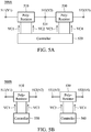
- FIG. 5A is a diagram of an impedance circuit 500A according to an embodiment of the invention.
- FIG. 5A is similar to FIG. 1 .
- the impedance circuit 500A includes a first poly-resistor 510, a second poly-resistor 530, and a controller 520.
- the first poly-resistor 510 has a first terminal 511 and a second terminal 512.
- the second poly-resistor 530 has a first terminal 531 and a second terminal 532.
- the first terminal 531 of the second poly-resistor 530 is coupled to the second terminal 512 of the first poly-resistor 510.
- the controller 520 is configured to generate a first control voltage VC1, a second control voltage VC2, a third control voltage VC3, and a fourth control voltage VC4 for controlling the first poly-resistor 510 and the second poly-resistor 530.
- the resistance between the first terminal 511 and the second terminal 512 of the first poly-resistor 510 is determined according to the first control voltage VC1 and the second control voltage VC2.
- the second control voltage VC2 is different from the first control voltage VC1.
- the resistance between the first terminal 531 and the second terminal 532 of the second poly-resistor 530 is determined according to the third control voltage VC3 and the fourth control voltage VC4.
- the fourth control voltage VC4 is different from the third control voltage VC3.
- a first poly-resistor 510 and a second poly-resistor 530 are coupled in series.
- the first control voltage VC1, the second control voltage VC2, the third control voltage VC3 and the fourth control voltage VC4 may be dynamic.
- the first control voltage VC1 and the second control voltage VC2 may be determined according to a first voltage V1 at the first terminal 511 of the first poly-resistor 510, and a second voltage V2 at the second terminal 512 of the first poly-resistor 510.
- Each of the first control voltage VC1 and the second control voltage VC2 may be a function of the first voltage V1 and the second voltage V2. The aforementioned function may be linear.
- the first control voltage VC1 may be substantially equal to the first voltage V1
- the second control voltage VC2 may be substantially equal to the second voltage V2, but they are not limited thereto.
- the third control voltage VC3 and the fourth control voltage VC4 may be determined according to the second voltage V2 at the first terminal 531 of the second poly-resistor 530, and a third voltage V3 at the second terminal 532 of the second poly-resistor 530.
- Each of the third control voltage VC3 and the fourth control voltage VC4 may be a function of the second voltage V2 and the third voltage V3. The aforementioned function may be linear.
- the third control voltage VC3 may be substantially equal to the second voltage V2
- the fourth control voltage VC4 may be substantially equal to the third voltage V3, but they are not limited thereto.
- Other features of the impedance circuit 500A of FIG. 5A are similar to those of the impedance circuit 100 of FIG. 1 . Accordingly, the two embodiments can achieve similar levels of performance.
- the impedance circuit 500A may include three or more poly-resistors which are coupled in series and controlled by the controller in a similar way although there are only two poly-resistors displayed in FIG. 5A .
- FIG. 5B is a diagram of an impedance circuit 500B according to another embodiment of the invention.
- FIG. 5B is similar to FIG. 5A .
- the impedance circuit 500B further includes a first controller 550 and a second controller 560.
- the first controller 550 is configured to generate the first control voltage VC1 and the second control voltage VC2 for controlling the first poly-resistor 510.
- the second controller 560 is configured to generate the third control voltage VC3 and the fourth control voltage VC4 for controlling the second poly-resistor 530.
- the first control voltage VC1, the second control voltage VC2, the third control voltage VC3, and the fourth control voltage VC4 may be dynamic.
- the second poly-resistor 530 is separate from the first poly-resistor 510.
- the first control voltage VC1 and the second control voltage VC2 may be determined according to a first voltage V1 at the first terminal 511 of the first poly-resistor 510, and a second voltage V2 at the second terminal 512 of the first poly-resistor 510.
- Each of the first control voltage VC1 and the second control voltage VC2 may be a function of the first voltage V1 and the second voltage V2. The aforementioned function may be linear.
- the first control voltage VC1 may be substantially equal to the first voltage V1
- the second control voltage VC2 may be substantially equal to the second voltage V2, but they are not limited thereto.
- the third control voltage VC3 and the fourth control voltage VC4 may be determined according to a third voltage V3 at the first terminal 531 of the second poly-resistor 530, and a fourth voltage V4 at the second terminal 532 of the second poly-resistor 530.
- Each of the third control voltage VC3 and the fourth control voltage VC4 may be a function of the third voltage V3 and the fourth voltage V4. The aforementioned function may be linear.
- the third control voltage VC3 may be substantially equal to the third voltage V3, and the fourth control voltage VC4 may be substantially equal to the fourth voltage V4, but they are not limited thereto.
- Other features of the impedance circuit 500B of FIG. 5B are similar to those of the impedance circuit 500A of FIG. 5A . It should be noted that the impedance circuit 500B may include three or even more poly-resistors which are respectively controlled by three or more controllers in a similar way.
- the proposed impedance circuit and the poly-resistor therein can be applied to a variety of circuits. Please refer to the following embodiments in FIGS. 6-8 .
- FIG. 6A is a diagram of a differential or pseudo-differential amplifier 600A according to an embodiment of the invention.
- the differential or pseudo-differential amplifier 600A generates a positive output voltage VOP and a negative output voltage VON according to a positive input voltage VIP and a negative input voltage VIN.
- the differential or pseudo-differential amplifier 600A includes a main operational amplifier 610, an auxiliary operational amplifier 620, a first resistor R1, a second resistor R2, a third resistor R3, a fourth resistor R4, a controller 520, a first poly-resistor 510, and a second poly-resistor 530.
- the first resistor R1 is coupled between the negative input voltage VIN and a negative input terminal of the main operational amplifier 610.
- the second resistor R2 is coupled between the positive input voltage VIP and a positive input terminal of the main operational amplifier 610.
- the third resistor R3 is coupled between the negative input terminal and a positive output terminal (i.e., the positive output voltage VOP) of the main operational amplifier 610.
- the fourth resistor R4 is coupled between the positive input terminal and a negative output terminal (i.e., the negative output voltage VON) of the main operational amplifier 610.
- An inner voltage VAV is between the first poly-resistor 510 and the second resistor 530, and it may be close to a common voltage VCM.
- the first poly-resistor 510 is coupled between the positive output terminal (i.e., the positive output voltage VOP) of the main operational amplifier 610 and the inner voltage VAV.
- the second poly-resistor 530 is coupled between the inner voltage VAV and the negative output terminal (i.e., the negative output voltage VON) of the main operational amplifier 610.
- the auxiliary operational amplifier 620 compares the inner voltage VAV with the common voltage VCM, so as to adjust a DC (Direct Current) offset of the main operational amplifier 610 with a negative feedback mechanism.
- the common voltage VCM may be set to a ground voltage VSS (e.g., 0V).
- the controller 520 is configured to generate a first control voltage VC1 and a second control voltage VC2 for controlling the first poly-resistor 510, and further generate a third control voltage VC3 and a fourth control voltage VC4 for controlling the second poly-resistor 530.
- the first control voltage VC1, the second control voltage VC2, the third control voltage VC3, and the fourth control voltage VC4 are determined according to the positive output voltage VOP, the negative output voltage VON, and the inner voltage VAV.
- each of the first control signal VC1 and the second control signal VC2 may be dynamic and be a function of the positive output voltage VOP and the inner voltage VAV; and each of the third control signal VC3 and the fourth control signal VC4 may be dynamic and be a function of the inner voltage VAV and the negative output voltage VON.
- the first control voltage VC1 may be substantially equal to the positive output voltage VOP
- the second control voltage VC2 and the third control voltage VC3 may be both substantially equal to the inner voltage VAV
- the fourth control voltage VC4 may be substantially equal to the negative output voltage VON, but they are not limited thereto.
- each of the first poly-resistor 510 and the second poly-resistor 530 is a common-mode feedback resistor used in the differential or pseudo-differential amplifier 600A.
- FIG. 6B is a diagram of a differential or pseudo-differential amplifier 600B according to an embodiment of the invention.
- FIG. 6B is similar to FIG. 6A .
- the controller 520 controls the first poly-resistor 510 and the second resistor 530 according to the positive input voltage VIP and the negative input voltage VIN, which are related to the positive output voltage VOP and the negative output voltage VON.
- FIG. 6C is a diagram of a differential or pseudo-differential amplifier 600C according to an embodiment of the invention.
- FIG. 6C is similar to FIG. 6A .
- FIG. 6A In the embodiment of FIG.
- FIG. 6C is a diagram of a differential or pseudo-differential amplifier 600D according to an embodiment of the invention.
- FIG. 6D is similar to FIG. 6C .
- the controller 520 controls the first poly-resistor 510 and the second resistor 530 according to the positive input current IIP and the negative input current IIN, which are related to the positive output voltage VOP and the negative output voltage VON.
- Other features of the differential or pseudo-differential amplifiers 600B, 600C, and 600D of FIGS. 6B , 6C, and 6D are similar to those of the differential or pseudo-differential amplifier 600A of FIG. 6A . Accordingly, these embodiments can achieve similar levels of performance.
- FIG. 7A is a diagram of a differential-to-single-ended amplifier 700A according to an embodiment of the invention.
- the differential-to-single-ended amplifier 700A generates a positive output voltage VOP according to a positive input voltage VIP and a negative input voltage VIN.
- the differential-to-single-ended amplifier 700A includes a main operational amplifier 610, a first resistor R1, a second resistor R2, a first poly-resistor 510, a second poly-resistor 530, a first controller 550, and a second controller 560.
- the first resistor R1 is coupled between the negative input voltage VIN and a negative input terminal of the main operational amplifier 610.
- the second resistor R2 is coupled between the positive input voltage VIP and a positive input terminal of the main operational amplifier 610.
- a positive inner voltage VIPX is at the positive input terminal of the main operational amplifier 610.
- the first poly-resistor 510 is coupled between the negative input terminal and a positive output terminal (i.e., the positive output voltage VOP) of the main operational amplifier 610.
- the second poly-resistor 530 is coupled between the positive input terminal of the main operational amplifier 610 and a ground voltage VSS.
- the first controller 550 is configured to generate a first control voltage VC1 and a second control voltage VC2 for controlling the first poly-resistor 510.
- the second controller 560 is configured to generate a third control voltage VC3 and a fourth control voltage VC4 for controlling the second poly-resistor 530.
- the first control voltage VC1, the second control voltage VC2, the third control voltage VC3, and the fourth control voltage VC4 are determined according to the positive output voltage VOP, the positive inner voltage VIPX, and the ground voltage VSS.
- each of the first control signal VC1 and the second control signal VC2 may be dynamic and be a function of the positive inner voltage VIPX and the positive output voltage VOP; and each of the third control signal VC3 and the fourth control signal VC4 may be dynamic and be a function of the positive inner voltage VIPX and the ground voltage VSS.
- first control voltage VC1 and the third control voltage VC3 may be substantially equal to the positive inner voltage VIPX
- the second control voltage VC2 may be substantially equal to the positive output voltage VOP
- the fourth control voltage VC4 may be substantially equal to the ground voltage VSS, but they are not limited thereto.
- each of the first poly-resistor 510 and the second poly-resistor 530 is a feedback resistor used in the differential-to-single-ended amplifier 700A.
- FIG. 7B is a diagram of a differential-to-single-ended amplifier 700B according to an embodiment of the invention.
- FIG. 7B is similar to FIG. 7A .
- the first controller 550 controls the first poly-resistor 510 according to the positive input voltage VIP, which is related to the positive output voltage VOP.
- FIG. 7C is a diagram of a differential-to-single-ended amplifier 700C according to an embodiment of the invention.
- FIG. 7C is similar to FIG. 7A .
- the differential-to-single-ended amplifier 700C generates the positive output voltage VOP according to a positive input current IIP and a negative input current IIN FIG.
- FIG. 7D is a diagram of a differential-to-single-ended amplifier 700D according to an embodiment of the invention.
- FIG. 7D is similar to FIG. 7C .
- the first controller 550 controls the first poly-resistor 510 according to the positive input current IIP, which is related to the positive output voltage VOP.
- Other features of the differential-to-single-ended amplifiers 700B, 700C, and 700D of FIGS. 7B , 7C, and 7D are similar to those of the differential-to-single-ended amplifier 700A of FIG. 7A . Accordingly, these embodiments can achieve similar levels of performance.
- FIG. 8A is a diagram of an inverting amplifier 800A according to an embodiment of the invention.
- the inverting amplifier 800A generates a positive output voltage VOP according to a negative input voltage VIN.
- the inverting amplifier 800A includes a main operational amplifier 610, a first resistor R1, a controller 120, and a poly-resistor 110.
- the first resistor R1 is coupled between the negative input voltage VIN and a negative input terminal of the main operational amplifier 610.
- a common voltage VCM is at a positive input terminal of the main operational amplifier 610.
- the common voltage VCM may be set to a ground voltage VSS (e.g., 0V).
- the poly-resistor 110 is coupled between the negative input terminal and a positive output terminal (i.e., the positive output voltage VOP) of the main operational amplifier 610.
- the controller 120 is configured to generate a first control voltage VC1 and a second control voltage VC2 for controlling the poly-resistor 110.
- the first control voltage VC1 and the second control voltage VC2 are determined according to the positive output voltage VOP and the common voltage VCM.
- each of the first control signal VC1 and the second control signal VC2 may be dynamic and be a function of the positive output voltage VOP and the common voltage VCM.
- the first control voltage VC1 may be substantially equal to the common voltage VCM, and the second control voltage VC2 may be substantially equal to the positive output voltage VOP, but they are not limited thereto.
- the poly-resistor 110 is a feedback resistor used in the inverting amplifier 800A.
- FIG. 8B is a diagram of an inverting amplifier 800B according to an embodiment of the invention.
- FIG. 8B is similar to FIG. 8A .
- the inverting amplifier 800B generates the positive output voltage VOP according to a negative input current IIN.
- FIG. 8C is a diagram of an inverting amplifier 800C according to an embodiment of the invention.
- FIG. 8C is similar to FIG. 8B .
- the controller 120 controls the poly-resistor 110 according to the positive input current IIN, which is related to the positive output voltage VOP.
- Other features of the inverting amplifiers 800B and 800C of FIGS. 8B and FIG. 8C are similar to those of the inverting amplifier 800A of FIG. 8A . Accordingly, these embodiments can achieve similar levels of performance.
- the invention proposes a novel impedance circuit including a poly-resistor and a controller.
- the proposed controller can compensate for non-linearity of the poly-resistor.
- the poly-resistor may be further divided into a plurality of sub-poly-resistors coupled in series, without affecting the performance of the proposed impedance circuit.
- the proposed impedance circuit can eliminate the depletion effect of the poly-resistor, and make the poly-resistor be more linear and subject to Ohm's law.
- the impedance circuit and poly-resistor of the invention are not limited to the configurations of FIGS. 1-8 .
- the invention may merely include any one or more features of any one or more embodiments of FIGS. 1-8 . In other words, not all of the features displayed in the figures should be implemented in the impedance circuit and poly-resistor of the invention.
Landscapes
- Engineering & Computer Science (AREA)
- Power Engineering (AREA)
- Physics & Mathematics (AREA)
- Nonlinear Science (AREA)
- Amplifiers (AREA)
- Networks Using Active Elements (AREA)
Abstract
Description
- The disclosure generally relates to an impedance circuit, and more specifically, to an impedance circuit and a poly-resistor therein.
- Poly-resistors are characterized by their sheet resistance values. In order to reduce the chip size, the poly-resistors with high sheet resistance values are often used and fabricated in a small area, and they are extensively used in a variety of integrated circuits.
- However, the depletion effect is a phenomenon in which there is unwanted variation in the threshold voltage of devices using poly-silicon as a gate material, leading to unpredictable behavior on the part of electronic circuits. It results in serious non-linearity of the poly-resistors. Accordingly, there is a need for a novel solution for suppressing the non-ideal depletion effect in poly-resistors.
- In a preferred embodiment, the disclosure is directed to an impedance circuit including a poly-resistor and a controller. The poly-resistor has a first terminal and a second terminal. The controller generates a first control voltage and a second control voltage. The resistance between the first terminal and the second terminal of the poly-resistor is determined according to the first control voltage and the second control voltage. The second control voltage is different from the first control voltage. The proposed impedance circuit can improve the linearity of the poly-resistor.
- In some embodiments, the poly-resistor includes a poly-silicon layer, a channel layer, and an insulation layer. The poly-silicon layer has a first end and a second end. The first end of the poly-silicon layer is coupled to the first terminal of the poly-resistor, and the second end of the poly-silicon layer is coupled to the second terminal of the poly-resistor. The channel layer has a first end and a second end. The first end of the channel layer is arranged for receiving the first control voltage, and the second end of the channel layer is arranged for receiving the second control voltage. The insulation layer is disposed between the poly-silicon layer and the channel layer.
- In some embodiments, the first end of the channel layer is close to the first end of the poly-silicon layer, and the second end of the channel layer is close to the second end of the poly-silicon layer.
- In some embodiments, the channel layer is a conductive layer, a semiconductor layer, or another poly-silicon layer.
- In some embodiments, the channel layer is an n-well, and the first end and the second end of the channel layer are n+ doped regions.
- In some embodiments, the channel layer is a p-well, and the first end and the second end of the channel layer are p+ doped regions.
- In some embodiments, the insulation layer is made of different materials, such as a silicon dioxide layer, a field oxide (FOX) layer, or shallow trench isolation (STI) layer.
- In some embodiments, the first control voltage and the second control voltage are dynamic.
- In some embodiments, the first control voltage and the second control voltage are determined according to a first voltage at the first terminal of the poly-resistor, and a second voltage at the second terminal of the poly-resistor.
- In some embodiments, each of the first control voltage and the second control voltage is a linear function of the first voltage and the second voltage.
- In some embodiments, the first control voltage is substantially equal to the first voltage, and the second control voltage is substantially equal to the second voltage.
- In some embodiments, the poly-resistor is a feedback resistor.
- In some embodiments, the poly-resistor is a common-mode feedback resistor.
- In some embodiments, the poly-resistor is used in a differential or pseudo-differential amplifier.
- In some embodiments, the poly-resistor is used in a differential-to-single-ended amplifier.
- In some embodiments, the poly-resistor is used in an inverting amplifier.
- In some embodiments, the poly-resistor comprises a plurality of sub-poly-resistors coupled in series.
- The invention can be more fully understood by reading the subsequent detailed description and examples with references made to the accompanying drawings, wherein:
-
FIG. 1 is a diagram of an impedance circuit according to an embodiment of the invention; -
FIG. 2 is a diagram of a poly-resistor according to an embodiment of the invention; -
FIG. 3 is a diagram of a poly-resistor according to an embodiment of the invention; -
FIG. 4 is a diagram of a poly-resistor according to an embodiment of the invention; -
FIG. 5A is a diagram of an impedance circuit according to an embodiment of the invention; -
FIG. 5B is a diagram of an impedance circuit according to another embodiment of the invention; -
FIG. 6A is a diagram of a differential or pseudo-differential amplifier according to an embodiment of the invention; -
FIG. 6B is a diagram of a differential or pseudo-differential amplifier according to an embodiment of the invention; -
FIG. 6C is a diagram of a differential or pseudo-differential amplifier according to an embodiment of the invention; -
FIG. 6D is a diagram of a differential or pseudo-differential amplifier according to an embodiment of the invention; -
FIG. 7A is a diagram of a differential-to-single-ended amplifier according to an embodiment of the invention; -
FIG. 7B is a diagram of a differential-to-single-ended amplifier according to an embodiment of the invention; -
FIG. 7C is a diagram of a differential-to-single-ended amplifier according to an embodiment of the invention; -
FIG. 7D is a diagram of a differential-to-single-ended amplifier according to an embodiment of the invention; -
FIG. 8A is a diagram of an inverting amplifier according to an embodiment of the invention; -
FIG. 8B is a diagram of an inverting amplifier according to an embodiment of the invention; and -
FIG. 8C is a diagram of an inverting amplifier according to an embodiment of the invention. - In order to illustrate the purposes, features and advantages of the invention, the embodiments and figures of the invention will be described in detail as follows.
- Certain terms are used throughout the description and following claims to refer to particular components. As one skilled in the art will appreciate, manufacturers may refer to a component by different names. This document does not intend to distinguish between components that differ in name but not function. In the following description and in the claims, the terms "include" and "comprise" are used in an open-ended fashion, and thus should be interpreted to mean "include, but not limited to...". The term "substantially" means the value is within an acceptable error range. One skilled in the art can solve the technical problem within a predetermined error range and achieve the proposed technical performance. Also, the term "couple" is intended to mean either an indirect or direct electrical connection. Accordingly, if one device is coupled to another device, that connection may be through a direct electrical connection, or through an indirect electrical connection via other devices and connections.
-
FIG. 1 is a diagram of animpedance circuit 100 according to an embodiment of the invention. Theimpedance circuit 100 includes a poly-resistor 110 and acontroller 120. The poly-resistor 110 has afirst terminal 111 and asecond terminal 112. If a second voltage V2 at thesecond terminal 112 is higher than a first voltage V1 at the first terminal 111 (i.e., a driving voltage difference (V2-V1) is applied to the poly-resistor 110), a current through the poly-resistor 110 will flow from thesecond terminal 112 to thefirst terminal 111. Thecontroller 120 may be a voltage generator, a voltage divider, or a weighted summer circuit. Thecontroller 120 is configured to generate a first control voltage VC1 and a second control voltage VC2 for controlling the poly-resistor 110. The resistance between thefirst terminal 111 and thesecond terminal 112 of the poly-resistor 110 is determined according to the first control voltage VC1 and the second control voltage VC2.In one embodiment, the second control voltage VC2 is different from the first control voltage VC1. - Such a design can improve the linearity of the poly-
resistor 110. Please refer to the following embodiments and figures. It should be noted that these embodiments and figures are exemplary, rather than restricted limitations of the invention. -
FIG. 2 is a diagram of a poly-resistor 210 according to an embodiment of the invention.FIG. 2 illustrates the detailed physical structure of the poly-resistor 110 ofFIG. 1 . InFIG. 2 , the poly-resistor 210 with afirst terminal 211 and asecond terminal 212 includes a poly-silicon layer 220, achannel layer 230 and aninsulation layer 240. The poly-silicon layer 220 has afirst end 221 and asecond end 222, which are located apart from each other. Thefirst end 221 of the poly-silicon layer 220 is coupled to thefirst terminal 211 of the poly-resistor 210, and thesecond end 222 of the poly-silicon layer 220 is coupled to thesecond terminal 212 of the poly-resistor 210. If a second voltage V2 at thesecond terminal 212 is higher than a first voltage V1 at the first terminal 211 (i.e., a driving voltage difference (V2-VI) is applied to the poly-resistor 210), a current through the poly-resistor 210 will flow from thesecond terminal 212 to thefirst terminal 211. That is, the current may flow through the poly-silicon layer 220, from thesecond end 222 to thefirst end 221. Thechannel layer 230 may be a conductive layer, a semiconductor layer, or another poly-silicon layer which is different from the poly-silicon layer 220. Thechannel layer 230 has a first end 231 and asecond end 232, which are located apart from each other. The first end 231 of thechannel layer 230 is arranged for receiving the first control voltage VC1, and thesecond end 232 of thechannel layer 230 is arranged for receiving the second control voltage VC2. In some embodiments, the first end 231 of thechannel layer 230 is closer to thefirst end 221 of the poly-silicon layer 220 than to thesecond end 232 of thechannel layer 230, and thesecond end 232 of thechannel layer 230 is closer to thesecond end 222 of the poly-silicon layer 220 than to the first end 231 of thechannel layer 230. As a result, the first control voltage VC1 controls the operation characteristic (e.g., the resistance) of thefirst end 221 of the poly-silicon layer 220, and the second control voltage VC2 controls the operation characteristic (e.g., the resistance) of thesecond end 222 of the poly-silicon layer 220. Theinsulation layer 240 may be made of any nonconductive material. Theinsulation layer 240 is disposed between the poly-silicon layer 220 and thechannel layer 230, and is configured to isolate the poly-silicon layer 220 from thechannel layer 230. - Please refer to
FIG. 1 further in view ofFIG. 2 and understand the operation theory of the invention. To suppress the depletion effect of the poly-resistor 110, the first control voltage VC1 and the second control voltage VC2 may be dynamic, instead of being constant values. For example, the first control voltage VC1 and the second control voltage VC2 may be determined according to the first voltage V1 at thefirst terminal 111 of the poly-resistor 110, and the second voltage V2 at thesecond terminal 112 of the poly-resistor 110. That is, each of the first control voltage VC1 and the second control voltage VC2 may be a function of the first voltage V1 and the second voltage V2. The aforementioned functions may be linear and expressed as the following equations (1) to (3):


- The above values A, B, C, and D are adjustable in response to different requirements. Specifically, when the
controller 120 dynamically adjusts the first control voltage VC1 and the second control voltage VC2 in response to the first voltage V1 and the second voltage V2, the depletion effect of the poly-resistor 110 can be suppressed. The proposed impedance circuit is more linear and more concentrated than the conventional poly-resistor in which only one control voltage is applied to the poly-resistor, or the control voltage applied to the poly-resistor is fixed. - In some embodiments, the first control voltage VC1 is substantially equal to the first voltage V1, and the second control voltage VC2 is substantially equal to the second voltage V2. That is, according to the equations (1) to (3), the values A and D are both set to 1, and the values B and C are both set to 0. Please refer to the physical structure of
FIG. 2 . If the first control voltage VC1 is equal to the first voltage V1 and the second control voltage VC2 is equal to the second voltage V2, the control voltage difference (e.g., VC2-VC1) between the second control voltage VC2 and the first control voltage VC1 will be the same as the driving voltage difference (e.g.,V2-V1) between thesecond terminal 212 and thefirst terminal 211 of the poly-resistor 210. The control voltage difference (e.g., VC2-VC1) is uniformly distributed over thechannel layer 230, and it is consistent with the driving voltage difference (e.g.,V2-V1) which is uniformly distributed over the poly-silicon layer 220. With such a design, thechannel layer 230 has almost the same voltage level distribution as that of the poly-silicon layer 220, and no effective voltage difference exists between thechannel layer 230 and the poly-silicon layer 220. Therefore, compared with the conventional method applying only one control voltage, the depletion effect of the poly-resistor 210 can be eliminated, and the poly-resistor 210 can provide resistance to accomplish better and more concentrated linearity. -
FIG. 3 is a diagram of a poly-resistor 310 according to an embodiment of the invention.FIG. 3 is similar toFIG. 2 . In the embodiment ofFIG. 3 , achannel layer 330 of the poly-resistor 310 is an N-type doped layer, which may be configured in a P-type dopedlayer 350, and a first end 331 and asecond end 332 of thechannel layer 330 are n+ doped regions. Aninsulation layer 340 of the poly-resistor 310 can be of different materials, such as a silicon dioxide layer, a field oxide (FOX) layer, or a Shallow Trench Isolation (STI) layer, but is not limited thereto. Other features of the poly-resistor 310 ofFIG. 3 are similar to those of the poly-resistor 210 ofFIG. 2 .FIG. 4 is a diagram of a poly-resistor 410 according to an embodiment of the invention.FIG. 4 is similar toFIG. 2 . In the embodiment ofFIG. 4 , achannel layer 430 of the poly-resistor 410 is a P-type doped layer, which may be configured in an N-type dopedlayer 450, and a first end 431 and asecond end 432 of thechannel layer 430 are p+ doped regions. Aninsulation layer 440 can be of different materials, such as a silicon dioxide layer, a field oxide (FOX) layer, or a STI layer, but is not limited thereto. Other features of the poly-resistor 410 ofFIG. 4 are similar to those of the poly-resistor 210 ofFIG. 2 . -
FIG. 5A is a diagram of animpedance circuit 500A according to an embodiment of the invention.FIG. 5A is similar toFIG. 1 . In the embodiment ofFIG. 5A , theimpedance circuit 500A includes a first poly-resistor 510, a second poly-resistor 530, and acontroller 520. The first poly-resistor 510 has afirst terminal 511 and asecond terminal 512. The second poly-resistor 530 has afirst terminal 531 and asecond terminal 532. Thefirst terminal 531 of the second poly-resistor 530 is coupled to thesecond terminal 512 of the first poly-resistor 510. Thecontroller 520 is configured to generate a first control voltage VC1, a second control voltage VC2, a third control voltage VC3, and a fourth control voltage VC4 for controlling the first poly-resistor 510 and the second poly-resistor 530. The resistance between thefirst terminal 511 and thesecond terminal 512 of the first poly-resistor 510 is determined according to the first control voltage VC1 and the second control voltage VC2. In one embodiment, the second control voltage VC2 is different from the first control voltage VC1. The resistance between thefirst terminal 531 and thesecond terminal 532 of the second poly-resistor 530 is determined according to the third control voltage VC3 and the fourth control voltage VC4. In one embodiment, the fourth control voltage VC4 is different from the third control voltage VC3. - In the
impedance circuit 500A, a first poly-resistor 510 and a second poly-resistor 530 are coupled in series. The first control voltage VC1, the second control voltage VC2, the third control voltage VC3 and the fourth control voltage VC4 may be dynamic. The first control voltage VC1 and the second control voltage VC2 may be determined according to a first voltage V1 at thefirst terminal 511 of the first poly-resistor 510, and a second voltage V2 at thesecond terminal 512 of the first poly-resistor 510. Each of the first control voltage VC1 and the second control voltage VC2 may be a function of the first voltage V1 and the second voltage V2. The aforementioned function may be linear. For example, the first control voltage VC1 may be substantially equal to the first voltage V1, and the second control voltage VC2 may be substantially equal to the second voltage V2, but they are not limited thereto. The third control voltage VC3 and the fourth control voltage VC4 may be determined according to the second voltage V2 at thefirst terminal 531 of the second poly-resistor 530, and a third voltage V3 at thesecond terminal 532 of the second poly-resistor 530. Each of the third control voltage VC3 and the fourth control voltage VC4 may be a function of the second voltage V2 and the third voltage V3. The aforementioned function may be linear. For example, the third control voltage VC3 may be substantially equal to the second voltage V2, and the fourth control voltage VC4 may be substantially equal to the third voltage V3, but they are not limited thereto. Other features of theimpedance circuit 500A ofFIG. 5A are similar to those of theimpedance circuit 100 ofFIG. 1 . Accordingly, the two embodiments can achieve similar levels of performance. It should be noted that theimpedance circuit 500A may include three or more poly-resistors which are coupled in series and controlled by the controller in a similar way although there are only two poly-resistors displayed inFIG. 5A . -
FIG. 5B is a diagram of animpedance circuit 500B according to another embodiment of the invention.FIG. 5B is similar toFIG. 5A . In the embodiment ofFIG. 5B , theimpedance circuit 500B further includes afirst controller 550 and asecond controller 560. Such a design can also suppress the non-linear depletion effect. Thefirst controller 550 is configured to generate the first control voltage VC1 and the second control voltage VC2 for controlling the first poly-resistor 510. Thesecond controller 560 is configured to generate the third control voltage VC3 and the fourth control voltage VC4 for controlling the second poly-resistor 530. Similarly, the first control voltage VC1, the second control voltage VC2, the third control voltage VC3, and the fourth control voltage VC4 may be dynamic. In theimpedance circuit 500B, the second poly-resistor 530 is separate from the first poly-resistor 510. The first control voltage VC1 and the second control voltage VC2 may be determined according to a first voltage V1 at thefirst terminal 511 of the first poly-resistor 510, and a second voltage V2 at thesecond terminal 512 of the first poly-resistor 510. Each of the first control voltage VC1 and the second control voltage VC2 may be a function of the first voltage V1 and the second voltage V2. The aforementioned function may be linear. For example, the first control voltage VC1 may be substantially equal to the first voltage V1, and the second control voltage VC2 may be substantially equal to the second voltage V2, but they are not limited thereto. The third control voltage VC3 and the fourth control voltage VC4 may be determined according to a third voltage V3 at thefirst terminal 531 of the second poly-resistor 530, and a fourth voltage V4 at thesecond terminal 532 of the second poly-resistor 530. Each of the third control voltage VC3 and the fourth control voltage VC4 may be a function of the third voltage V3 and the fourth voltage V4. The aforementioned function may be linear. For example, the third control voltage VC3 may be substantially equal to the third voltage V3, and the fourth control voltage VC4 may be substantially equal to the fourth voltage V4, but they are not limited thereto. Other features of theimpedance circuit 500B ofFIG. 5B are similar to those of theimpedance circuit 500A ofFIG. 5A . It should be noted that theimpedance circuit 500B may include three or even more poly-resistors which are respectively controlled by three or more controllers in a similar way. - The proposed impedance circuit and the poly-resistor therein can be applied to a variety of circuits. Please refer to the following embodiments in
FIGS. 6-8 . -
FIG. 6A is a diagram of a differential orpseudo-differential amplifier 600A according to an embodiment of the invention. In the embodiment ofFIG. 6A , the differential orpseudo-differential amplifier 600A generates a positive output voltage VOP and a negative output voltage VON according to a positive input voltage VIP and a negative input voltage VIN. Specifically, the differential orpseudo-differential amplifier 600A includes a mainoperational amplifier 610, an auxiliaryoperational amplifier 620, a first resistor R1, a second resistor R2, a third resistor R3, a fourth resistor R4, acontroller 520, a first poly-resistor 510, and a second poly-resistor 530. The first resistor R1 is coupled between the negative input voltage VIN and a negative input terminal of the mainoperational amplifier 610. The second resistor R2 is coupled between the positive input voltage VIP and a positive input terminal of the mainoperational amplifier 610. The third resistor R3 is coupled between the negative input terminal and a positive output terminal (i.e., the positive output voltage VOP) of the mainoperational amplifier 610. The fourth resistor R4 is coupled between the positive input terminal and a negative output terminal (i.e., the negative output voltage VON) of the mainoperational amplifier 610. An inner voltage VAV is between the first poly-resistor 510 and thesecond resistor 530, and it may be close to a common voltage VCM. The first poly-resistor 510 is coupled between the positive output terminal (i.e., the positive output voltage VOP) of the mainoperational amplifier 610 and the inner voltage VAV. The second poly-resistor 530 is coupled between the inner voltage VAV and the negative output terminal (i.e., the negative output voltage VON) of the mainoperational amplifier 610. The auxiliaryoperational amplifier 620 compares the inner voltage VAV with the common voltage VCM, so as to adjust a DC (Direct Current) offset of the mainoperational amplifier 610 with a negative feedback mechanism. The common voltage VCM may be set to a ground voltage VSS (e.g., 0V). Thecontroller 520 is configured to generate a first control voltage VC1 and a second control voltage VC2 for controlling the first poly-resistor 510, and further generate a third control voltage VC3 and a fourth control voltage VC4 for controlling the second poly-resistor 530. In some embodiments, the first control voltage VC1, the second control voltage VC2, the third control voltage VC3, and the fourth control voltage VC4 are determined according to the positive output voltage VOP, the negative output voltage VON, and the inner voltage VAV. Specifically, each of the first control signal VC1 and the second control signal VC2 may be dynamic and be a function of the positive output voltage VOP and the inner voltage VAV; and each of the third control signal VC3 and the fourth control signal VC4 may be dynamic and be a function of the inner voltage VAV and the negative output voltage VON. For example, the first control voltage VC1 may be substantially equal to the positive output voltage VOP, the second control voltage VC2 and the third control voltage VC3 may be both substantially equal to the inner voltage VAV, and the fourth control voltage VC4 may be substantially equal to the negative output voltage VON, but they are not limited thereto. In the embodiment ofFIG. 6A , each of the first poly-resistor 510 and the second poly-resistor 530 is a common-mode feedback resistor used in the differential orpseudo-differential amplifier 600A. -
FIG. 6B is a diagram of a differential orpseudo-differential amplifier 600B according to an embodiment of the invention.FIG. 6B is similar toFIG. 6A . In the embodiment ofFIG. 6B , thecontroller 520 controls the first poly-resistor 510 and thesecond resistor 530 according to the positive input voltage VIP and the negative input voltage VIN, which are related to the positive output voltage VOP and the negative output voltage VON.FIG. 6C is a diagram of a differential orpseudo-differential amplifier 600C according to an embodiment of the invention.FIG. 6C is similar toFIG. 6A . In the embodiment ofFIG. 6C , the differential orpseudo-differential amplifier 600C generates the positive output voltage VOP and the negative output voltage VON according to a positive input current IIP and a negative input current IIN.FIG. 6D is a diagram of a differential orpseudo-differential amplifier 600D according to an embodiment of the invention.FIG. 6D is similar toFIG. 6C . In the embodiment ofFIG. 6D , thecontroller 520 controls the first poly-resistor 510 and thesecond resistor 530 according to the positive input current IIP and the negative input current IIN, which are related to the positive output voltage VOP and the negative output voltage VON. Other features of the differential orpseudo-differential amplifiers FIGS. 6B ,6C, and 6D are similar to those of the differential orpseudo-differential amplifier 600A ofFIG. 6A . Accordingly, these embodiments can achieve similar levels of performance. -
FIG. 7A is a diagram of a differential-to-single-endedamplifier 700A according to an embodiment of the invention. In the embodiment ofFIG. 7A , the differential-to-single-endedamplifier 700A generates a positive output voltage VOP according to a positive input voltage VIP and a negative input voltage VIN. Specifically, the differential-to-single-endedamplifier 700A includes a mainoperational amplifier 610, a first resistor R1, a second resistor R2, a first poly-resistor 510, a second poly-resistor 530, afirst controller 550, and asecond controller 560. The first resistor R1 is coupled between the negative input voltage VIN and a negative input terminal of the mainoperational amplifier 610. The second resistor R2 is coupled between the positive input voltage VIP and a positive input terminal of the mainoperational amplifier 610. A positive inner voltage VIPX is at the positive input terminal of the mainoperational amplifier 610. The first poly-resistor 510 is coupled between the negative input terminal and a positive output terminal (i.e., the positive output voltage VOP) of the mainoperational amplifier 610. The second poly-resistor 530 is coupled between the positive input terminal of the mainoperational amplifier 610 and a ground voltage VSS. Thefirst controller 550 is configured to generate a first control voltage VC1 and a second control voltage VC2 for controlling the first poly-resistor 510. Thesecond controller 560 is configured to generate a third control voltage VC3 and a fourth control voltage VC4 for controlling the second poly-resistor 530. In some embodiments, the first control voltage VC1, the second control voltage VC2, the third control voltage VC3, and the fourth control voltage VC4 are determined according to the positive output voltage VOP, the positive inner voltage VIPX, and the ground voltage VSS. Specifically, each of the first control signal VC1 and the second control signal VC2 may be dynamic and be a function of the positive inner voltage VIPX and the positive output voltage VOP; and each of the third control signal VC3 and the fourth control signal VC4 may be dynamic and be a function of the positive inner voltage VIPX and the ground voltage VSS. For example, the first control voltage VC1 and the third control voltage VC3 may be substantially equal to the positive inner voltage VIPX, the second control voltage VC2 may be substantially equal to the positive output voltage VOP, and the fourth control voltage VC4 may be substantially equal to the ground voltage VSS, but they are not limited thereto. In the embodiment ofFIG. 7A , each of the first poly-resistor 510 and the second poly-resistor 530 is a feedback resistor used in the differential-to-single-endedamplifier 700A. -
FIG. 7B is a diagram of a differential-to-single-endedamplifier 700B according to an embodiment of the invention.FIG. 7B is similar toFIG. 7A . In the embodiment ofFIG. 7B , thefirst controller 550 controls the first poly-resistor 510 according to the positive input voltage VIP, which is related to the positive output voltage VOP.FIG. 7C is a diagram of a differential-to-single-endedamplifier 700C according to an embodiment of the invention.FIG. 7C is similar toFIG. 7A . In the embodiment ofFIG. 7C , the differential-to-single-endedamplifier 700C generates the positive output voltage VOP according to a positive input current IIP and a negative input current IINFIG. 7D is a diagram of a differential-to-single-endedamplifier 700D according to an embodiment of the invention.FIG. 7D is similar toFIG. 7C . In the embodiment ofFIG. 7D , thefirst controller 550 controls the first poly-resistor 510 according to the positive input current IIP, which is related to the positive output voltage VOP. Other features of the differential-to-single-endedamplifiers FIGS. 7B ,7C, and 7D are similar to those of the differential-to-single-endedamplifier 700A ofFIG. 7A . Accordingly, these embodiments can achieve similar levels of performance. -
FIG. 8A is a diagram of an invertingamplifier 800A according to an embodiment of the invention. In the embodiment ofFIG. 8A , the invertingamplifier 800A generates a positive output voltage VOP according to a negative input voltage VIN. Specifically, the invertingamplifier 800A includes a mainoperational amplifier 610, a first resistor R1, acontroller 120, and a poly-resistor 110. The first resistor R1 is coupled between the negative input voltage VIN and a negative input terminal of the mainoperational amplifier 610. A common voltage VCM is at a positive input terminal of the mainoperational amplifier 610. The common voltage VCM may be set to a ground voltage VSS (e.g., 0V). The poly-resistor 110 is coupled between the negative input terminal and a positive output terminal (i.e., the positive output voltage VOP) of the mainoperational amplifier 610. Thecontroller 120 is configured to generate a first control voltage VC1 and a second control voltage VC2 for controlling the poly-resistor 110. In some embodiments, the first control voltage VC1 and the second control voltage VC2 are determined according to the positive output voltage VOP and the common voltage VCM. Specifically, each of the first control signal VC1 and the second control signal VC2 may be dynamic and be a function of the positive output voltage VOP and the common voltage VCM. For example, the first control voltage VC1 may be substantially equal to the common voltage VCM, and the second control voltage VC2 may be substantially equal to the positive output voltage VOP, but they are not limited thereto. In the embodiment ofFIG. 8A , the poly-resistor 110 is a feedback resistor used in the invertingamplifier 800A. -
FIG. 8B is a diagram of an invertingamplifier 800B according to an embodiment of the invention.FIG. 8B is similar toFIG. 8A . In the embodiment ofFIG. 8B , the invertingamplifier 800B generates the positive output voltage VOP according to a negative input current IIN.FIG. 8C is a diagram of an invertingamplifier 800C according to an embodiment of the invention.FIG. 8C is similar toFIG. 8B . In the embodiment ofFIG. 8C , thecontroller 120 controls the poly-resistor 110 according to the positive input current IIN, which is related to the positive output voltage VOP. Other features of the invertingamplifiers FIGS. 8B andFIG. 8C are similar to those of the invertingamplifier 800A ofFIG. 8A . Accordingly, these embodiments can achieve similar levels of performance. - The invention proposes a novel impedance circuit including a poly-resistor and a controller. The proposed controller can compensate for non-linearity of the poly-resistor. Alternatively, the poly-resistor may be further divided into a plurality of sub-poly-resistors coupled in series, without affecting the performance of the proposed impedance circuit. To be brief, the proposed impedance circuit can eliminate the depletion effect of the poly-resistor, and make the poly-resistor be more linear and subject to Ohm's law.
- Note that the above voltages, currents, resistances, inductances, capacitances and other element parameters are not limitations of the invention. A designer can adjust these parameters according to different requirements. The impedance circuit and poly-resistor of the invention are not limited to the configurations of
FIGS. 1-8 . The invention may merely include any one or more features of any one or more embodiments ofFIGS. 1-8 . In other words, not all of the features displayed in the figures should be implemented in the impedance circuit and poly-resistor of the invention. - Use of ordinal terms such as "first", "second", "third", etc., in the claims to modify a claim element does not by itself connote any priority, precedence, or order of one claim element over another or the temporal order in which acts of a method are performed, but are used merely as labels to distinguish one claim element having a certain name from another element having the same name (but for use of the ordinal term) to distinguish the claim elements.
- While the invention has been described by way of example and in terms of the preferred embodiments, it should be understood that the invention is not limited to the disclosed embodiments. On the contrary, it is intended to cover various modifications and similar arrangements (as would be apparent to those skilled in the art). Therefore, the scope of the appended claims should be accorded the broadest interpretation so as to encompass all such modifications and similar arrangements.
Claims (15)
- An impedance circuit, comprising:a poly-resistor, having a first terminal and a second terminal; anda controller, providing a first control voltage and a second control voltage;wherein a resistance between the first terminal and the second terminal of the poly-resistor is determined according to the first control voltage and the second control voltage;wherein the second control voltage is different from the first control voltage.
- The impedance circuit as claimed in claim 1, wherein the poly-resistor comprises:a poly-silicon layer, having a first end and a second end, wherein the first end of the poly-silicon layer is coupled to the first terminal of the poly-resistor, and the second end of the poly-silicon layer is coupled to the second terminal of the poly-resistor;a channel layer, having a first end and a second end, wherein the first end of the channel layer is arranged for receiving the first control voltage, and the second end of the channel layer is arranged for receiving the second control voltage; andan insulation layer, disposed between the poly-silicon layer and the channel layer.
- The impedance circuit as claimed in claim 2, wherein the first end of the channel layer is close to the first end of the poly-silicon layer, and the second end of the channel layer is close to the second end of the poly-silicon layer.
- The impedance circuit as claimed in claim 2 or claim 3, wherein the channel layer is a conductive layer, a semiconductor layer, or another poly-silicon layer.
- The impedance circuit as claimed in claim 2 or claim 3, wherein the channel layer is an n-well, and the first end and the second end of the channel layer are n+ doped regions.
- The impedance circuit as claimed in claim 2 or claim 3, wherein the channel layer is a p-well, and the first end and the second end of the channel layer are p+ doped regions.
- The impedance circuit as claimed in any one of claims 2 to 6, wherein the insulation layer is a silicon dioxide layer, a field oxide (FOX) layer, or a shallow trench isolation (STI) layer.
- The impedance circuit as claimed in any one of the preceding claims, wherein the first control voltage and the second control voltage are dynamic.
- The impedance circuit as claimed in any one of the preceding claims, wherein the first control voltage and the second control voltage are determined according to a first voltage at the first terminal of the poly-resistor, and a second voltage at the second terminal of the poly-resistor.
- The impedance circuit as claimed in claim 9, wherein each of the first control voltage and the second control voltage is a linear function of the first voltage and the second voltage.
- The impedance circuit as claimed in claim 9, wherein the first control voltage is substantially equal to the first voltage, and the second control voltage is substantially equal to the second voltage.
- The impedance circuit as claimed in any one of the preceding claims, wherein the poly-resistor is a feedback resistor.
- The impedance circuit as claimed in any one of claims 1 to 11, wherein the poly-resistor is a common-mode feedback resistor.
- The impedance circuit as claimed in any one of the preceding claims, wherein the poly-resistor is used in a differential or a pseudo-differential amplifier.
- The impedance circuit as claimed in any one of claims 1 to 13, wherein the poly-resistor is used in a differential-to-single-ended amplifier.
Applications Claiming Priority (2)
| Application Number | Priority Date | Filing Date | Title |
|---|---|---|---|
| US201662407070P | 2016-10-12 | 2016-10-12 | |
| US15/693,548 US10510823B2 (en) | 2016-10-12 | 2017-09-01 | Impedance circuit with poly-resistor |
Publications (3)
| Publication Number | Publication Date |
|---|---|
| EP3309850A2 true EP3309850A2 (en) | 2018-04-18 |
| EP3309850A3 EP3309850A3 (en) | 2018-06-06 |
| EP3309850B1 EP3309850B1 (en) | 2025-04-30 |
Family
ID=60190558
Family Applications (1)
| Application Number | Title | Priority Date | Filing Date |
|---|---|---|---|
| EP17196034.7A Active EP3309850B1 (en) | 2016-10-12 | 2017-10-11 | Impedance circuit with poly-resistor |
Country Status (4)
| Country | Link |
|---|---|
| US (1) | US10510823B2 (en) |
| EP (1) | EP3309850B1 (en) |
| CN (1) | CN107947757B (en) |
| TW (1) | TWI727102B (en) |
Cited By (4)
| Publication number | Priority date | Publication date | Assignee | Title |
|---|---|---|---|---|
| EP3451398A1 (en) * | 2017-09-01 | 2019-03-06 | MediaTek Inc. | Impedance circuit with poly-resistor |
| US10461702B2 (en) | 2017-04-19 | 2019-10-29 | Mediatek Inc. | Amplifier circuit having poly resistor with biased depletion region |
| US10510823B2 (en) | 2016-10-12 | 2019-12-17 | Mediatek Inc. | Impedance circuit with poly-resistor |
| US10535651B2 (en) | 2016-10-12 | 2020-01-14 | Mediatek Inc. | Impedance circuit with poly-resistor |
Families Citing this family (3)
| Publication number | Priority date | Publication date | Assignee | Title |
|---|---|---|---|---|
| CN114400216A (en) * | 2018-04-25 | 2022-04-26 | 华为技术有限公司 | Polycrystalline silicon resistor |
| DE102018112866B4 (en) * | 2018-05-29 | 2020-07-02 | Infineon Technologies Ag | Semiconductor device with electrical resistance |
| CN117810223B (en) * | 2024-02-29 | 2024-05-10 | 成都本原聚能科技有限公司 | A polysilicon resistor circuit, a preparation method and an audio differential circuit |
Family Cites Families (31)
| Publication number | Priority date | Publication date | Assignee | Title |
|---|---|---|---|---|
| DE2323471C2 (en) | 1972-05-13 | 1985-09-12 | Sony Corp., Tokio/Tokyo | Circuit with variable resistance |
| US4164668A (en) | 1977-05-12 | 1979-08-14 | International Business Machines Corporation | Method of correcting the voltage coefficient of resistors implanted or diffused in a semiconductor substrate |
| US4228369A (en) * | 1977-12-30 | 1980-10-14 | International Business Machines Corporation | Integrated circuit interconnection structure having precision terminating resistors |
| FR2430092A1 (en) | 1978-06-29 | 1980-01-25 | Ibm France | METHOD FOR CORRECTING THE VOLTAGE COEFFICIENT OF SEMICONDUCTOR, DIFFUSED OR IMPLANTED RESISTORS AND RESISTORS THUS OBTAINED |
| US5027081A (en) | 1990-05-03 | 1991-06-25 | Motorola, Inc. | High gain differential-to-single ended amplifier having a tee network feedback loop |
| TW308718B (en) | 1996-03-08 | 1997-06-21 | Taiwan Semiconductor Mfg | Method of stabilizing polysilicon resistor |
| US6087677A (en) | 1997-11-10 | 2000-07-11 | Integrated Silicon Solutions Inc. | High density self-aligned antifuse |
| US20040070050A1 (en) | 2002-10-10 | 2004-04-15 | Taiwan Semiconductor Manufacturing Company | Structures of vertical resistors and FETs as controlled by electrical field penetration and a band-gap voltage reference using vertical FETs operating in accumulation through the field penetration effect |
| US7199016B2 (en) | 2004-08-13 | 2007-04-03 | Raytheon Company | Integrated circuit resistor |
| US7105912B2 (en) | 2004-09-15 | 2006-09-12 | United Microelectronics Corp. | Resistor structure and method for manufacturing the same |
| JP4473141B2 (en) * | 2005-01-04 | 2010-06-02 | 日立オートモティブシステムズ株式会社 | Electronic control unit |
| EP1863091A3 (en) | 2006-05-30 | 2012-11-21 | Semiconductor Energy Laboratory Co., Ltd. | Semiconductor device and electronic device using the same |
| US7944000B2 (en) * | 2006-06-12 | 2011-05-17 | Ricoh Company, Ltd. | Semiconductor resistor, method of manufacturing the same, and current generating device using the same |
| US8009011B2 (en) * | 2007-06-29 | 2011-08-30 | Semtech Corporation | Electrically adjustable resistor |
| US7616089B2 (en) | 2007-09-28 | 2009-11-10 | Cirrus Logic, Inc. | Compensation of field effect on polycrystalline resistors |
| EP2266132A1 (en) | 2008-04-11 | 2010-12-29 | Freescale Semiconductor, Inc. | Poly-resistor, and linear amplifier |
| US7830285B2 (en) * | 2008-07-10 | 2010-11-09 | Lantiq Deutschland Gmbh | Circuit with calibration circuit portion |
| JP2010109233A (en) | 2008-10-31 | 2010-05-13 | Renesas Technology Corp | Semiconductor device |
| TWI487009B (en) | 2009-06-22 | 2015-06-01 | United Microelectronics Corp | Method for fabricating metal gate and polysilicon resistor and related polysilicon resistor structure |
| US8134418B2 (en) | 2010-04-13 | 2012-03-13 | Xilinx, Inc. | Varactor circuit and voltage-controlled oscillation |
| US9070686B2 (en) * | 2011-05-31 | 2015-06-30 | International Business Machines Corporation | Wiring switch designs based on a field effect device for reconfigurable interconnect paths |
| US8878334B1 (en) * | 2012-03-23 | 2014-11-04 | Altera Corporation | Integrated circuit resistors with reduced parasitic capacitance |
| KR20140108363A (en) | 2013-02-25 | 2014-09-11 | 삼성전자주식회사 | Operational amplifier and apparatus for sensing touch including operational amplifier |
| US9230957B2 (en) | 2013-03-11 | 2016-01-05 | Alpha And Omega Semiconductor Incorporated | Integrated snubber in a single poly MOSFET |
| US9467100B2 (en) | 2014-07-17 | 2016-10-11 | Qualcomm Incorporated | Reference amplifier coupled to a voltage divider circuit to provide feedback for an amplifier |
| CN104183576B (en) * | 2014-08-08 | 2016-11-09 | 北京理工大学 | A kind of based on voltage-controlled high speed real-time variable resistance chip |
| CN105987691B (en) * | 2015-03-16 | 2021-02-05 | 精工爱普生株式会社 | Circuit device, physical quantity detection device, electronic apparatus, and moving object |
| US9852830B2 (en) | 2015-03-19 | 2017-12-26 | Realtek Semiconductor Corp. | Apparatus and methods for generating a precise resistor |
| US9998077B2 (en) * | 2015-12-23 | 2018-06-12 | Qualcomm Incorporated | Amplifier with nonlinearity compensation |
| US10535651B2 (en) | 2016-10-12 | 2020-01-14 | Mediatek Inc. | Impedance circuit with poly-resistor |
| US10510823B2 (en) | 2016-10-12 | 2019-12-17 | Mediatek Inc. | Impedance circuit with poly-resistor |
-
2017
- 2017-09-01 US US15/693,548 patent/US10510823B2/en active Active
- 2017-10-03 TW TW106134172A patent/TWI727102B/en active
- 2017-10-11 EP EP17196034.7A patent/EP3309850B1/en active Active
- 2017-10-11 CN CN201710940655.0A patent/CN107947757B/en active Active
Cited By (4)
| Publication number | Priority date | Publication date | Assignee | Title |
|---|---|---|---|---|
| US10510823B2 (en) | 2016-10-12 | 2019-12-17 | Mediatek Inc. | Impedance circuit with poly-resistor |
| US10535651B2 (en) | 2016-10-12 | 2020-01-14 | Mediatek Inc. | Impedance circuit with poly-resistor |
| US10461702B2 (en) | 2017-04-19 | 2019-10-29 | Mediatek Inc. | Amplifier circuit having poly resistor with biased depletion region |
| EP3451398A1 (en) * | 2017-09-01 | 2019-03-06 | MediaTek Inc. | Impedance circuit with poly-resistor |
Also Published As
| Publication number | Publication date |
|---|---|
| EP3309850B1 (en) | 2025-04-30 |
| US10510823B2 (en) | 2019-12-17 |
| US20180102404A1 (en) | 2018-04-12 |
| EP3309850A3 (en) | 2018-06-06 |
| CN107947757A (en) | 2018-04-20 |
| TWI727102B (en) | 2021-05-11 |
| CN107947757B (en) | 2021-12-07 |
| TW201815061A (en) | 2018-04-16 |
Similar Documents
| Publication | Publication Date | Title |
|---|---|---|
| EP3309850B1 (en) | Impedance circuit with poly-resistor | |
| US10535651B2 (en) | Impedance circuit with poly-resistor | |
| US6294941B1 (en) | Semiconductor integrated circuit including voltage follower circuit | |
| US7463068B2 (en) | Apparatus and method for over-voltage, under-voltage and over-current stress protection for transceiver input and output circuitry | |
| JP6498503B2 (en) | Current detection circuit | |
| US8314638B2 (en) | Comparator circuit | |
| US9276534B2 (en) | High speed amplifier | |
| EP3041141B1 (en) | I/o driving circuit and control signal generating circuit | |
| US11614762B2 (en) | Voltage converter | |
| US10461702B2 (en) | Amplifier circuit having poly resistor with biased depletion region | |
| US10917084B2 (en) | Output driving system with capacitance compensation | |
| EP3282581B1 (en) | Buffer stage and control circuit | |
| US8836027B2 (en) | Switch circuit using LDMOS element | |
| US10211823B2 (en) | Method and apparatus for protecting gate-source junction of low-voltage MOSFET in high-voltage circuit | |
| CN109245507B (en) | Overshoot-preventing protection circuit | |
| EP3451398A1 (en) | Impedance circuit with poly-resistor | |
| US20150381160A1 (en) | Robust multiplexer, and method for operating a robust multiplexer | |
| US10848142B2 (en) | Constant resistance input pass switch with overvoltage protection | |
| JP4538016B2 (en) | High frequency switch device and semiconductor device | |
| EP3334039A1 (en) | Source follower | |
| JP2012244558A (en) | Differential amplification circuit | |
| CN111416603B (en) | Transmission gate circuit | |
| US20160055909A1 (en) | Integrated Circuit Comprising an Input Transistor Including a Charge Storage Structure | |
| KR20120070927A (en) | Protection circuit for complementary metal oxide semiconductor power amplifier |
Legal Events
| Date | Code | Title | Description |
|---|---|---|---|
| PUAI | Public reference made under article 153(3) epc to a published international application that has entered the european phase |
Free format text: ORIGINAL CODE: 0009012 |
|
| STAA | Information on the status of an ep patent application or granted ep patent |
Free format text: STATUS: THE APPLICATION HAS BEEN PUBLISHED |
|
| AK | Designated contracting states |
Kind code of ref document: A2 Designated state(s): AL AT BE BG CH CY CZ DE DK EE ES FI FR GB GR HR HU IE IS IT LI LT LU LV MC MK MT NL NO PL PT RO RS SE SI SK SM TR |
|
| AX | Request for extension of the european patent |
Extension state: BA ME |
|
| PUAL | Search report despatched |
Free format text: ORIGINAL CODE: 0009013 |
|
| AK | Designated contracting states |
Kind code of ref document: A3 Designated state(s): AL AT BE BG CH CY CZ DE DK EE ES FI FR GB GR HR HU IE IS IT LI LT LU LV MC MK MT NL NO PL PT RO RS SE SI SK SM TR |
|
| AX | Request for extension of the european patent |
Extension state: BA ME |
|
| RIC1 | Information provided on ipc code assigned before grant |
Ipc: H01L 49/02 20060101AFI20180427BHEP Ipc: H03F 3/45 20060101ALI20180427BHEP |
|
| STAA | Information on the status of an ep patent application or granted ep patent |
Free format text: STATUS: REQUEST FOR EXAMINATION WAS MADE |
|
| 17P | Request for examination filed |
Effective date: 20181129 |
|
| RBV | Designated contracting states (corrected) |
Designated state(s): AL AT BE BG CH CY CZ DE DK EE ES FI FR GB GR HR HU IE IS IT LI LT LU LV MC MK MT NL NO PL PT RO RS SE SI SK SM TR |
|
| STAA | Information on the status of an ep patent application or granted ep patent |
Free format text: STATUS: EXAMINATION IS IN PROGRESS |
|
| 17Q | First examination report despatched |
Effective date: 20210122 |
|
| P01 | Opt-out of the competence of the unified patent court (upc) registered |
Effective date: 20230607 |
|
| REG | Reference to a national code |
Ref country code: DE Ref legal event code: R079 Free format text: PREVIOUS MAIN CLASS: H01L0049020000 Ipc: H03F0003450000 Ref country code: DE Ref legal event code: R079 Ref document number: 602017089162 Country of ref document: DE Free format text: PREVIOUS MAIN CLASS: H01L0049020000 Ipc: H03F0003450000 |
|
| GRAP | Despatch of communication of intention to grant a patent |
Free format text: ORIGINAL CODE: EPIDOSNIGR1 |
|
| STAA | Information on the status of an ep patent application or granted ep patent |
Free format text: STATUS: GRANT OF PATENT IS INTENDED |
|
| RIC1 | Information provided on ipc code assigned before grant |
Ipc: H03F 1/32 20060101ALI20241121BHEP Ipc: H03F 3/45 20060101AFI20241121BHEP |
|
| INTG | Intention to grant announced |
Effective date: 20241203 |
|
| GRAS | Grant fee paid |
Free format text: ORIGINAL CODE: EPIDOSNIGR3 |
|
| GRAA | (expected) grant |
Free format text: ORIGINAL CODE: 0009210 |
|
| STAA | Information on the status of an ep patent application or granted ep patent |
Free format text: STATUS: THE PATENT HAS BEEN GRANTED |
|
| RAP3 | Party data changed (applicant data changed or rights of an application transferred) |
Owner name: MEDIATEK INC. |
|
| RIN1 | Information on inventor provided before grant (corrected) |
Inventor name: CHEN, KUAN-TA Inventor name: WEN, SUNG-HAN |
|
| AK | Designated contracting states |
Kind code of ref document: B1 Designated state(s): AL AT BE BG CH CY CZ DE DK EE ES FI FR GB GR HR HU IE IS IT LI LT LU LV MC MK MT NL NO PL PT RO RS SE SI SK SM TR |
|
| REG | Reference to a national code |
Ref country code: CH Ref legal event code: EP Ref country code: GB Ref legal event code: FG4D |
|
| REG | Reference to a national code |
Ref country code: DE Ref legal event code: R096 Ref document number: 602017089162 Country of ref document: DE |
|
| REG | Reference to a national code |
Ref country code: IE Ref legal event code: FG4D |
|
| REG | Reference to a national code |
Ref country code: NL Ref legal event code: MP Effective date: 20250430 |
|
| REG | Reference to a national code |
Ref country code: AT Ref legal event code: MK05 Ref document number: 1791047 Country of ref document: AT Kind code of ref document: T Effective date: 20250430 |
|
| PG25 | Lapsed in a contracting state [announced via postgrant information from national office to epo] |
Ref country code: PT Free format text: LAPSE BECAUSE OF FAILURE TO SUBMIT A TRANSLATION OF THE DESCRIPTION OR TO PAY THE FEE WITHIN THE PRESCRIBED TIME-LIMIT Effective date: 20250901 Ref country code: FI Free format text: LAPSE BECAUSE OF FAILURE TO SUBMIT A TRANSLATION OF THE DESCRIPTION OR TO PAY THE FEE WITHIN THE PRESCRIBED TIME-LIMIT Effective date: 20250430 Ref country code: ES Free format text: LAPSE BECAUSE OF FAILURE TO SUBMIT A TRANSLATION OF THE DESCRIPTION OR TO PAY THE FEE WITHIN THE PRESCRIBED TIME-LIMIT Effective date: 20250430 |
|
| REG | Reference to a national code |
Ref country code: LT Ref legal event code: MG9D |
|
| PG25 | Lapsed in a contracting state [announced via postgrant information from national office to epo] |
Ref country code: NO Free format text: LAPSE BECAUSE OF FAILURE TO SUBMIT A TRANSLATION OF THE DESCRIPTION OR TO PAY THE FEE WITHIN THE PRESCRIBED TIME-LIMIT Effective date: 20250730 Ref country code: GR Free format text: LAPSE BECAUSE OF FAILURE TO SUBMIT A TRANSLATION OF THE DESCRIPTION OR TO PAY THE FEE WITHIN THE PRESCRIBED TIME-LIMIT Effective date: 20250731 |
|
| PG25 | Lapsed in a contracting state [announced via postgrant information from national office to epo] |
Ref country code: PL Free format text: LAPSE BECAUSE OF FAILURE TO SUBMIT A TRANSLATION OF THE DESCRIPTION OR TO PAY THE FEE WITHIN THE PRESCRIBED TIME-LIMIT Effective date: 20250430 Ref country code: NL Free format text: LAPSE BECAUSE OF FAILURE TO SUBMIT A TRANSLATION OF THE DESCRIPTION OR TO PAY THE FEE WITHIN THE PRESCRIBED TIME-LIMIT Effective date: 20250430 |
|
| PG25 | Lapsed in a contracting state [announced via postgrant information from national office to epo] |
Ref country code: BG Free format text: LAPSE BECAUSE OF FAILURE TO SUBMIT A TRANSLATION OF THE DESCRIPTION OR TO PAY THE FEE WITHIN THE PRESCRIBED TIME-LIMIT Effective date: 20250430 |
|
| PGFP | Annual fee paid to national office [announced via postgrant information from national office to epo] |
Ref country code: GB Payment date: 20250821 Year of fee payment: 9 |
|
| PG25 | Lapsed in a contracting state [announced via postgrant information from national office to epo] |
Ref country code: HR Free format text: LAPSE BECAUSE OF FAILURE TO SUBMIT A TRANSLATION OF THE DESCRIPTION OR TO PAY THE FEE WITHIN THE PRESCRIBED TIME-LIMIT Effective date: 20250430 |
|
| PG25 | Lapsed in a contracting state [announced via postgrant information from national office to epo] |
Ref country code: AT Free format text: LAPSE BECAUSE OF FAILURE TO SUBMIT A TRANSLATION OF THE DESCRIPTION OR TO PAY THE FEE WITHIN THE PRESCRIBED TIME-LIMIT Effective date: 20250430 |
|
| PGFP | Annual fee paid to national office [announced via postgrant information from national office to epo] |
Ref country code: FR Payment date: 20250808 Year of fee payment: 9 |
|
| PG25 | Lapsed in a contracting state [announced via postgrant information from national office to epo] |
Ref country code: RS Free format text: LAPSE BECAUSE OF FAILURE TO SUBMIT A TRANSLATION OF THE DESCRIPTION OR TO PAY THE FEE WITHIN THE PRESCRIBED TIME-LIMIT Effective date: 20250731 |
|
| PG25 | Lapsed in a contracting state [announced via postgrant information from national office to epo] |
Ref country code: IS Free format text: LAPSE BECAUSE OF FAILURE TO SUBMIT A TRANSLATION OF THE DESCRIPTION OR TO PAY THE FEE WITHIN THE PRESCRIBED TIME-LIMIT Effective date: 20250830 |
|
| PG25 | Lapsed in a contracting state [announced via postgrant information from national office to epo] |
Ref country code: LV Free format text: LAPSE BECAUSE OF FAILURE TO SUBMIT A TRANSLATION OF THE DESCRIPTION OR TO PAY THE FEE WITHIN THE PRESCRIBED TIME-LIMIT Effective date: 20250430 |
|
| PGFP | Annual fee paid to national office [announced via postgrant information from national office to epo] |
Ref country code: DE Payment date: 20250819 Year of fee payment: 9 |
|
| PG25 | Lapsed in a contracting state [announced via postgrant information from national office to epo] |
Ref country code: SM Free format text: LAPSE BECAUSE OF FAILURE TO SUBMIT A TRANSLATION OF THE DESCRIPTION OR TO PAY THE FEE WITHIN THE PRESCRIBED TIME-LIMIT Effective date: 20250430 Ref country code: DK Free format text: LAPSE BECAUSE OF FAILURE TO SUBMIT A TRANSLATION OF THE DESCRIPTION OR TO PAY THE FEE WITHIN THE PRESCRIBED TIME-LIMIT Effective date: 20250430 |
|
| PG25 | Lapsed in a contracting state [announced via postgrant information from national office to epo] |
Ref country code: CZ Free format text: LAPSE BECAUSE OF FAILURE TO SUBMIT A TRANSLATION OF THE DESCRIPTION OR TO PAY THE FEE WITHIN THE PRESCRIBED TIME-LIMIT Effective date: 20250430 |
|
| PG25 | Lapsed in a contracting state [announced via postgrant information from national office to epo] |
Ref country code: EE Free format text: LAPSE BECAUSE OF FAILURE TO SUBMIT A TRANSLATION OF THE DESCRIPTION OR TO PAY THE FEE WITHIN THE PRESCRIBED TIME-LIMIT Effective date: 20250430 |
|
| PG25 | Lapsed in a contracting state [announced via postgrant information from national office to epo] |
Ref country code: RO Free format text: LAPSE BECAUSE OF FAILURE TO SUBMIT A TRANSLATION OF THE DESCRIPTION OR TO PAY THE FEE WITHIN THE PRESCRIBED TIME-LIMIT Effective date: 20250430 Ref country code: SK Free format text: LAPSE BECAUSE OF FAILURE TO SUBMIT A TRANSLATION OF THE DESCRIPTION OR TO PAY THE FEE WITHIN THE PRESCRIBED TIME-LIMIT Effective date: 20250430 |
|
| PG25 | Lapsed in a contracting state [announced via postgrant information from national office to epo] |
Ref country code: IT Free format text: LAPSE BECAUSE OF FAILURE TO SUBMIT A TRANSLATION OF THE DESCRIPTION OR TO PAY THE FEE WITHIN THE PRESCRIBED TIME-LIMIT Effective date: 20250430 |
|
| REG | Reference to a national code |
Ref country code: DE Ref legal event code: R097 Ref document number: 602017089162 Country of ref document: DE |
|
| PLBE | No opposition filed within time limit |
Free format text: ORIGINAL CODE: 0009261 |
|
| STAA | Information on the status of an ep patent application or granted ep patent |
Free format text: STATUS: NO OPPOSITION FILED WITHIN TIME LIMIT |
|
| REG | Reference to a national code |
Ref country code: CH Ref legal event code: L10 Free format text: ST27 STATUS EVENT CODE: U-0-0-L10-L00 (AS PROVIDED BY THE NATIONAL OFFICE) Effective date: 20260311 |
|
| 26N | No opposition filed |
Effective date: 20260202 |