EP3309842A1 - A semiconductor apparatus and manufacturing method - Google Patents
A semiconductor apparatus and manufacturing method Download PDFInfo
- Publication number
- EP3309842A1 EP3309842A1 EP17196526.2A EP17196526A EP3309842A1 EP 3309842 A1 EP3309842 A1 EP 3309842A1 EP 17196526 A EP17196526 A EP 17196526A EP 3309842 A1 EP3309842 A1 EP 3309842A1
- Authority
- EP
- European Patent Office
- Prior art keywords
- layer
- insulation layer
- fins
- remaining
- gate
- Prior art date
- Legal status (The legal status is an assumption and is not a legal conclusion. Google has not performed a legal analysis and makes no representation as to the accuracy of the status listed.)
- Withdrawn
Links
Images







Classifications
-
- H—ELECTRICITY
- H10—SEMICONDUCTOR DEVICES; ELECTRIC SOLID-STATE DEVICES NOT OTHERWISE PROVIDED FOR
- H10D—INORGANIC ELECTRIC SEMICONDUCTOR DEVICES
- H10D30/00—Field-effect transistors [FET]
- H10D30/60—Insulated-gate field-effect transistors [IGFET]
- H10D30/62—Fin field-effect transistors [FinFET]
- H10D30/6215—Fin field-effect transistors [FinFET] having multiple independently-addressable gate electrodes
-
- H—ELECTRICITY
- H10—SEMICONDUCTOR DEVICES; ELECTRIC SOLID-STATE DEVICES NOT OTHERWISE PROVIDED FOR
- H10D—INORGANIC ELECTRIC SEMICONDUCTOR DEVICES
- H10D30/00—Field-effect transistors [FET]
- H10D30/01—Manufacture or treatment
- H10D30/021—Manufacture or treatment of FETs having insulated gates [IGFET]
- H10D30/024—Manufacture or treatment of FETs having insulated gates [IGFET] of fin field-effect transistors [FinFET]
-
- H—ELECTRICITY
- H10—SEMICONDUCTOR DEVICES; ELECTRIC SOLID-STATE DEVICES NOT OTHERWISE PROVIDED FOR
- H10D—INORGANIC ELECTRIC SEMICONDUCTOR DEVICES
- H10D30/00—Field-effect transistors [FET]
- H10D30/60—Insulated-gate field-effect transistors [IGFET]
- H10D30/62—Fin field-effect transistors [FinFET]
-
- H—ELECTRICITY
- H10—SEMICONDUCTOR DEVICES; ELECTRIC SOLID-STATE DEVICES NOT OTHERWISE PROVIDED FOR
- H10D—INORGANIC ELECTRIC SEMICONDUCTOR DEVICES
- H10D62/00—Semiconductor bodies, or regions thereof, of devices having potential barriers
- H10D62/10—Shapes, relative sizes or dispositions of the regions of the semiconductor bodies; Shapes of the semiconductor bodies
-
- H—ELECTRICITY
- H10—SEMICONDUCTOR DEVICES; ELECTRIC SOLID-STATE DEVICES NOT OTHERWISE PROVIDED FOR
- H10D—INORGANIC ELECTRIC SEMICONDUCTOR DEVICES
- H10D62/00—Semiconductor bodies, or regions thereof, of devices having potential barriers
- H10D62/10—Shapes, relative sizes or dispositions of the regions of the semiconductor bodies; Shapes of the semiconductor bodies
- H10D62/113—Isolations within a component, i.e. internal isolations
-
- H—ELECTRICITY
- H10—SEMICONDUCTOR DEVICES; ELECTRIC SOLID-STATE DEVICES NOT OTHERWISE PROVIDED FOR
- H10D—INORGANIC ELECTRIC SEMICONDUCTOR DEVICES
- H10D84/00—Integrated devices formed in or on semiconductor substrates that comprise only semiconducting layers, e.g. on Si wafers or on GaAs-on-Si wafers
- H10D84/01—Manufacture or treatment
- H10D84/0123—Integrating together multiple components covered by H10D12/00 or H10D30/00, e.g. integrating multiple IGBTs
- H10D84/0126—Integrating together multiple components covered by H10D12/00 or H10D30/00, e.g. integrating multiple IGBTs the components including insulated gates, e.g. IGFETs
- H10D84/0128—Manufacturing their channels
-
- H—ELECTRICITY
- H10—SEMICONDUCTOR DEVICES; ELECTRIC SOLID-STATE DEVICES NOT OTHERWISE PROVIDED FOR
- H10D—INORGANIC ELECTRIC SEMICONDUCTOR DEVICES
- H10D84/00—Integrated devices formed in or on semiconductor substrates that comprise only semiconducting layers, e.g. on Si wafers or on GaAs-on-Si wafers
- H10D84/01—Manufacture or treatment
- H10D84/0123—Integrating together multiple components covered by H10D12/00 or H10D30/00, e.g. integrating multiple IGBTs
- H10D84/0126—Integrating together multiple components covered by H10D12/00 or H10D30/00, e.g. integrating multiple IGBTs the components including insulated gates, e.g. IGFETs
- H10D84/0165—Integrating together multiple components covered by H10D12/00 or H10D30/00, e.g. integrating multiple IGBTs the components including insulated gates, e.g. IGFETs the components including complementary IGFETs, e.g. CMOS devices
- H10D84/0193—Integrating together multiple components covered by H10D12/00 or H10D30/00, e.g. integrating multiple IGBTs the components including insulated gates, e.g. IGFETs the components including complementary IGFETs, e.g. CMOS devices the components including FinFETs
-
- H—ELECTRICITY
- H10—SEMICONDUCTOR DEVICES; ELECTRIC SOLID-STATE DEVICES NOT OTHERWISE PROVIDED FOR
- H10D—INORGANIC ELECTRIC SEMICONDUCTOR DEVICES
- H10D84/00—Integrated devices formed in or on semiconductor substrates that comprise only semiconducting layers, e.g. on Si wafers or on GaAs-on-Si wafers
- H10D84/01—Manufacture or treatment
- H10D84/02—Manufacture or treatment characterised by using material-based technologies
- H10D84/03—Manufacture or treatment characterised by using material-based technologies using Group IV technology, e.g. silicon technology or silicon-carbide [SiC] technology
- H10D84/038—Manufacture or treatment characterised by using material-based technologies using Group IV technology, e.g. silicon technology or silicon-carbide [SiC] technology using silicon technology, e.g. SiGe
-
- H—ELECTRICITY
- H10—SEMICONDUCTOR DEVICES; ELECTRIC SOLID-STATE DEVICES NOT OTHERWISE PROVIDED FOR
- H10D—INORGANIC ELECTRIC SEMICONDUCTOR DEVICES
- H10D84/00—Integrated devices formed in or on semiconductor substrates that comprise only semiconducting layers, e.g. on Si wafers or on GaAs-on-Si wafers
- H10D84/80—Integrated devices formed in or on semiconductor substrates that comprise only semiconducting layers, e.g. on Si wafers or on GaAs-on-Si wafers characterised by the integration of at least one component covered by groups H10D12/00 or H10D30/00, e.g. integration of IGFETs
- H10D84/82—Integrated devices formed in or on semiconductor substrates that comprise only semiconducting layers, e.g. on Si wafers or on GaAs-on-Si wafers characterised by the integration of at least one component covered by groups H10D12/00 or H10D30/00, e.g. integration of IGFETs of only field-effect components
- H10D84/83—Integrated devices formed in or on semiconductor substrates that comprise only semiconducting layers, e.g. on Si wafers or on GaAs-on-Si wafers characterised by the integration of at least one component covered by groups H10D12/00 or H10D30/00, e.g. integration of IGFETs of only field-effect components of only insulated-gate FETs [IGFET]
- H10D84/834—Integrated devices formed in or on semiconductor substrates that comprise only semiconducting layers, e.g. on Si wafers or on GaAs-on-Si wafers characterised by the integration of at least one component covered by groups H10D12/00 or H10D30/00, e.g. integration of IGFETs of only field-effect components of only insulated-gate FETs [IGFET] comprising FinFETs
-
- H—ELECTRICITY
- H10—SEMICONDUCTOR DEVICES; ELECTRIC SOLID-STATE DEVICES NOT OTHERWISE PROVIDED FOR
- H10W—GENERIC PACKAGES, INTERCONNECTIONS, CONNECTORS OR OTHER CONSTRUCTIONAL DETAILS OF DEVICES COVERED BY CLASS H10
- H10W10/00—Isolation regions in semiconductor bodies between components of integrated devices
- H10W10/01—Manufacture or treatment
- H10W10/011—Manufacture or treatment of isolation regions comprising dielectric materials
- H10W10/014—Manufacture or treatment of isolation regions comprising dielectric materials using trench refilling with dielectric materials, e.g. shallow trench isolations
-
- H—ELECTRICITY
- H10—SEMICONDUCTOR DEVICES; ELECTRIC SOLID-STATE DEVICES NOT OTHERWISE PROVIDED FOR
- H10W—GENERIC PACKAGES, INTERCONNECTIONS, CONNECTORS OR OTHER CONSTRUCTIONAL DETAILS OF DEVICES COVERED BY CLASS H10
- H10W10/00—Isolation regions in semiconductor bodies between components of integrated devices
- H10W10/10—Isolation regions comprising dielectric materials
- H10W10/17—Isolation regions comprising dielectric materials formed using trench refilling with dielectric materials, e.g. shallow trench isolations
-
- H—ELECTRICITY
- H10—SEMICONDUCTOR DEVICES; ELECTRIC SOLID-STATE DEVICES NOT OTHERWISE PROVIDED FOR
- H10D—INORGANIC ELECTRIC SEMICONDUCTOR DEVICES
- H10D84/00—Integrated devices formed in or on semiconductor substrates that comprise only semiconducting layers, e.g. on Si wafers or on GaAs-on-Si wafers
- H10D84/01—Manufacture or treatment
- H10D84/0123—Integrating together multiple components covered by H10D12/00 or H10D30/00, e.g. integrating multiple IGBTs
- H10D84/0126—Integrating together multiple components covered by H10D12/00 or H10D30/00, e.g. integrating multiple IGBTs the components including insulated gates, e.g. IGFETs
- H10D84/0158—Integrating together multiple components covered by H10D12/00 or H10D30/00, e.g. integrating multiple IGBTs the components including insulated gates, e.g. IGFETs the components including FinFETs
-
- H—ELECTRICITY
- H10—SEMICONDUCTOR DEVICES; ELECTRIC SOLID-STATE DEVICES NOT OTHERWISE PROVIDED FOR
- H10D—INORGANIC ELECTRIC SEMICONDUCTOR DEVICES
- H10D84/00—Integrated devices formed in or on semiconductor substrates that comprise only semiconducting layers, e.g. on Si wafers or on GaAs-on-Si wafers
- H10D84/01—Manufacture or treatment
- H10D84/0123—Integrating together multiple components covered by H10D12/00 or H10D30/00, e.g. integrating multiple IGBTs
- H10D84/0126—Integrating together multiple components covered by H10D12/00 or H10D30/00, e.g. integrating multiple IGBTs the components including insulated gates, e.g. IGFETs
- H10D84/0165—Integrating together multiple components covered by H10D12/00 or H10D30/00, e.g. integrating multiple IGBTs the components including insulated gates, e.g. IGFETs the components including complementary IGFETs, e.g. CMOS devices
- H10D84/017—Manufacturing their source or drain regions, e.g. silicided source or drain regions
-
- H—ELECTRICITY
- H10—SEMICONDUCTOR DEVICES; ELECTRIC SOLID-STATE DEVICES NOT OTHERWISE PROVIDED FOR
- H10D—INORGANIC ELECTRIC SEMICONDUCTOR DEVICES
- H10D84/00—Integrated devices formed in or on semiconductor substrates that comprise only semiconducting layers, e.g. on Si wafers or on GaAs-on-Si wafers
- H10D84/80—Integrated devices formed in or on semiconductor substrates that comprise only semiconducting layers, e.g. on Si wafers or on GaAs-on-Si wafers characterised by the integration of at least one component covered by groups H10D12/00 or H10D30/00, e.g. integration of IGFETs
- H10D84/82—Integrated devices formed in or on semiconductor substrates that comprise only semiconducting layers, e.g. on Si wafers or on GaAs-on-Si wafers characterised by the integration of at least one component covered by groups H10D12/00 or H10D30/00, e.g. integration of IGFETs of only field-effect components
- H10D84/83—Integrated devices formed in or on semiconductor substrates that comprise only semiconducting layers, e.g. on Si wafers or on GaAs-on-Si wafers characterised by the integration of at least one component covered by groups H10D12/00 or H10D30/00, e.g. integration of IGFETs of only field-effect components of only insulated-gate FETs [IGFET]
- H10D84/85—Complementary IGFETs, e.g. CMOS
- H10D84/853—Complementary IGFETs, e.g. CMOS comprising FinFETs
Definitions
- the present invention relates to semiconductor technologies, more specifically, a semiconductor apparatus and its manufacturing method.
- Fin Field Effect Transistor Fin Field Effect Transistor
- dummy gate structures are formed on Shallow Trench Isolation (STI) to control Critical Dimension (CD) uniformity.
- STI Shallow Trench Isolation
- CD Critical Dimension
- the upper portion of the fins neighboring the dummy gate structures are etched to form dents, in which semiconductor materials may be epitaxially grown to induce stress to a channel.
- the bottom portions of the dummy gate structures on STI are also lower than the fins.
- the position shift of the dummy gate structures due to the deviations in the manufacturing process may cause the fins to bridge with the dummy gate structures to cause electrical leakage and deteriorate the performance of the semiconductor devices.
- the position shift of the dummy gate structures may distort the contour of the epitaxially grown semiconductor materials and affect the induced stress in the channel, which may lower the migration rate of charge carriers in the semiconductor devices and adversely affect its performance.
- a first aspect of the present invention provides a method for manufacturing a semiconductor apparatus, comprising: providing a substrate structure, wherein the substrate structure comprises: a substrate; one or multiple fins positioned along a first direction on the substrate; and a separation region surrounding the fins, wherein an upper surface of the separation region is on a substantially same horizontal level as an upper surface of the fins, the separation region comprises a first separation region neighboring a first side of the fins along the first direction, and a second separation region neighboring a second side of the fins along a second direction that is different from the first direction; forming a first insulation layer on the substrate structure; forming a second insulation layer on the first insulation layer; forming a barrier layer on a first portion of the second insulation layer on the first separating region; performing a first etching process using the barrier layer as a mask to remove a second portion of the second insulation layer that is not covered by the barrier layer; removing the barrier layer; performing a second etching process using the remaining second insulation layer as a mask to remove
- the barrier layer cover a portion of the second insulation layer on the upper surface of the fins neighboring the first separation region.
- forming a third insulation layer on side surfaces of the remaining first insulation layer and the remaining second insulation layer includes: forming an insulation material layer to cover a surface that is not covered by either the remaining first insulation layer or the remaining second insulation layer, side surfaces of the remaining first insulation layer and the remaining second insulation layer, and an upper surface of the remaining second insulation layer; and removing a portion of the insulation material layer on the surface that is not covered by the remaining first insulation layer and the remaining second insulation layer, and on the upper surface of the remaining second insulation layer, the remaining insulation material layer is the third insulation layer.
- the first insulation layer and the second insulation layer have different etching ratios.
- the first insulation layer is an oxide layer
- the second and third insulation layers is a nitride layer.
- providing a substrate structure includes: providing an initial substrate; forming a patterned hard mask layer on the initial substrate; etching the initial substrate using the hard mask layer as a mask to form the substrate and one or multiple fins on the substrate; depositing separation material to fill areas surrounding the fins, wherein an upper surface of the separation material is on a substantially same horizontal level with an upper surface of the hard mask layer; etching back the separation material to expose the hard mask layer; and removing the hard mask layer to form the substrate structure.
- the initial substrate includes an initial semiconductor layer and an initial oxide layer on the initial semiconductor layer
- the fins may include a semiconductor layer and an oxide layer on the semiconductor layer.
- the method further includes: forming a first gate structure on the fins; and forming a second gate structure on the remaining first insulation layer.
- the method further comprises: etching the fins on two sides of the first gate structure using the first gate structure and the second gate structure as masks to form dents; and epitaxially growing semiconductor materials in the dents to form a source region and a drain region.
- the semiconductor materials comprise silicon-germanium (SiGe) or silicon carbide (SiC).
- the first gate structure includes: a first dielectric layer on the fins; a first gate on the first dielectric layer; a first hard mask layer on the first gate; and first separation objects on side surfaces of the first dielectric layer, the first gate, and the first hard mask layer
- the second gate structure includes: a second dielectric layer on the remaining first insulation layer; a second gate on the second dielectric layer; a second hard mask layer on the second gate; and second separation objects on side surfaces of the second dielectric layer, the second gate, and the second hard mask layer, wherein the second separation objects cover a portion of the upper surfaces of the fins next to the first separation region that is underneath the second gate structure.
- the first dielectric layer and the second dielectric layer is made of silicon oxide
- the first gate and the second gate are made of poly-crystalline silicon
- the first hard mask layer and the second hard mask layer are made of silicon nitride.
- a second aspect of the present invention further provides a semiconductor apparatus, including: a substrate; one or multiple fins positioned along a first direction on the substrate; a separation region surrounding the fins, wherein the separation region comprises a first separation region neighboring a first side of the fins along the first direction, and a second separation region neighboring a second side of the fins along a second direction that is different from the first direction, wherein an upper surface of the first separation region is on a substantially same horizontal level with an upper surface of the fins, and wherein an upper surface of the second separation region is lower than the upper surface of the fins; and a first insulation layer on the first separation region.
- the first insulation layer further covers a portion of the upper surfaces of the fins next to the first separation region.
- the apparatus further includes: a first gate structure on the fins; and a second gate structure on the first insulation layer.
- the apparatus further includes: a source region next to a first side of the first gate structure formed by epitaxially growing a semiconductor material; and a drain region next to a second side of the first gate structure formed by epitaxially growing the semiconductor material.
- the semiconductor materials comprise silicon-germanium (SiGe) or silicon carbide (SiC).
- the first gate structure includes: a first dielectric layer on the fins; a first gate on the first dielectric layer; a first hard mask layer on the first gate; and first separation objects on side surfaces of the first dielectric layer, the first gate, and the first hard mask layer
- the second gate structure comprises: a second dielectric layer on the remaining first insulation layer; a second gate on the second dielectric layer; a second hard mask layer on the second gate; and second separation objects on side surfaces of the second dielectric layer, the second gate, and the second hard mask layer, wherein the second separation objects cover a portion of the upper surface of the fins next to the first separation region that is underneath the second gate structure.
- the first dielectric layer and the second dielectric layer are made of silicon oxide
- the first gate and the second gate are made of poly-crystalline silicon
- the first hard mask layer and the second hard mask layer are made of silicon nitride.
- An apparatus according to the second aspect of the present invention may be obtained by a method according to the first aspect of the present invention.
- Embodiments in the figures may represent idealized illustrations. Variations from the shapes illustrated may be possible, for example due to manufacturing techniques and/or tolerances. Thus, the example embodiments shall not be construed as limited to the shapes or regions illustrated herein but are to include deviations in the shapes. For example, an etched region illustrated as a rectangle may have rounded or curved features. The shapes and regions illustrated in the figures are illustrative and shall not limit the invention.
- first,” “second,” etc. may be used herein to describe various elements, these elements shall not be limited by these terms. These terms may be used to distinguish one element from another element. Thus, a first element discussed below may be termed a second element without departing from the teachings of the present invention. The description of an element as a “first” element may not require or imply the presence of a second element or other elements.
- the terms “first,” “second,” etc. may also be used herein to differentiate different categories or sets of elements. For conciseness, the terms “first,” “second,” etc. may represent “first-category (or first-set),” “second-category (or second-set),” etc., respectively.
- first element such as a layer, film, region, or substrate
- neighbored to or “coupled with” a second element
- the first element can be directly on, directly neighboring, directly connected to or directly coupled with the second element, or an intervening element may also be present between the first element and the second element.
- first element is referred to as being “directly on,” “directly neighboring,” “directly connected to,” or “directly coupled with” a second element, then no intended intervening element (except environmental elements such as air) may also be present between the first element and the second element.
- spatially relative terms such as “beneath,” “below,” “lower,” “above,” “upper,” and the like, may be used herein for ease of description to describe one element or feature's spatial relationship to another element(s) or feature(s) as illustrated in the figures. It will be understood that the spatially relative terms may encompass different orientations of the device in use or operation in addition to the orientation depicted in the figures. For example, if the device in the figures is turned over, elements described as “below” or “beneath” other elements or features would then be oriented “above” the other elements or features. Thus, the term “below” can encompass both an orientation of above and below. The device may be otherwise oriented (rotated 90 degrees or at other orientation), and the spatially relative descriptors used herein shall be interpreted accordingly.
- connection may mean “electrically connect.”
- insulation may mean “electrically insulate.”
- Embodiments of the present invention may also cover an article of manufacture that includes a non-transitory computer readable medium on which computer-readable instructions for carrying out embodiments of the inventive technique are stored.
- the computer readable medium may include, for example, semiconductor, magnetic, opto-magnetic, optical, or other forms of computer readable medium for storing computer readable code.
- the present invention may also cover apparatuses for practicing embodiments of the present invention. Such apparatus may include circuits, dedicated and/or programmable, to carry out operations pertaining to embodiments of the present invention.
- Examples of such apparatus include a general purpose computer and/or a dedicated computing device when appropriately programmed and may include a combination of a computer/computing device and dedicated/programmable hardware circuits (such as electrical, mechanical, and/or optical circuits) adapted for the various operations pertaining to embodiments of the present invention.
- a general purpose computer and/or a dedicated computing device when appropriately programmed and may include a combination of a computer/computing device and dedicated/programmable hardware circuits (such as electrical, mechanical, and/or optical circuits) adapted for the various operations pertaining to embodiments of the present invention.
- Fig. 1 shows a flowchart illustrating simplified procedures in a manufacturing method of a semiconductor apparatus in accordance with one or more embodiments of this present invention.
- Figs. 2A, 2B , 3A, 3B , 4, 5A , 5B, 6 , 7A, 7B , 8A, 8B , 9A, 9B , 10A, 10B , 11A, and 11B show schematic cross-sectional views illustrating different stages of a manufacturing method of a semiconductor apparatus in accordance with one or more embodiments of this present invention. Referring to these Figures, a manufacturing method of a semiconductor apparatus in accordance with one or more embodiments of this present invention is described below.
- Fig. 2A shows a schematic cross-sectional view illustrating one stage of a manufacturing method of a semiconductor apparatus in accordance with one or more embodiments of this present invention, viewed from a first direction.
- Fig. 2B shows another schematic cross-sectional view of the component shown in Fig. 2A , viewed from a second direction.
- the cross-sectional view in Fig. 2B is obtained by observing the component in Fig. 2A at a plane that includes line B-B' and is perpendicular to the paper, the second direction is the direction of the arrows in line B-B', as shown in Fig. 2A .
- the substrate structure comprises a substrate 201, which may be a silicon (Si) substrate, a silicon-on-insulator (SOI) substrate, or a III-V group substrate.
- a substrate 201 which may be a silicon (Si) substrate, a silicon-on-insulator (SOI) substrate, or a III-V group substrate.
- the substrate structure further comprises one or multiple fins 202 on the substrate 201 positioned along the first direction.
- the first direction is a direction along which the fins 202 extends and is also called the channel direction.
- the fins 202 may be made of the same material of the substrate 201, but can also be made of a different material.
- the substrate structure further comprises a separation region surrounding the fins 202.
- An upper surface of the separation region is on a substantially same horizontal level with an upper surface of the fins 202.
- the separation region comprises a first separation region 213 neighboring a first side of the fins 202 along the first direction, and a second separation region 223 neighboring a second side of the fins 202 along the second direction.
- the second direction may be any direction that is perpendicular to the first direction, and is also called the perpendicular-to-channel direction.
- the first separation region 213 may locate on one or both sides of the fins 202 along the first direction
- the second separation region 223 may locate on one or both sides of the fins 202 along the second direction.
- the separation region may be made of dielectric materials such as oxide, nitride, or nitrogen oxide.
- first insulation layer 301 on the substrate structure, form a second insulation layer 302 on the first insulation layer 301.
- the first insulation layer 301 and the second insulation layer 302 may have different etching ratios.
- the first insulation layer 301 may be an oxide layer, such as a silicon oxide layer
- the second insulation layer 302 may be a nitride layer, such as a silicon nitride layer.
- the first insulation layer 301 and the second insulation layer 302 may also be made of other materials.
- step 106 form a barrier layer 401 to cover a first portion of the second insulation layer 302 on the first separation region 213.
- the barrier layer 401 may further cover a portion of the second insulation layer 302 on the upper surface of the fins 202 neighboring the first separation region 213.
- the width of the barrier layer 401 in the first direction is greater than or equal to the largest width of the first separation region 213 in the first direction.
- the barrier layer 401 may be formed by first forming a photoresist layer on the second insulation layer 302 and then performing a patternization process on the photoresist.
- the patternization process may be a Single Diffusion Break (SDB) process.
- SDB Single Diffusion Break
- Fig. 4 only shows the barrier layer 401 formed on the first separation region 213 located between two fins 202.
- the barrier layer 401 may also be formed on the separation regions neighboring the other side of the fins 202 along the first direction.
- step 108 perform a first etching process using the barrier layer 401 as a mask to remove a second portion of the second insulation layer 302 that is not covered by the barrier layer 401.
- the first portion of the second insulation layer 302 is retained and is annotated as a remaining second insulation layer 302A.
- the first etching process may be a wet etching or a dry etching process. In one embodiment, the first etching process will stop upon reaching the first insulation layer 301.
- step 110 remove the barrier layer 401 to expose the remaining second insulation layer 302A.
- step 112 perform a second etching process using the remaining second insulation layer 302A as a mask to remove a portion of the first insulation layer 301 that is not covered by the remaining second insulation layer 302A.
- the portion of the first insulation layer 301 underneath the remaining second insulation layer 302A is retained and is annotated as a remaining first insulation layer 301A.
- the second etching process will stop upon reaching the upper surface of the fins 202 or the upper surface of the separation regions surrounding the fins 202.
- step 114 form a third insulation layer 801A on side surfaces of the remaining first insulation layer 301 A and the remaining second insulation layer 302A.
- an insulation material layer 801 is first deposited on the upper surface of the fins 202 and the upper surface of the separation regions that are not covered by the remaining first insulation layer 301 A or the remaining second insulation layer 302A, on the side surfaces of the remaining first insulation layer 301A and the remaining second insulation layer 302A, and on an upper surface of the remaining second insulation layer 302A.
- both the third insulation layer 801 A and the second insulation layer 302 are a nitride layer, such as a silicon nitride layer.
- the third insulation layer 801 A may also be formed on the upper surface of the remaining second insulation layer 302A. In that case, after the insulation material layer 801 is deposited, only a portion of the insulation material layer 801 on the upper surface of the remaining second insulation layer 302A will be removed, the rest of them will be retained on the upper surface of the remaining second insulation layer 302A and become part of the third insulation layer 801 A.
- step 116 perform a third etching process using the remaining second insulation layer 302A and the third insulation layer 801 A as a mask to remove a portion of the second separation region 223, so that an upper surface of the remaining second separation region 223 is lower than the upper surface of the fins 202.
- the remaining first insulation layer 301A is protected by the remaining second insulation layer 302A and the third insulation layer 801A and is not removed.
- the third etching process removes a portion of the separation region that is not covered by the remaining first insulation layer 301A, including the second separation region and a portion of the separation region neighboring the first side of the fins 202 along the first direction.
- the upper surface of the separation region that is not covered by the remaining first insulation layer 301 A is lower than the upper surface of the fins 202.
- step 118 remove the remaining second insulation layer 302A and the third insulation layer 801A.
- the remaining first insulation layer 301A on the first separation region 213 is retained.
- the first separation region 213 and the second separation region 223 have different heights, and the upper surface of the first separation region 213 is on a substantially same horizontal level as the upper surface of the fins 202, and is covered by the remaining first insulation layer 301 A. Therefore, when dummy gate structures are formed on the first insulation layer 301 in succeeding stages, the dummy gate structures will not bridge the fins even with some deviations of their positions. This effectively reduces the electrical leakage and improves the reliability of the devices.
- the dummy gate structures even with some deviations on their positions, will not affect the contour of the epitaxially grown semiconductor materials and therefore will not affect the induced stress in the channel, which improves the migration rate of charge carriers in the semiconductor device.
- the third insulation layer 801 A is formed on the side surfaces of the remaining first insulation layer 301A and the remaining second insulation layer 302A before a portion of the second separation region 223 is removed, the third insulation layer 801A can protect the remaining first insulation layer 301A from being damaged.
- FIG. 11A and 11B a semiconductor apparatus made with a manufacturing method in accordance with one or more embodiments of the present invention is described below.
- the semiconductor apparatus comprises a substrate 201; one or multiple fins 202 positioned along a first direction on the substrate 201; and a separation region surrounding the fins 202.
- the separation region comprises a first separation region 213 neighboring a first side of the fins 202 along the first direction, and a second separation region 223 neighboring a second side of the fins 202 along a second direction that is different from the first direction.
- An upper surface of the first separation region 213 is on a substantially same horizontal level with an upper surface of the fins 202, an upper surface of the second separation region 223 is lower than the upper surface of the fins 202.
- the semiconductor apparatus further comprises a first insulation layer 301A on the first separation region 213. In one embodiment, the first insulation layer 301A may further cover a portion of the upper surface of the fins 202 neighboring the first separation region 213.
- the manufacturing method further comprises: forming a first gate structure 1201 on the fins 202, forming a second gate structure 1202 on the remaining first insulation layer 301 A.
- the second gate structure 1202 is a dummy gate structure.
- the first gate structure 1201 comprises a first dielectric layer 1211, which may be made of silicon oxide, on the fins 202; a first gate 1221, which may be made of poly-crystalline silicon, on the first dielectric layer 1211; a first hard mask layer 1231, which may be made of silicon nitride, on the first gate 1221; and first separation objects 1241, which may be made of silicon oxide or silicon nitride, formed on side surfaces of the first dielectric layer 1211, the first gate 1221, and the first hard mask layer 1231.
- the second gate structure 1202 comprises a second dielectric layer 1212, which may be made of silicon oxide, on the remaining first insulation layer 301 A; a second gate 1222, which may be made of poly-crystalline silicon, on the second dielectric layer 1212; a second hard mask layer 1232, which may be made of silicon nitride, on the second gate 1222; and second separation object 1242, which may be made of silicon oxide or silicon nitride, formed on side surfaces of the second dielectric layer 1212, the second gate 1222, and the second hard mask layer 1232.
- the second separation objects 1242 covers a portion of the upper surface of the fins 202 neighboring the first separation region 213 that is underneath the second gate structure 1202.
- the manufacturing method further comprises the following steps.
- the semiconductor materials in the first dent 1321 and the second dent 1322 may be silicon-germanium (SiGe), silicon carbide (SiC), or silicon.
- SiGe silicon-germanium
- SiC silicon carbide
- Phosphorus can be in-situ doped.
- the present invention also presents another semiconductor apparatus. Comparing with the semiconductor apparatus shown in Figs. 11A and 11B , the semiconductor apparatus shown in Fig. 14 further comprises a first gate structure 1201 on the fins 202, and a second gate structure 1202 on the remaining first insulation layer 301A. Additionally, this semiconductor apparatus further comprises a source region 1401 and a drain region 1402, which are formed by epitaxially growing semiconductor materials on two sides of the first gate structure 1201. In one embodiment, the first gate structure 1201 and the second gate structure 1202 may have the same structures as those disclosed in the manufacturing method described above, which are not repeated here in the interest of conciseness.
- an upper surface of the first separation region is on a substantially same horizontal level with the upper surface of the fins, and the first insulation layer is formed on the first separation region. Therefore, when dummy gate structures, such as the second gate structure as shown in Fig. 14 , are formed on the first insulation layer, these gate structures will not connect with the fins even if there are some deviations on their positions. This effectively reduces the electrical leakage and improves the reliability of the devices. Additionally, the dummy gate structures, even with some deviations on their positions, will not affect the contour of the epitaxially grown semiconductor materials and therefore will not affect the induced stress in the channel, which improves the migration rate of charge carriers in the semiconductor device.
- the present invention further presents an embodiment of a manufacturing method for the substrate structure described above.
- the hard mask layer 1502 may be formed by self-aligned double patterning (SADP) technique and may be made of silicon nitride.
- SADP self-aligned double patterning
- the initial substrate 1501 comprises an initial semiconductor layer 1511 and an initial oxide layer 1521 on the initial semiconductor layer 1501.
- the initial oxide layer 1521 may work as a buffer layer to reduce the stress between the initial substrate 1501 and the hard mask layer 1502.
- the initial substrate 1501 comprises the initial semiconductor layer 1511 and the initial oxide layer 1521 on the initial semiconductor layer 1501. Therefore the fins 202 also comprises a semiconductor layer 212 and an oxide layer 222 on the semiconductor layer 212.
- separation material 1701 is deposited around the fins 202 to fill the area surrounding the fins 202.
- An upper surface of the separation material 1701 is on a substantially same horizontal level with an upper surface of the hard mask layer 1502.
- the separation material 1701 may be deposited by Flowable Chemical Vapor Deposition (FCVD) followed by a planarization process such as Chemical-Mechanical Polishing (CMP), so that the upper surface of the separation material 1701 is on a substantially same horizontal level with the upper surface of the hard mask layer 1502.
- CMP Chemical-Mechanical Polishing
- a liner layer may be formed on the structure shown in Fig. 16A , the liner layer may be a silicon oxide layer and may be formed by an In-Situ Steam Generation (ISSG) process. The liner layer may fix defects that may exist on fins' surfaces.
- FSG In-Situ Steam Generation
- the substrate structure shown in Figs. 19A and 19B has an additional oxide layer 222.
- the oxide layer 222 is optional.
- the steps shown in Fig. 1 may be performed on the substrate structure according to the description above.
Landscapes
- Metal-Oxide And Bipolar Metal-Oxide Semiconductor Integrated Circuits (AREA)
- Insulated Gate Type Field-Effect Transistor (AREA)
- Element Separation (AREA)
Abstract
Description
- This application claims priority to and benefit of Chinese Patent Application No.
201610900638.X filed on October 17, 2016 - The present invention relates to semiconductor technologies, more specifically, a semiconductor apparatus and its manufacturing method.
- In Fin Field Effect Transistor (FinFET), dummy gate structures are formed on Shallow Trench Isolation (STI) to control Critical Dimension (CD) uniformity. To improve the quality of FinFET, the upper portion of the fins neighboring the dummy gate structures are etched to form dents, in which semiconductor materials may be epitaxially grown to induce stress to a channel.
- However, since the STI regions are typically lower than the fins, the bottom portions of the dummy gate structures on STI are also lower than the fins. The position shift of the dummy gate structures due to the deviations in the manufacturing process may cause the fins to bridge with the dummy gate structures to cause electrical leakage and deteriorate the performance of the semiconductor devices. Additionally, the position shift of the dummy gate structures may distort the contour of the epitaxially grown semiconductor materials and affect the induced stress in the channel, which may lower the migration rate of charge carriers in the semiconductor devices and adversely affect its performance.
- It is an object of the present invention to provide a semiconductor apparatus and a method for manufacturing the same, wherein the occurrence of bridges between components can be reduced or eliminate and/or reliability and migration rate of charge carriers can be improved.
- The object is achieved by the features of the respective independent claims. Further embodiments are defined in the respective dependent claims.
- A first aspect of the present invention provides a method for manufacturing a semiconductor apparatus, comprising: providing a substrate structure, wherein the substrate structure comprises: a substrate; one or multiple fins positioned along a first direction on the substrate; and a separation region surrounding the fins, wherein an upper surface of the separation region is on a substantially same horizontal level as an upper surface of the fins, the separation region comprises a first separation region neighboring a first side of the fins along the first direction, and a second separation region neighboring a second side of the fins along a second direction that is different from the first direction; forming a first insulation layer on the substrate structure; forming a second insulation layer on the first insulation layer; forming a barrier layer on a first portion of the second insulation layer on the first separating region; performing a first etching process using the barrier layer as a mask to remove a second portion of the second insulation layer that is not covered by the barrier layer; removing the barrier layer; performing a second etching process using the remaining second insulation layer as a mask to remove a portion of the first insulation layer that is not covered by the remaining second insulation layer; forming a third insulation layer on side surfaces of the remaining first insulation layer and the remaining second insulation layer; performing a third etching process using the remaining second insulation layer and the third insulation layer as a mask to remove a portion of the second separation region that is not covered by the remaining second insulation layer or the third insulation layer; and removing the remaining second insulation layer and the third insulation layer.
- Preferably, the barrier layer cover a portion of the second insulation layer on the upper surface of the fins neighboring the first separation region.
- Preferably, forming a third insulation layer on side surfaces of the remaining first insulation layer and the remaining second insulation layer includes: forming an insulation material layer to cover a surface that is not covered by either the remaining first insulation layer or the remaining second insulation layer, side surfaces of the remaining first insulation layer and the remaining second insulation layer, and an upper surface of the remaining second insulation layer; and removing a portion of the insulation material layer on the surface that is not covered by the remaining first insulation layer and the remaining second insulation layer, and on the upper surface of the remaining second insulation layer, the remaining insulation material layer is the third insulation layer.
- Preferably, the first insulation layer and the second insulation layer have different etching ratios.
- Preferably, the first insulation layer is an oxide layer, the second and third insulation layers is a nitride layer.
- Preferably, providing a substrate structure includes: providing an initial substrate; forming a patterned hard mask layer on the initial substrate; etching the initial substrate using the hard mask layer as a mask to form the substrate and one or multiple fins on the substrate; depositing separation material to fill areas surrounding the fins, wherein an upper surface of the separation material is on a substantially same horizontal level with an upper surface of the hard mask layer; etching back the separation material to expose the hard mask layer; and removing the hard mask layer to form the substrate structure.
- Preferably, the initial substrate includes an initial semiconductor layer and an initial oxide layer on the initial semiconductor layer, and the fins may include a semiconductor layer and an oxide layer on the semiconductor layer.
- Preferably, the method further includes: forming a first gate structure on the fins; and forming a second gate structure on the remaining first insulation layer.
- Preferably, the method further comprises: etching the fins on two sides of the first gate structure using the first gate structure and the second gate structure as masks to form dents; and epitaxially growing semiconductor materials in the dents to form a source region and a drain region.
- Preferably, the semiconductor materials comprise silicon-germanium (SiGe) or silicon carbide (SiC).
- Preferably, the first gate structure includes: a first dielectric layer on the fins; a first gate on the first dielectric layer; a first hard mask layer on the first gate; and first separation objects on side surfaces of the first dielectric layer, the first gate, and the first hard mask layer, and the second gate structure includes: a second dielectric layer on the remaining first insulation layer; a second gate on the second dielectric layer; a second hard mask layer on the second gate; and second separation objects on side surfaces of the second dielectric layer, the second gate, and the second hard mask layer, wherein the second separation objects cover a portion of the upper surfaces of the fins next to the first separation region that is underneath the second gate structure.
- Preferably, the first dielectric layer and the second dielectric layer is made of silicon oxide, the first gate and the second gate are made of poly-crystalline silicon, and the first hard mask layer and the second hard mask layer are made of silicon nitride.
- A second aspect of the present invention further provides a semiconductor apparatus, including: a substrate; one or multiple fins positioned along a first direction on the substrate; a separation region surrounding the fins, wherein the separation region comprises a first separation region neighboring a first side of the fins along the first direction, and a second separation region neighboring a second side of the fins along a second direction that is different from the first direction, wherein an upper surface of the first separation region is on a substantially same horizontal level with an upper surface of the fins, and wherein an upper surface of the second separation region is lower than the upper surface of the fins; and a first insulation layer on the first separation region.
- Preferably, the first insulation layer further covers a portion of the upper surfaces of the fins next to the first separation region.
- Preferably, the apparatus further includes: a first gate structure on the fins; and a second gate structure on the first insulation layer.
- Preferably, the apparatus further includes: a source region next to a first side of the first gate structure formed by epitaxially growing a semiconductor material; and a drain region next to a second side of the first gate structure formed by epitaxially growing the semiconductor material.
- Preferably, the semiconductor materials comprise silicon-germanium (SiGe) or silicon carbide (SiC).
- Preferably, the first gate structure includes: a first dielectric layer on the fins; a first gate on the first dielectric layer; a first hard mask layer on the first gate; and first separation objects on side surfaces of the first dielectric layer, the first gate, and the first hard mask layer, and the second gate structure comprises: a second dielectric layer on the remaining first insulation layer; a second gate on the second dielectric layer; a second hard mask layer on the second gate; and second separation objects on side surfaces of the second dielectric layer, the second gate, and the second hard mask layer, wherein the second separation objects cover a portion of the upper surface of the fins next to the first separation region that is underneath the second gate structure.
- Preferably, the first dielectric layer and the second dielectric layer are made of silicon oxide, the first gate and the second gate are made of poly-crystalline silicon, and the first hard mask layer and the second hard mask layer are made of silicon nitride.
- An apparatus according to the second aspect of the present invention may be obtained by a method according to the first aspect of the present invention.
-
-
Fig. 1 shows a flowchart illustrating the procedures in a manufacturing method of a semiconductor apparatus in accordance with one or more embodiments of the present invention. -
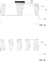
Fig. 2A shows a schematic cross-sectional view illustrating one stage of a manufacturing method of a semiconductor apparatus in accordance with one or more embodiments of the present invention, viewed from a first direction. -
Fig. 2B shows another schematic cross-sectional view of the component shown inFig. 2A , viewed from a second direction. -
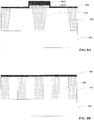
Fig. 3A shows a schematic cross-sectional view illustrating one stage of a manufacturing method of a semiconductor apparatus in accordance with one or more embodiments of the present invention, viewed from the first direction. -
Fig. 3B shows another schematic cross-sectional view of the component shown inFig. 3A , viewed from the second direction. -
Figs. 4 and 5A each show a schematic cross-sectional view illustrating one stage of a manufacturing method of a semiconductor apparatus in accordance with one or more embodiments of the present invention, viewed from the first direction. -
Fig. 5B shows another schematic cross-sectional view of the component shown inFig. 5A , viewed from the second direction. -
Figs. 6 and7A each show a schematic cross-sectional view illustrating one stage of a manufacturing method of a semiconductor apparatus in accordance with one or more embodiments of the present invention, viewed from the first direction. -
Fig. 7B shows another schematic cross-sectional view of the component shown inFig. 7A , viewed from the second direction. -
Fig. 8A shows a schematic cross-sectional view illustrating one stage of a manufacturing method of a semiconductor apparatus in accordance with one or more embodiments of the present invention, viewed from the first direction. -
Fig. 8B shows another schematic cross-sectional view of the component shown inFig. 8A , viewed from the second direction. -
Fig. 9A shows a schematic cross-sectional view illustrating one stage of a manufacturing method of a semiconductor apparatus in accordance with one or more embodiments of the present invention, viewed from the first direction. -
Fig. 9B shows another schematic cross-sectional view of the component shown inFig. 9A , viewed from the second direction. -
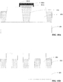
Fig. 10A shows a schematic cross-sectional view illustrating one stage of a manufacturing method of a semiconductor apparatus in accordance with one or more embodiments of the present invention, viewed from the first direction. -
Fig. 10B shows another schematic cross-sectional view of the component shown inFig. 10A , viewed from the second direction. -
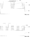
Fig. 11A shows a schematic cross-sectional view illustrating one stage of a manufacturing method of a semiconductor apparatus in accordance with one or more embodiments of the present invention, viewed from the first direction. -
Fig. 11B shows another schematic cross-sectional view of the component shown inFig. 11A , viewed from the second direction. -
Figs. 12, 13 ,14, and 15A each show a schematic cross-sectional view illustrating one stage of a manufacturing method of a semiconductor apparatus in accordance with one or more embodiments of the present invention, viewed from the first direction. -
Fig. 15B shows another schematic cross-sectional view of the component shown inFig. 15A , viewed from the second direction. -
Fig. 16A shows a schematic cross-sectional view illustrating one stage of a manufacturing method of a semiconductor apparatus in accordance with one or more embodiments of the present invention, viewed from the first direction. -
Fig. 16B shows another schematic cross-sectional view of the component shown inFig. 16A , viewed from the second direction. -
Fig. 17A shows a schematic cross-sectional view illustrating one stage of a manufacturing method of a semiconductor apparatus in accordance with one or more embodiments of the present invention, viewed from the first direction. -
Fig. 17B shows another schematic cross-sectional view of the component shown inFig. 17A , viewed from the second direction. -
Fig. 18A shows a schematic cross-sectional view illustrating one stage of a manufacturing method of a semiconductor apparatus in accordance with one or more embodiments of the present invention, viewed from the first direction. -
Fig. 18B shows another schematic cross-sectional view of the component shown inFig. 18A , viewed from the second direction. -
Fig. 19A shows a schematic cross-sectional view illustrating one stage of a manufacturing method of a semiconductor apparatus in accordance with one or more embodiments of the present invention, viewed from the first direction. -
Fig. 19B shows another schematic cross-sectional view of the component shown inFig. 19A , viewed from the second direction. - Example embodiments of the present invention are described with reference to the accompanying drawings. As those skilled in the art would realize, the described embodiments may be modified in various ways without departing from the present invention defined in the claims. Embodiments may be practiced without some or all of these specified details. Well known process steps and/or structures may not be described in detail, in the interest of clarity.
- The drawings and descriptions are illustrative and not restrictive. Like reference numerals may designate like (e.g., analogous or identical) elements in the specification. To the extent possible, any repetitive description will be minimized.
- Relative sizes and thicknesses of elements shown in the drawings are chosen to facilitate description and understanding, without limiting the present invention. In the drawings, the thicknesses of some layers, films, panels, regions, etc., may be exaggerated for clarity.
- Embodiments in the figures may represent idealized illustrations. Variations from the shapes illustrated may be possible, for example due to manufacturing techniques and/or tolerances. Thus, the example embodiments shall not be construed as limited to the shapes or regions illustrated herein but are to include deviations in the shapes. For example, an etched region illustrated as a rectangle may have rounded or curved features. The shapes and regions illustrated in the figures are illustrative and shall not limit the invention.
- Although the terms "first," "second," etc. may be used herein to describe various elements, these elements shall not be limited by these terms. These terms may be used to distinguish one element from another element. Thus, a first element discussed below may be termed a second element without departing from the teachings of the present invention. The description of an element as a "first" element may not require or imply the presence of a second element or other elements. The terms "first," "second," etc. may also be used herein to differentiate different categories or sets of elements. For conciseness, the terms "first," "second," etc. may represent "first-category (or first-set)," "second-category (or second-set)," etc., respectively.
- If a first element (such as a layer, film, region, or substrate) is referred to as being "on," "neighboring," "connected to," or "coupled with" a second element, then the first element can be directly on, directly neighboring, directly connected to or directly coupled with the second element, or an intervening element may also be present between the first element and the second element. If a first element is referred to as being "directly on," "directly neighboring," "directly connected to," or "directly coupled with" a second element, then no intended intervening element (except environmental elements such as air) may also be present between the first element and the second element.
- Spatially relative terms, such as "beneath," "below," "lower," "above," "upper," and the like, may be used herein for ease of description to describe one element or feature's spatial relationship to another element(s) or feature(s) as illustrated in the figures. It will be understood that the spatially relative terms may encompass different orientations of the device in use or operation in addition to the orientation depicted in the figures. For example, if the device in the figures is turned over, elements described as "below" or "beneath" other elements or features would then be oriented "above" the other elements or features. Thus, the term "below" can encompass both an orientation of above and below. The device may be otherwise oriented (rotated 90 degrees or at other orientation), and the spatially relative descriptors used herein shall be interpreted accordingly.
- The terminology used herein is for the purpose of describing particular embodiments and is not intended to limit the present invention. As used herein, singular forms, "a," "an," and "the" may indicate plural forms as well, unless the context clearly indicates otherwise. The terms "includes" and/or "including," when used in this specification, may specify the presence of stated features, integers, steps, operations, elements, and/or components, but may not preclude the presence or addition of one or more other features, integers, steps, operations, elements, components, and/or groups.
- Unless otherwise defined, terms (including technical and scientific terms) used herein have the same meanings as what is commonly understood by one of ordinary skill in the art related to this field. Terms, such as those defined in commonly used dictionaries, shall be interpreted as having meanings that are consistent with their meanings in the context of the relevant art and shall not be interpreted in an idealized or overly formal sense unless expressly so defined herein.
- The term "connect" may mean "electrically connect." The term "insulate" may mean "electrically insulate."
- Unless explicitly described to the contrary, the word "comprise" and variations such as "comprises," "comprising," "include," or "including" may imply the inclusion of stated elements but not the exclusion of other elements.
- Various embodiments, including methods and techniques, are described in this disclosure. Embodiments of the present invention may also cover an article of manufacture that includes a non-transitory computer readable medium on which computer-readable instructions for carrying out embodiments of the inventive technique are stored. The computer readable medium may include, for example, semiconductor, magnetic, opto-magnetic, optical, or other forms of computer readable medium for storing computer readable code. Further, the present invention may also cover apparatuses for practicing embodiments of the present invention. Such apparatus may include circuits, dedicated and/or programmable, to carry out operations pertaining to embodiments of the present invention. Examples of such apparatus include a general purpose computer and/or a dedicated computing device when appropriately programmed and may include a combination of a computer/computing device and dedicated/programmable hardware circuits (such as electrical, mechanical, and/or optical circuits) adapted for the various operations pertaining to embodiments of the present invention.
-
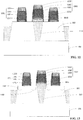
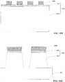
Fig. 1 shows a flowchart illustrating simplified procedures in a manufacturing method of a semiconductor apparatus in accordance with one or more embodiments of this present invention.Figs. 2A, 2B ,3A, 3B ,4, 5A ,5B, 6 ,7A, 7B ,8A, 8B ,9A, 9B ,10A, 10B ,11A, and 11B show schematic cross-sectional views illustrating different stages of a manufacturing method of a semiconductor apparatus in accordance with one or more embodiments of this present invention. Referring to these Figures, a manufacturing method of a semiconductor apparatus in accordance with one or more embodiments of this present invention is described below. - Referring to
Fig. 1 , instep 102, provide a substrate structure.Fig. 2A shows a schematic cross-sectional view illustrating one stage of a manufacturing method of a semiconductor apparatus in accordance with one or more embodiments of this present invention, viewed from a first direction.Fig. 2B shows another schematic cross-sectional view of the component shown inFig. 2A , viewed from a second direction. The cross-sectional view inFig. 2B is obtained by observing the component inFig. 2A at a plane that includes line B-B' and is perpendicular to the paper, the second direction is the direction of the arrows in line B-B', as shown inFig. 2A . - Referring to
Figs. 2A and 2B , the substrate structure comprises asubstrate 201, which may be a silicon (Si) substrate, a silicon-on-insulator (SOI) substrate, or a III-V group substrate. - The substrate structure further comprises one or
multiple fins 202 on thesubstrate 201 positioned along the first direction. The first direction is a direction along which thefins 202 extends and is also called the channel direction. Thefins 202 may be made of the same material of thesubstrate 201, but can also be made of a different material. - The substrate structure further comprises a separation region surrounding the
fins 202. An upper surface of the separation region is on a substantially same horizontal level with an upper surface of thefins 202. The separation region comprises afirst separation region 213 neighboring a first side of thefins 202 along the first direction, and asecond separation region 223 neighboring a second side of thefins 202 along the second direction. The second direction may be any direction that is perpendicular to the first direction, and is also called the perpendicular-to-channel direction. Thefirst separation region 213 may locate on one or both sides of thefins 202 along the first direction, thesecond separation region 223 may locate on one or both sides of thefins 202 along the second direction. In one embodiment, the separation region may be made of dielectric materials such as oxide, nitride, or nitrogen oxide. - Referring to
Figs. 3A and 3B , instep 104, form afirst insulation layer 301 on the substrate structure, form asecond insulation layer 302 on thefirst insulation layer 301. Optimally, thefirst insulation layer 301 and thesecond insulation layer 302 may have different etching ratios. In one embodiment, thefirst insulation layer 301 may be an oxide layer, such as a silicon oxide layer, thesecond insulation layer 302 may be a nitride layer, such as a silicon nitride layer. Thefirst insulation layer 301 and thesecond insulation layer 302 may also be made of other materials. - Referring to
Fig. 4 , instep 106, form abarrier layer 401 to cover a first portion of thesecond insulation layer 302 on thefirst separation region 213. In one embodiment, thebarrier layer 401 may further cover a portion of thesecond insulation layer 302 on the upper surface of thefins 202 neighboring thefirst separation region 213. In other words, the width of thebarrier layer 401 in the first direction is greater than or equal to the largest width of thefirst separation region 213 in the first direction. In one embodiment, thebarrier layer 401 may be formed by first forming a photoresist layer on thesecond insulation layer 302 and then performing a patternization process on the photoresist. The patternization process may be a Single Diffusion Break (SDB) process. -
Fig. 4 only shows thebarrier layer 401 formed on thefirst separation region 213 located between twofins 202. In other embodiments, thebarrier layer 401 may also be formed on the separation regions neighboring the other side of thefins 202 along the first direction. - Referring to
Figs. 5A and5B , instep 108, perform a first etching process using thebarrier layer 401 as a mask to remove a second portion of thesecond insulation layer 302 that is not covered by thebarrier layer 401. The first portion of thesecond insulation layer 302 is retained and is annotated as a remainingsecond insulation layer 302A. In one embodiment, the first etching process may be a wet etching or a dry etching process. In one embodiment, the first etching process will stop upon reaching thefirst insulation layer 301. - Referring to
Fig. 6 , instep 110, remove thebarrier layer 401 to expose the remainingsecond insulation layer 302A. - Referring to
Figs. 7A and 7B , instep 112, perform a second etching process using the remainingsecond insulation layer 302A as a mask to remove a portion of thefirst insulation layer 301 that is not covered by the remainingsecond insulation layer 302A. The portion of thefirst insulation layer 301 underneath the remainingsecond insulation layer 302A is retained and is annotated as a remainingfirst insulation layer 301A. In one embodiment, the second etching process will stop upon reaching the upper surface of thefins 202 or the upper surface of the separation regions surrounding thefins 202. - Referring to
Figs. 8A and 8B , instep 114, form athird insulation layer 801A on side surfaces of the remainingfirst insulation layer 301 A and the remainingsecond insulation layer 302A. In one embodiment, aninsulation material layer 801 is first deposited on the upper surface of thefins 202 and the upper surface of the separation regions that are not covered by the remainingfirst insulation layer 301 A or the remainingsecond insulation layer 302A, on the side surfaces of the remainingfirst insulation layer 301A and the remainingsecond insulation layer 302A, and on an upper surface of the remainingsecond insulation layer 302A. Referring toFigs. 9A and 9B , use an anisotropy etching process to remove a portion of theinsulation material layer 801 that is on the upper surfaces of thefins 202 and the upper surface of the separation regions that are not covered by the remainingfirst insulation layer 301A and the remainingsecond insulation layer 302A, and on the upper surface of the remainingsecond insulation layer 302A. A portion of theinsulation material layer 801 on the side surfaces of the remainingfirst insulation layer 301 A and the remainingsecond insulation layer 302A is retained and is annotated as thethird insulation layer 801A. Optimally, thethird insulation layer 801 A and thesecond insulation layer 302 may be made of the same material. In one embodiment, both thethird insulation layer 801 A and thesecond insulation layer 302 are a nitride layer, such as a silicon nitride layer. - In some embodiments, the
third insulation layer 801 A may also be formed on the upper surface of the remainingsecond insulation layer 302A. In that case, after theinsulation material layer 801 is deposited, only a portion of theinsulation material layer 801 on the upper surface of the remainingsecond insulation layer 302A will be removed, the rest of them will be retained on the upper surface of the remainingsecond insulation layer 302A and become part of thethird insulation layer 801 A. - Referring to
Figs. 10A and 10B , instep 116, perform a third etching process using the remainingsecond insulation layer 302A and thethird insulation layer 801 A as a mask to remove a portion of thesecond separation region 223, so that an upper surface of the remainingsecond separation region 223 is lower than the upper surface of thefins 202. During the third etching process, the remainingfirst insulation layer 301A is protected by the remainingsecond insulation layer 302A and thethird insulation layer 801A and is not removed. The third etching process removes a portion of the separation region that is not covered by the remainingfirst insulation layer 301A, including the second separation region and a portion of the separation region neighboring the first side of thefins 202 along the first direction. After the third etching process, the upper surface of the separation region that is not covered by the remainingfirst insulation layer 301 A is lower than the upper surface of thefins 202. - Referring to
Figs. 11A and 11B , instep 118, remove the remainingsecond insulation layer 302A and thethird insulation layer 801A. The remainingfirst insulation layer 301A on thefirst separation region 213 is retained. - This concludes the description of a manufacturing method of a semiconductor apparatus in accordance with one embodiment of this present invention. The
first separation region 213 and thesecond separation region 223 have different heights, and the upper surface of thefirst separation region 213 is on a substantially same horizontal level as the upper surface of thefins 202, and is covered by the remainingfirst insulation layer 301 A. Therefore, when dummy gate structures are formed on thefirst insulation layer 301 in succeeding stages, the dummy gate structures will not bridge the fins even with some deviations of their positions. This effectively reduces the electrical leakage and improves the reliability of the devices. Additionally, the dummy gate structures, even with some deviations on their positions, will not affect the contour of the epitaxially grown semiconductor materials and therefore will not affect the induced stress in the channel, which improves the migration rate of charge carriers in the semiconductor device. In this method, thethird insulation layer 801 A is formed on the side surfaces of the remainingfirst insulation layer 301A and the remainingsecond insulation layer 302A before a portion of thesecond separation region 223 is removed, thethird insulation layer 801A can protect the remainingfirst insulation layer 301A from being damaged. - Referring to
Figs. 11A and 11B , a semiconductor apparatus made with a manufacturing method in accordance with one or more embodiments of the present invention is described below. - The semiconductor apparatus comprises a
substrate 201; one ormultiple fins 202 positioned along a first direction on thesubstrate 201; and a separation region surrounding thefins 202. The separation region comprises afirst separation region 213 neighboring a first side of thefins 202 along the first direction, and asecond separation region 223 neighboring a second side of thefins 202 along a second direction that is different from the first direction. An upper surface of thefirst separation region 213 is on a substantially same horizontal level with an upper surface of thefins 202, an upper surface of thesecond separation region 223 is lower than the upper surface of thefins 202. The semiconductor apparatus further comprises afirst insulation layer 301A on thefirst separation region 213. In one embodiment, thefirst insulation layer 301A may further cover a portion of the upper surface of thefins 202 neighboring thefirst separation region 213. - Referring to
Fig. 12 , in one embodiment, after the semiconductor apparatus shown inFigs. 11A and 11B is formed, the manufacturing method further comprises: forming afirst gate structure 1201 on thefins 202, forming asecond gate structure 1202 on the remainingfirst insulation layer 301 A. Usually, thesecond gate structure 1202 is a dummy gate structure. - In one embodiment, the
first gate structure 1201 comprises afirst dielectric layer 1211, which may be made of silicon oxide, on thefins 202; afirst gate 1221, which may be made of poly-crystalline silicon, on thefirst dielectric layer 1211; a firsthard mask layer 1231, which may be made of silicon nitride, on thefirst gate 1221; andfirst separation objects 1241, which may be made of silicon oxide or silicon nitride, formed on side surfaces of thefirst dielectric layer 1211, thefirst gate 1221, and the firsthard mask layer 1231. - In one embodiment, the
second gate structure 1202 comprises asecond dielectric layer 1212, which may be made of silicon oxide, on the remainingfirst insulation layer 301 A; asecond gate 1222, which may be made of poly-crystalline silicon, on thesecond dielectric layer 1212; a secondhard mask layer 1232, which may be made of silicon nitride, on thesecond gate 1222; andsecond separation object 1242, which may be made of silicon oxide or silicon nitride, formed on side surfaces of thesecond dielectric layer 1212, thesecond gate 1222, and the secondhard mask layer 1232. Thesecond separation objects 1242 covers a portion of the upper surface of thefins 202 neighboring thefirst separation region 213 that is underneath thesecond gate structure 1202. - In one embodiment, after the
first gate structure 1201 and thesecond gate structure 1202 are formed, the manufacturing method further comprises the following steps. - Referring to
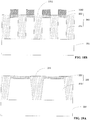
Fig. 13 , etch thefins 202 on two sides of thefirst gate structure 1201 using thefirst gate structure 1201 and thesecond gate structure 1202 as masks to form dents such as thefirst dent 1321 and thesecond dent 1322. Referring toFig. 14 , epitaxially grow semiconductor materials in thefirst dent 1321 and thesecond dent 1322 to form asource region 1401 and adrain region 1402, respectively. In one embodiment, the semiconductor materials in thefirst dent 1321 and thesecond dent 1322 may be silicon-germanium (SiGe), silicon carbide (SiC), or silicon. When silicon is used as the semiconductor material in thefirst dent 1321 and thesecond dent 1322, Phosphorus can be in-situ doped. - Referring to
Fig. 14 , the present invention also presents another semiconductor apparatus. Comparing with the semiconductor apparatus shown inFigs. 11A and 11B , the semiconductor apparatus shown inFig. 14 further comprises afirst gate structure 1201 on thefins 202, and asecond gate structure 1202 on the remainingfirst insulation layer 301A. Additionally, this semiconductor apparatus further comprises asource region 1401 and adrain region 1402, which are formed by epitaxially growing semiconductor materials on two sides of thefirst gate structure 1201. In one embodiment, thefirst gate structure 1201 and thesecond gate structure 1202 may have the same structures as those disclosed in the manufacturing method described above, which are not repeated here in the interest of conciseness. - In this semiconductor apparatus, an upper surface of the first separation region is on a substantially same horizontal level with the upper surface of the fins, and the first insulation layer is formed on the first separation region. Therefore, when dummy gate structures, such as the second gate structure as shown in
Fig. 14 , are formed on the first insulation layer, these gate structures will not connect with the fins even if there are some deviations on their positions. This effectively reduces the electrical leakage and improves the reliability of the devices. Additionally, the dummy gate structures, even with some deviations on their positions, will not affect the contour of the epitaxially grown semiconductor materials and therefore will not affect the induced stress in the channel, which improves the migration rate of charge carriers in the semiconductor device. - Referring to
Figs. 15A ,15B ,16A ,16B ,17A ,17B ,18A ,18B ,19A , and19B , the present invention further presents an embodiment of a manufacturing method for the substrate structure described above. - Referring to
Figs. 15A and15B , provide aninitial substrate 1501, form ahard mask layer 1502 on theinitial substrate 1501. Thehard mask layer 1502 may be formed by self-aligned double patterning (SADP) technique and may be made of silicon nitride. In one embodiment, theinitial substrate 1501 comprises aninitial semiconductor layer 1511 and aninitial oxide layer 1521 on theinitial semiconductor layer 1501. Theinitial oxide layer 1521 may work as a buffer layer to reduce the stress between theinitial substrate 1501 and thehard mask layer 1502. - Referring to
Figs. 16A and16B , etch theinitial substrate 1501 using thehard mask layer 1502 as a mask to form thesubstrate 201 and one ormultiple fins 202 on thesubstrate 201. In one embodiment, theinitial substrate 1501 comprises theinitial semiconductor layer 1511 and theinitial oxide layer 1521 on theinitial semiconductor layer 1501. Therefore thefins 202 also comprises asemiconductor layer 212 and anoxide layer 222 on thesemiconductor layer 212. - Referring to
Figs. 17A and17B ,separation material 1701 is deposited around thefins 202 to fill the area surrounding thefins 202. An upper surface of theseparation material 1701 is on a substantially same horizontal level with an upper surface of thehard mask layer 1502. As an example, theseparation material 1701 may be deposited by Flowable Chemical Vapor Deposition (FCVD) followed by a planarization process such as Chemical-Mechanical Polishing (CMP), so that the upper surface of theseparation material 1701 is on a substantially same horizontal level with the upper surface of thehard mask layer 1502. Additionally, in another embodiment, before theseparation material 1701 is deposited, a liner layer may be formed on the structure shown inFig. 16A , the liner layer may be a silicon oxide layer and may be formed by an In-Situ Steam Generation (ISSG) process. The liner layer may fix defects that may exist on fins' surfaces. - Referring to
Figs. 18A and18B , etch back theseparation layer 1701 to expose thehard mask layer 1502. - Referring to
Figs. 19A and19B , remove thehard mask layer 1502 to form the substrate structure. - Compared with the substrate structure shown in
Figs. 2A and 2B , the substrate structure shown inFigs. 19A and19B has anadditional oxide layer 222. Theoxide layer 222 is optional. - After the substrate structure is formed, the steps shown in
Fig. 1 may be performed on the substrate structure according to the description above.
Claims (15)
- A method for manufacturing a semiconductor apparatus, comprising:providing a substrate structure, wherein the substrate structure comprises:a substrate;one or multiple fins positioned along a first direction on the substrate; anda separation region surrounding the fins,wherein an upper surface of the separation region is on a substantially same horizontal level as an upper surface of the fins, the separation region comprises a first separation region neighboring a first side of the fins along the first direction, and a second separation region neighboring a second side of the fins along a second direction that is different from the first direction;forming a first insulation layer on the substrate structure;forming a second insulation layer on the first insulation layer;forming a barrier layer on a first portion of the second insulation layer on the first separating region;performing a first etching process using the barrier layer as a mask to remove a second portion of the second insulation layer that is not covered by the barrier layer;removing the barrier layer;performing a second etching process using the remaining second insulation layer as a mask to remove a portion of the first insulation layer that is not covered by the remaining second insulation layer;forming a third insulation layer on side surfaces of the remaining first insulation layer and the remaining second insulation layer;performing a third etching process using the remaining second insulation layer and the third insulation layer as a mask to remove a portion of the second separation region that is not covered by the remaining second insulation layer or the third insulation layer; andremoving the remaining second insulation layer and the third insulation layer.
- The method of claim 1, wherein the barrier layer further covers a portion of the second insulation layer on the upper surface of the fins neighboring the first separation region.
- The method of claim 1 or 2, wherein forming a third insulation layer on side surfaces of the remaining first insulation layer and the remaining second insulation layer comprises:forming an insulation material layer to cover a surface that is not covered by either the remaining first insulation layer or the remaining second insulation layer, side surfaces of the remaining first insulation layer and the remaining second insulation layer, and an upper surface of the remaining second insulation layer; andremoving a portion of the insulation material layer on the surface that is not covered by the remaining first insulation layer and the remaining second insulation layer, and on the upper surface of the remaining second insulation layer, the remaining insulation material layer is the third insulation layer.
- The method of anyone of the claims 1-3, wherein
the first insulation layer and the second insulation layer have different etching ratios; and/or
the first insulation layer is an oxide layer, the second insulation layer is a nitride layer, and the third insulation layer is a nitride layer. - The method of anyone of the claims 1-4, wherein providing a substrate structure comprises:providing an initial substrate;forming a patterned hard mask layer on the initial substrate;etching the initial substrate using the hard mask layer as a mask to form the substrate and one or multiple fins on the substrate;depositing separation material to fill areas surrounding the fins, wherein an upper surface of the separation material is on a substantially same horizontal level with an upper surface of the hard mask layer;etching back the separation material to expose the hard mask layer; andremoving the hard mask layer to form the substrate structure; andwherein preferably: the initial substrate comprises an initial semiconductor layer and an initial oxide layer on the initial semiconductor layer, the fins comprises a semiconductor layer and an oxide layer on the semiconductor layer.
- The method of anyone of the claims 1-5, further comprising:forming a first gate structure on the fins; andforming a second gate structure on the remaining first insulation layer.
- The method of claim 6, further comprising:etching the fins on two sides of the first gate structure using the first gate structure and the second gate structure as masks to form dents; andepitaxially growing semiconductor materials in the dents to form a source region and a drain region; andwherein preferably: the semiconductor materials comprise silicon-germanium (SiGe) or silicon carbide (SiC).
- The method of claim 6 or 7, wherein the first gate structure comprises:a first dielectric layer on the fins;a first gate on the first dielectric layer;a first hard mask layer on the first gate; andfirst separation objects on side surfaces of the first dielectric layer, the first gate, and the first hard mask layer,wherein the second gate structure comprises:a second dielectric layer on the remaining first insulation layer;a second gate on the second dielectric layer;a second hard mask layer on the second gate; andsecond separation objects on side surfaces of the second dielectric layer, the second gate, and the second hard mask layer, wherein the second separation objects cover a portion of the upper surface of the fins next to the first separation region that is underneath the second gate structure; andwherein preferably: the first dielectric layer and the second dielectric layer are made of silicon oxide, the first gate and the second gate are made of poly-crystalline silicon, and the first hard mask layer and the second hard mask layer are made of silicon nitride.
- A semiconductor apparatus, comprising:a substrate;one or multiple fins positioned along a first direction on the substrate;a separation region surrounding the fins, wherein the separation region comprises a first separation region neighboring a first side of the fins along the first direction, and a second separation region neighboring a second side of the fins along a second direction that is different from the first direction, wherein an upper surface of the first separation region is on a substantially same horizontal level with an upper surface of the fins, and wherein an upper surface of the second separation region is lower than the upper surface of the fins; anda first insulation layer on the first separation region.
- The apparatus of claim 9, wherein the first insulation layer further covers a portion of the upper surfaces of the fins next to the first separation region.
- The apparatus of claim 9 or 10, further comprising:a first gate structure on the fins; anda second gate structure on the first insulation layer.
- The apparatus of claim 11, further comprising:a source region next to a first side of the first gate structure formed by epitaxially growing a semiconductor material; anda drain region next to a second side of the first gate structure formed by epitaxially growing the semiconductor material.
- The apparatus of claim 12, wherein the semiconductor material comprises silicon-germanium (SiGe) or silicon carbide (SiC).
- The apparatus of claim 12 or 13, wherein the first dielectric layer and the second dielectric layer are made of silicon oxide, the first gate and the second gate are made of poly-crystalline silicon, and the first hard mask layer and the second hard mask layer are made of silicon nitride.
- The apparatus of anyone of the claims 11-14, wherein the first gate structure comprises:a first dielectric layer on the fins;a first gate on the first dielectric layer;a first hard mask layer on the first gate; andfirst separation objects on side surfaces of the first dielectric layer, the first gate, and the first hard mask layer,wherein the second gate structure comprises:a second dielectric layer on the remaining first insulation layer;a second gate on the second dielectric layer;a second hard mask layer on the second gate; andsecond separation objects on side surfaces of the second dielectric layer, the second gate, and the second hard mask layer, wherein the second separation objects cover a portion of the upper surface of the fins next to the first separation region that is underneath the second gate structure.
Applications Claiming Priority (1)
| Application Number | Priority Date | Filing Date | Title |
|---|---|---|---|
| CN201610900638.XA CN107958933B (en) | 2016-10-17 | 2016-10-17 | Semiconductor device and method of manufacturing the same |
Publications (1)
| Publication Number | Publication Date |
|---|---|
| EP3309842A1 true EP3309842A1 (en) | 2018-04-18 |
Family
ID=60119883
Family Applications (1)
| Application Number | Title | Priority Date | Filing Date |
|---|---|---|---|
| EP17196526.2A Withdrawn EP3309842A1 (en) | 2016-10-17 | 2017-10-16 | A semiconductor apparatus and manufacturing method |
Country Status (3)
| Country | Link |
|---|---|
| US (2) | US10256153B2 (en) |
| EP (1) | EP3309842A1 (en) |
| CN (1) | CN107958933B (en) |
Families Citing this family (2)
| Publication number | Priority date | Publication date | Assignee | Title |
|---|---|---|---|---|
| US10770589B2 (en) * | 2018-08-21 | 2020-09-08 | International Business Machines Corporation | Fin field effect transistor including a single diffusion break with a multi-layer dummy gate |
| US11127834B2 (en) * | 2019-10-11 | 2021-09-21 | Globalfoundries U.S. Inc | Gate structures |
Citations (5)
| Publication number | Priority date | Publication date | Assignee | Title |
|---|---|---|---|---|
| US20150147860A1 (en) * | 2013-11-27 | 2015-05-28 | Samsung Electronics Co., Ltd. | Methods of fabricating semiconductor devices |
| US20160079125A1 (en) * | 2014-09-11 | 2016-03-17 | Samsung Electronics Co., Ltd. | Semiconductor devices and methods of manufacturing the same |
| US9368496B1 (en) * | 2015-01-30 | 2016-06-14 | Globalfoundries Inc. | Method for uniform recess depth and fill in single diffusion break for fin-type process and resulting devices |
| US20160225848A1 (en) * | 2015-01-30 | 2016-08-04 | Globalfoundries Inc. | Process for single diffusion break with simplfied process |
| EP3163628A1 (en) * | 2015-10-28 | 2017-05-03 | Semiconductor Manufacturing International Corporation (Beijing) | Semiconductor device and fabrication method for forming the same |
Family Cites Families (8)
| Publication number | Priority date | Publication date | Assignee | Title |
|---|---|---|---|---|
| US9337318B2 (en) * | 2012-10-26 | 2016-05-10 | Taiwan Semiconductor Manufacturing Company, Ltd. | FinFET with dummy gate on non-recessed shallow trench isolation (STI) |
| US9330959B2 (en) * | 2014-04-13 | 2016-05-03 | Texas Instruments Incorporated | Isolated semiconductor layer in bulk wafer by localized silicon epitaxial seed formation |
| WO2016039213A1 (en) * | 2014-09-12 | 2016-03-17 | 住友ベークライト株式会社 | Lignin derivative, lignin resin composition, rubber composition, and molding material |
| CN106340455B (en) * | 2015-07-06 | 2021-08-03 | 联华电子股份有限公司 | Semiconductor device and method of making the same |
| US9716042B1 (en) * | 2015-12-30 | 2017-07-25 | International Business Machines Corporation | Fin field-effect transistor (FinFET) with reduced parasitic capacitance |
| US9941386B2 (en) * | 2016-06-01 | 2018-04-10 | Taiwan Semiconductor Manufacturing Co., Ltd. | Semiconductor device structure with fin structure and method for forming the same |
| US20170373144A1 (en) * | 2016-06-28 | 2017-12-28 | GlobalFoundries, Inc. | Novel sti process for sdb devices |
| CN107958871B (en) * | 2016-10-17 | 2020-10-30 | 中芯国际集成电路制造(上海)有限公司 | Semiconductor device and method for manufacturing the same |
-
2016
- 2016-10-17 CN CN201610900638.XA patent/CN107958933B/en active Active
-
2017
- 2017-10-16 EP EP17196526.2A patent/EP3309842A1/en not_active Withdrawn
- 2017-10-17 US US15/786,250 patent/US10256153B2/en active Active
-
2019
- 2019-03-04 US US16/291,846 patent/US10804157B2/en active Active
Patent Citations (5)
| Publication number | Priority date | Publication date | Assignee | Title |
|---|---|---|---|---|
| US20150147860A1 (en) * | 2013-11-27 | 2015-05-28 | Samsung Electronics Co., Ltd. | Methods of fabricating semiconductor devices |
| US20160079125A1 (en) * | 2014-09-11 | 2016-03-17 | Samsung Electronics Co., Ltd. | Semiconductor devices and methods of manufacturing the same |
| US9368496B1 (en) * | 2015-01-30 | 2016-06-14 | Globalfoundries Inc. | Method for uniform recess depth and fill in single diffusion break for fin-type process and resulting devices |
| US20160225848A1 (en) * | 2015-01-30 | 2016-08-04 | Globalfoundries Inc. | Process for single diffusion break with simplfied process |
| EP3163628A1 (en) * | 2015-10-28 | 2017-05-03 | Semiconductor Manufacturing International Corporation (Beijing) | Semiconductor device and fabrication method for forming the same |
Also Published As
| Publication number | Publication date |
|---|---|
| US10256153B2 (en) | 2019-04-09 |
| CN107958933B (en) | 2020-05-26 |
| US20180108569A1 (en) | 2018-04-19 |
| CN107958933A (en) | 2018-04-24 |
| US10804157B2 (en) | 2020-10-13 |
| US20190206737A1 (en) | 2019-07-04 |
Similar Documents
| Publication | Publication Date | Title |
|---|---|---|
| US10872805B2 (en) | Semiconductor device and manufacturing method thereof | |
| TWI575608B (en) | A venting overburden structure for a base fin field effect transistor that does not depend on the gate length | |
| US10236216B2 (en) | Method for manufacturing a semiconductor device having a fin located on a substrate | |
| US9105746B2 (en) | Method for manufacturing a field effect transistor of a non-planar type | |
| US10615278B2 (en) | Preventing strained fin relaxation | |
| US10211320B2 (en) | Fin cut without residual fin defects | |
| US9666709B2 (en) | Non-planar semiconductor structure with preserved isolation region | |
| US10622441B2 (en) | Semiconductor apparatus and manufacturing method for same | |
| US10818556B2 (en) | Method for forming a semiconductor structure | |
| US9722024B1 (en) | Formation of semiconductor structures employing selective removal of fins | |
| US20200258787A1 (en) | Semiconductor device | |
| US10804157B2 (en) | Semiconductor apparatus and manufacturing method | |
| CN112309977B (en) | Semiconductor structures and methods of forming them | |
| US10043675B2 (en) | Semiconductor device and method for fabricating the same | |
| US9847423B1 (en) | Semiconductor device and method for fabricating the same | |
| US20070132031A1 (en) | Semiconductor device having stressors and method for forming | |
| US9508588B2 (en) | Methods for fabricating integrated circuits with isolation regions having uniform step heights | |
| EP3723112A1 (en) | Method for forming a gate mask layer | |
| CN106910685A (en) | A kind of semiconductor devices and preparation method thereof, electronic installation | |
| CN110707041A (en) | Semiconductor structure and forming method thereof | |
| EP2693462A1 (en) | Method for manufacturing semiconductor devices |
Legal Events
| Date | Code | Title | Description |
|---|---|---|---|
| PUAI | Public reference made under article 153(3) epc to a published international application that has entered the european phase |
Free format text: ORIGINAL CODE: 0009012 |
|
| STAA | Information on the status of an ep patent application or granted ep patent |
Free format text: STATUS: THE APPLICATION HAS BEEN PUBLISHED |
|
| AK | Designated contracting states |
Kind code of ref document: A1 Designated state(s): AL AT BE BG CH CY CZ DE DK EE ES FI FR GB GR HR HU IE IS IT LI LT LU LV MC MK MT NL NO PL PT RO RS SE SI SK SM TR |
|
| AX | Request for extension of the european patent |
Extension state: BA ME |
|
| STAA | Information on the status of an ep patent application or granted ep patent |
Free format text: STATUS: REQUEST FOR EXAMINATION WAS MADE |
|
| 17P | Request for examination filed |
Effective date: 20180619 |
|
| RBV | Designated contracting states (corrected) |
Designated state(s): AL AT BE BG CH CY CZ DE DK EE ES FI FR GB GR HR HU IE IS IT LI LT LU LV MC MK MT NL NO PL PT RO RS SE SI SK SM TR |
|
| RAP1 | Party data changed (applicant data changed or rights of an application transferred) |
Owner name: SEMICONDUCTOR MANUFACTURING INTERNATIONAL (BEIJING Owner name: SEMICONDUCTOR MANUFACTURING INTERNATIONAL (SHANGHA |
|
| STAA | Information on the status of an ep patent application or granted ep patent |
Free format text: STATUS: EXAMINATION IS IN PROGRESS |
|
| 17Q | First examination report despatched |
Effective date: 20200619 |
|
| STAA | Information on the status of an ep patent application or granted ep patent |
Free format text: STATUS: THE APPLICATION IS DEEMED TO BE WITHDRAWN |
|
| 18D | Application deemed to be withdrawn |
Effective date: 20201030 |