EP3309605A1 - Display device - Google Patents
Display device Download PDFInfo
- Publication number
- EP3309605A1 EP3309605A1 EP17195978.6A EP17195978A EP3309605A1 EP 3309605 A1 EP3309605 A1 EP 3309605A1 EP 17195978 A EP17195978 A EP 17195978A EP 3309605 A1 EP3309605 A1 EP 3309605A1
- Authority
- EP
- European Patent Office
- Prior art keywords
- subpixel
- pixel
- disposed
- light blocking
- blocking member
- Prior art date
- Legal status (The legal status is an assumption and is not a legal conclusion. Google has not performed a legal analysis and makes no representation as to the accuracy of the status listed.)
- Granted
Links
Images






Classifications
-
- G—PHYSICS
- G02—OPTICS
- G02F—OPTICAL DEVICES OR ARRANGEMENTS FOR THE CONTROL OF LIGHT BY MODIFICATION OF THE OPTICAL PROPERTIES OF THE MEDIA OF THE ELEMENTS INVOLVED THEREIN; NON-LINEAR OPTICS; FREQUENCY-CHANGING OF LIGHT; OPTICAL LOGIC ELEMENTS; OPTICAL ANALOGUE/DIGITAL CONVERTERS
- G02F1/00—Devices or arrangements for the control of the intensity, colour, phase, polarisation or direction of light arriving from an independent light source, e.g. switching, gating or modulating; Non-linear optics
- G02F1/01—Devices or arrangements for the control of the intensity, colour, phase, polarisation or direction of light arriving from an independent light source, e.g. switching, gating or modulating; Non-linear optics for the control of the intensity, phase, polarisation or colour
- G02F1/13—Devices or arrangements for the control of the intensity, colour, phase, polarisation or direction of light arriving from an independent light source, e.g. switching, gating or modulating; Non-linear optics for the control of the intensity, phase, polarisation or colour based on liquid crystals, e.g. single liquid crystal display cells
- G02F1/133—Constructional arrangements; Operation of liquid crystal cells; Circuit arrangements
- G02F1/1333—Constructional arrangements; Manufacturing methods
- G02F1/1335—Structural association of cells with optical devices, e.g. polarisers or reflectors
- G02F1/133509—Filters, e.g. light shielding masks
- G02F1/133512—Light shielding layers, e.g. black matrix
-
- G—PHYSICS
- G02—OPTICS
- G02F—OPTICAL DEVICES OR ARRANGEMENTS FOR THE CONTROL OF LIGHT BY MODIFICATION OF THE OPTICAL PROPERTIES OF THE MEDIA OF THE ELEMENTS INVOLVED THEREIN; NON-LINEAR OPTICS; FREQUENCY-CHANGING OF LIGHT; OPTICAL LOGIC ELEMENTS; OPTICAL ANALOGUE/DIGITAL CONVERTERS
- G02F1/00—Devices or arrangements for the control of the intensity, colour, phase, polarisation or direction of light arriving from an independent light source, e.g. switching, gating or modulating; Non-linear optics
- G02F1/01—Devices or arrangements for the control of the intensity, colour, phase, polarisation or direction of light arriving from an independent light source, e.g. switching, gating or modulating; Non-linear optics for the control of the intensity, phase, polarisation or colour
- G02F1/13—Devices or arrangements for the control of the intensity, colour, phase, polarisation or direction of light arriving from an independent light source, e.g. switching, gating or modulating; Non-linear optics for the control of the intensity, phase, polarisation or colour based on liquid crystals, e.g. single liquid crystal display cells
- G02F1/133—Constructional arrangements; Operation of liquid crystal cells; Circuit arrangements
- G02F1/1333—Constructional arrangements; Manufacturing methods
- G02F1/1339—Gaskets; Spacers; Sealing of cells
-
- G—PHYSICS
- G02—OPTICS
- G02F—OPTICAL DEVICES OR ARRANGEMENTS FOR THE CONTROL OF LIGHT BY MODIFICATION OF THE OPTICAL PROPERTIES OF THE MEDIA OF THE ELEMENTS INVOLVED THEREIN; NON-LINEAR OPTICS; FREQUENCY-CHANGING OF LIGHT; OPTICAL LOGIC ELEMENTS; OPTICAL ANALOGUE/DIGITAL CONVERTERS
- G02F1/00—Devices or arrangements for the control of the intensity, colour, phase, polarisation or direction of light arriving from an independent light source, e.g. switching, gating or modulating; Non-linear optics
- G02F1/01—Devices or arrangements for the control of the intensity, colour, phase, polarisation or direction of light arriving from an independent light source, e.g. switching, gating or modulating; Non-linear optics for the control of the intensity, phase, polarisation or colour
- G02F1/13—Devices or arrangements for the control of the intensity, colour, phase, polarisation or direction of light arriving from an independent light source, e.g. switching, gating or modulating; Non-linear optics for the control of the intensity, phase, polarisation or colour based on liquid crystals, e.g. single liquid crystal display cells
- G02F1/133—Constructional arrangements; Operation of liquid crystal cells; Circuit arrangements
- G02F1/1333—Constructional arrangements; Manufacturing methods
- G02F1/1343—Electrodes
- G02F1/134309—Electrodes characterised by their geometrical arrangement
-
- G—PHYSICS
- G02—OPTICS
- G02F—OPTICAL DEVICES OR ARRANGEMENTS FOR THE CONTROL OF LIGHT BY MODIFICATION OF THE OPTICAL PROPERTIES OF THE MEDIA OF THE ELEMENTS INVOLVED THEREIN; NON-LINEAR OPTICS; FREQUENCY-CHANGING OF LIGHT; OPTICAL LOGIC ELEMENTS; OPTICAL ANALOGUE/DIGITAL CONVERTERS
- G02F1/00—Devices or arrangements for the control of the intensity, colour, phase, polarisation or direction of light arriving from an independent light source, e.g. switching, gating or modulating; Non-linear optics
- G02F1/01—Devices or arrangements for the control of the intensity, colour, phase, polarisation or direction of light arriving from an independent light source, e.g. switching, gating or modulating; Non-linear optics for the control of the intensity, phase, polarisation or colour
- G02F1/13—Devices or arrangements for the control of the intensity, colour, phase, polarisation or direction of light arriving from an independent light source, e.g. switching, gating or modulating; Non-linear optics for the control of the intensity, phase, polarisation or colour based on liquid crystals, e.g. single liquid crystal display cells
- G02F1/133—Constructional arrangements; Operation of liquid crystal cells; Circuit arrangements
- G02F1/1333—Constructional arrangements; Manufacturing methods
- G02F1/1343—Electrodes
- G02F1/134309—Electrodes characterised by their geometrical arrangement
- G02F1/134345—Subdivided pixels, e.g. for grey scale or redundancy
-
- G—PHYSICS
- G02—OPTICS
- G02F—OPTICAL DEVICES OR ARRANGEMENTS FOR THE CONTROL OF LIGHT BY MODIFICATION OF THE OPTICAL PROPERTIES OF THE MEDIA OF THE ELEMENTS INVOLVED THEREIN; NON-LINEAR OPTICS; FREQUENCY-CHANGING OF LIGHT; OPTICAL LOGIC ELEMENTS; OPTICAL ANALOGUE/DIGITAL CONVERTERS
- G02F1/00—Devices or arrangements for the control of the intensity, colour, phase, polarisation or direction of light arriving from an independent light source, e.g. switching, gating or modulating; Non-linear optics
- G02F1/01—Devices or arrangements for the control of the intensity, colour, phase, polarisation or direction of light arriving from an independent light source, e.g. switching, gating or modulating; Non-linear optics for the control of the intensity, phase, polarisation or colour
- G02F1/13—Devices or arrangements for the control of the intensity, colour, phase, polarisation or direction of light arriving from an independent light source, e.g. switching, gating or modulating; Non-linear optics for the control of the intensity, phase, polarisation or colour based on liquid crystals, e.g. single liquid crystal display cells
- G02F1/133—Constructional arrangements; Operation of liquid crystal cells; Circuit arrangements
- G02F1/136—Liquid crystal cells structurally associated with a semi-conducting layer or substrate, e.g. cells forming part of an integrated circuit
- G02F1/1362—Active matrix addressed cells
- G02F1/136209—Light shielding layers, e.g. black matrix, incorporated in the active matrix substrate, e.g. structurally associated with the switching element
-
- G—PHYSICS
- G02—OPTICS
- G02F—OPTICAL DEVICES OR ARRANGEMENTS FOR THE CONTROL OF LIGHT BY MODIFICATION OF THE OPTICAL PROPERTIES OF THE MEDIA OF THE ELEMENTS INVOLVED THEREIN; NON-LINEAR OPTICS; FREQUENCY-CHANGING OF LIGHT; OPTICAL LOGIC ELEMENTS; OPTICAL ANALOGUE/DIGITAL CONVERTERS
- G02F1/00—Devices or arrangements for the control of the intensity, colour, phase, polarisation or direction of light arriving from an independent light source, e.g. switching, gating or modulating; Non-linear optics
- G02F1/01—Devices or arrangements for the control of the intensity, colour, phase, polarisation or direction of light arriving from an independent light source, e.g. switching, gating or modulating; Non-linear optics for the control of the intensity, phase, polarisation or colour
- G02F1/13—Devices or arrangements for the control of the intensity, colour, phase, polarisation or direction of light arriving from an independent light source, e.g. switching, gating or modulating; Non-linear optics for the control of the intensity, phase, polarisation or colour based on liquid crystals, e.g. single liquid crystal display cells
- G02F1/133—Constructional arrangements; Operation of liquid crystal cells; Circuit arrangements
- G02F1/136—Liquid crystal cells structurally associated with a semi-conducting layer or substrate, e.g. cells forming part of an integrated circuit
- G02F1/1362—Active matrix addressed cells
- G02F1/136277—Active matrix addressed cells formed on a semiconductor substrate, e.g. of silicon
-
- G—PHYSICS
- G09—EDUCATION; CRYPTOGRAPHY; DISPLAY; ADVERTISING; SEALS
- G09F—DISPLAYING; ADVERTISING; SIGNS; LABELS OR NAME-PLATES; SEALS
- G09F9/00—Indicating arrangements for variable information in which the information is built-up on a support by selection or combination of individual elements
- G09F9/30—Indicating arrangements for variable information in which the information is built-up on a support by selection or combination of individual elements in which the desired character or characters are formed by combining individual elements
- G09F9/33—Indicating arrangements for variable information in which the information is built-up on a support by selection or combination of individual elements in which the desired character or characters are formed by combining individual elements being semiconductor devices, e.g. diodes
-
- G—PHYSICS
- G09—EDUCATION; CRYPTOGRAPHY; DISPLAY; ADVERTISING; SEALS
- G09G—ARRANGEMENTS OR CIRCUITS FOR CONTROL OF INDICATING DEVICES USING STATIC MEANS TO PRESENT VARIABLE INFORMATION
- G09G3/00—Control arrangements or circuits, of interest only in connection with visual indicators other than cathode-ray tubes
- G09G3/20—Control arrangements or circuits, of interest only in connection with visual indicators other than cathode-ray tubes for presentation of an assembly of a number of characters, e.g. a page, by composing the assembly by combination of individual elements arranged in a matrix no fixed position being assigned to or needed to be assigned to the individual characters or partial characters
- G09G3/34—Control arrangements or circuits, of interest only in connection with visual indicators other than cathode-ray tubes for presentation of an assembly of a number of characters, e.g. a page, by composing the assembly by combination of individual elements arranged in a matrix no fixed position being assigned to or needed to be assigned to the individual characters or partial characters by control of light from an independent source
- G09G3/36—Control arrangements or circuits, of interest only in connection with visual indicators other than cathode-ray tubes for presentation of an assembly of a number of characters, e.g. a page, by composing the assembly by combination of individual elements arranged in a matrix no fixed position being assigned to or needed to be assigned to the individual characters or partial characters by control of light from an independent source using liquid crystals
- G09G3/3611—Control of matrices with row and column drivers
- G09G3/3648—Control of matrices with row and column drivers using an active matrix
- G09G3/3659—Control of matrices with row and column drivers using an active matrix the addressing of the pixel involving the control of two or more scan electrodes or two or more data electrodes, e.g. pixel voltage dependant on signal of two data electrodes
-
- H—ELECTRICITY
- H10—SEMICONDUCTOR DEVICES; ELECTRIC SOLID-STATE DEVICES NOT OTHERWISE PROVIDED FOR
- H10K—ORGANIC ELECTRIC SOLID-STATE DEVICES
- H10K59/00—Integrated devices, or assemblies of multiple devices, comprising at least one organic light-emitting element covered by group H10K50/00
- H10K59/10—OLED displays
- H10K59/12—Active-matrix OLED [AMOLED] displays
- H10K59/121—Active-matrix OLED [AMOLED] displays characterised by the geometry or disposition of pixel elements
-
- H—ELECTRICITY
- H10—SEMICONDUCTOR DEVICES; ELECTRIC SOLID-STATE DEVICES NOT OTHERWISE PROVIDED FOR
- H10W—GENERIC PACKAGES, INTERCONNECTIONS, CONNECTORS OR OTHER CONSTRUCTIONAL DETAILS OF DEVICES COVERED BY CLASS H10
- H10W70/00—Package substrates; Interposers; Redistribution layers [RDL]
- H10W70/60—Insulating or insulated package substrates; Interposers; Redistribution layers
- H10W70/611—Insulating or insulated package substrates; Interposers; Redistribution layers for connecting multiple chips together
-
- H—ELECTRICITY
- H10—SEMICONDUCTOR DEVICES; ELECTRIC SOLID-STATE DEVICES NOT OTHERWISE PROVIDED FOR
- H10W—GENERIC PACKAGES, INTERCONNECTIONS, CONNECTORS OR OTHER CONSTRUCTIONAL DETAILS OF DEVICES COVERED BY CLASS H10
- H10W90/00—Package configurations
- H10W90/401—Package configurations characterised by multiple insulating or insulated package substrates, interposers or RDLs
-
- G—PHYSICS
- G02—OPTICS
- G02F—OPTICAL DEVICES OR ARRANGEMENTS FOR THE CONTROL OF LIGHT BY MODIFICATION OF THE OPTICAL PROPERTIES OF THE MEDIA OF THE ELEMENTS INVOLVED THEREIN; NON-LINEAR OPTICS; FREQUENCY-CHANGING OF LIGHT; OPTICAL LOGIC ELEMENTS; OPTICAL ANALOGUE/DIGITAL CONVERTERS
- G02F1/00—Devices or arrangements for the control of the intensity, colour, phase, polarisation or direction of light arriving from an independent light source, e.g. switching, gating or modulating; Non-linear optics
- G02F1/01—Devices or arrangements for the control of the intensity, colour, phase, polarisation or direction of light arriving from an independent light source, e.g. switching, gating or modulating; Non-linear optics for the control of the intensity, phase, polarisation or colour
- G02F1/13—Devices or arrangements for the control of the intensity, colour, phase, polarisation or direction of light arriving from an independent light source, e.g. switching, gating or modulating; Non-linear optics for the control of the intensity, phase, polarisation or colour based on liquid crystals, e.g. single liquid crystal display cells
- G02F1/133—Constructional arrangements; Operation of liquid crystal cells; Circuit arrangements
- G02F1/1333—Constructional arrangements; Manufacturing methods
- G02F1/133388—Constructional arrangements; Manufacturing methods with constructional differences between the display region and the peripheral region
-
- G—PHYSICS
- G02—OPTICS
- G02F—OPTICAL DEVICES OR ARRANGEMENTS FOR THE CONTROL OF LIGHT BY MODIFICATION OF THE OPTICAL PROPERTIES OF THE MEDIA OF THE ELEMENTS INVOLVED THEREIN; NON-LINEAR OPTICS; FREQUENCY-CHANGING OF LIGHT; OPTICAL LOGIC ELEMENTS; OPTICAL ANALOGUE/DIGITAL CONVERTERS
- G02F1/00—Devices or arrangements for the control of the intensity, colour, phase, polarisation or direction of light arriving from an independent light source, e.g. switching, gating or modulating; Non-linear optics
- G02F1/01—Devices or arrangements for the control of the intensity, colour, phase, polarisation or direction of light arriving from an independent light source, e.g. switching, gating or modulating; Non-linear optics for the control of the intensity, phase, polarisation or colour
- G02F1/13—Devices or arrangements for the control of the intensity, colour, phase, polarisation or direction of light arriving from an independent light source, e.g. switching, gating or modulating; Non-linear optics for the control of the intensity, phase, polarisation or colour based on liquid crystals, e.g. single liquid crystal display cells
- G02F1/133—Constructional arrangements; Operation of liquid crystal cells; Circuit arrangements
- G02F1/1333—Constructional arrangements; Manufacturing methods
- G02F1/1337—Surface-induced orientation of the liquid crystal molecules, e.g. by alignment layers
- G02F1/133707—Structures for producing distorted electric fields, e.g. bumps, protrusions, recesses, slits in pixel electrodes
-
- G—PHYSICS
- G02—OPTICS
- G02F—OPTICAL DEVICES OR ARRANGEMENTS FOR THE CONTROL OF LIGHT BY MODIFICATION OF THE OPTICAL PROPERTIES OF THE MEDIA OF THE ELEMENTS INVOLVED THEREIN; NON-LINEAR OPTICS; FREQUENCY-CHANGING OF LIGHT; OPTICAL LOGIC ELEMENTS; OPTICAL ANALOGUE/DIGITAL CONVERTERS
- G02F2201/00—Constructional arrangements not provided for in groups G02F1/00 - G02F7/00
- G02F2201/12—Constructional arrangements not provided for in groups G02F1/00 - G02F7/00 electrode
- G02F2201/122—Constructional arrangements not provided for in groups G02F1/00 - G02F7/00 electrode having a particular pattern
-
- G—PHYSICS
- G02—OPTICS
- G02F—OPTICAL DEVICES OR ARRANGEMENTS FOR THE CONTROL OF LIGHT BY MODIFICATION OF THE OPTICAL PROPERTIES OF THE MEDIA OF THE ELEMENTS INVOLVED THEREIN; NON-LINEAR OPTICS; FREQUENCY-CHANGING OF LIGHT; OPTICAL LOGIC ELEMENTS; OPTICAL ANALOGUE/DIGITAL CONVERTERS
- G02F2201/00—Constructional arrangements not provided for in groups G02F1/00 - G02F7/00
- G02F2201/12—Constructional arrangements not provided for in groups G02F1/00 - G02F7/00 electrode
- G02F2201/123—Constructional arrangements not provided for in groups G02F1/00 - G02F7/00 electrode pixel
-
- G—PHYSICS
- G02—OPTICS
- G02F—OPTICAL DEVICES OR ARRANGEMENTS FOR THE CONTROL OF LIGHT BY MODIFICATION OF THE OPTICAL PROPERTIES OF THE MEDIA OF THE ELEMENTS INVOLVED THEREIN; NON-LINEAR OPTICS; FREQUENCY-CHANGING OF LIGHT; OPTICAL LOGIC ELEMENTS; OPTICAL ANALOGUE/DIGITAL CONVERTERS
- G02F2201/00—Constructional arrangements not provided for in groups G02F1/00 - G02F7/00
- G02F2201/56—Substrates having a particular shape, e.g. non-rectangular
-
- G—PHYSICS
- G09—EDUCATION; CRYPTOGRAPHY; DISPLAY; ADVERTISING; SEALS
- G09G—ARRANGEMENTS OR CIRCUITS FOR CONTROL OF INDICATING DEVICES USING STATIC MEANS TO PRESENT VARIABLE INFORMATION
- G09G2300/00—Aspects of the constitution of display devices
- G09G2300/04—Structural and physical details of display devices
- G09G2300/0421—Structural details of the set of electrodes
- G09G2300/0426—Layout of electrodes and connections
Definitions
- the present disclosure relates generally to display devices, and more specifically relates to display devices having rounded edges.
- a display device is a device displaying an image, and includes a liquid crystal display, an organic light emitting diode display, and the like.
- the display device is generally formed as an approximate quadrangle. Recently, display devices have been used in various applications, and a display device having a rounded edge has been developed.
- the display device includes a plurality of pixels, which are disposed in a matrix shape.
- a light blocking member is disposed on an edge of the display device, and pixels disposed on a rounded edge may at least partially overlap the outside light blocking member.
- some subpixels may be covered by the outside light blocking member so that luminance of some colours is reduced and a colour shift is generated. For example, if only a red subpixel is covered by the outside light blocking member, a green band or a blue band may be recognized.
- Exemplary embodiments provide a display device in which colour shift is not generated at a rounded edge, and a rounded edge does not appear as a step shape.
- a display device includes: a substrate having a rounded edge; a light blocking member disposed around a display area of the substrate, wherein a corner of the light blocking member has a rounded edge; a plurality of pixels disposed on the substrate; and a pixel electrode disposed in each of the plurality of pixels, wherein the pixel electrode has a horizontal stem, a vertical stem, and a plurality of fine branches, wherein the plurality of pixels includes a first pixel at least partially overlapping the light blocking member in plan view and a second pixel adjacent to the first pixel and not overlapping the light blocking member in plan view, and wherein a shape of a fine branch disposed in the first pixel is different from a shape of a fine branch disposed in the second pixel.
- a width of the fine branch disposed in the first pixel may be different from a width of the fine branch disposed in the second pixel.
- the plurality of pixels may respectively include a first subpixel representing a first colour, a second subpixel representing a second colour, and a third subpixel representing a third colour, the first subpixel, the second subpixel, and the third subpixel may be arranged in successive manner along a first direction, the second pixel is adjacent to the first pixel in the first direction and is disposed farther from the edge of the substrate than the first pixel, and the pixel electrode may be disposed in the first subpixel, the second subpixel, and the third subpixel, respectively.
- the first subpixel of the first pixel may overlap the light blocking member, and a width of the fine branches disposed in the second subpixel and the third subpixel of the first pixel may be narrower than a width of the fine branch disposed in the second pixel.
- a space between the fine branches disposed in the second subpixel of the first pixel and between the fine branches disposed in the third subpixel of the first pixel may be wider than a space between the fine branches disposed in the second pixel.
- a width of the fine branches disposed in the second subpixel and the third subpixel of the first pixel may be narrower than a width of the fine branch disposed in the first subpixel of the first pixel.
- a space between the fine branches disposed in the second subpixel of the first pixel and between the fine branches disposed in the third subpixel of the first pixel may be wider than a space between the fine branches disposed in the first subpixel of the first pixel.
- a width of the fine branch disposed in the first subpixel of the first pixel may be substantially the same as a width of the fine branch disposed in the second pixel.
- the first subpixel of the first pixel may overlap the light blocking member, and a width of the fine branches disposed in the second subpixel and the third subpixel of the first pixel may be narrower than a width of the fine branch disposed in the first subpixel of the first pixel.
- a space between the fine branches disposed in the second subpixel of the first pixel and between the fine branches disposed in the third subpixel of the first pixel may be wider than a space between the fine branches disposed in the first subpixel of the first pixel.
- the first subpixel of the first pixel may overlap the light blocking member, and a width of the fine branch disposed in the first subpixel of the first pixel may be wider than a width of the fine branch disposed in the second pixel.
- a space between the fine branches disposed in the first subpixel of the first pixel may be narrower than a space between the fine branches disposed in the second pixel.
- a width of the fine branch disposed in the first subpixel of the first pixel may be wider than a width of the fine branches disposed in the second subpixel and the third subpixel of the first pixel.
- a space between the fine branches disposed in the first subpixel of the first pixel may be narrower than a space between the fine branches disposed in the second subpixel and the third subpixel of the first pixel.
- a width of the fine branches disposed in the second subpixel and the third subpixel of the first pixel may be substantially the same as a width of the fine branch disposed in the second pixel.
- An angle between the horizontal stem and the fine branch disposed in the first pixel may be different from an angle between the horizontal stem and the fine branch disposed in the second pixel.
- the plurality of pixels may respectively include a first subpixel representing a first colour, a second subpixel representing a second colour, and a third subpixel representing a third colour, the first subpixel, the second subpixel, and the third subpixel may be arranged in successive manner along a first direction, the second pixel is adjacent to the first pixel in the first direction and disposed farther from the edge of the substrate than the first pixel, and the pixel electrode may be disposed in the first subpixel, the second subpixel, and the third subpixel, respectively.
- the first subpixel of the first pixel may overlap the light blocking member, and an angle between the horizontal stems and the fine branches respectively disposed in the second subpixel and the third subpixel of the first pixel may be smaller than an angle between the horizontal stem and the fine branch disposed in the second pixel.
- An angle between the horizontal stems and the fine branches respectively disposed in the second subpixel and the third subpixel of the first pixel may be smaller than an angle between the horizontal stem and the fine branch disposed in the first subpixel of the first pixel.
- An angle between the horizontal stem and the fine branch disposed in the first subpixel of the first pixel may be smaller than an angle between the horizontal stem and the fine branch disposed in the second pixel.
- the first subpixel of the first pixel may overlap the light blocking member, and an angle between the horizontal stems and the fine branches respectively disposed in the second subpixel and the third subpixel of the first pixel may be smaller than an angle between the horizontal stem and the fine branch disposed in the first subpixel of the first pixel.
- the first subpixel of the first pixel may overlap the light blocking member, and an angle between the horizontal stem and the fine branch disposed in the first subpixel of the first pixel may be larger than an angle between the horizontal stem and the fine branch disposed in the second pixel.
- the angle between the horizontal stem and the fine branch disposed in the first subpixel of the first pixel may be larger than an angle between the horizontal stem and the fine branches respectively disposed in the second subpixel and the third subpixel of the first pixel.
- An angle between the horizontal stems and the fine branches respectively disposed in the second subpixel and the third subpixel of the first pixel may be substantially the same as the angle between the horizontal stem and the fine branch disposed in the second pixel.
- a display device includes: a substrate having a rounded edge; a light blocking member disposed around a display area of the substrate, wherein a corner of the light blocking member has a rounded edge; a plurality of pixels disposed on the substrate; and a pixel electrode disposed in each of the plurality of pixels, wherein the pixel electrode has a horizontal stem, a vertical stem, and a plurality of fine branches, wherein the plurality of pixels includes a first pixel adjacent to the light blocking member and a second pixel adjacent to the first pixel, and wherein a size of the first pixel is smaller than a size of the second pixel.
- a shape of the fine branch disposed in the first pixel may be different from a shape of the fine branch disposed in the second pixel.
- the second pixel may be disposed farther from the edge of the substrate than the first pixel.
- a width of the fine branch disposed in the first pixel may be wider than a width of the fine branch disposed in the second pixel.
- a space between the fine branches disposed in the first pixel may be narrower than a space between the fine branches disposed in the second pixel.
- An angle between the horizontal stem and the fine branch disposed in the first pixel may be larger than an angle between the horizontal stem and the fine branch disposed in the second pixel.
- the plurality of pixels may respectively include a first subpixel representing a first colour, a second subpixel representing a second colour, and a third subpixel representing a third colour, a size of the first subpixel, a size of the second subpixel, and a size of the third subpixel may be substantially the same, and a shape of the first subpixel, a shape of the second pixel, and a shape of the third subpixel may be different from each other.
- a display device includes: a substrate having a rounded edge; a light blocking member disposed around a display area of the substrate, wherein a corner of the light blocking member has a rounded edge; and a plurality of pixels disposed on the substrate, wherein the plurality of pixels include: a first subpixel directly adjacent to the light blocking member; and a second subpixel directly adjacent to the first subpixel, and wherein a length of an upper edge of the first subpixel is longer than a length of an upper edge of the second subpixel, or a length of a lower edge of the first subpixel is longer than a length of a lower edge of the second subpixel.
- the second subpixel may be disposed farther from the edge of the substrate than the first subpixel.
- An area of the second subpixel may be substantially the same as an area of the first subpixel.
- the length of the lower edge of the first subpixel may be shorter than the length of the lower edge of the second subpixel, and when the length of the lower edge of the first subpixel is longer than the length of the lower edge of the second subpixel, the length of the upper edge of the first subpixel may be shorter than the length of the upper edge of the second subpixel.
- a display device comprising a substrate, a light blocking member disposed around a display area of the substrate, a plurality of pixels disposed on the substrate and a pixel electrode disposed in each of the plurality of pixels, wherein the pixel electrode has a stem and a plurality of branches extending from the stem, wherein a branch configuration in a first one of the plurality of pixels that is partially blocked by the light blocking member is different from a branch configuration in a second one of the plurality of pixels that is not blocked by the light blocking member.
- a display device comprising a substrate, a light blocking member disposed around a display area of the substrate, a plurality of pixels disposed on the substrate, each pixel comprising a plurality of subpixels having different colours, and a pixel electrode disposed in each of the plurality of subpixels, wherein the shape or configuration of the pixel electrode in a first subpixel within the pixel that is partially blocked by the light blocking member is different from the shape or configuration in a second subpixel within the pixel that is not blocked by the light blocking member.
- the shape may comprise the width of a pixel branch, and the configuration may comprise the arrangement of pixel branches, the pitch of the branches within the subpixel and/or the angle of the pixel branches relative to a stem from which the branches extend.
- the colour shift from being generated and the rounded edge of the display device may be prevented from being represented as a step shape.
- the phrase “on a plane” means viewing the object portion from the top
- the phrase “on a cross-section” means viewing a cross-section of which the object portion is vertically cut from the side.
- FIG. 1 is a top plan view showing a display device according to an exemplary embodiment.
- a display device includes a first substrate 110, and a plurality of pixels are positioned on the first substrate 110.
- each pixel includes a thin film transistor and a pixel electrode connected to the thin film transistor.
- luminance of each pixel may be controlled, thereby displaying an image on the screen.
- the display device may be a liquid crystal display, an organic light emitting diode display, etc.
- the first substrate 110 is entirely formed as a quadrangle, and each corner has a rounded shape. That is, the first substrate 110 includes a straight edge (BL) and a rounded edge (BR). The first substrate 110 includes four straight edges BL, and a rounded edge BR is positioned between adjacent pairs of the straight edges BL.
- the shape of the display device is determined depending on the shape of the first substrate 110. That is, the display device according to the present exemplary embodiment is entirely formed as the quadrangle like the shape of the first substrate 110, and each corner has the rounded shape.
- the exemplary embodiment is not limited thereto, and the first substrate 110 may be formed of various shapes with rounded edges. Also, the first substrate 110 may be made to be circular or oval.
- the display device includes an outside light blocking member 220a formed according to an edge of the first substrate 110.
- the outside light blocking member 220a may overlap the rounded edge BR and may also overlap the straight edge BL.
- the outside light blocking member 220a is made of a light blocking material, thereby preventing light leakage.
- FIG. 2 is a top plan view showing a portion of pixels of a display device according to an exemplary embodiment.
- FIG. 2 shows the pixels positioned at the rounded edge and the pixels adjacent thereto.
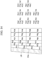
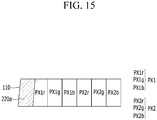
- a first pixel PX1, a second pixel PX2, a third pixel PX3, a fourth pixel PX4, a fifth pixel PX5, a sixth pixel PX6, a seventh pixel PX7, and an eighth pixel PX8 are positioned on the first substrate 110 of the display device according to an exemplary embodiment.
- the pixels PX1, PX2, PX3, PX4, PX5, PX6, PX7, and PX8 respectively include a first subpixel PX1r, PX2r, PX3r, PX4r, PX5r, PX6r, PX7r, and PX8r, a second subpixel PX1g, PX2g, PX3g, PX4g, PX5g, PX6g, PX7g, and PX8g, and a third subpixel PX1b, PX2b, PX3b, PX4b, PX5b, PX6b, PX7b, and PX8b.
- the first pixel PX1 includes the first subpixel PX1r, the second subpixel PX1g, and the third subpixel PX1b
- the second pixel PX2 includes the first subpixel PX2r, the second subpixel PX2g, and the third subpixel PX2b
- the third pixel PX3 includes the first subpixel PX3r, the second subpixel PX3g, and the third subpixel PX3b
- the fourth pixel PX4 includes the first subpixel PX4r, the second subpixel PX4g, and the third subpixel PX4b.
- the fifth pixel PX5 includes the first subpixel PX5r, the second subpixel PX5g, and the third subpixel PX5b;
- the sixth pixel PX6 includes the first subpixel PX6r, the second subpixel PX6g, and the third subpixel PX6b;
- the seventh pixel PX7 includes the first subpixel PX7r, the second subpixel PX7g, and the third subpixel PX7b;
- the eighth pixel PX8 includes the first subpixel PX8r, the second subpixel PX8g, and the third subpixel PX8b.
- Each of the first subpixels PX1r, PX2r, PX3r, PX4r, PX5r, PX6r, PX7r, and PX8r may be subpixels displaying a red colour; each of the second subpixels PX1g, PX2g, PX3g, PX4g, PX5g, PX6g, PX7g, and PX8g may be subpixels displaying a green colour; and each of the third subpixels PX1b, PX2b, PX3b, PX4b, PX5b, PX6b, PX7b, and PX8b may be subpixels displaying a blue colour.
- the subpixels displaying the same colour may be disposed in the same column.
- the arrangement of the subpixels is not limited thereto and may be variously changed.
- each pixel includes the red subpixel, the green subpixel, and the blue subpixel, the present invention is not limited thereto.
- the first colour, the second colour, and the third colour may be any other colours such as primary colours like cyan, magenta, and yellow, instead of red, green, and blue.
- the pixel may further include a white subpixel.
- the first subpixel PX1r, PX2r, PX3r, PX4r, PX5r, PX6r, PX7r, and PX8r; the second subpixel PX1g, PX2g, PX3g, PX4g, PX5g, PX6g, PX7g, and PX8g; and the third subpixel PX1b, PX2b, PX3b, PX4b, PX5b, PX6b, PX7b, and PX8b are disposed in a first direction.
- the first direction may be a row direction.
- the outside light blocking member 220a overlaps the edge of the first substrate 110, and some pixels of the plurality of pixels (PX1, PX2, PX3, PX4, PX5, PX6, PX7, and PX8) overlap the outside light blocking member 220a.
- the first pixel PX1, the third pixel PX3, the fifth pixel PX5 and the seventh pixel PX7 may overlap the outside light blocking member 220a.
- the first subpixel PX1r of the first pixel PX1 may overlap the outside light blocking member 220a.
- the second subpixel PX1g and the third subpixel PX1b of the first pixel do not overlap the outside light blocking member 220a, and the second pixel PX2 adjacent to the first pixel PX1 in the row direction does not overlap the outside light blocking member 220a.
- the second pixel PX2 is disposed farther from the edge of the first substrate 110 than the first pixel PX1.
- the first subpixel PX3r of the third pixel PX3 may overlap the outside light blocking member 220a.
- the second subpixel PX3g and the third subpixel PX3b of the third pixel PX3 do not overlap the outside light blocking member 220a, and the fourth pixel PX4 adjacent to the third pixel PX3 in the row direction does not overlap the outside light blocking member 220a.
- the fourth pixel PX4 is disposed farther from the edge of the first substrate 110 than the third pixel PX3.
- the first subpixel PX5r of the fifth pixel PX5 may overlap the outside light blocking member 220a.
- the second subpixel PX5g and the third subpixel PX5b of the fifth pixel PX5 do not overlap the outside light blocking member 220a, and the sixth pixel PX6 adjacent to the fifth pixel PX5 in the row direction does not overlap the outside light blocking member 220a.
- the sixth pixel PX6 is disposed farther from the edge of the first substrate 110 than the fifth pixel PX5.
- the first subpixel PX7r of the seventh pixel PX7 may overlap the outside light blocking member 220a.
- the second subpixel PX7g and the third subpixel PX7b of the seventh pixel PX7 do not overlap the outside light blocking member 220a, and the eighth pixel PX8 adjacent to the seventh pixel PX7 in the row direction does not overlap the outside light blocking member 220a.
- the eighth pixel PX8 is disposed farther from the edge of the first substrate 110 than the seventh pixel PX7.
- FIG. 3 is a top plan view showing a subpixel of a display device according to an exemplary embodiment
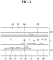
- FIG. 4 is a cross-sectional view taken along the line IV-IV of FIG.3 .
- a display device includes a lower display panel 100 and an upper display panel 200 facing each other, with a liquid crystal layer 3 interposed between the lower display panel 100 and the upper display panel 200.
- a gate line 121 and a gate electrode 124 protruding from the gate line 121 are disposed on the first substrate 110.
- the gate line 121 substantially extends in a horizontal direction and transmits the gate signal.
- the gate electrode 124 protrudes upward from the gate line 121 in plan view.
- the present invention is not limited thereto, and a protruding shape of the gate electrode 124 is modifiable in various ways.
- the gate electrode 124 may not protrude from the gate line 121, but may instead be disposed on the gate line 121.
- a reference voltage line 131 and storage electrodes 135a and 135b protruding from the reference voltage line 131 may be further disposed on the first substrate 110.
- the reference voltage line 131 substantially extends in parallel to the gate line 121, and is separated from the gate line 121. A constant voltage may be applied to the reference voltage line 131.
- the storage electrodes 135a and 135b include a pair of first storage electrodes 135a substantially extending perpendicular to the reference voltage line 131, and a second storage electrode 135b for connecting the pair of first storage electrodes 135a.
- the reference voltage line 131 and the storage electrodes 135a and 135b may surround a pixel electrode 191 that is further described below.
- a gate insulating layer 140 is disposed on the gate line 121, the gate electrode 124, the reference voltage line 131, and the storage electrodes 135a and 135b.
- the gate insulating layer 140 may be made of an inorganic insulating material such as a silicon nitride (SiNx) or a silicon oxide (SiOx).
- the gate insulating layer 140 may also be made of a single layer or multiple layers.
- a semiconductor 154 is disposed on the gate insulating layer 140.
- the semiconductor 154 may be disposed on the gate electrode 124.
- the semiconductor 154 may be made of amorphous silicon, polycrystalline silicon, or a metal oxide.
- An ohmic contact (not shown) may be further disposed on the semiconductor 154.
- the ohmic contact may be made of a material such as a silicide or n+ hydrogenated amorphous silicon doped with an n-type impurity at a high concentration.
- a data line 171, a source electrode 173, and a drain electrode 175 are disposed on the semiconductor 154 and the gate insulating layer 140.
- the data line 171 transmits a data signal and substantially extends in the vertical direction to cross the gate line 121 and the reference voltage line 131.
- the source electrode 173 protrudes over the gate electrode 124 from the data line 171, and it may be bent in a U shape.
- the drain electrode 175 includes a wide end portion and a bar-type end portion. The wide end portion of the drain electrode 175 overlaps the pixel electrode 191. The bar-type end portion of the drain electrode 175 is partially surrounded by the source electrode 173.
- the present invention is not limited thereto, and the source electrode 173 and the drain electrode 175 may have various different shapes.
- the gate electrode 124, the source electrode 173, and the drain electrode 175 collectively form a thin film transistor (TFT) Q along with the semiconductor 154.
- TFT thin film transistor
- a channel of the thin film transistor Q is formed in the semiconductor 154 between the source electrode 173 and the drain electrode 175.
- a passivation layer 180 is disposed on the data line 171, the source electrode 173, and the drain electrode 175.
- the passivation layer 180 is further disposed on a portion of the semiconductor 154 between the source electrode 173 and the drain electrode 175.
- the passivation layer 180 may be made of an organic insulating material or an inorganic insulating material, and it may be made of a single layer or multiple layers.
- a contact hole 181 overlapping at least a portion of the drain electrode 175 is formed in the passivation layer 180.
- the contact hole 181 may expose the wide end portion of the drain electrode 175.
- a pixel electrode 191 is formed on the passivation layer 180.
- the pixel electrode 191 may be made of a transparent conductive material such as an indium-tin oxide (ITO) or an indium-zinc oxide (IZO).
- ITO indium-tin oxide
- IZO indium-zinc oxide
- the pixel electrode 191 is connected to the drain electrode 175 through the contact hole 181. Therefore, when the thin film transistor Q is turned on, the pixel electrode 191 receives a data voltage through the drain electrode 175.
- the pixel electrode 191 has a generally quadrangular shape, and the pixel electrode 191 includes a horizontal stem 193 and a vertical stem 192 crossing each other, with branches 194 extending therefrom, also referred to herein as pixel electrode lines or fine branches.
- the pixel electrode 191 is divided into four sub-regions by the horizontal stem 193 and the vertical stem 192.
- the fine branches 194 extend from the horizontal stem 193 and the vertical stem 192 in an oblique manner, and the extending direction may form an angle of about 45 degrees or 135 degrees with respect to the gate line 121 or the horizontal stem 193.
- the pixel electrode 191 may further include an external stem surrounding the subpixel.
- one subpixel may include a plurality of regions, and a different voltage may be applied to each region.
- a plurality of thin film transistors may be formed in one subpixel.
- a first alignment layer may be formed on an inner surface of the lower display panel 100.
- the first alignment layer may be disposed on the pixel electrode 191.
- a light blocking member 220 is formed on a second substrate 210 made of transparent glass, plastic, or the like.
- the light blocking member 220 is also called a black matrix and prevents light leakage.
- the light blocking member 220 may be formed at a boundary part of each subpixel, such as over the gate line 121, the data line 171, the thin film transistor Q, and the like.
- the light blocking member 220 is formed on the upper panel 200, but the present invention is not limited thereto.
- the light blocking member 220 may be formed in the lower panel 100.
- the outside light blocking member 220a described above may be disposed in the same layer as the light blocking member 220 or may be disposed in another layer. That is, the outside light blocking member 220a may be disposed in the upper panel 200 or may be disposed in the lower panel 100.
- a plurality of colour filters 230 is also formed on the second substrate 210.
- the colour filters 230 may be mainly present in regions enclosed by the light blocking member 220, and may be extended in the vertical direction along a column of the pixel electrodes 191.
- Each of the colour filters 230 may display one of primary colours such as red, green, and blue. Examples of the primary colours may include the three primary colours of red, green, and blue, or yellow, cyan, magenta, and the like.
- a red colour filter may be disposed on the first subpixels PX1r, PX2r, PX3r, PX4r, PX5r, PX6r, PX7r, and PX8r
- a green colour filter may be disposed on the second subpixels PX1g, PX2g, PX3g, PX4g, PX5g, PX6g, PX7g, and PX8g
- a blue colour filter may be disposed on the third subpixels PX1b, PX2b, PX3b, PX4b, PX5b, PX6b, PX7b, and PX8b.
- the colour filters may further include a colour filter displaying a mixed colour of the primary colours or white in addition to the primary colours.
- the colour filter 230 is formed on the upper panel 200, but the present invention is not limited thereto.
- the colour filter 230 may be formed in the lower panel 100.
- An overcoat 240 may be formed on the colour filters 230 and the light blocking member 220.
- the overcoat 240 may be made of an organic insulating material, prevents the colour filters 230 from being exposed, and provides a flat surface.
- the overcoat 240 may also be omitted.
- a common electrode 270 is formed on the overcoat 240.
- the common electrode 270 may be made of a transparent conductive material such as an indium-tin oxide (ITO) or an indium-zinc oxide (IZO).
- ITO indium-tin oxide
- IZO indium-zinc oxide
- a common voltage may be applied to the common electrode 270, and the common voltage may be a predetermined voltage.
- a second alignment layer may be formed on an inner surface of the upper display panel 200.
- the second alignment layer may be disposed on the common electrode 270.
- the liquid crystal layer 3 may include liquid crystal molecules 310 having negative dielectric anisotropy, and the liquid crystal molecules 310 of the liquid crystal layer 3 may be arranged so that long sides thereof are perpendicular to surfaces of the lower display panel 100 and the upper display panel 200 while no electric field is applied.
- the pixel electrode 191 to which a data voltage is applied generates the electric field together with the common electrode 270, to determine the direction of the liquid crystal molecules 310 of the liquid crystal layer 3 disposed between the pixel electrodes 191 and the common electrode 270. Luminance of light passing through the liquid crystal layer 3 becomes different according to the determined direction of the liquid crystal molecules 310.
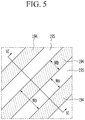
- FIG. 5 is a top plan view showing a portion of a pixel electrode of one subpixel of a display device according to an exemplary embodiment
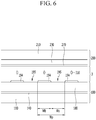
- FIG. 6 is a cross-sectional view taken along the line VI-VI of FIG.5
- FIG. 7 is a top plan view showing a portion of a pixel electrode of another subpixel of a display device according to an exemplary embodiment
- FIG. 8 is a cross-sectional view taken along the line VIII-VIII of FIG. 7 .
- the pixel electrode 191 includes a plurality of branches (fine branches) 194 and slits (fine slits) 195 formed between adjacent fine branches 194.
- the plurality of fine branches 194 is connected to the horizontal stem 193 and the vertical stem 192 so that a data voltage is applied to the plurality of fine branches 194 when the thin film transistor Q is turned on.
- the plurality of fine branches 194 is separated from each other to have a predetermined space.
- Each fine slit 195 is a space between two fine branches 194.
- the width Wb of the fine branch 194 and a space Ws between the fine branches 194 may be constant in one subpixel.
- a pitch Wp of the pixel electrode 191 is defined as a sum of the width Wb of the fine branch 194 and the space Ws between the fine branches 194, and the pitch Wp may also be constant.
- the pixel electrode 191 includes a plurality of fine branches 194 and fine slits 195 disposed between the fine branches 194.
- a width Wb of the fine branches 194, a space Ws between the fine branches 194, and a pitch Wp of the pixel electrode 191 may be constant in one subpixel.
- the width Wb of the fine branches 194 of the subpixel shown in FIG. 7 and FIG. 8 is narrower than the width Wb of the fine branch 194 of the subpixel shown in FIG. 5 and FIG. 6 .
- the space Ws between the fine branches 194 of the subpixel shown in FIG. 7 and FIG. 8 is wider than the space Ws between the fine branches 194 of the subpixel shown in FIG. 5 and FIG. 6 .
- the pitch Wp of the pixel electrode 191 of the subpixel shown in FIG. 7 and FIG. 8 is substantially the same as the pitch Wp of the pixel electrode 191 of the subpixel shown in FIG. 5 and FIG. 6 .
- luminance of the subpixel shown in FIG. 7 and FIG. 8 may be lower than luminance of the subpixel shown in FIG. 5 and FIG. 6 .
- the first subpixel PX1r of the first pixel PX1, and the first subpixel PX2r, the second subpixel PX2g, and the third subpixel PX2b of the second pixel PX2 may have pixel electrode layout shown in FIG. 5 and FIG. 6
- the second subpixel PX1g and the third subpixel PX1b of the first pixel PX1 may have the pixel electrode layout shown in FIG. 7 and FIG. 8 .
- a portion of the first subpixel PX1r overlapping the outside light blocking member 220a is covered by the outside light blocking member 220a so that luminance of that portion becomes lower.
- luminance of the first subpixel PX1r of the first pixel PX1 becomes lower than luminance of the second subpixel PX1g and of the third subpixel PX1b of the first pixel PX1, so that a colour shift is generated.
- a width Wb of the fine branches 194 of the second subpixel PX1g and the third subpixel PX1b of the first pixel PX1 is narrower than a width Wb of the fine branches of the first subpixel PX1r of the first pixel PX1, so that luminance of the second subpixel PX1g and the third subpixel PX1b of the first pixel PX1 may be lower than luminance of the first subpixel PX1r of the first pixel PX1.
- a space Ws between the fine branches 194 of the second subpixel PX1g and third subpixel PX1b of first pixel PX1 may be wider than a space Ws between the fine branches 194 of the first subpixel PX1r of the first pixel PX1.
- a width Wb of the fine branches 194 of the second subpixel PX1g and the third subpixel PX1b of the first pixel PX1 is narrower than a width Wb of the fine branches 194 of the second pixel PX2.
- a space Ws between the fine branches 194 of the second subpixel PX1g and the third subpixel PX1b of the first pixel PX1 may be wider than a space Ws between the fine branches 194 of the second pixel PX2.
- a width Wb of the fine branches 194 of the first subpixel PX1r of the first pixel PX1 is substantially the same as the width Wb of the fine branches 194 of the second pixel PX2.
- a space Ws between the fine branches 194 of the first subpixel PX1r of the first pixel PX1 is substantially the same as a space Ws between the fine branches 194 of the second pixel PX2.
- a pitch Wp of the pixel electrode 191 of the first pixel PX1 and a pitch Wp of the pixel electrode 191 of the second pixel PX2 are substantially the same.
- the first subpixel PX3r of the third pixel PX3 overlaps the outside light blocking member 220a, so that luminance of the first subpixel PX3r of the third pixel PX3 becomes lower.
- a width Wb of the fine branches 194 of the second subpixel PX3g and third subpixel PX3b of the third pixel PX3 it is possible to prevent colour shift from being generated in the third pixel PX3.
- a width Wb of the fine branches 194 of the second subpixel PX3g and the third subpixel PX3b of the third pixel PX3 is narrower than a width Wb of the fine branches 194 of the first subpixel PX3r of the third pixel PX3 and the fourth pixel PX4.
- a space Ws between the fine branches 194 of the second subpixel PX3g and the third subpixel PX3b of the third pixel PX3 may be wider than a space Ws between the fine branches 194 of the first subpixel PX3r of the third pixel PX3 and the fourth pixel PX4.
- An area of overlap between the first subpixel PX3r of the third pixel PX3 and the outside light blocking member 220a is smaller than an area of overlap between the first subpixel PX1r of the first pixel PX1 and the outside light blocking member 220a.
- a decrement of luminance of the first subpixel PX3r of the third pixel PX3 is lower than a decrement of luminance of the first subpixel PX1r of the first pixel PX1.
- a width Wb of the fine branches 194 of the second subpixel PX3g and the third subpixel PX3b of the third pixel PX3 may be wider than a width Wb of the fine branches 194 of the second subpixel PX1g and the third subpixel PX1b of the first pixel PX1. That is, a width Wb of the fine branch 194 may be controlled by considering a decrement of luminance according to an area of overlap between the corresponding subpixel and the outside light blocking member 220a.
- the first subpixel PX5r of the fifth pixel PX5 overlaps the outside light blocking member 220a, so that luminance of the first subpixel PX5r of the fifth pixel PX5 becomes lower.
- a width Wb of the fine branches 194 of the second subpixel PX5g and the third subpixel PX5b of the fifth pixel PX5 it is possible to prevent colour shift from being generated in the fifth pixel PX5.
- a width Wb of the fine branches 194 of the second subpixel PX5g and the third subpixel PX5b of the fifth pixel PX5 is narrower than a width Wb of the fine branches 194 of the first subpixel PX5r of the fifth pixel PX5 and the sixth pixel PX6.
- a space Ws between the fine branches 194 of the second subpixel PX5g and the third subpixel PX5b of the fifth pixel PX5 may be wider than a space Ws between the fine branches 194 of the first subpixel PX5r of the fifth pixel PX5 and the sixth pixel PX6.
- An area of overlap between the first subpixel PX5r of the fifth pixel PX5 and the outside light blocking member 220a is smaller than an area of overlap between the first subpixel PX3r of the third pixel PX3 and the outside light blocking member 220a.
- a decrement of luminance of the first subpixel PX5r of the fifth pixel PX5 is lower than a decrement of luminance of the first subpixel PX3r of the third pixel PX3.
- a width Wb of the fine branches 194 of the second subpixel PX5g and the third subpixel PX5b of the fifth pixel PX5 may be wider than a width Wb of the fine branches 194 of the second subpixel PX3g and the third subpixel PX3b of the third pixel PX3. That is, a width Wb of the fine branches 194 may be controlled by considering a decrement of luminance according to an area of overlap between the corresponding subpixel and the outside light blocking member 220a.
- the first subpixel PX7r of the seventh pixel PX7 overlaps the outside light blocking member 220a so that luminance of the first subpixel PX7r of the seventh pixel PX7 becomes lower.
- a width Wb of the fine branches 194 of the second subpixel PX7g and the third subpixel PX7b of the seventh pixel PX7 it is possible to prevent the colour shift from being generated in the seventh pixel PX7.
- a width Wb of the fine branches 194 of the second subpixel PX7g and the third subpixel PX7b of the seventh pixel PX7 is narrower than a width Wb of the fine branches 194 of the first subpixel PX7r of the seventh pixel PX7 and the eighth pixel PX8.
- a space Ws between the fine branches 194 of the second subpixel PX7g and the third subpixel PX7b of the seventh pixel PX7 may be wider than a space Ws between the fine branches 194 of the first subpixel PX7r of the seventh pixel PX7 and the eighth pixel PX8.
- An area of overlap between the first subpixel PX7r of the seventh pixel PX7 and the outside light blocking member 220a is smaller than an area of overlap between the first subpixel PX5r of the fifth pixel PX5 and the outside light blocking member 220a.
- a decrement of luminance of the first subpixel PX7r of the seventh pixel PX7 is lower than a decrement of luminance of the first subpixel PX5r of the fifth pixel PX5.
- a width Wb of the fine branches 194 of the second subpixel PX7g and the third subpixel PX7b of the seventh pixel PX7 may be wider than a width Wb of the fine branches 194 of the second subpixel PX5g and the third subpixel PX5b of the fifth pixel PX5. That is, a width Wb of the fine branches 194 may be controlled by considering a decrement of luminance according to an area of overlap between the corresponding subpixel and the outside light blocking member 220a.
- the present exemplary embodiment is similar to the display device according to the exemplary embodiment shown in FIG. 1 to FIG. 8 such that redundant description thereof is omitted.
- a decrement of the luminance of the subpixel may be compensated differently from the previous exemplary embodiment, and this will be described in detail.
- FIG. 9 is a top plan view showing a portion of a pixel electrode of a subpixel of a display device according to an exemplary embodiment
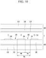
- FIG. 10 is a cross-sectional view taken along the line X-X of FIG.9 .
- the pixel electrode 191 includes a plurality of fine branches 194 and a fine slit 195 disposed between the plurality of fine branches 194.
- the width Wb of each fine branch 194, the space Ws between the fine branches 194, and the pitch Wp of the pixel electrode 191 may be constant in one subpixel.
- the width Wb of the fine branches 194 of the subpixel shown in FIG. 9 and FIG. 10 is greater than the width Wb of the fine branches 194 of the subpixel shown in FIG. 5 and
- the space Ws between the fine branches 194 of the subpixel shown in FIG. 9 and FIG. 10 is narrower than the space Ws between the fine branches 194 of the subpixel shown in FIG. 5 and FIG. 6 .
- the pitch Wp of the pixel electrode 191 of the subpixel shown in FIG. 9 and FIG. 10 is substantially the same as the pitch Wp of the pixel electrode 191 of the subpixel shown in FIG. 5 and FIG. 6 .
- luminance of the subpixel shown in FIG. 9 and FIG. 10 may be greater than luminance of the subpixel shown in FIG. 5 and FIG. 6 .
- the second subpixel PX1g and the third subpixel PX1b of the first pixel PX1, and the first subpixel PX2r, the second subpixel PX2g, and the third subpixel PX2b of the second pixel PX2 may have a shape of a subpixel shown in FIG. 5 and FIG. 6
- the first subpixel PX1r of the first pixel PX1 may have a shape of a subpixel shown in FIG. 9 and FIG. 10 .
- a portion of the first subpixel PX1r of the first pixel PX1 overlapping the outside light blocking member 220a is covered by the outside light blocking member 220a, so that luminance of the portion becomes lower.
- luminance of the first subpixel PX1r of the first pixel PX1 becomes lower than luminance of the second subpixel PX1g and the third subpixel PX1b of the first pixel PX1, so that a colour shift is generated.
- a width Wb of the fine branches 194 of the first subpixel PX1r of the first pixel PX1 is wider than a width Wb of the fine branches of the second subpixel PX1g and the third subpixel PX1b of the first pixel PX1, so that luminance of the first subpixel PX1r of the first pixel PX1 becomes higher than luminance of the second subpixel PX1g and the third subpixel PX1b of the first pixel PX1.
- luminance of the first pixel PX1 overlapping the outside light blocking member 220a may be maintained at a level similar to luminance of the second pixel PX2, thus the rounded edge of the display device may be prevented from being represented as a step shape.
- a space Ws between the fine branches 194 of the first subpixel PX1r of first pixel PX1 may be narrower than a space Ws between the fine branches 194 of the second subpixel PX1g and third subpixel PX1b of the first pixel PX1.
- a width Wb of the fine branches 194 of the first subpixel PX1r of the first pixel PX1 is wider than a width Wb of the fine branches 194 of the second pixel PX2.
- a space Ws between the fine branches 194 of the first subpixel PX1r of the first pixel PX1 may be narrower than a space Ws between the fine branches 194 of the second pixel PX2.
- a width Wb of the fine branches 194 of the second subpixel PX1g and the third subpixel PX1b of the first pixel PX1 is substantially the same as the width Wb of the fine branches 194 of the second pixel PX2.
- a space Ws between the fine branches 194 of the second subpixel PX1g and the third subpixel PX1b of the first pixel PX1 is substantially the same as a space Ws between the fine branches 194 of the second pixel PX2.
- a pitch Wp of the pixel electrode 191 of the first pixel PX1 and a pitch Wp of the pixel electrode 191 of the second pixel PX2 are substantially the same.
- the first subpixel PX3r of the third pixel PX3 overlaps the outside light blocking member 220a, so that luminance of the first subpixel PX3r of the third pixel PX3 becomes lower.
- a width Wb of the fine branches 194 of the first subpixel PX3r of the third pixel PX3 is wider than a width Wb of the fine branches 194 of the second subpixel PX3g and the third subpixel PX3b of the third pixel PX3 and the fourth pixel PX4.
- a space Ws between the fine branches 194 of the first subpixel PX3r of the third pixel PX3 may be narrower than a space Ws between the fine branches 194 of the second subpixel PX3g and the third subpixel PX3b of the third pixel PX3 and the fourth pixel PX4.
- An area of overlap between the first subpixel PX3r of the third pixel PX3 and the outside light blocking member 220a is smaller than an area of overlap between the first subpixel PX1r of the first pixel PX1 and the outside light blocking member 220a.
- a decrement of luminance of the first subpixel PX3r of the third pixel PX3 is lower than a decrement of luminance of the first subpixel PX1r of the first pixel PX1.
- a width Wb of the fine branches 194 of the first subpixel PX3r of the third pixel PX3 may be narrower than a width Wb of the fine branches 194 of the first subpixel PX1r of the first pixel PX1. That is, a width Wb of the fine branches 194 may be controlled by considering a decrement of luminance according to an area of overlap between the corresponding subpixel and the outside light blocking member 220a.
- the first subpixel PX5r of the fifth pixel PX5 overlaps the outside light blocking member 220a, so that luminance of the first subpixel PX5r of the fifth pixel PX5 becomes lower.
- a width Wb of the fine branches 194 of the first subpixel PX5r of the fifth pixel PX5 is wider than a width Wb of the fine branches 194 of the second subpixel PX5g and the third subpixel PX5b of the fifth pixel PX5 and the sixth pixel PX6.
- a space Ws between the fine branches 194 of the first subpixel PX5r of the fifth pixel PX5 may be narrower than a space Ws between the fine branches 194 of the second subpixel PX5g and the third subpixel PX5b of the fifth pixel PX5 and the sixth pixel PX6.
- An area of overlap between the first subpixel PX5r of the fifth pixel PX5 and the outside light blocking member 220a is smaller than an area of overlap between the first subpixel PX3r of the third pixel PX3 and the outside light blocking member 220a.
- a decrement of luminance of the first subpixel PX5r of the fifth pixel PX5 is lower than a decrement of luminance of the first subpixel PX3r of the third pixel PX3.
- a width Wb of the fine branches 194 of the first subpixel PX5r of the fifth pixel PX5 may be narrower than a width Wb of the fine branches 194 of the first subpixel PX3r of the third pixel PX3. That is, a width Wb of the fine branches 194 may be controlled by considering a decrement of luminance according to an overlapping area of the corresponding subpixel and the outside light blocking member 220a.
- the first subpixel PX7r of the seventh pixel PX7 overlaps the outside light blocking member 220a, so that luminance of the first subpixel PX7r of the seventh pixel PX7 becomes lower.
- a width Wb of the fine branches 194 of the first subpixel PX7r of the seventh pixel PX7 it is possible to prevent the colour shift from being generated in the seventh pixel PX7.
- a width Wb of the fine branches 194 of the first subpixel PX7r of the seventh pixel PX7 is wider than a width Wb of the fine branches 194 of the second subpixel PX7g and the third subpixel PX7b of the seventh pixel PX7 and the eighth pixel PX8.
- a space Ws between the fine branches 194 of the first subpixel PX7r of the seventh pixel PX7 may be narrower than a space Ws between the fine branches 194 of the second subpixel PX7g and the third subpixel PX7b of the seventh pixel PX7 and the eighth pixel PX8.
- An area of overlap between the first subpixel PX7r of the seventh pixel PX7 and the outside light blocking member 220a is smaller than an area of overlap between the first subpixel PX5r of the fifth pixel PX5 and the outside light blocking member 220a.
- a decrement of luminance of the first subpixel PX7r of the seventh pixel PX7 is lower than a decrement of luminance of the first subpixel PX5r of the fifth pixel PX5.
- a width Wb of the fine branches 194 of the first subpixel PX7r of the seventh pixel PX7 may be narrower than a width Wb of the fine branches 194 of the first subpixel PX5r of the fifth pixel PX5. That is, a width Wb of the fine branches 194 may be controlled by considering a decrement of luminance according to an overlapping area of the corresponding subpixel and the outside light blocking member 220a.
- the present exemplary embodiment is similar to the display device according to the exemplary embodiment shown in FIG. 1 to FIG. 8 such that redundant description thereof is omitted.
- luminance of the corresponding subpixel may be controlled differently from the previous exemplary embodiment, as will be described in further detail below.
- FIG. 11 is a top plan view showing a portion of a pixel electrode of one subpixel of a display device according to an exemplary embodiment
- FIG. 12 is a top plan view showing a portion of a pixel electrode of another subpixel of a display device according to an exemplary embodiment.
- the pixel electrode 191 includes a horizontal stem 193, a vertical stem 192, and a plurality of fine branches 194 extending therefrom.
- a fine slit 195 is formed between pairs of fine branches 194.
- the fine branches 194 are inclined with respect to the horizontal stem 193, to form a predetermined angle between the fine branches 194 and the horizontal stem 193.
- An angle ⁇ between the horizontal stem 193 and the fine branches 194 in FIG. 12 is smaller than an angle ⁇ between the horizontal stem 193 and the fine branches 194 in FIG. 11 .
- an angle ⁇ between the horizontal stem 193 and the fine branches 194 in FIG. 11 may be about 40 degrees
- an angle ⁇ between the horizontal stem 193 and the fine branches 194 in FIG. 12 may be about 35 degrees.
- luminance of a subpixel shown in FIG. 12 may be lower than luminance of a subpixel shown in FIG. 11 .
- the first subpixel PX1r of the first pixel PX1, and the first subpixel PX2r, the second subpixel PX2g, and the third subpixel PX2b of the second pixel PX2 may have a shape of a subpixel shown in FIG. 11
- the second subpixel PX1g and the third subpixel PX1b of the first pixel PX1 may have a shape of a subpixel shown in FIG. 12 .
- a portion of the first subpixel PX1r of the first pixel PX1 is covered by the outside light blocking member 220a, so that luminance of that portion becomes lower.
- luminance of the first subpixel PX1r of the first pixel PX1 becomes lower than luminance of the second subpixel PX1g and the third subpixel PX1b of the first pixel PX1, so that a colour shift is generated.
- an angle ⁇ between the horizontal stem 193 and the fine branches 194 disposed in the second subpixel PX1g and the third subpixel PX1b of the first pixel PX1 is smaller than an angle ⁇ between the horizontal stem 193 and the fine branches 194 disposed in the first subpixel PX1r of the first pixel PX1, so that luminance of the second subpixel PX1g and the third subpixel PX1b of the first pixel PX1 may become lower than luminance of the first subpixel PX1r of the first pixel PX1.
- an angle ⁇ between the horizontal stem 193 and the fine branches 194 disposed in the second subpixel PX1g and the third subpixel PX1b of the first pixel PX1 is smaller than an angle ⁇ between the horizontal stem 193 and the fine branches 194 disposed in the second pixel PX2.
- An angle ⁇ between the horizontal stem 193 and the fine branches 194 disposed in the first subpixel PX1r of the first pixel PX1 may be substantially the same as an angle ⁇ between the horizontal stem 193 and the fine branches 194 disposed in the second pixel PX2.
- the first subpixel PX3r of the third pixel PX3 overlaps the outside light blocking member 220a, so that luminance of the first subpixel PX3r of the third pixel PX3 becomes lower.
- an angle ⁇ between the horizontal stem 193 and the fine branches 194 disposed in the second subpixel PX3g and the third subpixel PX3b of the third pixel PX3 is smaller than an angle ⁇ between the horizontal stem 193 and the fine branches 194 disposed in the first subpixel PX3r of the third pixel PX3 and the fourth pixel PX4.
- An area of overlap between the first subpixel PX3r of the third pixel PX3 and the outside light blocking member 220a is smaller than an area of overlap between the first subpixel PX1r of the first pixel PX1 and the outside light blocking member 220a.
- a decrement of luminance of the first subpixel PX3r of the third pixel PX3 is lower than a decrement of luminance of the first subpixel PX1r of the first pixel PX1.
- an angle ⁇ between the horizontal stem 193 and the fine branches 194 disposed in the second subpixel PX3g and the third subpixel PX3b of the third pixel PX3 may be greater than an angle ⁇ between the horizontal stem 193 and the fine branches 194 disposed in the second subpixel PX1g and the third subpixel PX1b of the first pixel PX1. That is, an angle ⁇ between the horizontal stem 193 and the fine branches 194 may be controlled by considering a decrement of luminance according to an area of overlap between the corresponding subpixel and the outside light blocking member 220a.
- the first subpixel PX5r of the fifth pixel PX5 overlaps the outside light blocking member 220a, so that luminance of the first subpixel PX5r of the fifth pixel PX5 becomes lower.
- an angle ⁇ between the horizontal stem 193 and the fine branches 194 disposed in the second subpixel PX5g and the third subpixel PX5b of the fifth pixel PX5 is smaller than an angle ⁇ between the horizontal stem 193 and the fine branches 194 disposed in the first subpixel PX5r of the fifth pixel PX5 and the sixth pixel PX6.
- An area of overlap between the first subpixel PX5r of the fifth pixel PX5 and the outside light blocking member 220a is smaller than an area of overlap between the first subpixel PX3r of the third pixel PX3 and the outside light blocking member 220a.
- a decrement of luminance of the first subpixel PX5r of the fifth pixel PX5 is lower than a decrement of luminance of the first subpixel PX3r of the third pixel PX3.
- an angle ⁇ between the horizontal stem 193 and the fine branches 194 disposed in the second subpixel PX5g and the third subpixel PX5b of the fifth pixel PX5 may be greater than an angle ⁇ between the horizontal stem 193 and the fine branches 194 disposed in the second subpixel PX3g and the third subpixel PX3b of the third pixel PX3. That is, an angle ⁇ between the horizontal stem 193 and the fine branches 194 may be controlled by considering a decrement of luminance according to an area of overlap between the corresponding subpixel and the outside light blocking member 220a.
- the first subpixel PX7r of the seventh pixel PX7 overlaps the outside light blocking member 220a, so that luminance of the first subpixel PX7r of the seventh pixel PX7 becomes lower.
- an angle ⁇ between the horizontal stem 193 and the fine branches 194 disposed in the second subpixel PX7g and the third subpixel PX7b of the seventh pixel PX7 is smaller than an angle ⁇ between the horizontal stem 193 and the fine branches 194 disposed in the first subpixel PX7r of the seventh pixel PX7 and the eighth pixel PX8.
- An area of overlap between the first subpixel PX7r of the seventh pixel PX7 and the outside light blocking member 220a is smaller than an area of overlap between the first subpixel PX5r of the fifth pixel PX5 and the outside light blocking member 220a.
- a decrement of luminance of the first subpixel PX7r of the seventh pixel PX7 is lower than a decrement of luminance of the first subpixel PX5r of the fifth pixel PX5.
- an angle ⁇ between the horizontal stem 193 and the fine branches 194 disposed in the second subpixel PX7g and the third subpixel PX7b of the seventh pixel PX7 may be greater than an angle ⁇ between the horizontal stem 193 and the fine branches 194 disposed in the second subpixel PX5g and the third subpixel PX5b of the fifth pixel PX5. That is, an angle ⁇ between the horizontal stem 193 and the fine branches 194 may be controlled by considering a decrement of luminance according to an area of overlap between the corresponding subpixel and the outside light blocking member 220a.
- the present exemplary embodiment is similar to the display device according to the exemplary embodiment shown in FIG. 11 and FIG. 12 such that redundant description thereof is omitted.
- a decrement of the luminance of the subpixel may be compensated differently from the previous exemplary embodiment, and this will be described in further detail below.
- FIG. 13 is a top plan view showing a portion of a pixel electrode of a subpixel of a display device according to an exemplary embodiment.
- the pixel electrode 191 includes a horizontal stem 193, a vertical stem 192, and a plurality of fine branches 194 extending therefrom. Fine slits 195 are formed between adjacent fine branches 194.
- the fine branches 194 are inclined with respect to the horizontal stem 193 to, form a predetermined angle ⁇ between the fine branches 194 and the horizontal stem 193.
- An angle ⁇ between the horizontal stem 193 and the fine branches 194 in FIG. 13 is greater than an angle ⁇ between the horizontal stem 193 and the fine branches 194 in FIG. 11 .
- an angle ⁇ between the horizontal stem 193 and the fine branches 194 in FIG. 11 may be about 40 degrees
- an angle ⁇ between the horizontal stem 193 and the fine branches 194 in FIG. 13 may be about 45 degrees.
- luminance of a subpixel shown in FIG. 13 may be higher than luminance of a subpixel shown in FIG. 11 .
- the second subpixel PX1g and third subpixel PX1b of the first pixel PX1, and the first subpixel PX2r, the second subpixel PX2g, and the third subpixel PX2b of the second pixel PX2 may have a shape of a subpixel shown in FIG. 11
- the first subpixel PX1r of the first pixel PX1 may have a shape of a subpixel shown in FIG. 13 .
- a portion of the first subpixel PX1r of the first pixel PX1 is covered by the outside light blocking member 220a, so that luminance of the portion becomes lower.
- luminance of the first subpixel PX1r of the first pixel PX1 becomes lower than luminance of the second subpixel PX1g and the third subpixel PX1b of the first pixel PX1, so that a colour shift is generated.
- an angle ⁇ between the horizontal stem 193 and the fine branches 194 disposed in the first subpixel PX1r of the first pixel PX1 is greater than an angle ⁇ between the horizontal stem 193 and the fine branches 194 disposed in the second subpixel PX1g and the third subpixel PX1b of the first pixel PX1, so that luminance of the first subpixel PX1r of the first pixel PX1 may be greater than luminance of the second subpixel PX1g and the third subpixel PX1b of the first pixel PX1.
- luminance of the first pixel PX1 overlapping the outside light blocking member 220a may be maintained at a level similar to luminance of the second pixel PX2, thus the rounded edge of the display device may be prevented from being represented as a step shape.
- an angle ⁇ between the horizontal stem 193 and the fine branches 194 disposed in the first subpixel PX1r of the first pixel PX1 is larger than an angle ⁇ between the horizontal stem 193 and the fine branches 194 disposed in the second pixel PX2.
- An angle ⁇ between the horizontal stem 193 and the fine branches 194 disposed in the second subpixel PX1g and the third subpixel PX1b of the first pixel PX1 may be substantially the same as an angle ⁇ between the horizontal stem 193 and the fine branches 194 disposed in the second pixel PX2.
- the first subpixel PX3r of the third pixel PX3 overlaps the outside light blocking member 220a, so that luminance of the first subpixel PX3r of the third pixel PX3 becomes lower.
- an angle ⁇ between the horizontal stem 193 and the fine branches 194 disposed in the first subpixel PX3r of the third pixel PX3 is greater than an angle ⁇ between the horizontal stem 193 and the fine branches 194 disposed in the second and third subpixels PX3g and PX3b of the third pixel PX3 and the fourth pixel PX4.
- An area of overlap between the first subpixel PX3r of the third pixel PX3 and the outside light blocking member 220a is smaller than an area of overlap between the first subpixel PX1r of the first pixel PX1 and the outside light blocking member 220a.
- a decrement of luminance of the first subpixel PX3r of the third pixel PX3 is lower than a decrement of luminance of the first subpixel PX1r of the first pixel PX1.
- an angle ⁇ between the horizontal stem 193 and the fine branches 194 disposed in the first subpixel PX3r of the third pixel PX3 may be smaller than an angle ⁇ between the horizontal stem 193 and the fine branches 194 disposed in the first subpixel PX1r of the first pixel PX1. That is, an angle ⁇ between the horizontal stem 193 and the fine branches 194 may be controlled by considering a decrement of luminance according to an overlapping area of the corresponding subpixel and the outside light blocking member 220a.
- the first subpixel PX5r of the fifth pixel PX5 overlaps the outside light blocking member 220a, so that luminance of the first subpixel PX5r of the fifth pixel PX5 becomes lower.
- an angle ⁇ between the horizontal stem 193 and the fine branches 194 disposed in the first subpixel PX5r of the fifth pixel PX5 is greater than an angle ⁇ between the horizontal stem 193 and the fine branches 194 disposed in the second subpixel PX5g and the third subpixel PX5b of the fifth pixel PX5 and the sixth pixel PX6.
- An area of overlap between the first subpixel PX5r of the fifth pixel PX5 and the outside light blocking member 220a is smaller than an area of overlap between the first subpixel PX3r of the third pixel PX3 and the outside light blocking member 220a.
- a decrement of luminance of the first subpixel PX5r of the fifth pixel PX5 is lower than a decrement of luminance of the first subpixel PX3r of the third pixel PX3.
- an angle ⁇ between the horizontal stem 193 and the fine branches 194 disposed in the first subpixel PX5r of the fifth pixel PX5 may be smaller than an angle ⁇ between the horizontal stem 193 and the fine branches 194 disposed in the first subpixel PX3r of the third pixel PX3. That is, an angle ⁇ between the horizontal stem 193 and the fine branches 194 may be controlled by considering a decrement of luminance according to an area of overlap between the corresponding subpixel and the outside light blocking member 220a.
- the first subpixel PX7r of the seventh pixel PX7 overlaps the outside light blocking member 220a, so that luminance of the first subpixel PX7r of the seventh pixel PX7 becomes lower.
- an angle ⁇ between the horizontal stem 193 and the fine branches 194 disposed in the first subpixel PX7r of the seventh pixel PX7 is greater than an angle ⁇ between the horizontal stem 193 and the fine branches 194 disposed in the second subpixel PX7g and the third subpixel PX7b of the seventh pixel PX7 and the eighth pixel PX8.
- An area of overlap between the first subpixel PX7r of the seventh pixel PX7 and the outside light blocking member 220a is smaller than an area of overlap between the first subpixel PX5r of the fifth pixel PX5 and the outside light blocking member 220a.
- a decrement of luminance of the first subpixel PX7r of the seventh pixel PX7 is lower than a decrement of luminance of the first subpixel PX5r of the fifth pixel PX5.
- an angle ⁇ between the horizontal stem 193 and the fine branches 194 disposed in the first subpixel PX7r of the seventh pixel PX7 may be smaller than an angle ⁇ between the horizontal stem 193 and the fine branches 194 disposed in the first subpixel PX5r of the fifth pixel PX5. That is, an angle ⁇ between the horizontal stem 193 and the fine branches 194 may be controlled by considering a decrement of luminance according to an overlapping area of the corresponding subpixel and the outside light blocking member 220a.
- FIG. 14 is a top plan view showing a portion of pixels of a display device according to an exemplary embodiment.
- FIG. 14 shows pixels disposed on a rounded edge and pixels adjacent thereto.
- a first pixel PX1, a second pixel PX2, a third pixel PX3, a fourth pixel PX4, a fifth pixel PX5, a sixth pixel PX6, a seventh pixel PX7, and an eighth pixel PX8 are positioned on the first substrate 110 of the display device according to an exemplary embodiment.
- the outside light blocking member 220a overlaps the edge of the first substrate 110, and some pixels of the plurality of pixels PX1, PX2, PX3, PX4, PX5, PX6, PX7, and PX8 may be adjacent to the outside light blocking member 220a.
- the first pixel PX1, the third pixel PX3, the fifth pixel PX5 and the seventh pixel PX7 may be adjacent to the outside light blocking member 220a.
- the second pixel PX2 is disposed farther from the edge of the first substrate 110 than the first pixel PX1
- the fourth pixel PX4 is disposed farther from the edge of the first substrate 110 than the third pixel PX3.
- the sixth pixel PX6 is disposed farther from the edge of the first substrate 110 than the fifth pixel PX5
- the eighth pixel PX8 is disposed farther from the edge of the first substrate 110 than the seventh pixel PX7.
- a size of the first pixel PX1 is smaller than a size of the second pixel PX2.
- the first subpixel PX1r, the second subpixel PX1g, and third subpixel PX1b of the first pixel PX1 are substantially the same size.
- a shape of the first subpixel PX1r, a shape of the second subpixel PX1g, and a shape of the third subpixel PX1b of the first pixel PX1 in a plan view may be different from each other.
- a shape of the second subpixel PX1g and a shape of the third subpixel PX1b in a plan view may be approximately rectangular.
- a shape of the first subpixel PX1r of the first pixel PX1 in a plan view may be approximately trapezoidal.
- a shape of the first subpixel PX1r of the first pixel PX1 in a plan view may also be a figure including three straight lines and a curved line.
- a length of a lower edge of the first subpixel PX1r of the first pixel PX1 may be longer than a length of a lower edge of the second subpixel PX1g of the first pixel PX1. Also, a length of an upper edge of the first subpixel PX1r of the first pixel PX1 is shorter than a length of an upper edge of the second subpixel PX1g of the first pixel PX1.
- the exemplary embodiment is not limited thereto, and a shape of the first subpixel PX1r may be variously changed according to a shape of the outside light blocking member 220a.
- the length of the upper edge of the first subpixel PX1r of the first pixel PX1 may be longer than the length of the upper edge of the second subpixel PX1g of the first pixel PX1.
- the length of the lower edge of the first subpixel PX1r of the first pixel PX1 is shorter than the length of the lower edge of the second subpixel PX1g of the first pixel PX1.
- a shape of the first subpixel PX1r, a shape of the second subpixel PX1g, and a shape of the third subpixel PX1b of the first pixel PX1 are different from each other, a size of the first subpixel PX1r, a size of the second subpixel PX1g, and a size of the third subpixel PX1b of the first pixel PX1 are substantially the same, thus it is possible to prevent colour shift from being generated in the first pixel PX1.
- Luminance of the first pixel PX1 may be lower than luminance of the second pixel PX2.
- a width Wb of the fine branches 194 disposed in the first pixel PX1 is wider than a width Wb of the fine branches 194 disposed in the second pixel PX2, so that any decrease in luminance of the subpixel may be compensated. That is, luminance of the first pixel PX1 and luminance of the second pixel PX2 may become substantially the same.
- a space Ws between the fine branches 194 disposed in the first pixel PX1 may be narrower than a space Ws between the fine branches 194 disposed in the second pixel PX2.
- a pitch Wp of the pixel electrode 191 disposed in the first pixel PX1 may be substantially the same as a pitch Wp of the pixel electrode 191 disposed in the second pixel PX2.
- the present invention by controlling a width Wb of the fine branches 194 disposed in the first pixel PX1, reduction in luminance of the subpixel may be compensated.
- the present invention is not limited thereto.
- a decrement of the luminance of the subpixel may be compensated.
- a size of the third pixel PX3 is smaller than a size of the fourth pixel PX4.
- a size of the first subpixel PX3r, a size of the second subpixel PX3g, and a size of the third subpixel PX3b of the third pixel PX3 are substantially the same.
- a shape of the first subpixel PX3r, a shape of the second subpixel PX3g, and a shape of the third subpixel PX3b of the third pixel PX3 in a plan view may be different from each other.
- a shape of the first subpixel PX3r, a shape of the second subpixel PX3g, and a shape of the third subpixel PX3b of the third pixel PX3 are different from each other, a size of the first subpixel PX3r, a size of the second subpixel PX3g, and a size of the third subpixel PX3b of the third pixel PX3 are substantially the same, thus it is possible to prevent colour shift from being generated in the third pixel PX3.
- Luminance of the third pixel PX3 may be lower than luminance of the fourth pixel PX4.
- a width Wb of the fine branches 194 disposed in the third pixel PX3 that is wider than a width Wb of the fine branches 194 disposed in the fourth pixel PX4
- a decrement of the luminance of the subpixel may be compensated.
- a size of the third pixel PX3 is larger than a size of the first pixel PX1.
- luminance of the third pixel PX3 is higher than luminance of the first pixel PX1.
- a width Wb of the fine branches 194 disposed in the third pixel PX3 may be narrower than a width Wb of the fine branches 194 disposed in the first pixel PX1.
- an angle ⁇ between the horizontal stem 193 and the fine branches 194 disposed in the third pixel PX3 that is greater than an angle ⁇ between the horizontal stem 193 and the fine branches 194 disposed in the fourth pixel PX4
- a decrement of the luminance of the subpixel may be compensated.
- an angle ⁇ between the horizontal stem 193 and the fine branches 194 disposed in the third pixel PX3 may be smaller than an angle ⁇ between the horizontal stem 193 and the fine branches 194 disposed in the first pixel PX1.
- a size of the fifth pixel PX5 is smaller than a size of the sixth pixel PX6.
- a size of the first subpixel PX5r, a size of the second subpixel PX5g, and a size of the third subpixel PX5b of the fifth pixel PX5 are substantially the same.
- a shape of the first subpixel PX5r, a shape of the second subpixel PX5g, and a shape of the third subpixel PX5b of the fifth pixel PX5 in a plan view may be different from each other.
- a shape of the first subpixel PX5r, a shape of the second subpixel PX5g, and a shape of the third subpixel PX5b of the fifth pixel PX5 are different from each other, a size of the first subpixel PX5r, a size of the second subpixel PX5g, and a size of the third subpixel PX5b of the fifth pixel PX5 are substantially the same.
- Luminance of the fifth pixel PX5 may be lower than luminance of the sixth pixel PX6.
- a width Wb of the fine branches 194 disposed in the fifth pixel PX5 that is wider than a width Wb of the fine branches 194 disposed in the sixth pixel PX6, a decrement of the luminance of the subpixel may be compensated.
- a size of the fifth pixel PX5 is larger than a size of the third pixel PX3.
- luminance of the fifth pixel PX5 is higher than luminance of the third pixel PX3.
- a width Wb of the fine branch 194 disposed in the fifth pixel PX5 may be narrower than a width Wb of the fine branch 194 disposed in the third pixel PX3.
- an angle ⁇ between the horizontal stem 193 and the fine branches 194 disposed in the fifth pixel PX5 that is greater than an angle ⁇ between the horizontal stem 193 and the fine branches 194 disposed in the sixth pixel PX6, a decrement of the luminance of the subpixel may be compensated.
- an angle ⁇ between the horizontal stem 193 and the fine branches 194 disposed in the fifth pixel PX5 may be smaller than an angle ⁇ between the horizontal stem 193 and the fine branches 194 disposed in the third pixel PX3.
- a size of the seventh pixel PX7 is smaller than a size of the eighth pixel PX8.
- a size of the first subpixel PX7r, a size of the second subpixel PX7g, and a size of the third subpixel PX7b of the seventh pixel PX7 are substantially the same.
- a shape of the first subpixel PX7r, a shape of the second subpixel PX7g, and a shape of the third subpixel PX7b of the seventh pixel PX7 in a plan view may be different from each other.
- a shape of the first subpixel PX7r, a shape of the second subpixel PX7g, and a shape of the third subpixel PX7b of the seventh pixel PX7 are different from each other, a size of the first subpixel PX7r, a size of the second subpixel PX7g, and a size of the third subpixel PX7b of the seventh pixel PX7 are substantially the same. Thus, it is possible to prevent colour shift from being generated in the seventh pixel PX7.
- Luminance of the seventh pixel PX7 may be lower than luminance of the eighth pixel PX8.
- a decrement of the luminance of the subpixel may be compensated.
- a size of the seventh pixel PX7 is larger than a size of the fifth pixel PX5.
- luminance of the seventh pixel PX7 is higher than luminance of the fifth pixel PX5.
- a width Wb of the fine branches 194 disposed in the seventh pixel PX7 may be narrower than a width Wb of the fine branches 194 disposed in the fifth pixel PX5.
- an angle ⁇ between the horizontal stem 193 and the fine branches 194 disposed in the seventh pixel PX7 that is greater than an angle ⁇ between the horizontal stem 193 and the fine branches 194 disposed in the eighth pixel PX8, a decrement of the luminance of the subpixel may be compensated.
- an angle ⁇ between the horizontal stem 193 and the fine branches 194 disposed in the seventh pixel PX7 may be smaller than an angle ⁇ between the horizontal stem 193 and the fine branches 194 disposed in the fifth pixel PX5.
- the present exemplary embodiment is similar to the display device according to the exemplary embodiment shown in FIG. 14 such that redundant description thereof is omitted.
- an area of the first pixel and an area of the second pixel are substantially the same, different from the previous exemplary embodiment, and this will be described in detail.
- FIG. 15 is a top plan view showing a portion of pixels of a display device according to an exemplary embodiment.
- a first pixel PX1 and a second pixel PX2 are positioned on the first substrate 110 of the display device according to an exemplary embodiment.
- the outside light blocking member 220a overlaps the edge of the first substrate 110.
- the first pixel PX1 may be adjacent to the outside light blocking member 220a and the second pixel PX2 may be adjacent to the first pixel PX1.
- the second pixel PX2 is disposed farther from the edge of the first substrate 110 than the first pixel PX1.
- a size of the first pixel PX1 and a size of the second pixel PX2 are substantially the same.
- a size of the first subpixel PX1r, a size of the second subpixel PX1g, and a size of the third subpixel PX1b of the first pixel PX1, and a size of the first subpixel PX2r, a size of the second subpixel PX2g, and a size of the third subpixel PX2b of the second pixel PX2, are substantially the same.
- a shape of the first subpixel PX1r, a shape of the second subpixel PX1g, and a shape of the third subpixel PX1b of the first pixel PX1, and a shape of the first subpixel PX2r, a shape of the second subpixel PX2g, and a shape of the third subpixel PX2b of the second pixel PX2 in a plan view may be different from each other.
- a shape of the second subpixel PX1g and a shape of the third subpixel PX1b of the first pixel PX1, and a shape of the first subpixel PX2r, a shape of the second subpixel PX2g, and a shape of the third subpixel PX2b of the second pixel PX2, may be approximately rectangular.
- a shape of the first subpixel PX1r of the first pixel PX1 in a plan view may be approximately trapezoidal.
- a shape of the first subpixel PX1r of the first pixel PX1 in a plan view may alternatively be a figure including three straight lines and a curved line.
- a shape of the first subpixel PX1r, a shape of the second subpixel PX1g, and a shape of the third subpixel PX1b of the first pixel PX1, and a shape of the first subpixel PX2r, a shape of the second subpixel PX2g, and a shape of the third subpixel PX2b of the second pixel PX2 are different from each other, a size of the first subpixel PX1r, a size of the second subpixel PX1g, and a size of the third subpixel PX1b of the first pixel PX1, and a size of the first subpixel PX2r, a size of the second subpixel PX2g, and a size of the third subpixel PX2b of the second pixel PX2 are substantially the same.
- luminance of the first pixel PX1 and luminance of the second pixel PX2 may become substantially the same.
Landscapes
- Physics & Mathematics (AREA)
- Nonlinear Science (AREA)
- General Physics & Mathematics (AREA)
- Crystallography & Structural Chemistry (AREA)
- Chemical & Material Sciences (AREA)
- Optics & Photonics (AREA)
- Mathematical Physics (AREA)
- Engineering & Computer Science (AREA)
- Geometry (AREA)
- Microelectronics & Electronic Packaging (AREA)
- Theoretical Computer Science (AREA)
- Computer Hardware Design (AREA)
- Liquid Crystal (AREA)
- Devices For Indicating Variable Information By Combining Individual Elements (AREA)
- Electroluminescent Light Sources (AREA)
- Vehicle Body Suspensions (AREA)
- Diaphragms For Electromechanical Transducers (AREA)
- Measuring Pulse, Heart Rate, Blood Pressure Or Blood Flow (AREA)
Abstract
Description
- The present disclosure relates generally to display devices, and more specifically relates to display devices having rounded edges.
- A display device is a device displaying an image, and includes a liquid crystal display, an organic light emitting diode display, and the like. The display device is generally formed as an approximate quadrangle. Recently, display devices have been used in various applications, and a display device having a rounded edge has been developed.
- The display device includes a plurality of pixels, which are disposed in a matrix shape. A light blocking member is disposed on an edge of the display device, and pixels disposed on a rounded edge may at least partially overlap the outside light blocking member. In this case, when turning off the pixel overlapping the outside light blocking member, there is a problem that an edge of a screen appears to have a stepped shape. And when turning on the pixel overlapping the outside light blocking member, some subpixels may be covered by the outside light blocking member so that luminance of some colours is reduced and a colour shift is generated. For example, if only a red subpixel is covered by the outside light blocking member, a green band or a blue band may be recognized.
- Exemplary embodiments provide a display device in which colour shift is not generated at a rounded edge, and a rounded edge does not appear as a step shape.
- A display device according to an exemplary embodiment includes: a substrate having a rounded edge; a light blocking member disposed around a display area of the substrate, wherein a corner of the light blocking member has a rounded edge; a plurality of pixels disposed on the substrate; and a pixel electrode disposed in each of the plurality of pixels, wherein the pixel electrode has a horizontal stem, a vertical stem, and a plurality of fine branches, wherein the plurality of pixels includes a first pixel at least partially overlapping the light blocking member in plan view and a second pixel adjacent to the first pixel and not overlapping the light blocking member in plan view, and wherein a shape of a fine branch disposed in the first pixel is different from a shape of a fine branch disposed in the second pixel.
- A width of the fine branch disposed in the first pixel may be different from a width of the fine branch disposed in the second pixel.
- The plurality of pixels may respectively include a first subpixel representing a first colour, a second subpixel representing a second colour, and a third subpixel representing a third colour, the first subpixel, the second subpixel, and the third subpixel may be arranged in successive manner along a first direction, the second pixel is adjacent to the first pixel in the first direction and is disposed farther from the edge of the substrate than the first pixel, and the pixel electrode may be disposed in the first subpixel, the second subpixel, and the third subpixel, respectively.
- The first subpixel of the first pixel may overlap the light blocking member, and a width of the fine branches disposed in the second subpixel and the third subpixel of the first pixel may be narrower than a width of the fine branch disposed in the second pixel. A space between the fine branches disposed in the second subpixel of the first pixel and between the fine branches disposed in the third subpixel of the first pixel may be wider than a space between the fine branches disposed in the second pixel.
- A width of the fine branches disposed in the second subpixel and the third subpixel of the first pixel may be narrower than a width of the fine branch disposed in the first subpixel of the first pixel.
- A space between the fine branches disposed in the second subpixel of the first pixel and between the fine branches disposed in the third subpixel of the first pixel may be wider than a space between the fine branches disposed in the first subpixel of the first pixel.
- A width of the fine branch disposed in the first subpixel of the first pixel may be substantially the same as a width of the fine branch disposed in the second pixel.
- The first subpixel of the first pixel may overlap the light blocking member, and a width of the fine branches disposed in the second subpixel and the third subpixel of the first pixel may be narrower than a width of the fine branch disposed in the first subpixel of the first pixel.
- A space between the fine branches disposed in the second subpixel of the first pixel and between the fine branches disposed in the third subpixel of the first pixel may be wider than a space between the fine branches disposed in the first subpixel of the first pixel.
- The first subpixel of the first pixel may overlap the light blocking member, and a width of the fine branch disposed in the first subpixel of the first pixel may be wider than a width of the fine branch disposed in the second pixel.
- A space between the fine branches disposed in the first subpixel of the first pixel may be narrower than a space between the fine branches disposed in the second pixel.
- A width of the fine branch disposed in the first subpixel of the first pixel may be wider than a width of the fine branches disposed in the second subpixel and the third subpixel of the first pixel.
- A space between the fine branches disposed in the first subpixel of the first pixel may be narrower than a space between the fine branches disposed in the second subpixel and the third subpixel of the first pixel.
- A width of the fine branches disposed in the second subpixel and the third subpixel of the first pixel may be substantially the same as a width of the fine branch disposed in the second pixel.
- An angle between the horizontal stem and the fine branch disposed in the first pixel may be different from an angle between the horizontal stem and the fine branch disposed in the second pixel.
- The plurality of pixels may respectively include a first subpixel representing a first colour, a second subpixel representing a second colour, and a third subpixel representing a third colour, the first subpixel, the second subpixel, and the third subpixel may be arranged in successive manner along a first direction, the second pixel is adjacent to the first pixel in the first direction and disposed farther from the edge of the substrate than the first pixel, and the pixel electrode may be disposed in the first subpixel, the second subpixel, and the third subpixel, respectively.
- The first subpixel of the first pixel may overlap the light blocking member, and an angle between the horizontal stems and the fine branches respectively disposed in the second subpixel and the third subpixel of the first pixel may be smaller than an angle between the horizontal stem and the fine branch disposed in the second pixel.
- An angle between the horizontal stems and the fine branches respectively disposed in the second subpixel and the third subpixel of the first pixel may be smaller than an angle between the horizontal stem and the fine branch disposed in the first subpixel of the first pixel.
- An angle between the horizontal stem and the fine branch disposed in the first subpixel of the first pixel may be smaller than an angle between the horizontal stem and the fine branch disposed in the second pixel.
- The first subpixel of the first pixel may overlap the light blocking member, and an angle between the horizontal stems and the fine branches respectively disposed in the second subpixel and the third subpixel of the first pixel may be smaller than an angle between the horizontal stem and the fine branch disposed in the first subpixel of the first pixel.
- The first subpixel of the first pixel may overlap the light blocking member, and an angle between the horizontal stem and the fine branch disposed in the first subpixel of the first pixel may be larger than an angle between the horizontal stem and the fine branch disposed in the second pixel.
- The angle between the horizontal stem and the fine branch disposed in the first subpixel of the first pixel may be larger than an angle between the horizontal stem and the fine branches respectively disposed in the second subpixel and the third subpixel of the first pixel.
- An angle between the horizontal stems and the fine branches respectively disposed in the second subpixel and the third subpixel of the first pixel may be substantially the same as the angle between the horizontal stem and the fine branch disposed in the second pixel.
- A display device according to an exemplary embodiment includes: a substrate having a rounded edge; a light blocking member disposed around a display area of the substrate, wherein a corner of the light blocking member has a rounded edge; a plurality of pixels disposed on the substrate; and a pixel electrode disposed in each of the plurality of pixels, wherein the pixel electrode has a horizontal stem, a vertical stem, and a plurality of fine branches, wherein the plurality of pixels includes a first pixel adjacent to the light blocking member and a second pixel adjacent to the first pixel, and wherein a size of the first pixel is smaller than a size of the second pixel.
- A shape of the fine branch disposed in the first pixel may be different from a shape of the fine branch disposed in the second pixel.
- The second pixel may be disposed farther from the edge of the substrate than the first pixel.
- A width of the fine branch disposed in the first pixel may be wider than a width of the fine branch disposed in the second pixel.
- A space between the fine branches disposed in the first pixel may be narrower than a space between the fine branches disposed in the second pixel.
- An angle between the horizontal stem and the fine branch disposed in the first pixel may be larger than an angle between the horizontal stem and the fine branch disposed in the second pixel.
- The plurality of pixels may respectively include a first subpixel representing a first colour, a second subpixel representing a second colour, and a third subpixel representing a third colour, a size of the first subpixel, a size of the second subpixel, and a size of the third subpixel may be substantially the same, and a shape of the first subpixel, a shape of the second pixel, and a shape of the third subpixel may be different from each other.
- A display device according to an exemplary embodiment includes: a substrate having a rounded edge; a light blocking member disposed around a display area of the substrate, wherein a corner of the light blocking member has a rounded edge; and a plurality of pixels disposed on the substrate, wherein the plurality of pixels include: a first subpixel directly adjacent to the light blocking member; and a second subpixel directly adjacent to the first subpixel, and wherein a length of an upper edge of the first subpixel is longer than a length of an upper edge of the second subpixel, or a length of a lower edge of the first subpixel is longer than a length of a lower edge of the second subpixel.
- The second subpixel may be disposed farther from the edge of the substrate than the first subpixel.
- An area of the second subpixel may be substantially the same as an area of the first subpixel.
- When the length of the upper edge of the first subpixel is longer than the length of the upper edge of the second subpixel, the length of the lower edge of the first subpixel may be shorter than the length of the lower edge of the second subpixel, and when the length of the lower edge of the first subpixel is longer than the length of the lower edge of the second subpixel, the length of the upper edge of the first subpixel may be shorter than the length of the upper edge of the second subpixel.
- According to an aspect of the invention, there is provided a display device comprising a substrate, a light blocking member disposed around a display area of the substrate, a plurality of pixels disposed on the substrate and a pixel electrode disposed in each of the plurality of pixels, wherein the pixel electrode has a stem and a plurality of branches extending from the stem, wherein a branch configuration in a first one of the plurality of pixels that is partially blocked by the light blocking member is different from a branch configuration in a second one of the plurality of pixels that is not blocked by the light blocking member.
- According to a further aspect of the invention, there is provided a display device comprising a substrate, a light blocking member disposed around a display area of the substrate, a plurality of pixels disposed on the substrate, each pixel comprising a plurality of subpixels having different colours, and a pixel electrode disposed in each of the plurality of subpixels, wherein the shape or configuration of the pixel electrode in a first subpixel within the pixel that is partially blocked by the light blocking member is different from the shape or configuration in a second subpixel within the pixel that is not blocked by the light blocking member.
- The shape may comprise the width of a pixel branch, and the configuration may comprise the arrangement of pixel branches, the pitch of the branches within the subpixel and/or the angle of the pixel branches relative to a stem from which the branches extend.
- By equalising the luminance (for a given data voltage) between subpixels within a pixel, colour shift may be suppressed, and the need for turning off edge pixels does not arise, so avoiding a step appearance at the edge of the display.
- According to exemplary embodiments, it is possible to prevent the colour shift from being generated and the rounded edge of the display device may be prevented from being represented as a step shape.
- Embodiments of the invention will now be described by way of example with reference to the accompanying drawings, in which:
-
FIG. 1 is a top plan view showing a display device according to an exemplary embodiment. -
FIG. 2 is a top plan view showing a portion of pixels of a display device according to an exemplary embodiment. -
FIG. 3 is a top plan view showing a subpixel of a display device according to an exemplary embodiment. -
FIG. 4 is a cross-sectional view taken along the line IV-IV ofFIG.3 . -
FIG. 5 is a top plan view showing a portion of a pixel electrode of one subpixel of a display device according to an exemplary embodiment. -
FIG. 6 is a cross-sectional view taken along the line VI-VI ofFIG.5 . -
FIG. 7 is a top plan view showing a portion of a pixel electrode of another subpixel of a display device according to an exemplary embodiment. -
FIG. 8 is a cross-sectional view taken along the line VIII-VIII ofFIG. 7 . -
FIG. 9 is a top plan view showing a portion of a pixel electrode of a subpixel of a display device according to an exemplary embodiment. -
FIG. 10 is a cross-sectional view taken along the line X-X ofFIG.9 . -
FIG. 11 is a top plan view showing a portion of a pixel electrode of one subpixel of a display device according to an exemplary embodiment. -
FIG. 12 is a top plan view showing a portion of a pixel electrode of another subpixel of a display device according to an exemplary embodiment. -
FIG. 13 is a top plan view showing a portion of a pixel electrode of a subpixel of a display device according to an exemplary embodiment. -
FIG. 14 is a top plan view showing a portion of pixels of a display device according to an exemplary embodiment. -
FIG. 15 is a top plan view showing a portion of pixels of a display device according to an exemplary embodiment. - The present invention will be described more fully hereinafter with reference to the accompanying drawings, in which exemplary embodiments of the invention are shown. As those skilled in the art would realize, the described embodiments may be modified in various different ways, all without departing from the scope of the present invention as defined by the claims.
- In order to clearly explain the present invention, portions that are not directly related to the present invention are omitted, and the same reference numerals are attached to the same or similar constituent elements through the entire specification.
- In addition, the size and thickness of each configuration shown in the drawings are shown for better understanding and ease of description, but the present invention is not limited thereto. In the drawings, the thickness of layers, films, panels, regions, etc., are exaggerated for clarity. In the drawings, for better understanding and ease of description, the thicknesses of some layers and areas are exaggerated. The drawings are thus not necessarily to scale.
- It will be understood that when an element such as a layer, film, region, or substrate is referred to as being "on" another element, it can be directly on the other element or intervening elements may also be present. In contrast, when an element is referred to as being "directly on" another element, there are no intervening elements present. Further, in the specification, the word "on" or "above" means positioned on or below the object portion, and does not necessarily mean positioned on the upper side of the object portion based on a gravitational direction.
- In addition, unless explicitly described to the contrary, the word "comprise" and variations such as "comprises" or "comprising" will be understood to imply the inclusion of stated elements but not the exclusion of any other elements.
- Further, in the specification, the phrase "on a plane" means viewing the object portion from the top, and the phrase "on a cross-section" means viewing a cross-section of which the object portion is vertically cut from the side.
- All numerical values are approximate, and may vary. All examples of specific materials and compositions are to be taken as nonlimiting and exemplary only. Other suitable materials and compositions may be used instead.
- First, a display device according to an exemplary embodiment will be described with reference to
FIG. 1 . -
FIG. 1 is a top plan view showing a display device according to an exemplary embodiment. - A display device according to an exemplary embodiment includes a
first substrate 110, and a plurality of pixels are positioned on thefirst substrate 110. Although not shown, each pixel includes a thin film transistor and a pixel electrode connected to the thin film transistor. By controlling a data voltage applied to the pixel electrode of each pixel, luminance of each pixel may be controlled, thereby displaying an image on the screen. The display device according to the present exemplary embodiment may be a liquid crystal display, an organic light emitting diode display, etc. - The
first substrate 110 is entirely formed as a quadrangle, and each corner has a rounded shape. That is, thefirst substrate 110 includes a straight edge (BL) and a rounded edge (BR). Thefirst substrate 110 includes four straight edges BL, and a rounded edge BR is positioned between adjacent pairs of the straight edges BL. The shape of the display device is determined depending on the shape of thefirst substrate 110. That is, the display device according to the present exemplary embodiment is entirely formed as the quadrangle like the shape of thefirst substrate 110, and each corner has the rounded shape. - However, the exemplary embodiment is not limited thereto, and the
first substrate 110 may be formed of various shapes with rounded edges. Also, thefirst substrate 110 may be made to be circular or oval. - The display device according to the present exemplary embodiment includes an outside
light blocking member 220a formed according to an edge of thefirst substrate 110. The outsidelight blocking member 220a may overlap the rounded edge BR and may also overlap the straight edge BL. The outsidelight blocking member 220a is made of a light blocking material, thereby preventing light leakage. - Next, the pixels positioned at the rounded edge of the display device according to an exemplary embodiment and the pixels adjacent thereto will be described with reference to
FIG. 2 . -
FIG. 2 is a top plan view showing a portion of pixels of a display device according to an exemplary embodiment.FIG. 2 shows the pixels positioned at the rounded edge and the pixels adjacent thereto. - A first pixel PX1, a second pixel PX2, a third pixel PX3, a fourth pixel PX4, a fifth pixel PX5, a sixth pixel PX6, a seventh pixel PX7, and an eighth pixel PX8 are positioned on the
first substrate 110 of the display device according to an exemplary embodiment. - The pixels PX1, PX2, PX3, PX4, PX5, PX6, PX7, and PX8 respectively include a first subpixel PX1r, PX2r, PX3r, PX4r, PX5r, PX6r, PX7r, and PX8r, a second subpixel PX1g, PX2g, PX3g, PX4g, PX5g, PX6g, PX7g, and PX8g, and a third subpixel PX1b, PX2b, PX3b, PX4b, PX5b, PX6b, PX7b, and PX8b. That is, the first pixel PX1 includes the first subpixel PX1r, the second subpixel PX1g, and the third subpixel PX1b; the second pixel PX2 includes the first subpixel PX2r, the second subpixel PX2g, and the third subpixel PX2b; the third pixel PX3 includes the first subpixel PX3r, the second subpixel PX3g, and the third subpixel PX3b; and the fourth pixel PX4 includes the first subpixel PX4r, the second subpixel PX4g, and the third subpixel PX4b. The fifth pixel PX5 includes the first subpixel PX5r, the second subpixel PX5g, and the third subpixel PX5b; the sixth pixel PX6 includes the first subpixel PX6r, the second subpixel PX6g, and the third subpixel PX6b; the seventh pixel PX7 includes the first subpixel PX7r, the second subpixel PX7g, and the third subpixel PX7b; and the eighth pixel PX8 includes the first subpixel PX8r, the second subpixel PX8g, and the third subpixel PX8b.
- Each of the first subpixels PX1r, PX2r, PX3r, PX4r, PX5r, PX6r, PX7r, and PX8r may be subpixels displaying a red colour; each of the second subpixels PX1g, PX2g, PX3g, PX4g, PX5g, PX6g, PX7g, and PX8g may be subpixels displaying a green colour; and each of the third subpixels PX1b, PX2b, PX3b, PX4b, PX5b, PX6b, PX7b, and PX8b may be subpixels displaying a blue colour. The subpixels displaying the same colour may be disposed in the same column. However, the arrangement of the subpixels is not limited thereto and may be variously changed. Also, while each pixel includes the red subpixel, the green subpixel, and the blue subpixel, the present invention is not limited thereto. A first colour displayed by the first subpixels PX1r, PX2r, PX3r, PX4r, PX5r, PX6r, PX7r, and PX8r; a second colour displayed by the second subpixels PX1g, PX2g, PX3g, PX4g, PX5g, PX6g, PX7g, and PX8g; and a third colour displayed by the third subpixels PX1b, PX2b, PX3b, PX4b, PX5b, PX6b, PX7b, and PX8b are mixed to make white. Accordingly, the first colour, the second colour, and the third colour may be any other colours such as primary colours like cyan, magenta, and yellow, instead of red, green, and blue. The pixel may further include a white subpixel.
- In each of the pixels PX1, PX2, PX3, PX4, PX5, PX6, PX7, and PX8, the first subpixel PX1r, PX2r, PX3r, PX4r, PX5r, PX6r, PX7r, and PX8r; the second subpixel PX1g, PX2g, PX3g, PX4g, PX5g, PX6g, PX7g, and PX8g; and the third subpixel PX1b, PX2b, PX3b, PX4b, PX5b, PX6b, PX7b, and PX8b are disposed in a first direction. For example, the first direction may be a row direction.
- The outside
light blocking member 220a overlaps the edge of thefirst substrate 110, and some pixels of the plurality of pixels (PX1, PX2, PX3, PX4, PX5, PX6, PX7, and PX8) overlap the outsidelight blocking member 220a. For example, the first pixel PX1, the third pixel PX3, the fifth pixel PX5 and the seventh pixel PX7 may overlap the outsidelight blocking member 220a. - The first subpixel PX1r of the first pixel PX1 may overlap the outside
light blocking member 220a. The second subpixel PX1g and the third subpixel PX1b of the first pixel do not overlap the outsidelight blocking member 220a, and the second pixel PX2 adjacent to the first pixel PX1 in the row direction does not overlap the outsidelight blocking member 220a. The second pixel PX2 is disposed farther from the edge of thefirst substrate 110 than the first pixel PX1. - The first subpixel PX3r of the third pixel PX3 may overlap the outside
light blocking member 220a. The second subpixel PX3g and the third subpixel PX3b of the third pixel PX3 do not overlap the outsidelight blocking member 220a, and the fourth pixel PX4 adjacent to the third pixel PX3 in the row direction does not overlap the outsidelight blocking member 220a. The fourth pixel PX4 is disposed farther from the edge of thefirst substrate 110 than the third pixel PX3. - The first subpixel PX5r of the fifth pixel PX5 may overlap the outside
light blocking member 220a. The second subpixel PX5g and the third subpixel PX5b of the fifth pixel PX5 do not overlap the outsidelight blocking member 220a, and the sixth pixel PX6 adjacent to the fifth pixel PX5 in the row direction does not overlap the outsidelight blocking member 220a. The sixth pixel PX6 is disposed farther from the edge of thefirst substrate 110 than the fifth pixel PX5. - The first subpixel PX7r of the seventh pixel PX7 may overlap the outside
light blocking member 220a. The second subpixel PX7g and the third subpixel PX7b of the seventh pixel PX7 do not overlap the outsidelight blocking member 220a, and the eighth pixel PX8 adjacent to the seventh pixel PX7 in the row direction does not overlap the outsidelight blocking member 220a. The eighth pixel PX8 is disposed farther from the edge of thefirst substrate 110 than the seventh pixel PX7. - Next, a subpixel of a display device according to an exemplary embodiment will be described with reference to
FIG. 3 andFIG.4 . -
FIG. 3 is a top plan view showing a subpixel of a display device according to an exemplary embodiment, andFIG. 4 is a cross-sectional view taken along the line IV-IV ofFIG.3 . - As shown in
FIG. 3 andFIG. 4 , a display device according to an exemplary embodiment includes alower display panel 100 and anupper display panel 200 facing each other, with aliquid crystal layer 3 interposed between thelower display panel 100 and theupper display panel 200. - First, the
lower display panel 100 will be described. - A
gate line 121 and agate electrode 124 protruding from thegate line 121 are disposed on thefirst substrate 110. - The
gate line 121 substantially extends in a horizontal direction and transmits the gate signal. Thegate electrode 124 protrudes upward from thegate line 121 in plan view. The present invention is not limited thereto, and a protruding shape of thegate electrode 124 is modifiable in various ways. Thegate electrode 124 may not protrude from thegate line 121, but may instead be disposed on thegate line 121. - A
reference voltage line 131 andstorage electrodes reference voltage line 131 may be further disposed on thefirst substrate 110. - The
reference voltage line 131 substantially extends in parallel to thegate line 121, and is separated from thegate line 121. A constant voltage may be applied to thereference voltage line 131. Thestorage electrodes first storage electrodes 135a substantially extending perpendicular to thereference voltage line 131, and asecond storage electrode 135b for connecting the pair offirst storage electrodes 135a. Thereference voltage line 131 and thestorage electrodes pixel electrode 191 that is further described below. - A
gate insulating layer 140 is disposed on thegate line 121, thegate electrode 124, thereference voltage line 131, and thestorage electrodes gate insulating layer 140 may be made of an inorganic insulating material such as a silicon nitride (SiNx) or a silicon oxide (SiOx). Thegate insulating layer 140 may also be made of a single layer or multiple layers. - A
semiconductor 154 is disposed on thegate insulating layer 140. Thesemiconductor 154 may be disposed on thegate electrode 124. Thesemiconductor 154 may be made of amorphous silicon, polycrystalline silicon, or a metal oxide. - An ohmic contact (not shown) may be further disposed on the
semiconductor 154. The ohmic contact may be made of a material such as a silicide or n+ hydrogenated amorphous silicon doped with an n-type impurity at a high concentration. - A
data line 171, asource electrode 173, and adrain electrode 175 are disposed on thesemiconductor 154 and thegate insulating layer 140. - The
data line 171 transmits a data signal and substantially extends in the vertical direction to cross thegate line 121 and thereference voltage line 131. The source electrode 173 protrudes over thegate electrode 124 from thedata line 171, and it may be bent in a U shape. Thedrain electrode 175 includes a wide end portion and a bar-type end portion. The wide end portion of thedrain electrode 175 overlaps thepixel electrode 191. The bar-type end portion of thedrain electrode 175 is partially surrounded by thesource electrode 173. The present invention is not limited thereto, and thesource electrode 173 and thedrain electrode 175 may have various different shapes. - The
gate electrode 124, thesource electrode 173, and thedrain electrode 175 collectively form a thin film transistor (TFT) Q along with thesemiconductor 154. In this instance, a channel of the thin film transistor Q is formed in thesemiconductor 154 between thesource electrode 173 and thedrain electrode 175. - A
passivation layer 180 is disposed on thedata line 171, thesource electrode 173, and thedrain electrode 175. Thepassivation layer 180 is further disposed on a portion of thesemiconductor 154 between thesource electrode 173 and thedrain electrode 175. Thepassivation layer 180 may be made of an organic insulating material or an inorganic insulating material, and it may be made of a single layer or multiple layers. - A
contact hole 181 overlapping at least a portion of thedrain electrode 175 is formed in thepassivation layer 180. Thecontact hole 181 may expose the wide end portion of thedrain electrode 175. - A
pixel electrode 191 is formed on thepassivation layer 180. Thepixel electrode 191 may be made of a transparent conductive material such as an indium-tin oxide (ITO) or an indium-zinc oxide (IZO). Thepixel electrode 191 is connected to thedrain electrode 175 through thecontact hole 181. Therefore, when the thin film transistor Q is turned on, thepixel electrode 191 receives a data voltage through thedrain electrode 175. - The
pixel electrode 191 has a generally quadrangular shape, and thepixel electrode 191 includes ahorizontal stem 193 and avertical stem 192 crossing each other, withbranches 194 extending therefrom, also referred to herein as pixel electrode lines or fine branches. Thepixel electrode 191 is divided into four sub-regions by thehorizontal stem 193 and thevertical stem 192. Thefine branches 194 extend from thehorizontal stem 193 and thevertical stem 192 in an oblique manner, and the extending direction may form an angle of about 45 degrees or 135 degrees with respect to thegate line 121 or thehorizontal stem 193. - In the present exemplary embodiment, the
pixel electrode 191 may further include an external stem surrounding the subpixel. - The above-described form of the subpixel, the structure of the thin film transistor, and the shape of the pixel electrode are one example, and the present invention is not limited thereto. Numerous variations are possible. For example, one subpixel may include a plurality of regions, and a different voltage may be applied to each region. For this purpose, a plurality of thin film transistors may be formed in one subpixel.
- Although not shown, a first alignment layer may be formed on an inner surface of the
lower display panel 100. The first alignment layer may be disposed on thepixel electrode 191. - Next, the
upper display panel 200 will be described. - A
light blocking member 220 is formed on asecond substrate 210 made of transparent glass, plastic, or the like. Thelight blocking member 220 is also called a black matrix and prevents light leakage. Thelight blocking member 220 may be formed at a boundary part of each subpixel, such as over thegate line 121, thedata line 171, the thin film transistor Q, and the like. In the present exemplary embodiment, thelight blocking member 220 is formed on theupper panel 200, but the present invention is not limited thereto. Thelight blocking member 220 may be formed in thelower panel 100. - The outside
light blocking member 220a described above may be disposed in the same layer as thelight blocking member 220 or may be disposed in another layer. That is, the outsidelight blocking member 220a may be disposed in theupper panel 200 or may be disposed in thelower panel 100. - A plurality of
colour filters 230 is also formed on thesecond substrate 210. The colour filters 230 may be mainly present in regions enclosed by thelight blocking member 220, and may be extended in the vertical direction along a column of thepixel electrodes 191. Each of thecolour filters 230 may display one of primary colours such as red, green, and blue. Examples of the primary colours may include the three primary colours of red, green, and blue, or yellow, cyan, magenta, and the like. For example, a red colour filter may be disposed on the first subpixels PX1r, PX2r, PX3r, PX4r, PX5r, PX6r, PX7r, and PX8r, a green colour filter may be disposed on the second subpixels PX1g, PX2g, PX3g, PX4g, PX5g, PX6g, PX7g, and PX8g, and a blue colour filter may be disposed on the third subpixels PX1b, PX2b, PX3b, PX4b, PX5b, PX6b, PX7b, and PX8b. Although not shown, the colour filters may further include a colour filter displaying a mixed colour of the primary colours or white in addition to the primary colours. - In the present exemplary embodiment, the
colour filter 230 is formed on theupper panel 200, but the present invention is not limited thereto. Thecolour filter 230 may be formed in thelower panel 100. - An
overcoat 240 may be formed on thecolour filters 230 and thelight blocking member 220. Theovercoat 240 may be made of an organic insulating material, prevents thecolour filters 230 from being exposed, and provides a flat surface. Theovercoat 240 may also be omitted. - A
common electrode 270 is formed on theovercoat 240. Thecommon electrode 270 may be made of a transparent conductive material such as an indium-tin oxide (ITO) or an indium-zinc oxide (IZO). A common voltage may be applied to thecommon electrode 270, and the common voltage may be a predetermined voltage. - Although not shown, a second alignment layer may be formed on an inner surface of the
upper display panel 200. The second alignment layer may be disposed on thecommon electrode 270. - The
liquid crystal layer 3 may include liquid crystal molecules 310 having negative dielectric anisotropy, and the liquid crystal molecules 310 of theliquid crystal layer 3 may be arranged so that long sides thereof are perpendicular to surfaces of thelower display panel 100 and theupper display panel 200 while no electric field is applied. - The
pixel electrode 191 to which a data voltage is applied generates the electric field together with thecommon electrode 270, to determine the direction of the liquid crystal molecules 310 of theliquid crystal layer 3 disposed between thepixel electrodes 191 and thecommon electrode 270. Luminance of light passing through theliquid crystal layer 3 becomes different according to the determined direction of the liquid crystal molecules 310. - Next, a difference between shapes of two subpixels adjacent to each other according to an exemplary embodiment will be described with reference to
FIG. 5 to FIG. 8 . -
FIG. 5 is a top plan view showing a portion of a pixel electrode of one subpixel of a display device according to an exemplary embodiment, andFIG. 6 is a cross-sectional view taken along the line VI-VI ofFIG.5 .FIG. 7 is a top plan view showing a portion of a pixel electrode of another subpixel of a display device according to an exemplary embodiment, andFIG. 8 is a cross-sectional view taken along the line VIII-VIII ofFIG. 7 . - As shown
FIG. 5 andFIG. 6 , thepixel electrode 191 includes a plurality of branches (fine branches) 194 and slits (fine slits) 195 formed between adjacentfine branches 194. The plurality offine branches 194 is connected to thehorizontal stem 193 and thevertical stem 192 so that a data voltage is applied to the plurality offine branches 194 when the thin film transistor Q is turned on. The plurality offine branches 194 is separated from each other to have a predetermined space. Eachfine slit 195 is a space between twofine branches 194. - The width Wb of the
fine branch 194 and a space Ws between thefine branches 194 may be constant in one subpixel. A pitch Wp of thepixel electrode 191 is defined as a sum of the width Wb of thefine branch 194 and the space Ws between thefine branches 194, and the pitch Wp may also be constant. - As shown
FIG. 7 andFIG. 8 , thepixel electrode 191 includes a plurality offine branches 194 andfine slits 195 disposed between thefine branches 194. - A width Wb of the
fine branches 194, a space Ws between thefine branches 194, and a pitch Wp of thepixel electrode 191 may be constant in one subpixel. - The width Wb of the
fine branches 194 of the subpixel shown inFIG. 7 andFIG. 8 is narrower than the width Wb of thefine branch 194 of the subpixel shown inFIG. 5 andFIG. 6 . In this case, the space Ws between thefine branches 194 of the subpixel shown inFIG. 7 andFIG. 8 is wider than the space Ws between thefine branches 194 of the subpixel shown inFIG. 5 andFIG. 6 . The pitch Wp of thepixel electrode 191 of the subpixel shown inFIG. 7 andFIG. 8 is substantially the same as the pitch Wp of thepixel electrode 191 of the subpixel shown inFIG. 5 andFIG. 6 . - The wider the width Wb of the
fine branch 194, the higher the luminance of the subpixel, and the narrower the space Ws between thefine branches 194, the higher the luminance of the corresponding subpixel. Thus, luminance of the subpixel shown inFIG. 7 andFIG. 8 may be lower than luminance of the subpixel shown inFIG. 5 andFIG. 6 . - For example, the first subpixel PX1r of the first pixel PX1, and the first subpixel PX2r, the second subpixel PX2g, and the third subpixel PX2b of the second pixel PX2 may have pixel electrode layout shown in
FIG. 5 andFIG. 6 , while the second subpixel PX1g and the third subpixel PX1b of the first pixel PX1 may have the pixel electrode layout shown inFIG. 7 andFIG. 8 . - A portion of the first subpixel PX1r overlapping the outside
light blocking member 220a is covered by the outsidelight blocking member 220a so that luminance of that portion becomes lower. In a general display device, luminance of the first subpixel PX1r of the first pixel PX1 becomes lower than luminance of the second subpixel PX1g and of the third subpixel PX1b of the first pixel PX1, so that a colour shift is generated. In the present exemplary embodiment, a width Wb of thefine branches 194 of the second subpixel PX1g and the third subpixel PX1b of the first pixel PX1 is narrower than a width Wb of the fine branches of the first subpixel PX1r of the first pixel PX1, so that luminance of the second subpixel PX1g and the third subpixel PX1b of the first pixel PX1 may be lower than luminance of the first subpixel PX1r of the first pixel PX1. Thus, it is possible to prevent colour shift from being generated in the first pixel PX1. - In this case, a space Ws between the
fine branches 194 of the second subpixel PX1g and third subpixel PX1b of first pixel PX1 may be wider than a space Ws between thefine branches 194 of the first subpixel PX1r of the first pixel PX1. A width Wb of thefine branches 194 of the second subpixel PX1g and the third subpixel PX1b of the first pixel PX1 is narrower than a width Wb of thefine branches 194 of the second pixel PX2. A space Ws between thefine branches 194 of the second subpixel PX1g and the third subpixel PX1b of the first pixel PX1 may be wider than a space Ws between thefine branches 194 of the second pixel PX2. A width Wb of thefine branches 194 of the first subpixel PX1r of the first pixel PX1 is substantially the same as the width Wb of thefine branches 194 of the second pixel PX2. A space Ws between thefine branches 194 of the first subpixel PX1r of the first pixel PX1 is substantially the same as a space Ws between thefine branches 194 of the second pixel PX2. - A pitch Wp of the
pixel electrode 191 of the first pixel PX1 and a pitch Wp of thepixel electrode 191 of the second pixel PX2 are substantially the same. - The first subpixel PX3r of the third pixel PX3 overlaps the outside
light blocking member 220a, so that luminance of the first subpixel PX3r of the third pixel PX3 becomes lower. By narrowing a width Wb of thefine branches 194 of the second subpixel PX3g and third subpixel PX3b of the third pixel PX3, it is possible to prevent colour shift from being generated in the third pixel PX3. In this case, a width Wb of thefine branches 194 of the second subpixel PX3g and the third subpixel PX3b of the third pixel PX3 is narrower than a width Wb of thefine branches 194 of the first subpixel PX3r of the third pixel PX3 and the fourth pixel PX4. Further, a space Ws between thefine branches 194 of the second subpixel PX3g and the third subpixel PX3b of the third pixel PX3 may be wider than a space Ws between thefine branches 194 of the first subpixel PX3r of the third pixel PX3 and the fourth pixel PX4. - An area of overlap between the first subpixel PX3r of the third pixel PX3 and the outside
light blocking member 220a is smaller than an area of overlap between the first subpixel PX1r of the first pixel PX1 and the outsidelight blocking member 220a. Thus, a decrement of luminance of the first subpixel PX3r of the third pixel PX3 is lower than a decrement of luminance of the first subpixel PX1r of the first pixel PX1. Thus, a width Wb of thefine branches 194 of the second subpixel PX3g and the third subpixel PX3b of the third pixel PX3 may be wider than a width Wb of thefine branches 194 of the second subpixel PX1g and the third subpixel PX1b of the first pixel PX1. That is, a width Wb of thefine branch 194 may be controlled by considering a decrement of luminance according to an area of overlap between the corresponding subpixel and the outsidelight blocking member 220a. - The first subpixel PX5r of the fifth pixel PX5 overlaps the outside
light blocking member 220a, so that luminance of the first subpixel PX5r of the fifth pixel PX5 becomes lower. By narrowing a width Wb of thefine branches 194 of the second subpixel PX5g and the third subpixel PX5b of the fifth pixel PX5, it is possible to prevent colour shift from being generated in the fifth pixel PX5. In this case, a width Wb of thefine branches 194 of the second subpixel PX5g and the third subpixel PX5b of the fifth pixel PX5 is narrower than a width Wb of thefine branches 194 of the first subpixel PX5r of the fifth pixel PX5 and the sixth pixel PX6. Further, a space Ws between thefine branches 194 of the second subpixel PX5g and the third subpixel PX5b of the fifth pixel PX5 may be wider than a space Ws between thefine branches 194 of the first subpixel PX5r of the fifth pixel PX5 and the sixth pixel PX6. - An area of overlap between the first subpixel PX5r of the fifth pixel PX5 and the outside
light blocking member 220a is smaller than an area of overlap between the first subpixel PX3r of the third pixel PX3 and the outsidelight blocking member 220a. Thus, a decrement of luminance of the first subpixel PX5r of the fifth pixel PX5 is lower than a decrement of luminance of the first subpixel PX3r of the third pixel PX3. Thus, a width Wb of thefine branches 194 of the second subpixel PX5g and the third subpixel PX5b of the fifth pixel PX5 may be wider than a width Wb of thefine branches 194 of the second subpixel PX3g and the third subpixel PX3b of the third pixel PX3. That is, a width Wb of thefine branches 194 may be controlled by considering a decrement of luminance according to an area of overlap between the corresponding subpixel and the outsidelight blocking member 220a. - The first subpixel PX7r of the seventh pixel PX7 overlaps the outside
light blocking member 220a so that luminance of the first subpixel PX7r of the seventh pixel PX7 becomes lower. Thus, by narrowing a width Wb of thefine branches 194 of the second subpixel PX7g and the third subpixel PX7b of the seventh pixel PX7, it is possible to prevent the colour shift from being generated in the seventh pixel PX7. In this case, a width Wb of thefine branches 194 of the second subpixel PX7g and the third subpixel PX7b of the seventh pixel PX7 is narrower than a width Wb of thefine branches 194 of the first subpixel PX7r of the seventh pixel PX7 and the eighth pixel PX8. Further, a space Ws between thefine branches 194 of the second subpixel PX7g and the third subpixel PX7b of the seventh pixel PX7 may be wider than a space Ws between thefine branches 194 of the first subpixel PX7r of the seventh pixel PX7 and the eighth pixel PX8. - An area of overlap between the first subpixel PX7r of the seventh pixel PX7 and the outside
light blocking member 220a is smaller than an area of overlap between the first subpixel PX5r of the fifth pixel PX5 and the outsidelight blocking member 220a. Thus, a decrement of luminance of the first subpixel PX7r of the seventh pixel PX7 is lower than a decrement of luminance of the first subpixel PX5r of the fifth pixel PX5. Thus, a width Wb of thefine branches 194 of the second subpixel PX7g and the third subpixel PX7b of the seventh pixel PX7 may be wider than a width Wb of thefine branches 194 of the second subpixel PX5g and the third subpixel PX5b of the fifth pixel PX5. That is, a width Wb of thefine branches 194 may be controlled by considering a decrement of luminance according to an area of overlap between the corresponding subpixel and the outsidelight blocking member 220a. - Next, a display device according to an exemplary embodiment will be described with reference to
FIG. 9 andFIG. 10 . - The present exemplary embodiment is similar to the display device according to the exemplary embodiment shown in
FIG. 1 to FIG. 8 such that redundant description thereof is omitted. In the present exemplary embodiment, by increasing luminance of a subpixel overlapping the light blocking member, a decrement of the luminance of the subpixel may be compensated differently from the previous exemplary embodiment, and this will be described in detail. -
FIG. 9 is a top plan view showing a portion of a pixel electrode of a subpixel of a display device according to an exemplary embodiment, andFIG. 10 is a cross-sectional view taken along the line X-X ofFIG.9 . - As shown
FIG. 9 andFIG. 10 , thepixel electrode 191 includes a plurality offine branches 194 and afine slit 195 disposed between the plurality offine branches 194. - The width Wb of each
fine branch 194, the space Ws between thefine branches 194, and the pitch Wp of thepixel electrode 191 may be constant in one subpixel. - The width Wb of the
fine branches 194 of the subpixel shown inFIG. 9 andFIG. 10 is greater than the width Wb of thefine branches 194 of the subpixel shown inFIG. 5 and -
FIG. 6 . In this case, the space Ws between thefine branches 194 of the subpixel shown inFIG. 9 andFIG. 10 is narrower than the space Ws between thefine branches 194 of the subpixel shown inFIG. 5 andFIG. 6 . Further, the pitch Wp of thepixel electrode 191 of the subpixel shown inFIG. 9 andFIG. 10 is substantially the same as the pitch Wp of thepixel electrode 191 of the subpixel shown inFIG. 5 andFIG. 6 . - The wider the width Wb of the
fine branch 194, the higher the luminance of the subpixel, and the narrower the space Ws between thefine branches 194, the higher the luminance of the corresponding subpixel. Thus, luminance of the subpixel shown inFIG. 9 andFIG. 10 may be greater than luminance of the subpixel shown inFIG. 5 andFIG. 6 . - For example, the second subpixel PX1g and the third subpixel PX1b of the first pixel PX1, and the first subpixel PX2r, the second subpixel PX2g, and the third subpixel PX2b of the second pixel PX2 may have a shape of a subpixel shown in
FIG. 5 andFIG. 6 , and the first subpixel PX1r of the first pixel PX1 may have a shape of a subpixel shown inFIG. 9 andFIG. 10 . - A portion of the first subpixel PX1r of the first pixel PX1 overlapping the outside
light blocking member 220a is covered by the outsidelight blocking member 220a, so that luminance of the portion becomes lower. In a general display device, luminance of the first subpixel PX1r of the first pixel PX1 becomes lower than luminance of the second subpixel PX1g and the third subpixel PX1b of the first pixel PX1, so that a colour shift is generated. In the present exemplary embodiment, a width Wb of thefine branches 194 of the first subpixel PX1r of the first pixel PX1 is wider than a width Wb of the fine branches of the second subpixel PX1g and the third subpixel PX1b of the first pixel PX1, so that luminance of the first subpixel PX1r of the first pixel PX1 becomes higher than luminance of the second subpixel PX1g and the third subpixel PX1b of the first pixel PX1. Thus, it is possible to prevent the colour shift from being generated in the first pixel PX1. Further, luminance of the first pixel PX1 overlapping the outsidelight blocking member 220a may be maintained at a level similar to luminance of the second pixel PX2, thus the rounded edge of the display device may be prevented from being represented as a step shape. - In this case, a space Ws between the
fine branches 194 of the first subpixel PX1r of first pixel PX1 may be narrower than a space Ws between thefine branches 194 of the second subpixel PX1g and third subpixel PX1b of the first pixel PX1. A width Wb of thefine branches 194 of the first subpixel PX1r of the first pixel PX1 is wider than a width Wb of thefine branches 194 of the second pixel PX2. A space Ws between thefine branches 194 of the first subpixel PX1r of the first pixel PX1 may be narrower than a space Ws between thefine branches 194 of the second pixel PX2. A width Wb of thefine branches 194 of the second subpixel PX1g and the third subpixel PX1b of the first pixel PX1 is substantially the same as the width Wb of thefine branches 194 of the second pixel PX2. A space Ws between thefine branches 194 of the second subpixel PX1g and the third subpixel PX1b of the first pixel PX1 is substantially the same as a space Ws between thefine branches 194 of the second pixel PX2. - A pitch Wp of the
pixel electrode 191 of the first pixel PX1 and a pitch Wp of thepixel electrode 191 of the second pixel PX2 are substantially the same. - The first subpixel PX3r of the third pixel PX3 overlaps the outside
light blocking member 220a, so that luminance of the first subpixel PX3r of the third pixel PX3 becomes lower. By widening a width Wb of thefine branches 194 of the first subpixel PX3r of the third pixel PX3, it is possible to prevent the colour shift from being generated in the third pixel PX3. In this case, a width Wb of thefine branches 194 of the first subpixel PX3r of the third pixel PX3 is wider than a width Wb of thefine branches 194 of the second subpixel PX3g and the third subpixel PX3b of the third pixel PX3 and the fourth pixel PX4. Further, a space Ws between thefine branches 194 of the first subpixel PX3r of the third pixel PX3 may be narrower than a space Ws between thefine branches 194 of the second subpixel PX3g and the third subpixel PX3b of the third pixel PX3 and the fourth pixel PX4. - An area of overlap between the first subpixel PX3r of the third pixel PX3 and the outside
light blocking member 220a is smaller than an area of overlap between the first subpixel PX1r of the first pixel PX1 and the outsidelight blocking member 220a. Thus, a decrement of luminance of the first subpixel PX3r of the third pixel PX3 is lower than a decrement of luminance of the first subpixel PX1r of the first pixel PX1. Thus, a width Wb of thefine branches 194 of the first subpixel PX3r of the third pixel PX3 may be narrower than a width Wb of thefine branches 194 of the first subpixel PX1r of the first pixel PX1. That is, a width Wb of thefine branches 194 may be controlled by considering a decrement of luminance according to an area of overlap between the corresponding subpixel and the outsidelight blocking member 220a. - The first subpixel PX5r of the fifth pixel PX5 overlaps the outside
light blocking member 220a, so that luminance of the first subpixel PX5r of the fifth pixel PX5 becomes lower. By widening a width Wb of thefine branches 194 of the first subpixel PX5r of the fifth pixel PX5, it is possible to prevent the colour shift from being generated in the fifth pixel PX5. In this case, a width Wb of thefine branches 194 of the first subpixel PX5r of the fifth pixel PX5 is wider than a width Wb of thefine branches 194 of the second subpixel PX5g and the third subpixel PX5b of the fifth pixel PX5 and the sixth pixel PX6. Further, a space Ws between thefine branches 194 of the first subpixel PX5r of the fifth pixel PX5 may be narrower than a space Ws between thefine branches 194 of the second subpixel PX5g and the third subpixel PX5b of the fifth pixel PX5 and the sixth pixel PX6. - An area of overlap between the first subpixel PX5r of the fifth pixel PX5 and the outside
light blocking member 220a is smaller than an area of overlap between the first subpixel PX3r of the third pixel PX3 and the outsidelight blocking member 220a. Thus, a decrement of luminance of the first subpixel PX5r of the fifth pixel PX5 is lower than a decrement of luminance of the first subpixel PX3r of the third pixel PX3. Thus, a width Wb of thefine branches 194 of the first subpixel PX5r of the fifth pixel PX5 may be narrower than a width Wb of thefine branches 194 of the first subpixel PX3r of the third pixel PX3. That is, a width Wb of thefine branches 194 may be controlled by considering a decrement of luminance according to an overlapping area of the corresponding subpixel and the outsidelight blocking member 220a. - The first subpixel PX7r of the seventh pixel PX7 overlaps the outside
light blocking member 220a, so that luminance of the first subpixel PX7r of the seventh pixel PX7 becomes lower. By widening a width Wb of thefine branches 194 of the first subpixel PX7r of the seventh pixel PX7, it is possible to prevent the colour shift from being generated in the seventh pixel PX7. In this case, a width Wb of thefine branches 194 of the first subpixel PX7r of the seventh pixel PX7 is wider than a width Wb of thefine branches 194 of the second subpixel PX7g and the third subpixel PX7b of the seventh pixel PX7 and the eighth pixel PX8. Further, a space Ws between thefine branches 194 of the first subpixel PX7r of the seventh pixel PX7 may be narrower than a space Ws between thefine branches 194 of the second subpixel PX7g and the third subpixel PX7b of the seventh pixel PX7 and the eighth pixel PX8. - An area of overlap between the first subpixel PX7r of the seventh pixel PX7 and the outside
light blocking member 220a is smaller than an area of overlap between the first subpixel PX5r of the fifth pixel PX5 and the outsidelight blocking member 220a. Thus, a decrement of luminance of the first subpixel PX7r of the seventh pixel PX7 is lower than a decrement of luminance of the first subpixel PX5r of the fifth pixel PX5. Thus, a width Wb of thefine branches 194 of the first subpixel PX7r of the seventh pixel PX7 may be narrower than a width Wb of thefine branches 194 of the first subpixel PX5r of the fifth pixel PX5. That is, a width Wb of thefine branches 194 may be controlled by considering a decrement of luminance according to an overlapping area of the corresponding subpixel and the outsidelight blocking member 220a. - Next, a display device according to an exemplary embodiment will be described with reference to
FIG. 11 andFIG. 12 . - The present exemplary embodiment is similar to the display device according to the exemplary embodiment shown in
FIG. 1 to FIG. 8 such that redundant description thereof is omitted. In the present exemplary embodiment, by adjusting an angle between the fine branches and the horizontal stem, luminance of the corresponding subpixel may be controlled differently from the previous exemplary embodiment, as will be described in further detail below. -
FIG. 11 is a top plan view showing a portion of a pixel electrode of one subpixel of a display device according to an exemplary embodiment, andFIG. 12 is a top plan view showing a portion of a pixel electrode of another subpixel of a display device according to an exemplary embodiment. - As shown
FIG. 11 andFIG. 12 , thepixel electrode 191 includes ahorizontal stem 193, avertical stem 192, and a plurality offine branches 194 extending therefrom. Afine slit 195 is formed between pairs offine branches 194. Thefine branches 194 are inclined with respect to thehorizontal stem 193, to form a predetermined angle between thefine branches 194 and thehorizontal stem 193. - An angle θ between the
horizontal stem 193 and thefine branches 194 inFIG. 12 is smaller than an angle θ between thehorizontal stem 193 and thefine branches 194 inFIG. 11 . For example, an angle θ between thehorizontal stem 193 and thefine branches 194 inFIG. 11 may be about 40 degrees, and an angle θ between thehorizontal stem 193 and thefine branches 194 inFIG. 12 may be about 35 degrees. - The closer an angle θ is to 45 degrees, the higher the luminance of the corresponding subpixel is. Thus, luminance of a subpixel shown in
FIG. 12 may be lower than luminance of a subpixel shown inFIG. 11 . - For example, the first subpixel PX1r of the first pixel PX1, and the first subpixel PX2r, the second subpixel PX2g, and the third subpixel PX2b of the second pixel PX2 may have a shape of a subpixel shown in
FIG. 11 , and the second subpixel PX1g and the third subpixel PX1b of the first pixel PX1 may have a shape of a subpixel shown inFIG. 12 . - A portion of the first subpixel PX1r of the first pixel PX1 is covered by the outside
light blocking member 220a, so that luminance of that portion becomes lower. In a general display device, luminance of the first subpixel PX1r of the first pixel PX1 becomes lower than luminance of the second subpixel PX1g and the third subpixel PX1b of the first pixel PX1, so that a colour shift is generated. In the present exemplary embodiment, an angle θ between thehorizontal stem 193 and thefine branches 194 disposed in the second subpixel PX1g and the third subpixel PX1b of the first pixel PX1 is smaller than an angle θ between thehorizontal stem 193 and thefine branches 194 disposed in the first subpixel PX1r of the first pixel PX1, so that luminance of the second subpixel PX1g and the third subpixel PX1b of the first pixel PX1 may become lower than luminance of the first subpixel PX1r of the first pixel PX1. Thus, it is possible to prevent colour shift from being generated in the first pixel PX1. - In this case, an angle θ between the
horizontal stem 193 and thefine branches 194 disposed in the second subpixel PX1g and the third subpixel PX1b of the first pixel PX1 is smaller than an angle θ between thehorizontal stem 193 and thefine branches 194 disposed in the second pixel PX2. An angle θ between thehorizontal stem 193 and thefine branches 194 disposed in the first subpixel PX1r of the first pixel PX1 may be substantially the same as an angle θ between thehorizontal stem 193 and thefine branches 194 disposed in the second pixel PX2. - The first subpixel PX3r of the third pixel PX3 overlaps the outside
light blocking member 220a, so that luminance of the first subpixel PX3r of the third pixel PX3 becomes lower. By increasing an angle θ between thehorizontal stem 193 and thefine branches 194 disposed in the second subpixel PX3g and third subpixel PX3b of the third pixel PX3, it is possible to prevent colour shift from being generated in the third pixel PX3. In this case, an angle θ between thehorizontal stem 193 and thefine branches 194 disposed in the second subpixel PX3g and the third subpixel PX3b of the third pixel PX3 is smaller than an angle θ between thehorizontal stem 193 and thefine branches 194 disposed in the first subpixel PX3r of the third pixel PX3 and the fourth pixel PX4. - An area of overlap between the first subpixel PX3r of the third pixel PX3 and the outside
light blocking member 220a is smaller than an area of overlap between the first subpixel PX1r of the first pixel PX1 and the outsidelight blocking member 220a. Thus, a decrement of luminance of the first subpixel PX3r of the third pixel PX3 is lower than a decrement of luminance of the first subpixel PX1r of the first pixel PX1. Thus, an angle θ between thehorizontal stem 193 and thefine branches 194 disposed in the second subpixel PX3g and the third subpixel PX3b of the third pixel PX3 may be greater than an angle θ between thehorizontal stem 193 and thefine branches 194 disposed in the second subpixel PX1g and the third subpixel PX1b of the first pixel PX1. That is, an angle θ between thehorizontal stem 193 and thefine branches 194 may be controlled by considering a decrement of luminance according to an area of overlap between the corresponding subpixel and the outsidelight blocking member 220a. - The first subpixel PX5r of the fifth pixel PX5 overlaps the outside
light blocking member 220a, so that luminance of the first subpixel PX5r of the fifth pixel PX5 becomes lower. By decreasing an angle θ between thehorizontal stem 193 and thefine branches 194 disposed in the second subpixel PX5g and the third subpixel PX5b of the fifth pixel PX5, it is possible to prevent colour shift from being generated in the fifth pixel PX5. In this case, an angle θ between thehorizontal stem 193 and thefine branches 194 disposed in the second subpixel PX5g and the third subpixel PX5b of the fifth pixel PX5 is smaller than an angle θ between thehorizontal stem 193 and thefine branches 194 disposed in the first subpixel PX5r of the fifth pixel PX5 and the sixth pixel PX6. - An area of overlap between the first subpixel PX5r of the fifth pixel PX5 and the outside
light blocking member 220a is smaller than an area of overlap between the first subpixel PX3r of the third pixel PX3 and the outsidelight blocking member 220a. Thus, a decrement of luminance of the first subpixel PX5r of the fifth pixel PX5 is lower than a decrement of luminance of the first subpixel PX3r of the third pixel PX3. Thus, an angle θ between thehorizontal stem 193 and thefine branches 194 disposed in the second subpixel PX5g and the third subpixel PX5b of the fifth pixel PX5 may be greater than an angle θ between thehorizontal stem 193 and thefine branches 194 disposed in the second subpixel PX3g and the third subpixel PX3b of the third pixel PX3. That is, an angle θ between thehorizontal stem 193 and thefine branches 194 may be controlled by considering a decrement of luminance according to an area of overlap between the corresponding subpixel and the outsidelight blocking member 220a. - The first subpixel PX7r of the seventh pixel PX7 overlaps the outside
light blocking member 220a, so that luminance of the first subpixel PX7r of the seventh pixel PX7 becomes lower. By decreasing an angle θ between thehorizontal stem 193 and thefine branches 194 disposed in the second subpixel PX7g and the third subpixel PX7b of the seventh pixel PX7, it is possible to prevent colour shift from being generated in the seventh pixel PX7. In this case, an angle θ between thehorizontal stem 193 and thefine branches 194 disposed in the second subpixel PX7g and the third subpixel PX7b of the seventh pixel PX7 is smaller than an angle θ between thehorizontal stem 193 and thefine branches 194 disposed in the first subpixel PX7r of the seventh pixel PX7 and the eighth pixel PX8. - An area of overlap between the first subpixel PX7r of the seventh pixel PX7 and the outside
light blocking member 220a is smaller than an area of overlap between the first subpixel PX5r of the fifth pixel PX5 and the outsidelight blocking member 220a. Thus, a decrement of luminance of the first subpixel PX7r of the seventh pixel PX7 is lower than a decrement of luminance of the first subpixel PX5r of the fifth pixel PX5. Thus, an angle θ between thehorizontal stem 193 and thefine branches 194 disposed in the second subpixel PX7g and the third subpixel PX7b of the seventh pixel PX7 may be greater than an angle θ between thehorizontal stem 193 and thefine branches 194 disposed in the second subpixel PX5g and the third subpixel PX5b of the fifth pixel PX5. That is, an angle θ between thehorizontal stem 193 and thefine branches 194 may be controlled by considering a decrement of luminance according to an area of overlap between the corresponding subpixel and the outsidelight blocking member 220a. - Next, a display device according to an exemplary embodiment will be described with reference to
FIG. 13 . - The present exemplary embodiment is similar to the display device according to the exemplary embodiment shown in
FIG. 11 andFIG. 12 such that redundant description thereof is omitted. In the present exemplary embodiment, by increasing an angle between the horizontal stem and the fine branches disposed in the subpixels overlapping the light blocking member, a decrement of the luminance of the subpixel may be compensated differently from the previous exemplary embodiment, and this will be described in further detail below. -
FIG. 13 is a top plan view showing a portion of a pixel electrode of a subpixel of a display device according to an exemplary embodiment.
As shown inFIG. 13 , thepixel electrode 191 includes ahorizontal stem 193, avertical stem 192, and a plurality offine branches 194 extending therefrom. Fine slits 195 are formed between adjacentfine branches 194. Thefine branches 194 are inclined with respect to thehorizontal stem 193 to, form a predetermined angle θ between thefine branches 194 and thehorizontal stem 193. - An angle θ between the
horizontal stem 193 and thefine branches 194 inFIG. 13 is greater than an angle θ between thehorizontal stem 193 and thefine branches 194 inFIG. 11 . For example, an angle θ between thehorizontal stem 193 and thefine branches 194 inFIG. 11 may be about 40 degrees, and an angle θ between thehorizontal stem 193 and thefine branches 194 inFIG. 13 may be about 45 degrees. - The closer an angle θ between the
horizontal stem 193 and thefine branches 194 is to 45 degrees, the higher the luminance of the corresponding subpixel is. Thus, luminance of a subpixel shown inFIG. 13 may be higher than luminance of a subpixel shown inFIG. 11 . - For example, the second subpixel PX1g and third subpixel PX1b of the first pixel PX1, and the first subpixel PX2r, the second subpixel PX2g, and the third subpixel PX2b of the second pixel PX2 may have a shape of a subpixel shown in
FIG. 11 , and the first subpixel PX1r of the first pixel PX1 may have a shape of a subpixel shown inFIG. 13 . - A portion of the first subpixel PX1r of the first pixel PX1 is covered by the outside
light blocking member 220a, so that luminance of the portion becomes lower. In a general display device, luminance of the first subpixel PX1r of the first pixel PX1 becomes lower than luminance of the second subpixel PX1g and the third subpixel PX1b of the first pixel PX1, so that a colour shift is generated. In the present exemplary embodiment, an angle θ between thehorizontal stem 193 and thefine branches 194 disposed in the first subpixel PX1r of the first pixel PX1 is greater than an angle θ between thehorizontal stem 193 and thefine branches 194 disposed in the second subpixel PX1g and the third subpixel PX1b of the first pixel PX1, so that luminance of the first subpixel PX1r of the first pixel PX1 may be greater than luminance of the second subpixel PX1g and the third subpixel PX1b of the first pixel PX1. Thus, it is possible to prevent colour shift from being generated in the first pixel PX1. Further, luminance of the first pixel PX1 overlapping the outsidelight blocking member 220a may be maintained at a level similar to luminance of the second pixel PX2, thus the rounded edge of the display device may be prevented from being represented as a step shape. - In this case, an angle θ between the
horizontal stem 193 and thefine branches 194 disposed in the first subpixel PX1r of the first pixel PX1 is larger than an angle θ between thehorizontal stem 193 and thefine branches 194 disposed in the second pixel PX2. An angle θ between thehorizontal stem 193 and thefine branches 194 disposed in the second subpixel PX1g and the third subpixel PX1b of the first pixel PX1 may be substantially the same as an angle θ between thehorizontal stem 193 and thefine branches 194 disposed in the second pixel PX2. - The first subpixel PX3r of the third pixel PX3 overlaps the outside
light blocking member 220a, so that luminance of the first subpixel PX3r of the third pixel PX3 becomes lower. By increasing an angle θ between thehorizontal stem 193 and thefine branches 194 disposed in the first subpixel PX3r of the third pixel PX3, it is possible to prevent colour shift from being generated in the third pixel PX3. In this case, an angle θ between thehorizontal stem 193 and thefine branches 194 disposed in the first subpixel PX3r of the third pixel PX3 is greater than an angle θ between thehorizontal stem 193 and thefine branches 194 disposed in the second and third subpixels PX3g and PX3b of the third pixel PX3 and the fourth pixel PX4. - An area of overlap between the first subpixel PX3r of the third pixel PX3 and the outside
light blocking member 220a is smaller than an area of overlap between the first subpixel PX1r of the first pixel PX1 and the outsidelight blocking member 220a. Thus, a decrement of luminance of the first subpixel PX3r of the third pixel PX3 is lower than a decrement of luminance of the first subpixel PX1r of the first pixel PX1. Thus, an angle θ between thehorizontal stem 193 and thefine branches 194 disposed in the first subpixel PX3r of the third pixel PX3 may be smaller than an angle θ between thehorizontal stem 193 and thefine branches 194 disposed in the first subpixel PX1r of the first pixel PX1. That is, an angle θ between thehorizontal stem 193 and thefine branches 194 may be controlled by considering a decrement of luminance according to an overlapping area of the corresponding subpixel and the outsidelight blocking member 220a. - The first subpixel PX5r of the fifth pixel PX5 overlaps the outside
light blocking member 220a, so that luminance of the first subpixel PX5r of the fifth pixel PX5 becomes lower. By increasing an angle θ between thehorizontal stem 193 and thefine branches 194 disposed in the first subpixel PX5r of the fifth pixel PX5, it is possible to prevent colour shift from being generated in the fifth pixel PX5. In this case, an angle θ between thehorizontal stem 193 and thefine branches 194 disposed in the first subpixel PX5r of the fifth pixel PX5 is greater than an angle θ between thehorizontal stem 193 and thefine branches 194 disposed in the second subpixel PX5g and the third subpixel PX5b of the fifth pixel PX5 and the sixth pixel PX6. - An area of overlap between the first subpixel PX5r of the fifth pixel PX5 and the outside
light blocking member 220a is smaller than an area of overlap between the first subpixel PX3r of the third pixel PX3 and the outsidelight blocking member 220a. Thus, a decrement of luminance of the first subpixel PX5r of the fifth pixel PX5 is lower than a decrement of luminance of the first subpixel PX3r of the third pixel PX3. Thus, an angle θ between thehorizontal stem 193 and thefine branches 194 disposed in the first subpixel PX5r of the fifth pixel PX5 may be smaller than an angle θ between thehorizontal stem 193 and thefine branches 194 disposed in the first subpixel PX3r of the third pixel PX3. That is, an angle θ between thehorizontal stem 193 and thefine branches 194 may be controlled by considering a decrement of luminance according to an area of overlap between the corresponding subpixel and the outsidelight blocking member 220a. - The first subpixel PX7r of the seventh pixel PX7 overlaps the outside
light blocking member 220a, so that luminance of the first subpixel PX7r of the seventh pixel PX7 becomes lower. By increasing an angle θ between thehorizontal stem 193 and thefine branches 194 disposed in the first subpixel PX7r of the seventh pixel PX7, it is possible to prevent colour shift from being generated in the seventh pixel PX7. In this case, an angle θ between thehorizontal stem 193 and thefine branches 194 disposed in the first subpixel PX7r of the seventh pixel PX7 is greater than an angle θ between thehorizontal stem 193 and thefine branches 194 disposed in the second subpixel PX7g and the third subpixel PX7b of the seventh pixel PX7 and the eighth pixel PX8. - An area of overlap between the first subpixel PX7r of the seventh pixel PX7 and the outside
light blocking member 220a is smaller than an area of overlap between the first subpixel PX5r of the fifth pixel PX5 and the outsidelight blocking member 220a. Thus, a decrement of luminance of the first subpixel PX7r of the seventh pixel PX7 is lower than a decrement of luminance of the first subpixel PX5r of the fifth pixel PX5. Thus, an angle θ between thehorizontal stem 193 and thefine branches 194 disposed in the first subpixel PX7r of the seventh pixel PX7 may be smaller than an angle θ between thehorizontal stem 193 and thefine branches 194 disposed in the first subpixel PX5r of the fifth pixel PX5. That is, an angle θ between thehorizontal stem 193 and thefine branches 194 may be controlled by considering a decrement of luminance according to an overlapping area of the corresponding subpixel and the outsidelight blocking member 220a. - Next, a display device according to an exemplary embodiment will be described with reference to
FIG. 14 . - The present exemplary embodiment is similar to the display device according to the exemplary embodiment shown in
FIG. 1 to FIG. 8 such that repetitive description thereof is omitted. In the present exemplary embodiment, a size of a pixel disposed on an edge of the display device is different from a size of a pixel adjacent thereto, different from the previous exemplary embodiment, and this will now be described in further detail.FIG. 14 is a top plan view showing a portion of pixels of a display device according to an exemplary embodiment.FIG. 14 shows pixels disposed on a rounded edge and pixels adjacent thereto. - A first pixel PX1, a second pixel PX2, a third pixel PX3, a fourth pixel PX4, a fifth pixel PX5, a sixth pixel PX6, a seventh pixel PX7, and an eighth pixel PX8 are positioned on the
first substrate 110 of the display device according to an exemplary embodiment. - The outside
light blocking member 220a overlaps the edge of thefirst substrate 110, and some pixels of the plurality of pixels PX1, PX2, PX3, PX4, PX5, PX6, PX7, and PX8 may be adjacent to the outsidelight blocking member 220a. For example, the first pixel PX1, the third pixel PX3, the fifth pixel PX5 and the seventh pixel PX7 may be adjacent to the outsidelight blocking member 220a. - The second pixel PX2 is disposed farther from the edge of the
first substrate 110 than the first pixel PX1, and the fourth pixel PX4 is disposed farther from the edge of thefirst substrate 110 than the third pixel PX3. The sixth pixel PX6 is disposed farther from the edge of thefirst substrate 110 than the fifth pixel PX5, and the eighth pixel PX8 is disposed farther from the edge of thefirst substrate 110 than the seventh pixel PX7. - A size of the first pixel PX1 is smaller than a size of the second pixel PX2. In this case, the first subpixel PX1r, the second subpixel PX1g, and third subpixel PX1b of the first pixel PX1 are substantially the same size. However, a shape of the first subpixel PX1r, a shape of the second subpixel PX1g, and a shape of the third subpixel PX1b of the first pixel PX1 in a plan view may be different from each other. For example, a shape of the second subpixel PX1g and a shape of the third subpixel PX1b in a plan view may be approximately rectangular. A shape of the first subpixel PX1r of the first pixel PX1 in a plan view may be approximately trapezoidal. A shape of the first subpixel PX1r of the first pixel PX1 in a plan view may also be a figure including three straight lines and a curved line.
- A length of a lower edge of the first subpixel PX1r of the first pixel PX1 may be longer than a length of a lower edge of the second subpixel PX1g of the first pixel PX1. Also, a length of an upper edge of the first subpixel PX1r of the first pixel PX1 is shorter than a length of an upper edge of the second subpixel PX1g of the first pixel PX1. The exemplary embodiment is not limited thereto, and a shape of the first subpixel PX1r may be variously changed according to a shape of the outside
light blocking member 220a. For example, the length of the upper edge of the first subpixel PX1r of the first pixel PX1 may be longer than the length of the upper edge of the second subpixel PX1g of the first pixel PX1. In the case, the length of the lower edge of the first subpixel PX1r of the first pixel PX1 is shorter than the length of the lower edge of the second subpixel PX1g of the first pixel PX1. - Although a shape of the first subpixel PX1r, a shape of the second subpixel PX1g, and a shape of the third subpixel PX1b of the first pixel PX1 are different from each other, a size of the first subpixel PX1r, a size of the second subpixel PX1g, and a size of the third subpixel PX1b of the first pixel PX1 are substantially the same, thus it is possible to prevent colour shift from being generated in the first pixel PX1. Luminance of the first pixel PX1 may be lower than luminance of the second pixel PX2. In this case, a width Wb of the
fine branches 194 disposed in the first pixel PX1 is wider than a width Wb of thefine branches 194 disposed in the second pixel PX2, so that any decrease in luminance of the subpixel may be compensated. That is, luminance of the first pixel PX1 and luminance of the second pixel PX2 may become substantially the same. A space Ws between thefine branches 194 disposed in the first pixel PX1 may be narrower than a space Ws between thefine branches 194 disposed in the second pixel PX2. A pitch Wp of thepixel electrode 191 disposed in the first pixel PX1 may be substantially the same as a pitch Wp of thepixel electrode 191 disposed in the second pixel PX2. - In the present exemplary embodiment, by controlling a width Wb of the
fine branches 194 disposed in the first pixel PX1, reduction in luminance of the subpixel may be compensated. However, the present invention is not limited thereto. For example, by alternatively having an angle θ between thehorizontal stem 193 and thefine branches 194 disposed in the first pixel PX1 that is greater than an angle θ between thehorizontal stem 193 and thefine branches 194 disposed in the second pixel PX2, a decrement of the luminance of the subpixel may be compensated. - A size of the third pixel PX3 is smaller than a size of the fourth pixel PX4. In this case, a size of the first subpixel PX3r, a size of the second subpixel PX3g, and a size of the third subpixel PX3b of the third pixel PX3 are substantially the same. However, a shape of the first subpixel PX3r, a shape of the second subpixel PX3g, and a shape of the third subpixel PX3b of the third pixel PX3 in a plan view may be different from each other.
- Though a shape of the first subpixel PX3r, a shape of the second subpixel PX3g, and a shape of the third subpixel PX3b of the third pixel PX3 are different from each other, a size of the first subpixel PX3r, a size of the second subpixel PX3g, and a size of the third subpixel PX3b of the third pixel PX3 are substantially the same, thus it is possible to prevent colour shift from being generated in the third pixel PX3. Luminance of the third pixel PX3 may be lower than luminance of the fourth pixel PX4. In this case, by having a width Wb of the
fine branches 194 disposed in the third pixel PX3 that is wider than a width Wb of thefine branches 194 disposed in the fourth pixel PX4, a decrement of the luminance of the subpixel may be compensated. A size of the third pixel PX3 is larger than a size of the first pixel PX1. Thus, luminance of the third pixel PX3 is higher than luminance of the first pixel PX1. A width Wb of thefine branches 194 disposed in the third pixel PX3 may be narrower than a width Wb of thefine branches 194 disposed in the first pixel PX1. - Further, by having an angle θ between the
horizontal stem 193 and thefine branches 194 disposed in the third pixel PX3 that is greater than an angle θ between thehorizontal stem 193 and thefine branches 194 disposed in the fourth pixel PX4, a decrement of the luminance of the subpixel may be compensated. In this case, an angle θ between thehorizontal stem 193 and thefine branches 194 disposed in the third pixel PX3 may be smaller than an angle θ between thehorizontal stem 193 and thefine branches 194 disposed in the first pixel PX1. - A size of the fifth pixel PX5 is smaller than a size of the sixth pixel PX6. In this case, a size of the first subpixel PX5r, a size of the second subpixel PX5g, and a size of the third subpixel PX5b of the fifth pixel PX5 are substantially the same. However, a shape of the first subpixel PX5r, a shape of the second subpixel PX5g, and a shape of the third subpixel PX5b of the fifth pixel PX5 in a plan view may be different from each other.
- Although a shape of the first subpixel PX5r, a shape of the second subpixel PX5g, and a shape of the third subpixel PX5b of the fifth pixel PX5 are different from each other, a size of the first subpixel PX5r, a size of the second subpixel PX5g, and a size of the third subpixel PX5b of the fifth pixel PX5 are substantially the same. Thus, it is possible to prevent colour shift from being generated in the fifth pixel PX5. Luminance of the fifth pixel PX5 may be lower than luminance of the sixth pixel PX6. In this case, by having a width Wb of the
fine branches 194 disposed in the fifth pixel PX5 that is wider than a width Wb of thefine branches 194 disposed in the sixth pixel PX6, a decrement of the luminance of the subpixel may be compensated. A size of the fifth pixel PX5 is larger than a size of the third pixel PX3. Thus, luminance of the fifth pixel PX5 is higher than luminance of the third pixel PX3. A width Wb of thefine branch 194 disposed in the fifth pixel PX5 may be narrower than a width Wb of thefine branch 194 disposed in the third pixel PX3. - Further, by having an angle θ between the
horizontal stem 193 and thefine branches 194 disposed in the fifth pixel PX5 that is greater than an angle θ between thehorizontal stem 193 and thefine branches 194 disposed in the sixth pixel PX6, a decrement of the luminance of the subpixel may be compensated. In this case, an angle θ between thehorizontal stem 193 and thefine branches 194 disposed in the fifth pixel PX5 may be smaller than an angle θ between thehorizontal stem 193 and thefine branches 194 disposed in the third pixel PX3. - A size of the seventh pixel PX7 is smaller than a size of the eighth pixel PX8. In this case, a size of the first subpixel PX7r, a size of the second subpixel PX7g, and a size of the third subpixel PX7b of the seventh pixel PX7 are substantially the same. However, a shape of the first subpixel PX7r, a shape of the second subpixel PX7g, and a shape of the third subpixel PX7b of the seventh pixel PX7 in a plan view may be different from each other.
- Although a shape of the first subpixel PX7r, a shape of the second subpixel PX7g, and a shape of the third subpixel PX7b of the seventh pixel PX7 are different from each other, a size of the first subpixel PX7r, a size of the second subpixel PX7g, and a size of the third subpixel PX7b of the seventh pixel PX7 are substantially the same. Thus, it is possible to prevent colour shift from being generated in the seventh pixel PX7. Luminance of the seventh pixel PX7 may be lower than luminance of the eighth pixel PX8. In this case, by having a width Wb of the
fine branches 194 disposed in the seventh pixel PX7 that is wider than a width Wb of thefine branches 194 disposed in the eighth pixel PX8, a decrement of the luminance of the subpixel may be compensated. A size of the seventh pixel PX7 is larger than a size of the fifth pixel PX5. Thus, luminance of the seventh pixel PX7 is higher than luminance of the fifth pixel PX5. A width Wb of thefine branches 194 disposed in the seventh pixel PX7 may be narrower than a width Wb of thefine branches 194 disposed in the fifth pixel PX5. - Further, by having an angle θ between the
horizontal stem 193 and thefine branches 194 disposed in the seventh pixel PX7 that is greater than an angle θ between thehorizontal stem 193 and thefine branches 194 disposed in the eighth pixel PX8, a decrement of the luminance of the subpixel may be compensated. In this case, an angle θ between thehorizontal stem 193 and thefine branches 194 disposed in the seventh pixel PX7 may be smaller than an angle θ between thehorizontal stem 193 and thefine branches 194 disposed in the fifth pixel PX5. - Next, a display device according to an exemplary embodiment will be described with reference to
FIG. 15 . - The present exemplary embodiment is similar to the display device according to the exemplary embodiment shown in
FIG. 14 such that redundant description thereof is omitted. In the present exemplary embodiment, an area of the first pixel and an area of the second pixel are substantially the same, different from the previous exemplary embodiment, and this will be described in detail. -
FIG. 15 is a top plan view showing a portion of pixels of a display device according to an exemplary embodiment. - A first pixel PX1 and a second pixel PX2 are positioned on the
first substrate 110 of the display device according to an exemplary embodiment. The outsidelight blocking member 220a overlaps the edge of thefirst substrate 110. Also, the first pixel PX1 may be adjacent to the outsidelight blocking member 220a and the second pixel PX2 may be adjacent to the first pixel PX1. The second pixel PX2 is disposed farther from the edge of thefirst substrate 110 than the first pixel PX1. - A size of the first pixel PX1 and a size of the second pixel PX2 are substantially the same. A size of the first subpixel PX1r, a size of the second subpixel PX1g, and a size of the third subpixel PX1b of the first pixel PX1, and a size of the first subpixel PX2r, a size of the second subpixel PX2g, and a size of the third subpixel PX2b of the second pixel PX2, are substantially the same. However, a shape of the first subpixel PX1r, a shape of the second subpixel PX1g, and a shape of the third subpixel PX1b of the first pixel PX1, and a shape of the first subpixel PX2r, a shape of the second subpixel PX2g, and a shape of the third subpixel PX2b of the second pixel PX2 in a plan view may be different from each other. For example, a shape of the second subpixel PX1g and a shape of the third subpixel PX1b of the first pixel PX1, and a shape of the first subpixel PX2r, a shape of the second subpixel PX2g, and a shape of the third subpixel PX2b of the second pixel PX2, may be approximately rectangular. A shape of the first subpixel PX1r of the first pixel PX1 in a plan view may be approximately trapezoidal. A shape of the first subpixel PX1r of the first pixel PX1 in a plan view may alternatively be a figure including three straight lines and a curved line.
- Although a shape of the first subpixel PX1r, a shape of the second subpixel PX1g, and a shape of the third subpixel PX1b of the first pixel PX1, and a shape of the first subpixel PX2r, a shape of the second subpixel PX2g, and a shape of the third subpixel PX2b of the second pixel PX2 are different from each other, a size of the first subpixel PX1r, a size of the second subpixel PX1g, and a size of the third subpixel PX1b of the first pixel PX1, and a size of the first subpixel PX2r, a size of the second subpixel PX2g, and a size of the third subpixel PX2b of the second pixel PX2 are substantially the same. Thus, it is possible to prevent colour shift from being generated in the first pixel PX1. Further, luminance of the first pixel PX1 and luminance of the second pixel PX2 may become substantially the same.
- While the invention has been discussed with reference to a rounded edge of a display panel, the problem equally arises with any shape of light blocking member that overlies a portion of the subpixels within a pixel.
- While this invention has been described in connection with what are presently considered to be practical exemplary embodiments, it is to be understood that the invention is not limited to the disclosed embodiments, but, on the contrary, is intended to cover various modifications and equivalent arrangements included within the scope of the appended claims. Various features of the above described and other embodiments can be mixed and matched in any manner, to produce further embodiments consistent with the invention as defined by the claims.
Claims (15)
- A display device comprising:a substrate;a light blocking member disposed around a display area of the substrate, wherein a corner of the light blocking member has a rounded edge;a plurality of pixels disposed on the substrate; anda pixel electrode disposed in each of the plurality of pixels, wherein the pixel electrode has a stem and a plurality of branches extending from the stem,wherein a branch configuration in a first one of the plurality of pixels that is partially blocked by the light blocking member is different from a branch configuration in a second one of the plurality of pixels that is not blocked by the light blocking member.
- The display device of claim 1, wherein
a width of the branch disposed in the first pixel is different from a width of the branch disposed in the second pixel, and
wherein the plurality of pixels respectively includes:a first subpixel representing a first colour;a second subpixel representing a second colour; anda third subpixel representing a third colour,wherein the first subpixel, the second subpixel, and the third subpixel are arranged in successive manner along a first direction,the second pixel is adjacent to the first pixel in the first direction and is disposed farther from the edge of the substrate than the first pixel, andthe pixel electrode is disposed in the first subpixel, the second subpixel, and the third subpixel, respectively. - The display device of claim 2, wherein
the first subpixel of the first pixel overlaps the light blocking member, and
a width of the branches disposed in the second subpixel and the third subpixel of the first pixel is narrower than a width of the branch disposed in the second pixel. - The display device of claim 3, wherein
a space between the branches disposed in the second subpixel of the first pixel and between the branches disposed in the third subpixel of the first pixel is wider than a space between the branches disposed in the second pixel. - The display device of claim 3, wherein
a width of the branches disposed in the second subpixel and the third subpixel of the first pixel is narrower than a width of the branch disposed in the first subpixel of the first pixel. - The display device of claim 5, wherein
a space between the branches disposed in the second subpixel of the first pixel and between the branches disposed in the third subpixel of the first pixel is wider than a space between the branches disposed in the first subpixel of the first pixel. - The display device of claim 2, wherein
the first subpixel of the first pixel overlaps the light blocking member, and
a width of the branch disposed in the first subpixel of the first pixel is wider than a width of the branch disposed in the second pixel. - The display device of claim 7, wherein
a space between the branches disposed in the first subpixel of the first pixel is narrower than a space between the branches disposed in the second pixel. - The display device of claim 7, wherein
a width of the branch disposed in the first subpixel of the first pixel is wider than a width of the branches disposed in the second subpixel and the third subpixel of the first pixel, and
a space between the branches disposed in the first subpixel of the first pixel is narrower than a space between the branches disposed in the second subpixel and the third subpixel of the first pixel. - The display device of claim 1, wherein
an angle between a horizontal part of the stem and the branch disposed in the first pixel is different from an angle between the horizontal stem and the branch disposed in the second pixel, and
wherein the plurality of pixels respectively includes:a first subpixel representing a first colour;a second subpixel representing a second colour; anda third subpixel representing a third colour,wherein the first subpixel, the second subpixel, and the third subpixel are arranged in successive manner along a first direction,the second pixel is adjacent to the first pixel in the first direction and is disposed farther from the edge of the substrate than the first pixel, andthe pixel electrode is disposed in the first subpixel, the second subpixel, and the third subpixel, respectively. - The display device of claim 10, wherein
the first subpixel of the first pixel overlaps the light blocking member, and
an angle between the horizontal stems and the branches respectively disposed in the second subpixel and the third subpixel of the first pixel is smaller than an angle between the horizontal stem and the branch disposed in the second pixel. - The display device of claim 11, wherein
an angle between the horizontal stems and the branches respectively disposed in the second subpixel and the third subpixel of the first pixel is smaller than an angle between the horizontal stem and the branch disposed in the first subpixel of the first pixel. - The display device of claim 11, wherein
an angle between the horizontal stem and the branch disposed in the first subpixel of the first pixel is smaller than an angle between the horizontal stem and the branch disposed in the second pixel. - The display device of claim 10, wherein
the first subpixel of the first pixel overlaps the light blocking member, and
an angle between the horizontal stem and the branch disposed in the first subpixel of the first pixel is larger than an angle between the horizontal stem and the branch disposed in the second pixel. - The display device of claim 14, wherein
the angle between the horizontal stem and the branch disposed in the first subpixel of the first pixel is larger than an angle between the horizontal stems and the branches respectively disposed in the second subpixel and the third subpixel of the first pixel.
Applications Claiming Priority (1)
| Application Number | Priority Date | Filing Date | Title |
|---|---|---|---|
| KR1020160133561A KR102598261B1 (en) | 2016-10-14 | 2016-10-14 | Display device |
Publications (2)
| Publication Number | Publication Date |
|---|---|
| EP3309605A1 true EP3309605A1 (en) | 2018-04-18 |
| EP3309605B1 EP3309605B1 (en) | 2019-12-11 |
Family
ID=60119850
Family Applications (1)
| Application Number | Title | Priority Date | Filing Date |
|---|---|---|---|
| EP17195978.6A Active EP3309605B1 (en) | 2016-10-14 | 2017-10-11 | Display device |
Country Status (6)
| Country | Link |
|---|---|
| US (2) | US10303025B2 (en) |
| EP (1) | EP3309605B1 (en) |
| JP (2) | JP2018063429A (en) |
| KR (1) | KR102598261B1 (en) |
| CN (1) | CN107957644B (en) |
| TW (1) | TWI753956B (en) |
Cited By (1)
| Publication number | Priority date | Publication date | Assignee | Title |
|---|---|---|---|---|
| US20190171070A1 (en) * | 2016-05-03 | 2019-06-06 | Samsung Display Co., Ltd. | Liquid crystal display device |
Families Citing this family (12)
| Publication number | Priority date | Publication date | Assignee | Title |
|---|---|---|---|---|
| KR102705901B1 (en) | 2017-02-07 | 2024-09-11 | 삼성디스플레이 주식회사 | Display device |
| US10310336B2 (en) * | 2017-03-31 | 2019-06-04 | Shenzhen China Star Optoelectronics Technology Co., Ltd | Array substrate and liquid crystal display |
| JP2019028095A (en) * | 2017-07-25 | 2019-02-21 | 株式会社ジャパンディスプレイ | Display device |
| KR102583782B1 (en) * | 2017-12-22 | 2023-10-04 | 엘지디스플레이 주식회사 | Non-ortho Shape Flat Panel Display Having Hetro-shaped Pixels |
| TWI668504B (en) * | 2018-06-25 | 2019-08-11 | 友達光電股份有限公司 | Pixel structure |
| CN110459129A (en) * | 2019-06-26 | 2019-11-15 | 福建华佳彩有限公司 | A kind of black matrix" compensation method that middle size display screen is shown and storage equipment |
| US20220352481A1 (en) * | 2019-10-08 | 2022-11-03 | Sharp Kabushiki Kaisha | Light-emitting device |
| KR102669182B1 (en) * | 2020-01-30 | 2024-05-28 | 삼성디스플레이 주식회사 | Display device including a light transmittance region, and electronic device |
| CN112991966B (en) * | 2020-04-26 | 2022-11-29 | 重庆康佳光电技术研究院有限公司 | Display back plate, display device and display back plate manufacturing method |
| CN112599027B (en) * | 2020-12-07 | 2022-05-03 | Tcl华星光电技术有限公司 | Display panel and display device |
| CN113219737B (en) * | 2021-04-20 | 2022-06-07 | 绵阳惠科光电科技有限公司 | Display panel and display device |
| WO2023272480A1 (en) * | 2021-06-29 | 2023-01-05 | 京东方科技集团股份有限公司 | Display substrate, display device, and manufacturing method for display substrate |
Citations (2)
| Publication number | Priority date | Publication date | Assignee | Title |
|---|---|---|---|---|
| US20090309813A1 (en) * | 2008-06-11 | 2009-12-17 | Mitsubishi Electric Corporation | Display device |
| US20160120005A1 (en) * | 2014-10-27 | 2016-04-28 | Innolux Corporation | Display panel |
Family Cites Families (26)
| Publication number | Priority date | Publication date | Assignee | Title |
|---|---|---|---|---|
| JP4080245B2 (en) * | 2001-10-12 | 2008-04-23 | シャープ株式会社 | Liquid crystal display |
| JP2008216357A (en) | 2007-02-28 | 2008-09-18 | Optrex Corp | Liquid crystal display panel |
| US8462099B2 (en) * | 2007-10-24 | 2013-06-11 | Sharp Kabushiki Kaisha | Display panel and display device |
| US8421972B2 (en) * | 2007-12-28 | 2013-04-16 | Sharp Kabushiki Kaisha | Liquid crystal display device |
| JP5197206B2 (en) | 2008-07-25 | 2013-05-15 | 株式会社ジャパンディスプレイセントラル | Liquid crystal display |
| KR101556616B1 (en) | 2009-03-13 | 2015-10-02 | 삼성디스플레이 주식회사 | Liquid crystal display panel and manufacturing method of liquid crystal display panel |
| JP2010243875A (en) | 2009-04-08 | 2010-10-28 | Toshiba Mobile Display Co Ltd | Liquid crystal display device |
| KR101730163B1 (en) | 2010-03-03 | 2017-04-26 | 삼성디스플레이 주식회사 | Method of making liquid crystal display and liquid crystal display thereof |
| KR101902984B1 (en) * | 2010-04-02 | 2018-11-14 | 삼성디스플레이 주식회사 | Pixel electrode panel, liquid crystal display panel assembly and methods for manufacturing the same |
| KR101656742B1 (en) | 2010-05-27 | 2016-09-23 | 엘지디스플레이 주식회사 | Liquid crystal display device |
| JP2012103335A (en) | 2010-11-08 | 2012-05-31 | Hitachi Displays Ltd | Display device |
| US9377174B2 (en) * | 2012-07-09 | 2016-06-28 | Sharp Kabushiki Kaisha | Display device |
| JP6035081B2 (en) | 2012-08-20 | 2016-11-30 | 株式会社ジャパンディスプレイ | Liquid crystal display |
| KR20140091100A (en) * | 2012-12-26 | 2014-07-21 | 삼성디스플레이 주식회사 | Curved liquid crystal display device |
| KR102104928B1 (en) * | 2013-03-15 | 2020-04-28 | 삼성디스플레이 주식회사 | Liquid crystal display |
| JP6220592B2 (en) * | 2013-07-30 | 2017-10-25 | 株式会社ジャパンディスプレイ | Liquid crystal display element and manufacturing method thereof |
| KR20150044293A (en) * | 2013-10-16 | 2015-04-24 | 삼성디스플레이 주식회사 | Liquid crystal display |
| KR20160045185A (en) | 2014-10-16 | 2016-04-27 | 삼성디스플레이 주식회사 | Curved display device |
| KR20160084938A (en) * | 2015-01-06 | 2016-07-15 | 삼성디스플레이 주식회사 | Curved display device |
| KR102354998B1 (en) * | 2015-03-18 | 2022-01-24 | 삼성디스플레이 주식회사 | Liquid crystal display |
| US20160291376A1 (en) * | 2015-03-30 | 2016-10-06 | Innolux Corporation | Display device |
| CN104849922B (en) * | 2015-05-06 | 2018-12-11 | 深圳市华星光电技术有限公司 | array substrate and liquid crystal display panel |
| KR102400506B1 (en) * | 2015-10-30 | 2022-05-23 | 엘지디스플레이 주식회사 | Deformed display divice |
| TWI560494B (en) * | 2015-12-24 | 2016-12-01 | Au Optronics Corp | Display device |
| CN105572983A (en) * | 2016-03-11 | 2016-05-11 | 深圳市华星光电技术有限公司 | Pixel electrode structure and liquid crystal display panel |
| CN105911744B (en) * | 2016-06-29 | 2020-10-09 | 上海天马微电子有限公司 | Display panel and display device |
-
2016
- 2016-10-14 KR KR1020160133561A patent/KR102598261B1/en active Active
-
2017
- 2017-08-31 US US15/692,807 patent/US10303025B2/en active Active
- 2017-10-11 EP EP17195978.6A patent/EP3309605B1/en active Active
- 2017-10-12 JP JP2017198374A patent/JP2018063429A/en active Pending
- 2017-10-12 CN CN201710946125.7A patent/CN107957644B/en active Active
- 2017-10-13 TW TW106135181A patent/TWI753956B/en active
-
2019
- 2019-05-08 US US16/407,124 patent/US10503037B2/en active Active
-
2022
- 2022-06-08 JP JP2022093218A patent/JP7423692B2/en active Active
Patent Citations (2)
| Publication number | Priority date | Publication date | Assignee | Title |
|---|---|---|---|---|
| US20090309813A1 (en) * | 2008-06-11 | 2009-12-17 | Mitsubishi Electric Corporation | Display device |
| US20160120005A1 (en) * | 2014-10-27 | 2016-04-28 | Innolux Corporation | Display panel |
Cited By (5)
| Publication number | Priority date | Publication date | Assignee | Title |
|---|---|---|---|---|
| US20190171070A1 (en) * | 2016-05-03 | 2019-06-06 | Samsung Display Co., Ltd. | Liquid crystal display device |
| US10712621B2 (en) * | 2016-05-03 | 2020-07-14 | Samsung Display Co., Ltd. | Liquid crystal display device comprising a pixel electrode having a first edge portion connected to one distal end of a stem portion of the pixel electrode |
| US11092854B2 (en) | 2016-05-03 | 2021-08-17 | Samsung Display Co. Ltd. | Liquid crystal display device comprising a pixel electrode having a plurality of branch portions and a second edge portion that is spaced apart from the branch portions |
| US11435622B2 (en) | 2016-05-03 | 2022-09-06 | Samsung Display Co. Ltd. | Liquid crystal display device comprising a pixel electrode having a plurality of branch portions and a second edge portion that is spaced apart from each of the branch portions |
| US12130520B2 (en) | 2016-05-03 | 2024-10-29 | Samsung Display Co. Ltd. | Liquid crystal display device comprising a pixel electrode having a plurality of branch portions and at least one slit having an end at a first end of a stem portion |
Also Published As
| Publication number | Publication date |
|---|---|
| KR102598261B1 (en) | 2023-11-03 |
| US20180107079A1 (en) | 2018-04-19 |
| US10503037B2 (en) | 2019-12-10 |
| CN107957644B (en) | 2022-04-29 |
| TW201826244A (en) | 2018-07-16 |
| JP7423692B2 (en) | 2024-01-29 |
| US20190265563A1 (en) | 2019-08-29 |
| JP2018063429A (en) | 2018-04-19 |
| CN107957644A (en) | 2018-04-24 |
| TWI753956B (en) | 2022-02-01 |
| US10303025B2 (en) | 2019-05-28 |
| EP3309605B1 (en) | 2019-12-11 |
| JP2022137027A (en) | 2022-09-21 |
| KR20180041797A (en) | 2018-04-25 |
Similar Documents
| Publication | Publication Date | Title |
|---|---|---|
| US10503037B2 (en) | Display device having rounded edges | |
| KR101997745B1 (en) | Liquid crystal display | |
| KR102152178B1 (en) | Curved liquid crystal display device and color filter substrate for the same | |
| US20170139265A1 (en) | Display device | |
| US20090309821A1 (en) | Display Device | |
| US9535301B2 (en) | Liquid crystal display device | |
| US20140009711A1 (en) | Liquid crystal display device | |
| US9778526B2 (en) | Display panel and pixel array thereof | |
| US9360727B1 (en) | Pixel structure of display panel | |
| US9817272B2 (en) | Liquid crystal display device | |
| JP2017207616A (en) | Liquid crystal display | |
| US20170176792A1 (en) | Display device | |
| US10054829B2 (en) | Liquid crystal display device | |
| KR20160073689A (en) | Liquid crystal display device | |
| US9494838B2 (en) | Liquid crystal display device | |
| KR102345437B1 (en) | Display device | |
| US9651833B2 (en) | Liquid crystal display device | |
| US20160195759A1 (en) | Liquid crystal display | |
| US9941412B2 (en) | Display device | |
| US9709866B1 (en) | Liquid crystal display device | |
| CN106547128A (en) | Display device | |
| US20160202511A1 (en) | Display device |
Legal Events
| Date | Code | Title | Description |
|---|---|---|---|
| PUAI | Public reference made under article 153(3) epc to a published international application that has entered the european phase |
Free format text: ORIGINAL CODE: 0009012 |
|
| STAA | Information on the status of an ep patent application or granted ep patent |
Free format text: STATUS: THE APPLICATION HAS BEEN PUBLISHED |
|
| AK | Designated contracting states |
Kind code of ref document: A1 Designated state(s): AL AT BE BG CH CY CZ DE DK EE ES FI FR GB GR HR HU IE IS IT LI LT LU LV MC MK MT NL NO PL PT RO RS SE SI SK SM TR |
|
| AX | Request for extension of the european patent |
Extension state: BA ME |
|
| STAA | Information on the status of an ep patent application or granted ep patent |
Free format text: STATUS: REQUEST FOR EXAMINATION WAS MADE |
|
| 17P | Request for examination filed |
Effective date: 20181018 |
|
| RBV | Designated contracting states (corrected) |
Designated state(s): AL AT BE BG CH CY CZ DE DK EE ES FI FR GB GR HR HU IE IS IT LI LT LU LV MC MK MT NL NO PL PT RO RS SE SI SK SM TR |
|
| GRAP | Despatch of communication of intention to grant a patent |
Free format text: ORIGINAL CODE: EPIDOSNIGR1 |
|
| STAA | Information on the status of an ep patent application or granted ep patent |
Free format text: STATUS: GRANT OF PATENT IS INTENDED |
|
| RIC1 | Information provided on ipc code assigned before grant |
Ipc: G02F 1/1335 20060101AFI20190410BHEP Ipc: G02F 1/1362 20060101ALI20190410BHEP Ipc: G02F 1/1343 20060101ALI20190410BHEP |
|
| INTG | Intention to grant announced |
Effective date: 20190508 |
|
| GRAS | Grant fee paid |
Free format text: ORIGINAL CODE: EPIDOSNIGR3 |
|
| GRAA | (expected) grant |
Free format text: ORIGINAL CODE: 0009210 |
|
| STAA | Information on the status of an ep patent application or granted ep patent |
Free format text: STATUS: THE PATENT HAS BEEN GRANTED |
|
| AK | Designated contracting states |
Kind code of ref document: B1 Designated state(s): AL AT BE BG CH CY CZ DE DK EE ES FI FR GB GR HR HU IE IS IT LI LT LU LV MC MK MT NL NO PL PT RO RS SE SI SK SM TR |
|
| REG | Reference to a national code |
Ref country code: GB Ref legal event code: FG4D |
|
| REG | Reference to a national code |
Ref country code: CH Ref legal event code: EP |
|
| REG | Reference to a national code |
Ref country code: AT Ref legal event code: REF Ref document number: 1212796 Country of ref document: AT Kind code of ref document: T Effective date: 20191215 |
|
| REG | Reference to a national code |
Ref country code: DE Ref legal event code: R096 Ref document number: 602017009559 Country of ref document: DE |
|
| REG | Reference to a national code |
Ref country code: IE Ref legal event code: FG4D |
|
| REG | Reference to a national code |
Ref country code: NL Ref legal event code: FP |
|
| REG | Reference to a national code |
Ref country code: LT Ref legal event code: MG4D |
|
| PG25 | Lapsed in a contracting state [announced via postgrant information from national office to epo] |
Ref country code: FI Free format text: LAPSE BECAUSE OF FAILURE TO SUBMIT A TRANSLATION OF THE DESCRIPTION OR TO PAY THE FEE WITHIN THE PRESCRIBED TIME-LIMIT Effective date: 20191211 Ref country code: BG Free format text: LAPSE BECAUSE OF FAILURE TO SUBMIT A TRANSLATION OF THE DESCRIPTION OR TO PAY THE FEE WITHIN THE PRESCRIBED TIME-LIMIT Effective date: 20200311 Ref country code: LT Free format text: LAPSE BECAUSE OF FAILURE TO SUBMIT A TRANSLATION OF THE DESCRIPTION OR TO PAY THE FEE WITHIN THE PRESCRIBED TIME-LIMIT Effective date: 20191211 Ref country code: LV Free format text: LAPSE BECAUSE OF FAILURE TO SUBMIT A TRANSLATION OF THE DESCRIPTION OR TO PAY THE FEE WITHIN THE PRESCRIBED TIME-LIMIT Effective date: 20191211 Ref country code: SE Free format text: LAPSE BECAUSE OF FAILURE TO SUBMIT A TRANSLATION OF THE DESCRIPTION OR TO PAY THE FEE WITHIN THE PRESCRIBED TIME-LIMIT Effective date: 20191211 Ref country code: GR Free format text: LAPSE BECAUSE OF FAILURE TO SUBMIT A TRANSLATION OF THE DESCRIPTION OR TO PAY THE FEE WITHIN THE PRESCRIBED TIME-LIMIT Effective date: 20200312 Ref country code: NO Free format text: LAPSE BECAUSE OF FAILURE TO SUBMIT A TRANSLATION OF THE DESCRIPTION OR TO PAY THE FEE WITHIN THE PRESCRIBED TIME-LIMIT Effective date: 20200311 |
|
| PG25 | Lapsed in a contracting state [announced via postgrant information from national office to epo] |
Ref country code: HR Free format text: LAPSE BECAUSE OF FAILURE TO SUBMIT A TRANSLATION OF THE DESCRIPTION OR TO PAY THE FEE WITHIN THE PRESCRIBED TIME-LIMIT Effective date: 20191211 Ref country code: RS Free format text: LAPSE BECAUSE OF FAILURE TO SUBMIT A TRANSLATION OF THE DESCRIPTION OR TO PAY THE FEE WITHIN THE PRESCRIBED TIME-LIMIT Effective date: 20191211 |
|
| PG25 | Lapsed in a contracting state [announced via postgrant information from national office to epo] |
Ref country code: AL Free format text: LAPSE BECAUSE OF FAILURE TO SUBMIT A TRANSLATION OF THE DESCRIPTION OR TO PAY THE FEE WITHIN THE PRESCRIBED TIME-LIMIT Effective date: 20191211 |
|
| PG25 | Lapsed in a contracting state [announced via postgrant information from national office to epo] |
Ref country code: EE Free format text: LAPSE BECAUSE OF FAILURE TO SUBMIT A TRANSLATION OF THE DESCRIPTION OR TO PAY THE FEE WITHIN THE PRESCRIBED TIME-LIMIT Effective date: 20191211 Ref country code: RO Free format text: LAPSE BECAUSE OF FAILURE TO SUBMIT A TRANSLATION OF THE DESCRIPTION OR TO PAY THE FEE WITHIN THE PRESCRIBED TIME-LIMIT Effective date: 20191211 Ref country code: CZ Free format text: LAPSE BECAUSE OF FAILURE TO SUBMIT A TRANSLATION OF THE DESCRIPTION OR TO PAY THE FEE WITHIN THE PRESCRIBED TIME-LIMIT Effective date: 20191211 Ref country code: PT Free format text: LAPSE BECAUSE OF FAILURE TO SUBMIT A TRANSLATION OF THE DESCRIPTION OR TO PAY THE FEE WITHIN THE PRESCRIBED TIME-LIMIT Effective date: 20200506 |
|
| PG25 | Lapsed in a contracting state [announced via postgrant information from national office to epo] |
Ref country code: SK Free format text: LAPSE BECAUSE OF FAILURE TO SUBMIT A TRANSLATION OF THE DESCRIPTION OR TO PAY THE FEE WITHIN THE PRESCRIBED TIME-LIMIT Effective date: 20191211 Ref country code: IS Free format text: LAPSE BECAUSE OF FAILURE TO SUBMIT A TRANSLATION OF THE DESCRIPTION OR TO PAY THE FEE WITHIN THE PRESCRIBED TIME-LIMIT Effective date: 20200411 Ref country code: SM Free format text: LAPSE BECAUSE OF FAILURE TO SUBMIT A TRANSLATION OF THE DESCRIPTION OR TO PAY THE FEE WITHIN THE PRESCRIBED TIME-LIMIT Effective date: 20191211 |
|
| REG | Reference to a national code |
Ref country code: DE Ref legal event code: R097 Ref document number: 602017009559 Country of ref document: DE |
|
| REG | Reference to a national code |
Ref country code: AT Ref legal event code: MK05 Ref document number: 1212796 Country of ref document: AT Kind code of ref document: T Effective date: 20191211 |
|
| PLBE | No opposition filed within time limit |
Free format text: ORIGINAL CODE: 0009261 |
|
| STAA | Information on the status of an ep patent application or granted ep patent |
Free format text: STATUS: NO OPPOSITION FILED WITHIN TIME LIMIT |
|
| PG25 | Lapsed in a contracting state [announced via postgrant information from national office to epo] |
Ref country code: ES Free format text: LAPSE BECAUSE OF FAILURE TO SUBMIT A TRANSLATION OF THE DESCRIPTION OR TO PAY THE FEE WITHIN THE PRESCRIBED TIME-LIMIT Effective date: 20191211 Ref country code: DK Free format text: LAPSE BECAUSE OF FAILURE TO SUBMIT A TRANSLATION OF THE DESCRIPTION OR TO PAY THE FEE WITHIN THE PRESCRIBED TIME-LIMIT Effective date: 20191211 |
|
| 26N | No opposition filed |
Effective date: 20200914 |
|
| PG25 | Lapsed in a contracting state [announced via postgrant information from national office to epo] |
Ref country code: SI Free format text: LAPSE BECAUSE OF FAILURE TO SUBMIT A TRANSLATION OF THE DESCRIPTION OR TO PAY THE FEE WITHIN THE PRESCRIBED TIME-LIMIT Effective date: 20191211 Ref country code: AT Free format text: LAPSE BECAUSE OF FAILURE TO SUBMIT A TRANSLATION OF THE DESCRIPTION OR TO PAY THE FEE WITHIN THE PRESCRIBED TIME-LIMIT Effective date: 20191211 |
|
| PG25 | Lapsed in a contracting state [announced via postgrant information from national office to epo] |
Ref country code: IT Free format text: LAPSE BECAUSE OF FAILURE TO SUBMIT A TRANSLATION OF THE DESCRIPTION OR TO PAY THE FEE WITHIN THE PRESCRIBED TIME-LIMIT Effective date: 20191211 |
|
| PG25 | Lapsed in a contracting state [announced via postgrant information from national office to epo] |
Ref country code: PL Free format text: LAPSE BECAUSE OF FAILURE TO SUBMIT A TRANSLATION OF THE DESCRIPTION OR TO PAY THE FEE WITHIN THE PRESCRIBED TIME-LIMIT Effective date: 20191211 |
|
| REG | Reference to a national code |
Ref country code: CH Ref legal event code: PL |
|
| PG25 | Lapsed in a contracting state [announced via postgrant information from national office to epo] |
Ref country code: LU Free format text: LAPSE BECAUSE OF NON-PAYMENT OF DUE FEES Effective date: 20201011 Ref country code: MC Free format text: LAPSE BECAUSE OF FAILURE TO SUBMIT A TRANSLATION OF THE DESCRIPTION OR TO PAY THE FEE WITHIN THE PRESCRIBED TIME-LIMIT Effective date: 20191211 |
|
| REG | Reference to a national code |
Ref country code: BE Ref legal event code: MM Effective date: 20201031 |
|
| PG25 | Lapsed in a contracting state [announced via postgrant information from national office to epo] |
Ref country code: LI Free format text: LAPSE BECAUSE OF NON-PAYMENT OF DUE FEES Effective date: 20201031 Ref country code: CH Free format text: LAPSE BECAUSE OF NON-PAYMENT OF DUE FEES Effective date: 20201031 Ref country code: BE Free format text: LAPSE BECAUSE OF NON-PAYMENT OF DUE FEES Effective date: 20201031 |
|
| PG25 | Lapsed in a contracting state [announced via postgrant information from national office to epo] |
Ref country code: IE Free format text: LAPSE BECAUSE OF NON-PAYMENT OF DUE FEES Effective date: 20201011 |
|
| PG25 | Lapsed in a contracting state [announced via postgrant information from national office to epo] |
Ref country code: TR Free format text: LAPSE BECAUSE OF FAILURE TO SUBMIT A TRANSLATION OF THE DESCRIPTION OR TO PAY THE FEE WITHIN THE PRESCRIBED TIME-LIMIT Effective date: 20191211 Ref country code: MT Free format text: LAPSE BECAUSE OF FAILURE TO SUBMIT A TRANSLATION OF THE DESCRIPTION OR TO PAY THE FEE WITHIN THE PRESCRIBED TIME-LIMIT Effective date: 20191211 Ref country code: CY Free format text: LAPSE BECAUSE OF FAILURE TO SUBMIT A TRANSLATION OF THE DESCRIPTION OR TO PAY THE FEE WITHIN THE PRESCRIBED TIME-LIMIT Effective date: 20191211 |
|
| PG25 | Lapsed in a contracting state [announced via postgrant information from national office to epo] |
Ref country code: MK Free format text: LAPSE BECAUSE OF FAILURE TO SUBMIT A TRANSLATION OF THE DESCRIPTION OR TO PAY THE FEE WITHIN THE PRESCRIBED TIME-LIMIT Effective date: 20191211 |
|
| P01 | Opt-out of the competence of the unified patent court (upc) registered |
Effective date: 20230516 |
|
| PGFP | Annual fee paid to national office [announced via postgrant information from national office to epo] |
Ref country code: NL Payment date: 20250922 Year of fee payment: 9 |
|
| PGFP | Annual fee paid to national office [announced via postgrant information from national office to epo] |
Ref country code: GB Payment date: 20250922 Year of fee payment: 9 |
|
| PGFP | Annual fee paid to national office [announced via postgrant information from national office to epo] |
Ref country code: FR Payment date: 20250925 Year of fee payment: 9 |
|
| PGFP | Annual fee paid to national office [announced via postgrant information from national office to epo] |
Ref country code: DE Payment date: 20250922 Year of fee payment: 9 |