EP3309581A1 - Apparatus for controlling driver current for illumination source - Google Patents
Apparatus for controlling driver current for illumination source Download PDFInfo
- Publication number
- EP3309581A1 EP3309581A1 EP16193533.3A EP16193533A EP3309581A1 EP 3309581 A1 EP3309581 A1 EP 3309581A1 EP 16193533 A EP16193533 A EP 16193533A EP 3309581 A1 EP3309581 A1 EP 3309581A1
- Authority
- EP
- European Patent Office
- Prior art keywords
- value
- signal strength
- illumination source
- threshold value
- current
- Prior art date
- Legal status (The legal status is an assumption and is not a legal conclusion. Google has not performed a legal analysis and makes no representation as to the accuracy of the status listed.)
- Granted
Links
Images



Classifications
-
- H—ELECTRICITY
- H05—ELECTRIC TECHNIQUES NOT OTHERWISE PROVIDED FOR
- H05B—ELECTRIC HEATING; ELECTRIC LIGHT SOURCES NOT OTHERWISE PROVIDED FOR; CIRCUIT ARRANGEMENTS FOR ELECTRIC LIGHT SOURCES, IN GENERAL
- H05B47/00—Circuit arrangements for operating light sources in general, i.e. where the type of light source is not relevant
- H05B47/10—Controlling the light source
- H05B47/105—Controlling the light source in response to determined parameters
- H05B47/11—Controlling the light source in response to determined parameters by determining the brightness or colour temperature of ambient light
-
- H—ELECTRICITY
- H01—ELECTRIC ELEMENTS
- H01S—DEVICES USING THE PROCESS OF LIGHT AMPLIFICATION BY STIMULATED EMISSION OF RADIATION [LASER] TO AMPLIFY OR GENERATE LIGHT; DEVICES USING STIMULATED EMISSION OF ELECTROMAGNETIC RADIATION IN WAVE RANGES OTHER THAN OPTICAL
- H01S5/00—Semiconductor lasers
- H01S5/06—Arrangements for controlling the laser output parameters, e.g. by operating on the active medium
- H01S5/068—Stabilisation of laser output parameters
- H01S5/0683—Stabilisation of laser output parameters by monitoring the optical output parameters
- H01S5/06835—Stabilising during pulse modulation or generation
-
- G—PHYSICS
- G01—MEASURING; TESTING
- G01S—RADIO DIRECTION-FINDING; RADIO NAVIGATION; DETERMINING DISTANCE OR VELOCITY BY USE OF RADIO WAVES; LOCATING OR PRESENCE-DETECTING BY USE OF THE REFLECTION OR RERADIATION OF RADIO WAVES; ANALOGOUS ARRANGEMENTS USING OTHER WAVES
- G01S17/00—Systems using the reflection or reradiation of electromagnetic waves other than radio waves, e.g. lidar systems
- G01S17/02—Systems using the reflection of electromagnetic waves other than radio waves
- G01S17/06—Systems determining position data of a target
- G01S17/08—Systems determining position data of a target for measuring distance only
-
- G—PHYSICS
- G01—MEASURING; TESTING
- G01S—RADIO DIRECTION-FINDING; RADIO NAVIGATION; DETERMINING DISTANCE OR VELOCITY BY USE OF RADIO WAVES; LOCATING OR PRESENCE-DETECTING BY USE OF THE REFLECTION OR RERADIATION OF RADIO WAVES; ANALOGOUS ARRANGEMENTS USING OTHER WAVES
- G01S7/00—Details of systems according to groups G01S13/00, G01S15/00, G01S17/00
- G01S7/48—Details of systems according to groups G01S13/00, G01S15/00, G01S17/00 of systems according to group G01S17/00
- G01S7/481—Constructional features, e.g. arrangements of optical elements
- G01S7/4814—Constructional features, e.g. arrangements of optical elements of transmitters alone
-
- G—PHYSICS
- G01—MEASURING; TESTING
- G01S—RADIO DIRECTION-FINDING; RADIO NAVIGATION; DETERMINING DISTANCE OR VELOCITY BY USE OF RADIO WAVES; LOCATING OR PRESENCE-DETECTING BY USE OF THE REFLECTION OR RERADIATION OF RADIO WAVES; ANALOGOUS ARRANGEMENTS USING OTHER WAVES
- G01S7/00—Details of systems according to groups G01S13/00, G01S15/00, G01S17/00
- G01S7/48—Details of systems according to groups G01S13/00, G01S15/00, G01S17/00 of systems according to group G01S17/00
- G01S7/483—Details of pulse systems
- G01S7/484—Transmitters
-
- G—PHYSICS
- G01—MEASURING; TESTING
- G01S—RADIO DIRECTION-FINDING; RADIO NAVIGATION; DETERMINING DISTANCE OR VELOCITY BY USE OF RADIO WAVES; LOCATING OR PRESENCE-DETECTING BY USE OF THE REFLECTION OR RERADIATION OF RADIO WAVES; ANALOGOUS ARRANGEMENTS USING OTHER WAVES
- G01S7/00—Details of systems according to groups G01S13/00, G01S15/00, G01S17/00
- G01S7/48—Details of systems according to groups G01S13/00, G01S15/00, G01S17/00 of systems according to group G01S17/00
- G01S7/491—Details of non-pulse systems
- G01S7/4911—Transmitters
-
- G—PHYSICS
- G01—MEASURING; TESTING
- G01S—RADIO DIRECTION-FINDING; RADIO NAVIGATION; DETERMINING DISTANCE OR VELOCITY BY USE OF RADIO WAVES; LOCATING OR PRESENCE-DETECTING BY USE OF THE REFLECTION OR RERADIATION OF RADIO WAVES; ANALOGOUS ARRANGEMENTS USING OTHER WAVES
- G01S7/00—Details of systems according to groups G01S13/00, G01S15/00, G01S17/00
- G01S7/48—Details of systems according to groups G01S13/00, G01S15/00, G01S17/00 of systems according to group G01S17/00
- G01S7/497—Means for monitoring or calibrating
-
- H—ELECTRICITY
- H01—ELECTRIC ELEMENTS
- H01S—DEVICES USING THE PROCESS OF LIGHT AMPLIFICATION BY STIMULATED EMISSION OF RADIATION [LASER] TO AMPLIFY OR GENERATE LIGHT; DEVICES USING STIMULATED EMISSION OF ELECTROMAGNETIC RADIATION IN WAVE RANGES OTHER THAN OPTICAL
- H01S5/00—Semiconductor lasers
- H01S5/04—Processes or apparatus for excitation, e.g. pumping, e.g. by electron beams
- H01S5/042—Electrical excitation ; Circuits therefor
-
- H—ELECTRICITY
- H01—ELECTRIC ELEMENTS
- H01S—DEVICES USING THE PROCESS OF LIGHT AMPLIFICATION BY STIMULATED EMISSION OF RADIATION [LASER] TO AMPLIFY OR GENERATE LIGHT; DEVICES USING STIMULATED EMISSION OF ELECTROMAGNETIC RADIATION IN WAVE RANGES OTHER THAN OPTICAL
- H01S5/00—Semiconductor lasers
- H01S5/10—Construction or shape of the optical resonator, e.g. extended or external cavity, coupled cavities, bent-guide, varying width, thickness or composition of the active region
- H01S5/18—Surface-emitting [SE] lasers, e.g. having both horizontal and vertical cavities
- H01S5/183—Surface-emitting [SE] lasers, e.g. having both horizontal and vertical cavities having only vertical cavities, e.g. vertical cavity surface-emitting lasers [VCSEL]
-
- H—ELECTRICITY
- H05—ELECTRIC TECHNIQUES NOT OTHERWISE PROVIDED FOR
- H05B—ELECTRIC HEATING; ELECTRIC LIGHT SOURCES NOT OTHERWISE PROVIDED FOR; CIRCUIT ARRANGEMENTS FOR ELECTRIC LIGHT SOURCES, IN GENERAL
- H05B47/00—Circuit arrangements for operating light sources in general, i.e. where the type of light source is not relevant
- H05B47/10—Controlling the light source
- H05B47/105—Controlling the light source in response to determined parameters
-
- H—ELECTRICITY
- H01—ELECTRIC ELEMENTS
- H01S—DEVICES USING THE PROCESS OF LIGHT AMPLIFICATION BY STIMULATED EMISSION OF RADIATION [LASER] TO AMPLIFY OR GENERATE LIGHT; DEVICES USING STIMULATED EMISSION OF ELECTROMAGNETIC RADIATION IN WAVE RANGES OTHER THAN OPTICAL
- H01S5/00—Semiconductor lasers
- H01S5/04—Processes or apparatus for excitation, e.g. pumping, e.g. by electron beams
- H01S5/042—Electrical excitation ; Circuits therefor
- H01S5/0428—Electrical excitation ; Circuits therefor for applying pulses to the laser
-
- H—ELECTRICITY
- H01—ELECTRIC ELEMENTS
- H01S—DEVICES USING THE PROCESS OF LIGHT AMPLIFICATION BY STIMULATED EMISSION OF RADIATION [LASER] TO AMPLIFY OR GENERATE LIGHT; DEVICES USING STIMULATED EMISSION OF ELECTROMAGNETIC RADIATION IN WAVE RANGES OTHER THAN OPTICAL
- H01S5/00—Semiconductor lasers
- H01S5/06—Arrangements for controlling the laser output parameters, e.g. by operating on the active medium
- H01S5/0617—Arrangements for controlling the laser output parameters, e.g. by operating on the active medium using memorised or pre-programmed laser characteristics
-
- H—ELECTRICITY
- H01—ELECTRIC ELEMENTS
- H01S—DEVICES USING THE PROCESS OF LIGHT AMPLIFICATION BY STIMULATED EMISSION OF RADIATION [LASER] TO AMPLIFY OR GENERATE LIGHT; DEVICES USING STIMULATED EMISSION OF ELECTROMAGNETIC RADIATION IN WAVE RANGES OTHER THAN OPTICAL
- H01S5/00—Semiconductor lasers
- H01S5/06—Arrangements for controlling the laser output parameters, e.g. by operating on the active medium
- H01S5/068—Stabilisation of laser output parameters
- H01S5/0683—Stabilisation of laser output parameters by monitoring the optical output parameters
-
- H—ELECTRICITY
- H05—ELECTRIC TECHNIQUES NOT OTHERWISE PROVIDED FOR
- H05B—ELECTRIC HEATING; ELECTRIC LIGHT SOURCES NOT OTHERWISE PROVIDED FOR; CIRCUIT ARRANGEMENTS FOR ELECTRIC LIGHT SOURCES, IN GENERAL
- H05B45/00—Circuit arrangements for operating light-emitting diodes [LED]
- H05B45/30—Driver circuits
-
- Y—GENERAL TAGGING OF NEW TECHNOLOGICAL DEVELOPMENTS; GENERAL TAGGING OF CROSS-SECTIONAL TECHNOLOGIES SPANNING OVER SEVERAL SECTIONS OF THE IPC; TECHNICAL SUBJECTS COVERED BY FORMER USPC CROSS-REFERENCE ART COLLECTIONS [XRACs] AND DIGESTS
- Y02—TECHNOLOGIES OR APPLICATIONS FOR MITIGATION OR ADAPTATION AGAINST CLIMATE CHANGE
- Y02B—CLIMATE CHANGE MITIGATION TECHNOLOGIES RELATED TO BUILDINGS, e.g. HOUSING, HOUSE APPLIANCES OR RELATED END-USER APPLICATIONS
- Y02B20/00—Energy efficient lighting technologies, e.g. halogen lamps or gas discharge lamps
- Y02B20/40—Control techniques providing energy savings, e.g. smart controller or presence detection
Definitions
- Some embodiments relate to an apparatus and in particular but not exclusively to an apparatus with an array of photosensitive devices.
- Single photon avalanche diode (SPAD) time of flight sensors typically comprise arrays of single photon avalanche diodes and an illumination source in the form of a vertical cavity surface emitting laser (VCSEL).
- the vertical cavity surface emitting laser is provided with current by a driver circuit which is typically configured to be able to control the current through the laser in order to produce pulse or other waveform outputs.
- the vertical cavity surface emitting laser has a threshold current above which the laser is able to emit light (and similarly below which the laser does not emit anything).
- an apparatus comprising: an illumination source configured to emit light when driven with a current greater than a threshold current; driver circuitry configured to drive the illumination source with a controllable current, the driver circuit controlled by at least a first input value; at least one illumination detector configured to detect light emitted by the illumination source; and monitor circuitry configured to receive an output from the illumination detector and provide the first input value.
- the monitor circuitry may comprise: an ambient compensator configured to receive the output from the at least one illumination detector and output an ambient compensated value; a parameter determiner configured to determine at least one parameter value to be compared based on the ambient compensated value; a parameter comparator configured to compare the at least one parameter value against at least one threshold value; and an offset generator configured to control the driver circuit to provide the controllable current based on an output from the parameter comparator.
- the parameter determiner may be configured to select an ambient compensated minimum intensity value from the at least one illumination detector.
- the parameter comparator may be configured to compare the ambient compensated minimum intensity value against a first threshold value, and wherein the offset generator may be configured to control the driver circuit to increase the controllable current where the ambient compensated minimum intensity value is close to or below the first threshold value.
- the first threshold value may be zero.
- the parameter comparator may be configured to compare the ambient compensated minimum intensity value against a second threshold value, and wherein the offset generator may be configured to control the driver circuit to decrease the controllable current where the ambient compensated minimum intensity value is close to or above the second threshold value.
- the second threshold value may be above zero.
- the parameter determiner may be configured to determine a ratio of a fundamental frequency signal strength against harmonic frequencies signal strength based on a Fourier analysis of a time sequence of ambient compensated values.
- the parameter comparator may be configured to compare the ratio of a fundamental frequency signal strength against harmonic frequencies signal strength against a first threshold value, and wherein the offset generator may be configured to control the driver circuit to increase the controllable current where the ratio of a fundamental frequency signal strength against harmonic frequencies signal strength is close to or below the first threshold value.
- the parameter determiner may be configured to determine a ratio of a fundamental frequency signal strength against zero or dc frequency signal strength based on a Fourier analysis of a time sequence of ambient compensated values.
- the parameter comparator may be configured to compare the ratio of a fundamental frequency signal strength against zero or dc frequency signal strength against a second threshold value, and wherein the offset generator may be configured to control the driver circuit to decrease the controllable current where the ratio of a fundamental frequency signal strength against zero or dc frequency signal strength is close to or above the second threshold value.
- the monitor circuitry may be configured to provide at least one of: the first input value to pre-bias the illumination source operating in a pulsed mode such that the illumination source is driven with a current substantially at the threshold current before the pulse is initiated; and the first input value so to pre-bias the illumination source operating in a time-varying wave mode such that the illumination source responds substantially linearly for any increase in the controllable current.
- the illumination source may be at least one of: a vertical cavity surface emitting laser (VCSEL); and a light emitting diode.
- VCSEL vertical cavity surface emitting laser
- the apparatus may be a single photon avalanche diode based range detecting sensor, wherein the illumination detector may comprise at least one of: a single photon avalanche diode return array; and a single photon avalanche diode reference array.
- a method comprising: providing an illumination source configured to emit light when driven with a current greater than a threshold current; driving with driver circuitry the illumination source with a controllable current, the driver circuit controlled by at least a first input value; detecting light emitted by the illumination source with at least one illumination detector; and receiving at monitor circuitry the output from illumination detector; and controlling the first input value using the monitor circuitry.
- Controlling the first input value using the monitor circuitry may comprise: generating an ambient compensated value based on the received illumination detector output; determining at least one parameter value based on the ambient compensated value; comparing the at least one parameter value against at least one threshold value; and controlling the driver circuit to provide the controllable current based on the comparing.
- Determining the at least one parameter value may comprise selecting an ambient compensated minimum intensity value.
- Comparing the at least one parameter value against the at least one threshold value may comprise comparing the ambient compensated minimum intensity value against a first threshold value, and controlling the driver circuit to provide the controllable current based on the comparing may comprise controlling the driver circuit to increase the controllable current where the ambient compensated minimum intensity value is close to or below the first threshold value.
- the first threshold value may be zero.
- Comparing the at least one parameter value against the at least one threshold value may comprise comparing the ambient compensated minimum intensity value against a second threshold value, and wherein controlling the driver circuit to provide the controllable current based on the comparing may comprise controlling the driver circuit to decrease the controllable current where the ambient compensated minimum intensity value is close to or above the second threshold value.
- the second threshold value may be above zero.
- Determining at least one parameter value based on the ambient compensated value parameter determiner may comprise determining a ratio of a fundamental frequency signal strength against harmonic frequencies signal strength based on a Fourier analysis of a time sequence of ambient compensated values.
- Comparing the at least one parameter value against the at least one threshold value may comprise comparing the ratio of a fundamental frequency signal strength against harmonic frequencies signal strength against a first threshold value, and wherein the controlling the driver circuit to provide the controllable current based on the comparing may comprise controlling the driver circuit to increase the controllable current where the ratio of a fundamental frequency signal strength against harmonic frequencies signal strength is close to or below the first threshold value.
- Determining at least one parameter value based on the ambient compensated value parameter determiner may comprise determining a ratio of a fundamental frequency signal strength against zero or dc frequency signal strength based on a Fourier analysis of a time sequence of ambient compensated values.
- Comparing the at least one parameter value against the at least one threshold value may comprise comparing the ratio of a fundamental frequency signal strength against zero or dc frequency signal strength against a second threshold value, and wherein the controlling the driver circuit to provide the controllable current based on the comparing may comprise controlling the driver circuit to decrease the controllable current where the ratio of a fundamental frequency signal strength against zero or dc frequency signal strength is close to or above the second threshold value.
- Controlling the driver circuit to provide the controllable current based on the comparing may comprise providing at least one of: the first input value to pre-bias the illumination source operating in a pulsed mode such that the illumination source is driven with a current substantially at the threshold current before the pulse is initiated; and the first input value so to pre-bias the illumination source operating in a time-varying wave mode such that the illumination source responds substantially linearly for any increase in the controllable current.
- the illumination source may be at least one of: a vertical cavity surface emitting laser (VCSEL); and a light emitting diode.
- VCSEL vertical cavity surface emitting laser
- the method may be a method for operating a single photon avalanche diode based range detecting sensor, wherein detecting light emitted by the illumination source with at least one illumination detector may comprise at least one of: detecting light emitted by the illumination source with a single photon avalanche diode return array; and detecting light emitted by the illumination source with a single photon avalanche diode reference array.
- the concept as employed herein is to implement and configure a SPAD TOF sensor module and in particular the driver current offset to attempt to set the offset such that it matches the vertical cavity surface emitting laser (VCSEL) threshold current requirements independent on the process parameters or operating parameters of the VCSEL.
- VCSEL vertical cavity surface emitting laser
- the VCSEL requires a drive current which is above a threshold level in order to produce an output.
- the driver is operated using an offset value.
- This offset value can be typically configured to be the value slightly below the level required to cause the driver to provide a current.
- the SPAD TOF sensor when operating the laser in a pulse mode typically requires the VCSEL to be able to switch on and off quickly.
- the driver is configured to operate like a switch and is not designed with much consideration about the shape of the rise or fall of the switch profile.
- the switching off of the pulse does not critically depend on the VCSEL threshold (or switch on) current
- the driver can provide an offset such that the VCSEL is either at or very close to the threshold current level.
- the concept as described herein is one in which the VCSEL operations are monitored to determine whether the offset voltage for the drivers is causing the driver to be operated as close as possible to the threshold level value.
- SPAD TOF sensors can also be operated to generate a required waveform other than a pulse.
- the driver may be configured to modulate the drive current such that the VCSEL generates a light intensity output which has a time varying waveform.
- An example of a useful time varying waveform is a sine wave.
- the driver offset should be designed or configured such that the driver current is at the VCSEL operating threshold value (or minimum operating value) in order that any modulation of the driver circuit produces an effective time varying change in the light intensity.
- the relationship between the time varying light intensity waveform and the driver modulation is linear (or as near as being a linear relationship as possible).
- the threshold value of a vertical cavity surface emitting laser is not well defined and can be affected by many different operational parameters. For example it is known that process variations may cause difference between the threshold values in two devices. Furthermore even for a single device the threshold value may vary significantly based on the operating temperature and the supply voltage as well as other characteristics.
- Figure 1 for example shows the effect of operating the VCSEL at offset values which are significantly below the threshold value, at the threshold value and above the threshold value.
- the driver could be operated with the offset value that is significantly above the threshold.
- the offset value that is significantly above the threshold.
- This effect is shown in Figure 1 by the right hand graph 153 of light intensity output against time for a sine wave applied to the high offset value.
- the output represents a linear representation of the input. This is shown in Figure 1 by the centre graph 152 of light intensity output against time for a sine wave which shows a light intensity which is neither clipped nor contains significantly more noise.
- the concept of this application as described hereafter is apparatus and methods for monitoring the output intensity of a VCSEL (and using for example suitable SPAD ToF sensor apparatus where possible) in order to tune the offset current such that the offset current matches or takes into account the variability of the threshold current required to operate the driver and drive the light emitting device such as the VCSEL.
- the apparatus may in some embodiments be a SPAD ToF sensor device.
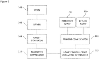
- the apparatus shown comprises a vertical cavity surface emitting laser (VCSEL) 101 which is configured to generate light intensity based on a supplied current (and voltage) provided by a driver 103.
- VCSEL vertical cavity surface emitting laser
- the driver 103 furthermore is configured to generate a current of which a part of is controlled based on an input from an offset generator 105.
- the apparatus may be configured such that the output of the VCSEL has an internal (or parasitic path) to a reference array 107.
- light generated by the VCSEL is internally coupled to a first single photon avalanche diode (SPAD) array which may provide a reference value of the light intensity generated by the VCSEL.
- SPAD single photon avalanche diode
- the apparatus may furthermore be configured such that the output of the VCSEL has an external or free space path to a return array 109.
- light generated by the VCSEL may be externally coupled to at least one further single photon avalanche diode (SPAD) array which may provide a reference value of the light intensity generated by the VCSEL and which has been reflected from an external object.
- SPAD single photon avalanche diode
- the reference array 107 is used to produce a reference signal however in some embodiments the return array 109 can be used as well as the reference array 107 or instead of the reference array 109. For example in some embodiments the apparatus may not have a reference array 107 and use the return array instead to generate the reference signal.
- the apparatus may further comprise an ambient compensator 111.
- the ambient compensator 111 is configured to receive the reference signal from the reference array 107 and/or return array 109 and determine a suitable ambient compensated signal representing the light intensity of the VCSEL. In other words the ambient compensator 111 may be configured to remove any ambient components from the reference signal.
- the apparatus may further comprise a lowest bin selector/parameter determiner 113.
- the lowest bin selector/parameter determiner 113 may be configured to receive the ambient compensated reference signal from the ambient compensator and select a suitable parameter to be output.
- the suitable parameter is a lowest bin value.
- the apparatus may furthermore comprise a parameter comparator 115.
- the parameter comparator may be configured to receive the parameter (such as the lowest bin value) and compare the parameter against a parameter value (for example a defined bin value). The output of the comparison may be passed to the offset generator 105 and/or be used to control the output of the offset generator.
- the offset generator 105 is configured to generate an offset value to be supplied to the driver and the feedback loop described herein used to monitor and track the offset voltage to maintain the offset so that the VCSEL is 'on' the threshold value and therefore able to produce light intensity variations which vary in a non-distorted way but without generating a significant dc or offset level.
- a sine waveform and offset value is generated by the offset generator and which via the driver causes the VCSEL to generate a time varying light intensity.
- the reference array may capture a histogram of the light intensity associated with the time varying sine wave driver output.
- step 301 The operation of capturing the histogram of the sine driver output from the reference array is shown in Figure 3 by step 301.
- the ambient compensator can then subtract ambient (or dark count rate) counts using a separate ambient bin, or by using a time window to establish the ambient level.
- step 303 The operation of generating the ambient compensated value is shown in Figure 3 by step 303.
- the lowest bin selector can then determine and select the lowest bin value. In other words it can select and output the minimum detected intensity value associated with the minimum value of the sine wave and thus reflects the offset value.
- step 305 The operation of determining the lowest bin value is shown in Figure 3 by step 305.
- the parameter comparator than can compare the lowest bin value against a desired level value.
- the desired level value may be a zero value.
- the comparator may control the offset generator to increase the threshold value and thus move the VCSEL away from the threshold on level.
- the offset generator may be configured to reduce the offset current.
- step 307 The operation of comparing the lowest bin value with the zero value and controlling the offset value based on the comparison is shown in Figure 3 by step 307. In some embodiments the operation may then repeat the steps in order to maintain the monitoring of the offset current value.
- any suitable tracking method may be employed to monitor the output of the VCSEL and maintain the operation of the VCSEL within a closely defined range.
- more than one threshold value may be employed to track and control the output and/or a hysteresis range defined between two values to prevent continuous changes in the offset value.
- Figure 4 shows a similar method to Figure 3 but with respect to the pulse generation mode of operation.
- a pre-bias offset value is used.
- the pre-bias offset value is generated by the offset generator and which via the driver may cause the VCSEL to generate a visible output.
- the reference array may capture a histogram of the light intensity associated with the pre-bias driver output.
- step 401 The operation of capturing the histogram of the pre-bias driver output from the reference array is shown in Figure 4 by step 401.
- the ambient compensator can then subtract ambient (or dark count rate) counts using a separate ambient bin, or by using a time window to establish the ambient level.
- the parameter determiner can then determine and select a value for comparison.
- the value for comparison which may be selected may be the minimum bin value as we are attempting to control the pre-bias value to be just below the threshold value. However in some embodiments the minimum bin value or some average bin value may be used.
- the parameter comparator than can compare the lowest bin value against at least one desired level value.
- the desired level value may be a value close to but not equal to zero.
- the comparator may control the offset generator to decrease the pre-bias value and thus control the VCSEL to operate at about the threshold on level.
- the offset generator may be configured to increase the pre-bias level.
- step 407 The operation of comparing the lowest bin value with the threshold value and controlling the offset value based on the comparison is shown in Figure 4 by step 407. In some embodiments the operation may then repeat the steps in order to maintain the monitoring of the pre-bias offset current value.
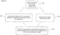
- Figure 5 furthermore shows a similar method to the operations shown in Figure 3 where the time varying waveform is a sine wave with an offset component, but where the determined or selected parameter is based on a Fourier analysis of the (ambient compensated) reference array signal.
- the use of Fourier analysis enables the determination of harmonic strength away from the fundamental.
- the offset may be controlled such that it is increased where the distortion level is too high.
- a sine waveform and offset value is generated by the offset generator and which via the driver causes the VCSEL to generate a time varying light intensity.
- the reference array may capture a histogram of the light intensity associated with the time varying sine wave driver output.
- step 501 The operation of capturing the histogram of the sine driver output from the reference array is shown in Figure 5 by step 501.
- the ambient compensator can then subtract ambient (or dark count rate) counts using a separate ambient bin, or by using a time window to establish the ambient level.
- the parameter selector may than apply a Fourier transform to the ambient compensated values and furthermore determine, a fundamental frequency strength, harmonic frequency strength (and furthermore in some embodiments dc or zero frequency strength). A ratio of the harmonic to fundamental strength may then be generated to the comparator. In some embodiments a ratio of the dc to fundamental strength may also be generated and passed to the comparator.
- the parameter comparator than can compare the ratio(s) against desired level values and the results of the comparison used to control the offset value. For example when the ratio of harmonic to fundamental frequency increases it represents a situation where the sine wave is being distorted as the VCSEL is operating with an offset which is too low to allow non-distorted responses and thus the offset may be increased. Similarly when the ratio of the dc to fundamental frequency strength increases it represents a situation where the offset component is too high and thus the offset may be decreased.
- step 507 The operation of comparing the ratio(s) with the comparison value(s) and controlling the offset value based on the comparison is shown in Figure 5 by step 507. In some embodiments the operation may then repeat the steps in order to maintain the monitoring of the offset current value.
- Some embodiments may use other sensors, instead of SPADs. These sensors may be integrating photo-sensitive elements capable of receiving light intensity, time of arrival, frequency or phase or amplitude/intensity modulation, wavelength (colour) or other information.
Landscapes
- Physics & Mathematics (AREA)
- Engineering & Computer Science (AREA)
- General Physics & Mathematics (AREA)
- Electromagnetism (AREA)
- Computer Networks & Wireless Communication (AREA)
- Radar, Positioning & Navigation (AREA)
- Remote Sensing (AREA)
- Optics & Photonics (AREA)
- Condensed Matter Physics & Semiconductors (AREA)
- Semiconductor Lasers (AREA)
- Optical Radar Systems And Details Thereof (AREA)
- Circuit Arrangement For Electric Light Sources In General (AREA)
- Lighting Device Outwards From Vehicle And Optical Signal (AREA)
Abstract
Description
- Some embodiments relate to an apparatus and in particular but not exclusively to an apparatus with an array of photosensitive devices.
- Single photon avalanche diode (SPAD) time of flight sensors typically comprise arrays of single photon avalanche diodes and an illumination source in the form of a vertical cavity surface emitting laser (VCSEL). The vertical cavity surface emitting laser is provided with current by a driver circuit which is typically configured to be able to control the current through the laser in order to produce pulse or other waveform outputs.
- Typically the vertical cavity surface emitting laser has a threshold current above which the laser is able to emit light (and similarly below which the laser does not emit anything).
- However this threshold current level is not well defined and may change significantly based on many variables such as temperature and process variations.
- According to a first aspect there is provided an apparatus comprising: an illumination source configured to emit light when driven with a current greater than a threshold current; driver circuitry configured to drive the illumination source with a controllable current, the driver circuit controlled by at least a first input value; at least one illumination detector configured to detect light emitted by the illumination source; and monitor circuitry configured to receive an output from the illumination detector and provide the first input value.
- The monitor circuitry may comprise: an ambient compensator configured to receive the output from the at least one illumination detector and output an ambient compensated value; a parameter determiner configured to determine at least one parameter value to be compared based on the ambient compensated value; a parameter comparator configured to compare the at least one parameter value against at least one threshold value; and an offset generator configured to control the driver circuit to provide the controllable current based on an output from the parameter comparator.
- The parameter determiner may be configured to select an ambient compensated minimum intensity value from the at least one illumination detector.
- The parameter comparator may be configured to compare the ambient compensated minimum intensity value against a first threshold value, and wherein the offset generator may be configured to control the driver circuit to increase the controllable current where the ambient compensated minimum intensity value is close to or below the first threshold value.
- The first threshold value may be zero.
- The parameter comparator may be configured to compare the ambient compensated minimum intensity value against a second threshold value, and wherein the offset generator may be configured to control the driver circuit to decrease the controllable current where the ambient compensated minimum intensity value is close to or above the second threshold value.
- The second threshold value may be above zero.
- The parameter determiner may be configured to determine a ratio of a fundamental frequency signal strength against harmonic frequencies signal strength based on a Fourier analysis of a time sequence of ambient compensated values.
- The parameter comparator may be configured to compare the ratio of a fundamental frequency signal strength against harmonic frequencies signal strength against a first threshold value, and wherein the offset generator may be configured to control the driver circuit to increase the controllable current where the ratio of a fundamental frequency signal strength against harmonic frequencies signal strength is close to or below the first threshold value.
- The parameter determiner may be configured to determine a ratio of a fundamental frequency signal strength against zero or dc frequency signal strength based on a Fourier analysis of a time sequence of ambient compensated values.
- The parameter comparator may be configured to compare the ratio of a fundamental frequency signal strength against zero or dc frequency signal strength against a second threshold value, and wherein the offset generator may be configured to control the driver circuit to decrease the controllable current where the ratio of a fundamental frequency signal strength against zero or dc frequency signal strength is close to or above the second threshold value.
- The monitor circuitry may be configured to provide at least one of: the first input value to pre-bias the illumination source operating in a pulsed mode such that the illumination source is driven with a current substantially at the threshold current before the pulse is initiated; and the first input value so to pre-bias the illumination source operating in a time-varying wave mode such that the illumination source responds substantially linearly for any increase in the controllable current.
- The illumination source may be at least one of: a vertical cavity surface emitting laser (VCSEL); and a light emitting diode.
- The apparatus may be a single photon avalanche diode based range detecting sensor, wherein the illumination detector may comprise at least one of: a single photon avalanche diode return array; and a single photon avalanche diode reference array.
- According to a second aspect there is provided a method comprising: providing an illumination source configured to emit light when driven with a current greater than a threshold current; driving with driver circuitry the illumination source with a controllable current, the driver circuit controlled by at least a first input value; detecting light emitted by the illumination source with at least one illumination detector; and receiving at monitor circuitry the output from illumination detector; and controlling the first input value using the monitor circuitry.
- Controlling the first input value using the monitor circuitry may comprise: generating an ambient compensated value based on the received illumination detector output; determining at least one parameter value based on the ambient compensated value; comparing the at least one parameter value against at least one threshold value; and controlling the driver circuit to provide the controllable current based on the comparing.
- Determining the at least one parameter value may comprise selecting an ambient compensated minimum intensity value.
- Comparing the at least one parameter value against the at least one threshold value may comprise comparing the ambient compensated minimum intensity value against a first threshold value, and controlling the driver circuit to provide the controllable current based on the comparing may comprise controlling the driver circuit to increase the controllable current where the ambient compensated minimum intensity value is close to or below the first threshold value.
- The first threshold value may be zero.
- Comparing the at least one parameter value against the at least one threshold value may comprise comparing the ambient compensated minimum intensity value against a second threshold value, and wherein controlling the driver circuit to provide the controllable current based on the comparing may comprise controlling the driver circuit to decrease the controllable current where the ambient compensated minimum intensity value is close to or above the second threshold value.
- The second threshold value may be above zero.
- Determining at least one parameter value based on the ambient compensated value parameter determiner may comprise determining a ratio of a fundamental frequency signal strength against harmonic frequencies signal strength based on a Fourier analysis of a time sequence of ambient compensated values.
- Comparing the at least one parameter value against the at least one threshold value may comprise comparing the ratio of a fundamental frequency signal strength against harmonic frequencies signal strength against a first threshold value, and wherein the controlling the driver circuit to provide the controllable current based on the comparing may comprise controlling the driver circuit to increase the controllable current where the ratio of a fundamental frequency signal strength against harmonic frequencies signal strength is close to or below the first threshold value.
- Determining at least one parameter value based on the ambient compensated value parameter determiner may comprise determining a ratio of a fundamental frequency signal strength against zero or dc frequency signal strength based on a Fourier analysis of a time sequence of ambient compensated values.
- Comparing the at least one parameter value against the at least one threshold value may comprise comparing the ratio of a fundamental frequency signal strength against zero or dc frequency signal strength against a second threshold value, and wherein the controlling the driver circuit to provide the controllable current based on the comparing may comprise controlling the driver circuit to decrease the controllable current where the ratio of a fundamental frequency signal strength against zero or dc frequency signal strength is close to or above the second threshold value.
- Controlling the driver circuit to provide the controllable current based on the comparing may comprise providing at least one of: the first input value to pre-bias the illumination source operating in a pulsed mode such that the illumination source is driven with a current substantially at the threshold current before the pulse is initiated; and the first input value so to pre-bias the illumination source operating in a time-varying wave mode such that the illumination source responds substantially linearly for any increase in the controllable current.
- The illumination source may be at least one of: a vertical cavity surface emitting laser (VCSEL); and a light emitting diode.
- The method may be a method for operating a single photon avalanche diode based range detecting sensor, wherein detecting light emitted by the illumination source with at least one illumination detector may comprise at least one of: detecting light emitted by the illumination source with a single photon avalanche diode return array; and detecting light emitted by the illumination source with a single photon avalanche diode reference array.
- Some embodiments will now be described by way of example only and with reference to the accompanying Figures in which:
-
Fig. 1 shows a schematic view of example current drive waveforms with varying levels of offset current applied to the waveform; -
Fig. 2 shows a schematic view of an example apparatus for controlling the driving current according to some embodiments; -
Fig. 3 shows a flow diagram showing the operation of the example apparatus according to a first set of embodiments; -
Fig. 4 shows a flow diagram showing the operation of the example apparatus according to a second set of embodiments; and -
Fig. 5 shows a flow diagram showing the operation of the example apparatus according to a third set of embodiments. - The concept as employed herein is to implement and configure a SPAD TOF sensor module and in particular the driver current offset to attempt to set the offset such that it matches the vertical cavity surface emitting laser (VCSEL) threshold current requirements independent on the process parameters or operating parameters of the VCSEL.
- As described previously the VCSEL requires a drive current which is above a threshold level in order to produce an output. In order to achieve this the driver is operated using an offset value.
- This offset value can be typically configured to be the value slightly below the level required to cause the driver to provide a current.
- The SPAD TOF sensor when operating the laser in a pulse mode, typically requires the VCSEL to be able to switch on and off quickly. The driver is configured to operate like a switch and is not designed with much consideration about the shape of the rise or fall of the switch profile.
- Although the switching off of the pulse does not critically depend on the VCSEL threshold (or switch on) current, in order to produce fast switching at higher frequencies the driver can provide an offset such that the VCSEL is either at or very close to the threshold current level. Thus in order to be able to achieve fast switch frequencies the concept as described herein is one in which the VCSEL operations are monitored to determine whether the offset voltage for the drivers is causing the driver to be operated as close as possible to the threshold level value.
- SPAD TOF sensors (and also VCSELs) can also be operated to generate a required waveform other than a pulse. In such circumstances the driver may be configured to modulate the drive current such that the VCSEL generates a light intensity output which has a time varying waveform. An example of a useful time varying waveform is a sine wave. In such examples the driver offset should be designed or configured such that the driver current is at the VCSEL operating threshold value (or minimum operating value) in order that any modulation of the driver circuit produces an effective time varying change in the light intensity. Preferably furthermore the relationship between the time varying light intensity waveform and the driver modulation is linear (or as near as being a linear relationship as possible).
- The threshold value of a vertical cavity surface emitting laser is not well defined and can be affected by many different operational parameters. For example it is known that process variations may cause difference between the threshold values in two devices. Furthermore even for a single device the threshold value may vary significantly based on the operating temperature and the supply voltage as well as other characteristics.
-
Figure 1 for example shows the effect of operating the VCSEL at offset values which are significantly below the threshold value, at the threshold value and above the threshold value. - For example in order to guarantee that the VCSEL produces a fast and linear response the driver could be operated with the offset value that is significantly above the threshold. However by operating the laser significantly above the threshold there is always a DC (or offset) component added to the light intensity. This increases the noise, from Photon Shot Noise contribution, and thus reduces the signal to noise ratio (at the receiver). This effect is shown in
Figure 1 by theright hand graph 153 of light intensity output against time for a sine wave applied to the high offset value. - However if the offset value is too low then the VCSEL produces a distorted or non-linear response. This is shown in
Figure 1 by theleft hand graph 151 of light intensity output against time for a sine wave applied to the low offset value where some of the sine wave signals are clipped. - Where the offset value is about the threshold value then the output represents a linear representation of the input. This is shown in
Figure 1 by thecentre graph 152 of light intensity output against time for a sine wave which shows a light intensity which is neither clipped nor contains significantly more noise. - The concept of this application as described hereafter is apparatus and methods for monitoring the output intensity of a VCSEL (and using for example suitable SPAD ToF sensor apparatus where possible) in order to tune the offset current such that the offset current matches or takes into account the variability of the threshold current required to operate the driver and drive the light emitting device such as the VCSEL.
- With respect to
Figure 2 an example apparatus for implementing the embodiments of the concept is shown. The apparatus may in some embodiments be a SPAD ToF sensor device. - The apparatus shown comprises a vertical cavity surface emitting laser (VCSEL) 101 which is configured to generate light intensity based on a supplied current (and voltage) provided by a
driver 103. - The
driver 103 furthermore is configured to generate a current of which a part of is controlled based on an input from an offsetgenerator 105. - The apparatus may be configured such that the output of the VCSEL has an internal (or parasitic path) to a
reference array 107. In other words light generated by the VCSEL is internally coupled to a first single photon avalanche diode (SPAD) array which may provide a reference value of the light intensity generated by the VCSEL. - The apparatus may furthermore be configured such that the output of the VCSEL has an external or free space path to a
return array 109. In other words light generated by the VCSEL may be externally coupled to at least one further single photon avalanche diode (SPAD) array which may provide a reference value of the light intensity generated by the VCSEL and which has been reflected from an external object. - In the following examples the
reference array 107 is used to produce a reference signal however in some embodiments thereturn array 109 can be used as well as thereference array 107 or instead of thereference array 109. For example in some embodiments the apparatus may not have areference array 107 and use the return array instead to generate the reference signal. - The apparatus may further comprise an
ambient compensator 111. Theambient compensator 111 is configured to receive the reference signal from thereference array 107 and/or returnarray 109 and determine a suitable ambient compensated signal representing the light intensity of the VCSEL. In other words theambient compensator 111 may be configured to remove any ambient components from the reference signal. - The apparatus may further comprise a lowest bin selector/
parameter determiner 113. The lowest bin selector/parameter determiner 113 may be configured to receive the ambient compensated reference signal from the ambient compensator and select a suitable parameter to be output. In some embodiments the suitable parameter is a lowest bin value. - The apparatus may furthermore comprise a
parameter comparator 115. The parameter comparator may be configured to receive the parameter (such as the lowest bin value) and compare the parameter against a parameter value (for example a defined bin value). The output of the comparison may be passed to the offsetgenerator 105 and/or be used to control the output of the offset generator. As described previously the offsetgenerator 105 is configured to generate an offset value to be supplied to the driver and the feedback loop described herein used to monitor and track the offset voltage to maintain the offset so that the VCSEL is 'on' the threshold value and therefore able to produce light intensity variations which vary in a non-distorted way but without generating a significant dc or offset level. - With respect to
Figure 3 the example operation of the apparatus shown inFigure 2 according to a first set of embodiments is described in further detail. In this example a sine waveform and offset value is generated by the offset generator and which via the driver causes the VCSEL to generate a time varying light intensity. The reference array may capture a histogram of the light intensity associated with the time varying sine wave driver output. - The operation of capturing the histogram of the sine driver output from the reference array is shown in
Figure 3 bystep 301. - The ambient compensator can then subtract ambient (or dark count rate) counts using a separate ambient bin, or by using a time window to establish the ambient level.
- The operation of generating the ambient compensated value is shown in
Figure 3 bystep 303. - The lowest bin selector can then determine and select the lowest bin value. In other words it can select and output the minimum detected intensity value associated with the minimum value of the sine wave and thus reflects the offset value.
- The operation of determining the lowest bin value is shown in
Figure 3 bystep 305. - The parameter comparator than can compare the lowest bin value against a desired level value. For example the desired level value may be a zero value. In such embodiments where the lowest bin value gets too close to the zero value the comparator may control the offset generator to increase the threshold value and thus move the VCSEL away from the threshold on level. Similarly where the lowest bin value is too high and or above a predetermined value the offset generator may be configured to reduce the offset current.
- The operation of comparing the lowest bin value with the zero value and controlling the offset value based on the comparison is shown in
Figure 3 bystep 307. In some embodiments the operation may then repeat the steps in order to maintain the monitoring of the offset current value. Although the example shown above (and the examples shown below) describe a simple single threshold value comparison and control mechanism it is understood that any suitable tracking method may be employed to monitor the output of the VCSEL and maintain the operation of the VCSEL within a closely defined range. Thus for example more than one threshold value may be employed to track and control the output and/or a hysteresis range defined between two values to prevent continuous changes in the offset value. -
Figure 4 shows a similar method toFigure 3 but with respect to the pulse generation mode of operation. Thus in the example shown inFigure 4 rather than using a sine wave and offset signal for the driver a pre-bias offset value only is used. The pre-bias offset value is generated by the offset generator and which via the driver may cause the VCSEL to generate a visible output. The reference array may capture a histogram of the light intensity associated with the pre-bias driver output. - The operation of capturing the histogram of the pre-bias driver output from the reference array is shown in
Figure 4 bystep 401. - The ambient compensator can then subtract ambient (or dark count rate) counts using a separate ambient bin, or by using a time window to establish the ambient level.
- The operation of generating the ambient compensated value is shown in
Figure 4 bystep 403. - The parameter determiner can then determine and select a value for comparison. For example the value for comparison which may be selected may be the minimum bin value as we are attempting to control the pre-bias value to be just below the threshold value. However in some embodiments the minimum bin value or some average bin value may be used.
- The operation of determining the lowest bin value is shown in
Figure 4 bystep 405. - The parameter comparator than can compare the lowest bin value against at least one desired level value. For example the desired level value may be a value close to but not equal to zero. In such embodiments where the lowest bin value is greater than the value then the comparator may control the offset generator to decrease the pre-bias value and thus control the VCSEL to operate at about the threshold on level. Similarly where the lowest bin value is lower than the value then the offset generator may be configured to increase the pre-bias level.
- The operation of comparing the lowest bin value with the threshold value and controlling the offset value based on the comparison is shown in
Figure 4 bystep 407. In some embodiments the operation may then repeat the steps in order to maintain the monitoring of the pre-bias offset current value. -
Figure 5 furthermore shows a similar method to the operations shown inFigure 3 where the time varying waveform is a sine wave with an offset component, but where the determined or selected parameter is based on a Fourier analysis of the (ambient compensated) reference array signal. The use of Fourier analysis enables the determination of harmonic strength away from the fundamental. In such an embodiments the offset may be controlled such that it is increased where the distortion level is too high. - In this example a sine waveform and offset value is generated by the offset generator and which via the driver causes the VCSEL to generate a time varying light intensity. The reference array may capture a histogram of the light intensity associated with the time varying sine wave driver output.
- The operation of capturing the histogram of the sine driver output from the reference array is shown in
Figure 5 bystep 501. - The ambient compensator can then subtract ambient (or dark count rate) counts using a separate ambient bin, or by using a time window to establish the ambient level.
- The operation of generating the ambient compensated value is shown in
Figure 5 bystep 503. - The parameter selector may than apply a Fourier transform to the ambient compensated values and furthermore determine, a fundamental frequency strength, harmonic frequency strength (and furthermore in some embodiments dc or zero frequency strength). A ratio of the harmonic to fundamental strength may then be generated to the comparator. In some embodiments a ratio of the dc to fundamental strength may also be generated and passed to the comparator.
- The operation of performing a Fourier analysis and determination and outputting the ratio(s) is shown in
Figure 5 bystep 505. - The parameter comparator than can compare the ratio(s) against desired level values and the results of the comparison used to control the offset value. For example when the ratio of harmonic to fundamental frequency increases it represents a situation where the sine wave is being distorted as the VCSEL is operating with an offset which is too low to allow non-distorted responses and thus the offset may be increased. Similarly when the ratio of the dc to fundamental frequency strength increases it represents a situation where the offset component is too high and thus the offset may be decreased.
- The operation of comparing the ratio(s) with the comparison value(s) and controlling the offset value based on the comparison is shown in
Figure 5 bystep 507. In some embodiments the operation may then repeat the steps in order to maintain the monitoring of the offset current value. - Some embodiments may use other sensors, instead of SPADs. These sensors may be integrating photo-sensitive elements capable of receiving light intensity, time of arrival, frequency or phase or amplitude/intensity modulation, wavelength (colour) or other information.
- It should be appreciated that the above described arrangements may be implemented at least partially by an integrated circuit, a chip set, one or more dies packaged together or in different packages, discrete circuitry or any combination of these options.
- Various embodiments with different variations have been described here above. It should be noted that those skilled in the art may combine various elements of these various embodiments and variations.
- Such alterations, modifications, and improvements are intended to be part of this disclosure, and are intended to be within the scope of the present invention. Accordingly, the foregoing description is by way of example only and is not intended to be limiting. The present invention is limited only as defined in the following claims and the equivalents thereto.
Claims (15)
- An apparatus comprising:an illumination source configured to emit light when driven with a current greater than a threshold current;driver circuitry configured to drive the illumination source with a controllable current, the driver circuit controlled by at least a first input value;at least one illumination detector configured to detect light emitted by the illumination source; andmonitor circuitry configured to receive an output from the illumination detector and provide the first input value.
- The apparatus as claimed in claim 1, wherein the monitor circuitry comprises:an ambient compensator configured to receive the output from the at least one illumination detector and output an ambient compensated value;a parameter determiner configured to determine at least one parameter value to be compared based on the ambient compensated value;a parameter comparator configured to compare the at least one parameter value against at least one threshold value; andan offset generator configured to control the driver circuit to provide the controllable current based on an output from the parameter comparator.
- The apparatus as claimed in claim 2, wherein the parameter determiner is configured to select an ambient compensated minimum intensity value from the at least one illumination detector.
- The as claimed in claim 3, wherein the parameter comparator is configured to compare the ambient compensated minimum intensity value against a first threshold value, and wherein the offset generator is configured to control the driver circuit to increase the controllable current where the ambient compensated minimum intensity value is close to or below the first threshold value.
- The apparatus as claimed in claim 4, wherein the first threshold value is zero.
- apparatus as claimed in any of claims 3 to 5, wherein the parameter comparator is configured to compare the ambient compensated minimum intensity value against a second threshold value, and wherein the offset generator is configured to control the driver circuit to decrease the controllable current where the ambient compensated minimum intensity value is close to or above the second threshold value.
- The apparatus as claimed in claim 6, wherein the second threshold value is above zero.
- The apparatus as claimed in claim 2, wherein the parameter determiner is configured to determine a ratio of a fundamental frequency signal strength against harmonic frequencies signal strength based on a Fourier analysis of a time sequence of ambient compensated values.
- The apparatus as claimed in claim 8, wherein the parameter comparator is configured to compare the ratio of a fundamental frequency signal strength against harmonic frequencies signal strength against a first threshold value, and wherein the offset generator is configured to control the driver circuit to increase the controllable current where the ratio of a fundamental frequency signal strength against harmonic frequencies signal strength is close to or below the first threshold value.
- The apparatus as claimed in any of claims 2, 8 or 9, wherein the parameter determiner is configured to determine a ratio of a fundamental frequency signal strength against zero or dc frequency signal strength based on a Fourier analysis of a time sequence of ambient compensated values.
- The apparatus as claimed in claim 10, wherein the parameter comparator is configured to compare the ratio of a fundamental frequency signal strength against zero or dc frequency signal strength against a second threshold value, and wherein the offset generator is configured to control the driver circuit to decrease the controllable current where the ratio of a fundamental frequency signal strength against zero or dc frequency signal strength is close to or above the second threshold value.
- The apparatus as claimed in any of claims 1 to 11, wherein the monitor circuitry is configured to provide at least one of:the first input value to pre-bias the illumination source operating in a pulsed mode such that the illumination source is driven with a current substantially at the threshold current before the pulse is initiated; andthe first input value so to pre-bias the illumination source operating in a time-varying wave mode such that the illumination source responds substantially linearly for any increase in the controllable current.
- The apparatus as claimed in any of claims 1 to 12, wherein the illumination source is at least one of:a vertical cavity surface emitting laser (VCSEL); anda light emitting diode.
- The apparatus as claimed in any of claims 1 to 13, is a single photon avalanche diode based range detecting sensor, wherein the illumination detector comprises at least one of:a single photon avalanche diode return array; anda single photon avalanche diode reference array.
- A method comprising:providing an illumination source configured to emit light when driven with a current greater than a threshold current;driving with driver circuitry the illumination source with a controllable current, the driver circuit controlled by at least a first input value;detecting light emitted by the illumination source with at least one illumination detector; andreceiving at monitor circuitry the output from illumination detector; andcontrolling the first input value using the monitor circuitry.
Priority Applications (5)
| Application Number | Priority Date | Filing Date | Title |
|---|---|---|---|
| EP16193533.3A EP3309581B1 (en) | 2016-10-12 | 2016-10-12 | Apparatus for controlling driver current for illumination source |
| US15/610,013 US10264653B2 (en) | 2016-10-12 | 2017-05-31 | Apparatus for controlling driver current for illumination source |
| CN201710491745.6A CN107946903B (en) | 2016-10-12 | 2017-06-23 | Apparatus for controlling the drive current of a lighting source |
| CN202011415242.9A CN112543535B (en) | 2016-10-12 | 2017-06-23 | Apparatus for controlling the drive current of an illumination source |
| CN201720747160.1U CN207134606U (en) | 2016-10-12 | 2017-06-23 | Apparatus for controlling the drive current of an illumination source |
Applications Claiming Priority (1)
| Application Number | Priority Date | Filing Date | Title |
|---|---|---|---|
| EP16193533.3A EP3309581B1 (en) | 2016-10-12 | 2016-10-12 | Apparatus for controlling driver current for illumination source |
Publications (2)
| Publication Number | Publication Date |
|---|---|
| EP3309581A1 true EP3309581A1 (en) | 2018-04-18 |
| EP3309581B1 EP3309581B1 (en) | 2025-11-26 |
Family
ID=57211274
Family Applications (1)
| Application Number | Title | Priority Date | Filing Date |
|---|---|---|---|
| EP16193533.3A Active EP3309581B1 (en) | 2016-10-12 | 2016-10-12 | Apparatus for controlling driver current for illumination source |
Country Status (3)
| Country | Link |
|---|---|
| US (1) | US10264653B2 (en) |
| EP (1) | EP3309581B1 (en) |
| CN (3) | CN112543535B (en) |
Families Citing this family (36)
| Publication number | Priority date | Publication date | Assignee | Title |
|---|---|---|---|---|
| US10158038B1 (en) | 2018-05-17 | 2018-12-18 | Hi Llc | Fast-gated photodetector architectures comprising dual voltage sources with a switch configuration |
| US10340408B1 (en) | 2018-05-17 | 2019-07-02 | Hi Llc | Non-invasive wearable brain interface systems including a headgear and a plurality of self-contained photodetector units configured to removably attach to the headgear |
| US10515993B2 (en) | 2018-05-17 | 2019-12-24 | Hi Llc | Stacked photodetector assemblies |
| US10420498B1 (en) | 2018-06-20 | 2019-09-24 | Hi Llc | Spatial and temporal-based diffusive correlation spectroscopy systems and methods |
| US11213206B2 (en) | 2018-07-17 | 2022-01-04 | Hi Llc | Non-invasive measurement systems with single-photon counting camera |
| WO2020087376A1 (en) * | 2018-10-31 | 2020-05-07 | 深圳市大疆创新科技有限公司 | Light detection method, light detection device, and mobile platform |
| WO2020131148A1 (en) | 2018-12-21 | 2020-06-25 | Hi Llc | Biofeedback for awareness and modulation of mental state using a non-invasive brain interface system and method |
| AU2020268718B2 (en) | 2019-05-06 | 2025-04-03 | Hi Llc | Photodetector architectures for time-correlated single photon counting |
| WO2020236371A1 (en) | 2019-05-21 | 2020-11-26 | Hi Llc | Photodetector architectures for efficient fast-gating |
| US11579290B2 (en) | 2019-06-05 | 2023-02-14 | Stmicroelectronics (Research & Development) Limited | LIDAR system utilizing multiple networked LIDAR integrated circuits |
| US11728621B2 (en) | 2019-06-05 | 2023-08-15 | Stmicroelectronics (Research & Development) Limited | Voltage controlled steered VCSEL driver |
| CA3137921A1 (en) | 2019-06-06 | 2020-12-10 | Hi Llc | Photodetector systems with low-power time-to-digital converter architectures |
| US12029558B2 (en) | 2020-02-21 | 2024-07-09 | Hi Llc | Time domain-based optical measurement systems and methods configured to measure absolute properties of tissue |
| US11630310B2 (en) | 2020-02-21 | 2023-04-18 | Hi Llc | Wearable devices and wearable assemblies with adjustable positioning for use in an optical measurement system |
| US12144653B2 (en) | 2020-02-21 | 2024-11-19 | Hi Llc | Systems, circuits, and methods for reducing common-mode noise in biopotential recordings |
| US11883181B2 (en) | 2020-02-21 | 2024-01-30 | Hi Llc | Multimodal wearable measurement systems and methods |
| WO2021167890A1 (en) | 2020-02-21 | 2021-08-26 | Hi Llc | Wearable module assemblies for an optical measurement system |
| WO2021167876A1 (en) | 2020-02-21 | 2021-08-26 | Hi Llc | Methods and systems for initiating and conducting a customized computer-enabled brain research study |
| US11950879B2 (en) | 2020-02-21 | 2024-04-09 | Hi Llc | Estimation of source-detector separation in an optical measurement system |
| US11771362B2 (en) | 2020-02-21 | 2023-10-03 | Hi Llc | Integrated detector assemblies for a wearable module of an optical measurement system |
| US11969259B2 (en) | 2020-02-21 | 2024-04-30 | Hi Llc | Detector assemblies for a wearable module of an optical measurement system and including spring-loaded light-receiving members |
| US11877825B2 (en) | 2020-03-20 | 2024-01-23 | Hi Llc | Device enumeration in an optical measurement system |
| US11903676B2 (en) | 2020-03-20 | 2024-02-20 | Hi Llc | Photodetector calibration of an optical measurement system |
| WO2021188488A1 (en) | 2020-03-20 | 2021-09-23 | Hi Llc | Bias voltage generation in an optical measurement system |
| US11187575B2 (en) | 2020-03-20 | 2021-11-30 | Hi Llc | High density optical measurement systems with minimal number of light sources |
| US12059262B2 (en) | 2020-03-20 | 2024-08-13 | Hi Llc | Maintaining consistent photodetector sensitivity in an optical measurement system |
| WO2021188487A1 (en) | 2020-03-20 | 2021-09-23 | Hi Llc | Temporal resolution control for temporal point spread function generation in an optical measurement system |
| US11645483B2 (en) | 2020-03-20 | 2023-05-09 | Hi Llc | Phase lock loop circuit based adjustment of a measurement time window in an optical measurement system |
| US11864867B2 (en) | 2020-03-20 | 2024-01-09 | Hi Llc | Control circuit for a light source in an optical measurement system by applying voltage with a first polarity to start an emission of a light pulse and applying voltage with a second polarity to stop the emission of the light pulse |
| US12138068B2 (en) | 2020-03-20 | 2024-11-12 | Hi Llc | Techniques for characterizing a nonlinearity of a time-to-digital converter in an optical measurement system |
| US11819311B2 (en) | 2020-03-20 | 2023-11-21 | Hi Llc | Maintaining consistent photodetector sensitivity in an optical measurement system |
| US11245404B2 (en) | 2020-03-20 | 2022-02-08 | Hi Llc | Phase lock loop circuit based signal generation in an optical measurement system |
| US11857348B2 (en) | 2020-03-20 | 2024-01-02 | Hi Llc | Techniques for determining a timing uncertainty of a component of an optical measurement system |
| US12059270B2 (en) | 2020-04-24 | 2024-08-13 | Hi Llc | Systems and methods for noise removal in an optical measurement system |
| CN112998627B (en) * | 2021-03-03 | 2022-07-01 | 重庆金山医疗技术研究院有限公司 | Endoscope light flux automatic detection compensation method and endoscope system |
| US11881129B2 (en) * | 2021-04-30 | 2024-01-23 | Microsoft Technology Licensing, Llc | Systems and methods for adding persistence to single photon avalanche diode imagery |
Citations (3)
| Publication number | Priority date | Publication date | Assignee | Title |
|---|---|---|---|---|
| US20020029103A1 (en) * | 1995-06-07 | 2002-03-07 | Breed David S. | Vehicle rear seat monitor |
| EP1511136A1 (en) * | 2003-09-01 | 2005-03-02 | Robert Bosch Gmbh | Electromagnetic transmitter system |
| US20120051379A1 (en) * | 2010-08-27 | 2012-03-01 | Chih-Yang Wang | Automatic power control (apc) loop for adjusting the bias current of a laser diode |
Family Cites Families (29)
| Publication number | Priority date | Publication date | Assignee | Title |
|---|---|---|---|---|
| US4344173A (en) * | 1978-09-25 | 1982-08-10 | Northern Telecom Limited | Stabilization circuit for a digitally operated laser |
| US4621376A (en) * | 1983-04-28 | 1986-11-04 | Kabushiki Kaisha Toshiba | Driving apparatus for stabilizing burst light output |
| JPS60110183A (en) * | 1983-11-18 | 1985-06-15 | Nec Corp | Photooutput stabilizing circuit |
| DE3684079D1 (en) * | 1985-09-30 | 1992-04-09 | Toshiba Kawasaki Kk | DEVICE FOR STABILIZING THE OPTICAL OUTPUT PERFORMANCE OF A SEMICONDUCTOR LASER. |
| EP0497431B1 (en) * | 1987-04-13 | 1995-06-28 | Sharp Kabushiki Kaisha | An apparatus for driving a semiconductor laser device |
| JP2613670B2 (en) * | 1990-09-28 | 1997-05-28 | シャープ株式会社 | Drive circuit for semiconductor laser |
| US5402433A (en) * | 1994-01-05 | 1995-03-28 | Alcatel Network Systems, Inc. | Apparatus and method for laser bias and modulation control |
| GB9421329D0 (en) * | 1994-10-22 | 1994-12-07 | Bt & D Technologies Ltd | Laser bias control system |
| US5754577A (en) * | 1996-07-23 | 1998-05-19 | Broadband Communications Products, Inc. | Compensation for variations in temperature and aging of laser diode by use of small signal, square-law portion of transfer function of diode detection circuit |
| US6078601A (en) * | 1997-03-07 | 2000-06-20 | Smith; David F. | Method for controlling the operation of a laser |
| JP4205916B2 (en) * | 2002-09-03 | 2009-01-07 | パナソニック株式会社 | Extinction ratio compensation laser drive circuit and optical communication device |
| US7256470B2 (en) * | 2005-03-16 | 2007-08-14 | Udt Sensors, Inc. | Photodiode with controlled current leakage |
| JP2006013252A (en) * | 2004-06-28 | 2006-01-12 | Hitachi Cable Ltd | Laser diode control method, control circuit, and optical transmitter |
| US7608806B2 (en) * | 2004-11-19 | 2009-10-27 | Mindspeed Technologies, Inc. | Multiple parameter laser power control with automatic compensation |
| JP4788547B2 (en) * | 2006-09-26 | 2011-10-05 | 住友電気工業株式会社 | Laser diode drive circuit |
| KR100884484B1 (en) * | 2007-05-15 | 2009-02-17 | 호서대학교 산학협력단 | Optical transmitter with automatic temperature compensation |
| WO2009019655A2 (en) * | 2007-08-07 | 2009-02-12 | Koninklijke Philips Electronics N.V. | Method and apparatus for discriminating modulated light in a mixed light system |
| JP5542303B2 (en) * | 2007-12-28 | 2014-07-09 | ソニー株式会社 | Light source system and display device |
| US8729870B2 (en) * | 2008-08-15 | 2014-05-20 | Analog Modules, Inc. | Biphase laser diode driver and method |
| US8222591B2 (en) * | 2009-07-07 | 2012-07-17 | Intersil Americas Inc. | Proximity sensors with improved ambient light rejection |
| US8766161B2 (en) * | 2009-12-02 | 2014-07-01 | Nucript LLC | System for controling and calibrating single photon detection devices |
| WO2011132759A1 (en) * | 2010-04-21 | 2011-10-27 | 日本電気株式会社 | Optical receiver, optical reception device, and correction method for optical reception strength |
| CN102013630A (en) * | 2010-10-09 | 2011-04-13 | 维林光电(苏州)有限公司 | Semiconductor laser module, method for stabilizing and denoising semiconductor laser, and solid laser |
| EP2648482A1 (en) * | 2012-04-05 | 2013-10-09 | Koninklijke Philips N.V. | LED lighting system |
| KR20150054530A (en) * | 2013-11-12 | 2015-05-20 | 한국전자통신연구원 | Laser driver for ABC and AMC compensates temperature effects of laser |
| CN104078841B (en) * | 2014-07-08 | 2018-02-09 | 成都新易盛通信技术股份有限公司 | A kind of optical module laser digital Open loop temperature compensation system |
| EP3674214A1 (en) * | 2014-10-17 | 2020-07-01 | Sony Corporation | Control device, control method, and flight vehicle device |
| CN104579458A (en) * | 2014-12-30 | 2015-04-29 | 上海贝岭股份有限公司 | Light power compensation method and circuit |
| EP4117202B1 (en) * | 2021-07-09 | 2026-01-07 | Mitsubishi Electric R & D Centre Europe B.V. | Coherent optical receiver |
-
2016
- 2016-10-12 EP EP16193533.3A patent/EP3309581B1/en active Active
-
2017
- 2017-05-31 US US15/610,013 patent/US10264653B2/en active Active
- 2017-06-23 CN CN202011415242.9A patent/CN112543535B/en active Active
- 2017-06-23 CN CN201720747160.1U patent/CN207134606U/en not_active Withdrawn - After Issue
- 2017-06-23 CN CN201710491745.6A patent/CN107946903B/en active Active
Patent Citations (3)
| Publication number | Priority date | Publication date | Assignee | Title |
|---|---|---|---|---|
| US20020029103A1 (en) * | 1995-06-07 | 2002-03-07 | Breed David S. | Vehicle rear seat monitor |
| EP1511136A1 (en) * | 2003-09-01 | 2005-03-02 | Robert Bosch Gmbh | Electromagnetic transmitter system |
| US20120051379A1 (en) * | 2010-08-27 | 2012-03-01 | Chih-Yang Wang | Automatic power control (apc) loop for adjusting the bias current of a laser diode |
Also Published As
| Publication number | Publication date |
|---|---|
| CN112543535B (en) | 2023-07-28 |
| US20180103528A1 (en) | 2018-04-12 |
| US10264653B2 (en) | 2019-04-16 |
| CN112543535A (en) | 2021-03-23 |
| CN207134606U (en) | 2018-03-23 |
| EP3309581B1 (en) | 2025-11-26 |
| CN107946903A (en) | 2018-04-20 |
| CN107946903B (en) | 2020-12-11 |
Similar Documents
| Publication | Publication Date | Title |
|---|---|---|
| US10264653B2 (en) | Apparatus for controlling driver current for illumination source | |
| KR101770872B1 (en) | TOF camera for vehicle and method for driving thereof | |
| US11397249B2 (en) | Light detection device and electronic apparatus comprising a reverse bias voltage adjustment in accordance with a pulse number output by a first SPAD array | |
| US10132926B2 (en) | Range finder, mobile object and range-finding method | |
| JP6413960B2 (en) | Distance measuring device | |
| US20120293783A1 (en) | Light source drive device, optical scanning device and image forming apparatus | |
| US10454246B2 (en) | Optical pulse emitter | |
| US11754684B2 (en) | Optical light emitter device and method | |
| US6781677B1 (en) | Laser range finding apparatus | |
| JP2022091847A (en) | Controls, detectors, methods for controlling avalanche diodes, programs and storage media | |
| US20240019559A1 (en) | Lidar system and its control method | |
| US11061138B2 (en) | Distance measuring device and method of measuring distance by using the same | |
| US10317530B2 (en) | Laser range finding apparatus | |
| KR20210094637A (en) | Light source operating device for optical TOF measurement | |
| US11733358B2 (en) | Electronic circuit and time-of-flight sensor comprising such an electronic circuit | |
| JP2646898B2 (en) | Laser distance measuring device | |
| KR102343294B1 (en) | Lidar System and its Control Method | |
| CN112332213A (en) | Laser driving circuit with human eye protection function and method thereof | |
| KR20190143332A (en) | Beam projector module for preventing malfunction of eye-safety function, and control method thereof | |
| KR102695035B1 (en) | Laser diode driver | |
| CN101517520A (en) | Laser controller | |
| JP7285960B2 (en) | Cumulative short-pulse radiation from a long-irradiation pulsed lidar device | |
| JP2020106350A (en) | Light projection/receiving device, light projection/receiving method, program, and recording medium | |
| US20020038846A1 (en) | Optical detector with regulated emission | |
| KR20210039206A (en) | Laser driver apparatus and operating method thereof with auto control de-emphasis |
Legal Events
| Date | Code | Title | Description |
|---|---|---|---|
| PUAI | Public reference made under article 153(3) epc to a published international application that has entered the european phase |
Free format text: ORIGINAL CODE: 0009012 |
|
| STAA | Information on the status of an ep patent application or granted ep patent |
Free format text: STATUS: THE APPLICATION HAS BEEN PUBLISHED |
|
| AK | Designated contracting states |
Kind code of ref document: A1 Designated state(s): AL AT BE BG CH CY CZ DE DK EE ES FI FR GB GR HR HU IE IS IT LI LT LU LV MC MK MT NL NO PL PT RO RS SE SI SK SM TR |
|
| AX | Request for extension of the european patent |
Extension state: BA ME |
|
| STAA | Information on the status of an ep patent application or granted ep patent |
Free format text: STATUS: REQUEST FOR EXAMINATION WAS MADE |
|
| 17P | Request for examination filed |
Effective date: 20181017 |
|
| RBV | Designated contracting states (corrected) |
Designated state(s): AL AT BE BG CH CY CZ DE DK EE ES FI FR GB GR HR HU IE IS IT LI LT LU LV MC MK MT NL NO PL PT RO RS SE SI SK SM TR |
|
| STAA | Information on the status of an ep patent application or granted ep patent |
Free format text: STATUS: EXAMINATION IS IN PROGRESS |
|
| 17Q | First examination report despatched |
Effective date: 20190513 |
|
| GRAP | Despatch of communication of intention to grant a patent |
Free format text: ORIGINAL CODE: EPIDOSNIGR1 |
|
| STAA | Information on the status of an ep patent application or granted ep patent |
Free format text: STATUS: GRANT OF PATENT IS INTENDED |
|
| INTG | Intention to grant announced |
Effective date: 20250124 |
|
| GRAJ | Information related to disapproval of communication of intention to grant by the applicant or resumption of examination proceedings by the epo deleted |
Free format text: ORIGINAL CODE: EPIDOSDIGR1 |
|
| STAA | Information on the status of an ep patent application or granted ep patent |
Free format text: STATUS: EXAMINATION IS IN PROGRESS |
|
| GRAP | Despatch of communication of intention to grant a patent |
Free format text: ORIGINAL CODE: EPIDOSNIGR1 |
|
| STAA | Information on the status of an ep patent application or granted ep patent |
Free format text: STATUS: GRANT OF PATENT IS INTENDED |
|
| INTC | Intention to grant announced (deleted) | ||
| INTG | Intention to grant announced |
Effective date: 20250520 |
|
| GRAS | Grant fee paid |
Free format text: ORIGINAL CODE: EPIDOSNIGR3 |
|
| GRAA | (expected) grant |
Free format text: ORIGINAL CODE: 0009210 |
|
| STAA | Information on the status of an ep patent application or granted ep patent |
Free format text: STATUS: THE PATENT HAS BEEN GRANTED |
|
| AK | Designated contracting states |
Kind code of ref document: B1 Designated state(s): AL AT BE BG CH CY CZ DE DK EE ES FI FR GB GR HR HU IE IS IT LI LT LU LV MC MK MT NL NO PL PT RO RS SE SI SK SM TR |
|
| REG | Reference to a national code |
Ref country code: CH Ref legal event code: F10 Free format text: ST27 STATUS EVENT CODE: U-0-0-F10-F00 (AS PROVIDED BY THE NATIONAL OFFICE) Effective date: 20251126 Ref country code: GB Ref legal event code: FG4D |
|
| REG | Reference to a national code |
Ref country code: IE Ref legal event code: FG4D |
|
| REG | Reference to a national code |
Ref country code: DE Ref legal event code: R096 Ref document number: 602016094178 Country of ref document: DE |
|
| REG | Reference to a national code |
Ref country code: NL Ref legal event code: MP Effective date: 20251126 |
|
| PG25 | Lapsed in a contracting state [announced via postgrant information from national office to epo] |
Ref country code: ES Free format text: LAPSE BECAUSE OF FAILURE TO SUBMIT A TRANSLATION OF THE DESCRIPTION OR TO PAY THE FEE WITHIN THE PRESCRIBED TIME-LIMIT Effective date: 20251126 |
|
| REG | Reference to a national code |
Ref country code: LT Ref legal event code: MG9D |
|
| PG25 | Lapsed in a contracting state [announced via postgrant information from national office to epo] |
Ref country code: NO Free format text: LAPSE BECAUSE OF FAILURE TO SUBMIT A TRANSLATION OF THE DESCRIPTION OR TO PAY THE FEE WITHIN THE PRESCRIBED TIME-LIMIT Effective date: 20260226 |
|
| PG25 | Lapsed in a contracting state [announced via postgrant information from national office to epo] |
Ref country code: FI Free format text: LAPSE BECAUSE OF FAILURE TO SUBMIT A TRANSLATION OF THE DESCRIPTION OR TO PAY THE FEE WITHIN THE PRESCRIBED TIME-LIMIT Effective date: 20251126 Ref country code: AT Free format text: LAPSE BECAUSE OF FAILURE TO SUBMIT A TRANSLATION OF THE DESCRIPTION OR TO PAY THE FEE WITHIN THE PRESCRIBED TIME-LIMIT Effective date: 20251126 Ref country code: HR Free format text: LAPSE BECAUSE OF FAILURE TO SUBMIT A TRANSLATION OF THE DESCRIPTION OR TO PAY THE FEE WITHIN THE PRESCRIBED TIME-LIMIT Effective date: 20251126 |
|
| REG | Reference to a national code |
Ref country code: AT Ref legal event code: MK05 Ref document number: 1861571 Country of ref document: AT Kind code of ref document: T Effective date: 20251126 |
|
| PG25 | Lapsed in a contracting state [announced via postgrant information from national office to epo] |
Ref country code: NL Free format text: LAPSE BECAUSE OF FAILURE TO SUBMIT A TRANSLATION OF THE DESCRIPTION OR TO PAY THE FEE WITHIN THE PRESCRIBED TIME-LIMIT Effective date: 20251126 |
|
| PG25 | Lapsed in a contracting state [announced via postgrant information from national office to epo] |
Ref country code: RS Free format text: LAPSE BECAUSE OF FAILURE TO SUBMIT A TRANSLATION OF THE DESCRIPTION OR TO PAY THE FEE WITHIN THE PRESCRIBED TIME-LIMIT Effective date: 20260226 |
|
| PG25 | Lapsed in a contracting state [announced via postgrant information from national office to epo] |
Ref country code: IS Free format text: LAPSE BECAUSE OF FAILURE TO SUBMIT A TRANSLATION OF THE DESCRIPTION OR TO PAY THE FEE WITHIN THE PRESCRIBED TIME-LIMIT Effective date: 20260326 |
|
| PG25 | Lapsed in a contracting state [announced via postgrant information from national office to epo] |
Ref country code: PT Free format text: LAPSE BECAUSE OF FAILURE TO SUBMIT A TRANSLATION OF THE DESCRIPTION OR TO PAY THE FEE WITHIN THE PRESCRIBED TIME-LIMIT Effective date: 20260326 |
|
| PG25 | Lapsed in a contracting state [announced via postgrant information from national office to epo] |
Ref country code: PL Free format text: LAPSE BECAUSE OF FAILURE TO SUBMIT A TRANSLATION OF THE DESCRIPTION OR TO PAY THE FEE WITHIN THE PRESCRIBED TIME-LIMIT Effective date: 20251126 |
|
| PG25 | Lapsed in a contracting state [announced via postgrant information from national office to epo] |
Ref country code: LV Free format text: LAPSE BECAUSE OF FAILURE TO SUBMIT A TRANSLATION OF THE DESCRIPTION OR TO PAY THE FEE WITHIN THE PRESCRIBED TIME-LIMIT Effective date: 20251126 |
|
| PG25 | Lapsed in a contracting state [announced via postgrant information from national office to epo] |
Ref country code: BG Free format text: LAPSE BECAUSE OF FAILURE TO SUBMIT A TRANSLATION OF THE DESCRIPTION OR TO PAY THE FEE WITHIN THE PRESCRIBED TIME-LIMIT Effective date: 20251126 |