EP3308196B1 - Schaltungsanordnung zur signalerfassung einer vorrichtung zur messung der strahlen geladener teilchen in der externen radiotherapie - Google Patents
Schaltungsanordnung zur signalerfassung einer vorrichtung zur messung der strahlen geladener teilchen in der externen radiotherapie Download PDFInfo
- Publication number
- EP3308196B1 EP3308196B1 EP16744521.2A EP16744521A EP3308196B1 EP 3308196 B1 EP3308196 B1 EP 3308196B1 EP 16744521 A EP16744521 A EP 16744521A EP 3308196 B1 EP3308196 B1 EP 3308196B1
- Authority
- EP
- European Patent Office
- Prior art keywords
- channel
- circuit arrangement
- branches
- outputs
- sensor
- Prior art date
- Legal status (The legal status is an assumption and is not a legal conclusion. Google has not performed a legal analysis and makes no representation as to the accuracy of the status listed.)
- Active
Links
Images




Classifications
-
- G—PHYSICS
- G01—MEASURING; TESTING
- G01T—MEASUREMENT OF NUCLEAR OR X-RADIATION
- G01T1/00—Measuring X-radiation, gamma radiation, corpuscular radiation, or cosmic radiation
- G01T1/16—Measuring radiation intensity
- G01T1/17—Circuit arrangements not adapted to a particular type of detector
-
- A—HUMAN NECESSITIES
- A61—MEDICAL OR VETERINARY SCIENCE; HYGIENE
- A61N—ELECTROTHERAPY; MAGNETOTHERAPY; RADIATION THERAPY; ULTRASOUND THERAPY
- A61N5/00—Radiation therapy
- A61N5/10—X-ray therapy; Gamma-ray therapy; Particle-irradiation therapy
- A61N5/1048—Monitoring, verifying, controlling systems and methods
- A61N5/1071—Monitoring, verifying, controlling systems and methods for verifying the dose delivered by the treatment plan
-
- G—PHYSICS
- G01—MEASURING; TESTING
- G01T—MEASUREMENT OF NUCLEAR OR X-RADIATION
- G01T1/00—Measuring X-radiation, gamma radiation, corpuscular radiation, or cosmic radiation
- G01T1/29—Measurement performed on radiation beams, e.g. position or section of the beam; Measurement of spatial distribution of radiation
-
- A—HUMAN NECESSITIES
- A61—MEDICAL OR VETERINARY SCIENCE; HYGIENE
- A61N—ELECTROTHERAPY; MAGNETOTHERAPY; RADIATION THERAPY; ULTRASOUND THERAPY
- A61N5/00—Radiation therapy
- A61N5/10—X-ray therapy; Gamma-ray therapy; Particle-irradiation therapy
- A61N2005/1085—X-ray therapy; Gamma-ray therapy; Particle-irradiation therapy characterised by the type of particles applied to the patient
- A61N2005/1087—Ions; Protons
-
- G—PHYSICS
- G01—MEASURING; TESTING
- G01T—MEASUREMENT OF NUCLEAR OR X-RADIATION
- G01T1/00—Measuring X-radiation, gamma radiation, corpuscular radiation, or cosmic radiation
- G01T1/16—Measuring radiation intensity
- G01T1/185—Measuring radiation intensity with ionisation chamber arrangements
Definitions
- the present description relates to a circuit arrangement for acquisition of signals from an apparatus for measuring beams of charged particles for external radiotherapy, in particular protons, carbon ions, and other ion species, emitted by particle accelerators, comprising at least one ionization-chamber sensor, which includes a plurality of sensor channels, said circuit arrangement comprising a plurality of channel branches in parallel designed to be connected to said sensor channels for receiving input signals, said channel branches comprising respective current-to-frequency converters and counters for supplying count values, representing a charge associated to a given channel, in particular to a single parallel output, via a multiplexer.
- adrotherapy which uses protons and carbon ions and other ion species, is one of the most advanced therapies, affording a finite penetration depth, low deposition of energy at input and marked fall-off, namely, the distal decay of the distribution of the dose.
- some of its benefits may become a risk for the patient on account of the uncertainties during administration of the treatment. It is hence of fundamental importance to carry out monitoring during the radiotherapeutic treatment and regular calibration of the physical parameters of the beam of particles.
- QA Quality Assurance
- the Bragg peak for a single-energy proton and ion beam is so narrow that only a limited interval of depth can be treated with a very high dose.
- a spread-out Bragg peak (SOBP) is created as set of pure peaks sent at a decreasing depth (by varying the energy of the particles) and with a reduced dose to obtain the desired modulation.
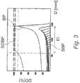
- Figure 11 shows the dose DO from non-modulated proton beams (pure Bragg peak BP) and modulated proton beams (spread-out Bragg peak SOBP). It also shows the sets of peaks SP, the amplitude of which is weighted. Figure 11 also indicates the interval EI of deposition of the energy of the spread-out peak.
- MLICs multilayer ionization chambers
- the principle that superintends use of the above apparatuses is the possibility of measuring the charge deposited on each of the anodes (or cathodes) of the various layers of the device while the beam of particles passes through a stack of calibrated water-equivalent absorbers. This enables instantaneous evaluation of the depth-dose distribution of the beam (whether single-energy beam or spread-out Bragg peaks) by virtue of the simultaneous reading of all the ionization chambers that make up the MLIC device.
- the typical structure of an MLIC is illustrated in Figure 1 .
- Figure 1 shows in this connection an MLIC sensor 10, which comprises a plurality of sensor structures, or channels, 20, in Figure 1 20 1 , ..., 20 N , comprising pairs 15 1 , ..., 15 N of anodes 11 and cathodes 12, separated by an ionization chamber 14, i.e., a space that identifies the ionization region, and followed by an absorber layer 13.
- MLIC sensor 10 which comprises a plurality of sensor structures, or channels, 20, in Figure 1 20 1 , ..., 20 N , comprising pairs 15 1 , ..., 15 N of anodes 11 and cathodes 12, separated by an ionization chamber 14, i.e., a space that identifies the ionization region, and followed by an absorber layer 13.
- the total number of channels identifies the maximum energy range of the particles that can be measured, whereas the materials and the physical thicknesses of each channel determine the water-equivalent thickness of the MLIC sensor 10.
- Known MLIC sensors comprise a fixed number of channels, for example 128 or 180 channels.
- Figure 2 illustrates an accelerator 1000, which is able to generate a beam of charged particles 1300 conveyed through a tunnel 1100 and an outlet mouth 1200 in the direction of a spatial region P, which in the figure is represented as being cylindrical of a length equal to the interval EI of deposition of the energy of the spread-out peak, even though in general it may assume also other shapes.
- This spatial region P is located, for example, above a therapy table 1400 on which a patient to be treated can be positioned.
- an apparatus for the calibration of beams of charged particles 100 is positioned in such a way that the beam of particles 1300 passes through MLIC sensors 20 that make up the calibration apparatus 100.
- This apparatus 100 is modular; i.e., it comprises a plurality of aligned sensor modules.
- the modular MLIC calibration apparatus 100 comprises an outer casing 110, of a substantially parallelepipedal shape, which comprises within it a horizontal stack of modular elements 120, each including an MLIC sensor 10, or another type of sensor for measuring the position and size of the beam of particles, and a supporting frame for the aforesaid sensor.
- the calibration apparatus 100 enables instantaneous evaluation of the characteristics of the therapeutic beam of particles 1300 in the directions X, Y, and Z, where Z corresponds to the direction along which the depth D is evaluated.
- ASIC Application-Specific Integrated Circuit
- Each channel circuit converts the input charge into an increment of a given number of counts of a purposely provided counter, where a fixed amount of charge, in what follows referred to as "quantum of charge", corresponds to the count of one.
- FIG. 4 A schematic representation of a channel circuit 205 is shown in Figure 4 .
- An input current i is integrated by means of an integrator circuit 201 comprising an operational transconductance amplifier (OTA) 202, an input resistance Rin connected to the inverting terminal of the OTA 202, and a capacitance Cint between the inverting terminal and the output of the OTA 202.
- An output voltage Vout of the integrator 201 at output from the OTA 202, increases when the input current i is negative, i.e., it comes out of the channel circuit 205, whereas it decreases otherwise.
- the output voltage Vout of the integrator 201 is compared with two fixed thresholds, a high one VTH and a low one VTL, via two synchronous comparators CMP_1 and CMP_2, the other input of which is connected to the output voltage Vout of the integrator 201.
- the threshold voltage of each of the two comparators CMP_1 and CMP_2 is set from outside: the high threshold voltage VTH is the voltage threshold of the first comparator CMP_1 that operates on negative input currents i, whereas the low threshold voltage VTL regards the comparator CMP_2, which is active for positive input currents.
- the value of the thresholds VTH and VTL does not have a particular influence on operation of the channel circuit 205 as long as the voltage variation remains within the output range of the OTA 202 and as long as the difference VTH-VTL between the two thresholds is greater than the voltage jump caused by subtraction of the charge quantum.
- the comparators CMP_1 and CMP_2 have their own outputs connected to two control inputs of a pulse generator PG. Appearing in Figure 4 is also a periodic clock signal clk, which provides a synchronisation reference both to the comparators CMP_1 and CMP_2 and to the pulse generator PG.
- the input node A of the OTA 202 is connected to a reference voltage VR, which is also the node on which the current pulse of polarity opposite to the one used for subtraction of charge is discharged, operating through two switches in series, a first switch sw1 and a second switch sw2.
- the reference voltage VR is a voltage that is connected to guard rings in the sensor to ensure that any possible charges that are not directly generated by ionization, but are for example generated by the difference of potential present between layers, are collected by the guard rings, without being transmitted to the layer on which the measurement signal (i.e., the current i) is picked up, which thus collects prevalently just the charges produced by ionization of the gas traversed by the beam of charged particles.
- the channel circuit 205 further comprises a charge-control capacitance Csub, one terminal of which is connected to the node identified between the first switch sw and the second switch sw2.
- the corresponding comparator CMP_1 or CMP_2 sets at its output a given logic level for the input of a pulse generator PG.
- the pulse generator PG sends to a capacitor Csub a positive pulse PC on its other terminal, as shown in Figure 5 .
- the voltage amplitude of the pulse PC, ⁇ Vpulse is defined as the difference between two reference voltages Vp+ and Vp-, which are set from outside.
- the total capacitance Csub may be obtained with three capacitors in parallel, of 50, 100, and 200 fF respectively, which may be added independently, so that the charge-control capacitance Csub can be selected with each value between 50 and 350 fF in steps of 50 fF, via a capacitance-selection signal Cap_sel.
- the output response of the capacitance Csub to a voltage pulse PC is represented by two current signals of opposite sign, ⁇ + and ⁇ -, associated to which are charges Q+ and Q-, respectively, according to the following relation (1):
- Q + Csub ⁇ ⁇ ⁇ Vpulse
- Q ⁇ Csub ⁇ ⁇ ⁇ Vpulse
- the timing of the first current signal ⁇ + is determined by the rising edge of the pulse PC, whereas the negative current signal ⁇ - corresponds to the falling edge of the pulse.
- the charge Q+ or Q- can be directed either to the input of the OTA 202 or else to the reference voltage VR, adding or subtracting a fixed amount of charge at each pulse P1, P2 generated by the pulse generator PG.
- the decision on which of the charge signals is to be sent to the OTA 202 depends upon the output of the comparators, in order to remove a fixed amount of charge from the capacitor Cint of the integrator. This results in a change in the voltage drop on the capacitor Cint, which is given by Q/Cint.
- Figure 5 shows a timing chart that represents the pulse PC sent to the capacitor Csub, the command pulses P1, P2 of the switches sw1, sw2, and the currents ⁇ + and ⁇ - in the switches.
- the pulse generator PG continues to emit pulses PC and stops when the voltage Vout passes again below (above) the threshold.
- the pulse generator PG sends a count pulse, which may be a signal for increment Cnt_Up or a signal for decrement Cnt_Down of the up/down counter 220, according to which is the comparator that is acting at its input.
- All the operations are synchronized via the external master clock clk and controlled via a digital finite-state machine (FSM) implemented in the generator block PG and not shown in Figure 4 .
- FSM digital finite-state machine
- the pulse generator PG detects that the comparator CMP_1 (or CMP_2) is active, the next two clock cycles are used for generating the pulses for charge subtraction and command of the switches sw1/sw2.
- Two supplementary clock cycles are required before reactivation of the FSM in the pulse generator PG in order to leave time for the OTA 202 to reduce the output voltage.
- five master-clock pulses are required.
- Reading of the total charge collected in the detector is provided by the number of counts generated during the measurement time multiplied by the value of the charge quantum Q c .
- Figure 6 shows a known solution of circuit arrangement, designated by 200, which envisages operating, for example, with a measurement apparatus 100 that has available a number M of channels 20 comprised in one or more MLIC sensors 10 arranged in a horizontal stack, as described with reference to Figure 2 .
- a sensor 10 of an MLIC type is provided purely by way of non-limiting example, it being possible for the sensor to be also of some other ionization-chamber type suitable for detecting the intensity of beams of charged particles and configured for sending its own measurement signal through a plurality of measurement channels 20, for example a pixel ionization-chamber detector.
- the circuit arrangement 200 comprises a number N equal to 64 of inputs in0, ..., in63, on each of which a channel 20 can be connected for conveying thereto a corresponding current i collected by the channel 20 of the MLIC sensor 10.
- Each of the above inputs in0, ..., in63 in the circuit arrangement 200 is the input of a respective circuit branch B0, ..., B63.
- Each k-th branch Bk comprises a channel conversion circuit 205 including a respective current-to-frequency converter 210, which converts the respective current i at input to the k-th branch into a frequency v k .
- This frequency v k is then measured by a counter 220, comprised in the k-th branch Bk, which supplies at output the value of the counter CT, in particular a 32-bit value.
- the values assumed by the counters CT0, ..., CT63 of the branches B0, ..., B63 are supplied as inputs to a multiplexer 250, which, upon command from a 6-bit selection bus CS, enables selection of the channel 20 from the channels connected to the inputs in0, ..., in63, i.e., of the branch from the branches B0, ..., B63, to be sent at its own output as output data O and to be acquired via a readout electronics 400 not shown in Figure 4 .
- the current-to-frequency converter implemented by the circuit arrangement 200 corresponds to a charge-to-count converter.
- the circuit arrangement 200 of Figure 4 also shown at input are the signals, supplied by an external controller, that have the function of controlling the channel circuits 205, hence the thresholds VTH, VTL of the comparators, the voltages VP+, VP-, the capacitance-selection signal Cap_sel, in addition to the signal on the selection bus CS of the chip and the selection circuits of the multiplexer 250.
- the circuit 200 moreover receives a latch signal, L, which has the function of loading at a given instant the output of the counters 220 into as many registers, and moreover an integrator-reset signal RA and a counter-reset signal RD.
- the integration capacitor Cint of each channel circuit 205 may in fact be discharged through a common digital reset input RA.
- all the counters 220 may be zeroed via a common reset asynchronous digital input, RD.
- the maximum current that a branch can convert before saturating is less than 24 ⁇ A.
- This value is too low for applications with pulsed accelerators, such as synchrocyclotrons.
- pulsed accelerators such as synchrocyclotrons.
- the instantaneous current during the pulse must reach values greater than those of current applications with linear accelerators, even by two or three orders of magnitude.
- the object of embodiments described herein is to improve the apparatuses and methods according to the known art as discussed previously.
- Various embodiments also refer to a corresponding measurement apparatus and method.
- the circuit arrangement proposed herein envisages providing, for a plurality of channels, a plurality of channel circuits comprising current-to-frequency converters and counters for supplying a respective channel count, stored in a respective channel register, as well as an adder-tree structure comprising at least one first column, or row, of adders that adds up the outputs of sets of channel registers, in particular comprising further columns of adders that add up the outputs, which are, in particular, stored in respective registers of the adders, of the adders of the previous column.
- the outputs of the channel registers and of each adder of each column are supplied to a multiplexer, which can in this way enable the channels necessary for detecting a given peak excursion without saturating.
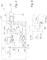
- Figure 7 shows an embodiment 500 of a circuit arrangement for acquisition of signals from an apparatus for calibration of beams of charged particles for external radiotherapy according to the invention.
- the architecture of the above circuit arrangement 500 comprises a plurality of branches BR0, ..., BR63 for the plurality of inputs in0, ..., in63, it being possible for each to be connected to a measurement channel 20 of an ionization-chamber sensor 10 in order to receive a respective measurement signal, in particular a current signal.
- Each k-th branch BRK comprises a channel circuit 205, like the one shown in Figure 4 , hence comprising a voltage-to-frequency converter 210 and a counter 220, as well as a channel register 230.
- the current-to-frequency converter implemented by the circuit arrangement 500 corresponds, in actual fact, to a charge-to-count converter.
- the adder structure 240 receives at input the outputs, or count values, CT0, ..., CT63, of the channel branches BR0, ..., BR63.
- Each channel branch BRk receives a measurement signal, in particular a current, at its input ink, determined by the connection to this input ink of the measurement channel 20, and supplies an output, i.e., a corresponding count CT.
- one measurement channel 20 can be connected to a number of inputs of the circuit arrangement 500; hence, an input ink may not receive the entire current of a channel 20.
- the adder structure 240 supplies at output sums of the measurement signals present at the inputs in0, ..., in63, or at a part of the inputs in0, ..., in63. In particular, the adder structure 240 supplies at output the data coming from sums of counts corresponding to the sum of:
- the multiplexer 550 in this way has 85 inputs: 64 inputs from the individual channels, 16 inputs as sum of four channel branches, 4 inputs as sum of 16 channel branches (sum of four which are sum of four) and one input as sum of all the channel branches (sum of four which are sum of sixteen), which is not shown in Figure 7 and is in part visible in Figure 8 .
- the adder structure 240 comprises an adder-tree structure including a first column 240 1 , or row, of adders 241 1 that adds up the outputs of sets of channel registers 230, specifically sets of four channel registers 230, and stores the result of the sum in a respective sum register 242 1 .
- the adder system 240 comprises further columns of adders 240 i , specifically, in the example, two further columns of adders 240 2 and 240 3 , which add up the outputs, in particular stored in the respective registers of the adders 242 i , of the adders 241 i-1 of the previous column 240 i-1 .
- the outputs of the sixteen registers 230 1 of the first column of the adders 241 1 are supplied four by four to the four adders 241 2 of the second column 240 2 .
- the outputs of the four registers 230 2 of the second column of the adders 241 2 are supplied to a single adder 241 3 of the third column 240 3 .
- the outputs of the first, second, and third column of adders are supplied to the multiplexer 550, which can, in this way, under the control of the selection signal 550, enable the channel branches necessary for detecting a given peak excursion without saturating.
- Figure 8 is a partial representation. In fact, it shows only the structure that, starting from the first four signals CT0, ..., CT3, generates the sum signal CT_100 at output from the adder 242 1 , as well as the path of the sum signal CT_100 in order to generate the sum signals CT_200 and CT-300, through subsequent adders 242 1 and 242 3 .
- the remaining direct signals CT0, ..., CT63 and sum signals CT_100, ..., CT_115, CT_200, ..., CT_203, CT_300 only the last signals CT63, CT_115, CT_203 are indicated in a schematic principle representation.
- the circuit arrangement 500 is hence used as follows: in the case where on a given channel 20 of a sensor 10 a current is expected such as to saturate the single branch Bk, for example a current with a value that is twice the saturation current that can be withstood by the single branch Bk, the channel 20 is connected in parallel to a plurality of branches; for example, the signal of a given channel 20 is connected to the branches B0, ..., B3 so that the current is divided on the four branches B0, ..., B3, thus preventing saturation of the channel circuits.
- the multiplexer 550 is configured for selecting, for the given channel 20, the output CT100 of the first column 240 1 of adders 241 1 .
- the circuit arrangement 200 comprises inputs in0, ..., in63 pre-arranged for being connected in sets of two or more at output from a measurement channel 20 that supplies a measurement signal i.
- This arrangement may take on, for example, the form of a simple electrical connection between the output of the measurement channel 20 and a set of the inputs in0, ..., ink, for example via an input terminal, or common node, connected at output from the measurement channel 20, departing from which are electrical cables or wires in parallel connected, either directly or via passive elements such as electrical resistances, to the respective inputs of the set.
- the cables or wires may, in particular, be connected manually, in so far as in general the measuring time does not entail the need to modify in an automated way the connections of the signals of the measurement channels 20 to the inputs in0, ..., ink of the circuit arrangement 200. It is, however, also possible to have, alternatively, a demultiplexer structure, which receives at input a measurement signal of one channel 20 and connects it, under the control of a respective control signal, governed for example by a computer, to a single input or else to two or more inputs in0, ..., ink in parallel.
- This control signal of the demultiplexer can hence be co-ordinated with the selection signal of the multiplexer 550 to connect simultaneously one measurement signal to a set of inputs and to select the output of the multiplexer corresponding to the sum of the set of branches BR0, ..., BRK corresponding to the set of inputs in0, ..., ink.
- a manual or automatic electrical connection arrangement for connecting a sensor channel 20 to a set of inputs of the plurality of inputs in0, ..., ink of the device 200.
- an apparatus for measurement of beams of charged particles for external radiotherapy, which comprises at least one sensor channel or measurement channel 20, the output of which is connected, in particular via a manual or automatic electrical connection arrangement, in parallel to at least one set of inputs in the plurality in0, ..., ink of the circuit arrangement 500 (or 200), and the multiplexer 550 is configured for selecting the outputs CT_100, ..., CT_115, or CT_200, ..., CT_203 or CT_300 of the adder structure 240 that adds up the values to the outputs CT0, ..., CT63 of the channel branches BR0, ..., BR63 corresponding to the set of inputs in0, ..., ink and for supplying them to the channel-readout circuit.
- the input resistance Rin on the channel circuit 205 is particularly useful.
- a measurement method that comprises connecting a given channel 20 of a sensor 10 to a respective branch or to a set of branches BR0, ..., BR63, in the example it being possible for the set to comprise four, sixteen, or sixty-four adjacent branches, of the circuit arrangement 500 that converges into one or more columns, in particular 240 1 , 240 2 , or 240 3 of adders 241 as a function of the value of a maximum current expected on that channel 20 of the sensor 10, configuring, via a 7-bit selection bus, the multiplexer 550 to select an output, corresponding to connection of that given channel 20, from among the direct outputs CT0, ..., CT63 of the channel branches BR0, ..., BR63 and the outputs CT_100, ..., CT_115, CT_200, ..., CT_203, CT_300 (i.e., the outputs of the respective sets of four, sixteen, and sixty-four adjacent branches) of the
- the operation of connecting a given channel 20 of a sensor 10 to a respective branch or to a set of branches of the circuit arrangement 500 comprises selecting for the connection a set of branches having a number of branches, in the example four, sixteen, or sixty-four, such as to divide on each branch a current lower than a saturation current of the channel circuit 205.
- Reading of the counters 230 can be carried out independently from any other operation.
- Figure 8 shows the circuit arrangement 500 in association with a further finite-state machine 260 of a Moore type that manages a loading signal L, which regulates storage of the 32-bit registers, i.e., the register 230 of the counter 220 and the registers 242 i of each i-th column 240 i of adders 241 i .
- the circuit 500 is shown only in part without the channel circuit 210. Consequently, for each k-th channel in k , signals ink_u and ink_d are represented that correspond to the count signals cnt_up and cnt_down of Figure 4 .
- the loading signal L is shifted synchronously with the clock clk: in the example illustrated in Figure 8 , first, after an initial state IN, at the first clock tick clk control of the FSM passes to a state L0, where the channel registers 230 connected to the counters 220 are loaded with the output, i.e., the total number counts CT thereof.
- Control in the finite-state machine 260 then returns to the initial state IN.
- the counters are stored in the registers all at the same time.
- the data in the registers 230 and 242 refer to the same time.
- Each register 230 and 242 of the circuit arrangement 500 has available a single bit of alarm signal that is activated when the most-significant bit of the counter (for a positive number and accordingly in two's complement for negative numbers), passes from 0 to 1.
- an OR logic that has as inputs all the signals corresponding to the various registers of the structure is equal to 1
- an operation of asynchronous reset can be used for unloading the registers in order to prevent overflow and hence loss of data.
- the OR gate collects the alarm signal of all the registers 230 and 242 and indicates that one of the registers has exceeded half of its maximum capacity. It then enables the readout electronics for sending a reset signal before overflow is reached.
- the circuit arrangement 500 described operates, for example, at a clock frequency of 400 MHz and at a maximum conversion rate of 80 MHz, the charge quantum Qc being selected in a range between 50 fC and 350 fC, thus enabling the limits of current of prior-art circuits to be overcome.
- circuit arrangement described thanks to the architecture that joins branches in parallel for each channel to an adder structure set between the branches and the multiplexer, enables the limits of current of known circuits to be overcome.
- the solution described herein makes it possible to obtain a uniform channel-to-channel relative gain, i.e., the gain of one channel with respect to the other, linearity over a wide dynamic range, and negligible background currents, as well as the possibility of managing a wider dynamic range of input currents, of the order of 10 4 .
- a technology with large scale of integration is used, 0.35- ⁇ m CMOS technology, in implementation of the ASIC, which enables installation of the chips in the proximity of the detector.
- the solution described herein can operate with inputs of both polarities, using 32-bit synchronous counters with up/down count capacity. In this way, the charge can be measured by counting the pulses at output from the channel converter in a given time interval.
- the output of the channel circuit is hence already in digital format, which enables a simpler subsequent management of the data.
- the circuit arrangement described operates at a clock frequency of 400 MHz and a maximum conversion rate of 80 MHz.
- the conversion of bipolar inputs makes it possible to extend the application of the circuit arrangement described to all the detectors that are used in the technical sector of calibration of beams of charged particles, and moreover enables a better precision in the measurement of low-current regimes (of the order of picoamps).
- the circuit arrangement described can operate with the ionization-chamber sensors that envisage channels arranged in a stack that develops along the direction of the beam, but can also operate with two-dimensional sensors, known as "pixel ionization-chamber detectors", which comprise an array of cells or pixels in the plane orthogonal to the beam, each of which corresponds to a channel and is hence designed to supply a current proportional to the dose that impinges on that cell or pixel, and in any case with all the ionization-chamber sensors suitable for detecting the intensity of beams of charged particles and configured for sending their own measurement signal through a plurality of measurement channels.
- pixel ionization-chamber detectors which comprise an array of cells or pixels in the plane orthogonal to the beam, each of which corresponds to a channel and is hence designed to supply a current proportional to the dose that impinges on that cell or pixel
Landscapes
- Health & Medical Sciences (AREA)
- Life Sciences & Earth Sciences (AREA)
- Physics & Mathematics (AREA)
- General Physics & Mathematics (AREA)
- High Energy & Nuclear Physics (AREA)
- Molecular Biology (AREA)
- Spectroscopy & Molecular Physics (AREA)
- Biomedical Technology (AREA)
- Engineering & Computer Science (AREA)
- Pathology (AREA)
- Nuclear Medicine, Radiotherapy & Molecular Imaging (AREA)
- Radiology & Medical Imaging (AREA)
- Animal Behavior & Ethology (AREA)
- General Health & Medical Sciences (AREA)
- Public Health (AREA)
- Veterinary Medicine (AREA)
- Measurement Of Radiation (AREA)
Claims (8)
- Schaltungsanordnung zur Erfassung von Signalen von einer Vorrichtung zur Messung der Strahlen geladener Teilchen in der externen Strahlentherapie, insbesondere Protonen, Kohlenstoffionen und andere lonenarten, die von Teilchenbeschleunigern emittiert werden, wobei die Schaltungsanordnung mindestens einen lonisationskammersensor (10) umfasst, wobei der mindestens eine Sensor (10) eine Vielzahl von Sensorkanälen (20) umfasst, die Schaltungsanordnung (200; 500) eine Vielzahl von parallelen Kanalzweigen (B0,.., B63; BR0, ..., BR63) umfasst, die dazu ausgelegt sind, mit den Sensorkanälen (20) verbunden zu werden, um jeweilige Messsignale (i) davon zu empfangen, wobei die Kanalzweige (B0, .., B63; BR0, ..., BR63) jeweils StromFrequenz-Wandler (210) und Zähler (220) umfassen, um Zählerwerte (220), die eine Ladung repräsentieren, die einem bestimmten Kanal (20) zugehörig ist, zu einem Multiplexer (250; 550) zu leiten, der in der Schaltungsanordnung (200; 500) enthalten ist,
wobei die Anordnung (200; 500) dadurch gekennzeichnet ist, dass
sie eine Addiererstruktur (240) mit mindestens einer ersten Spalte (2401) von Addierern (2411) umfasst, welche die Werte an den Ausgängen (CT0, ..., CT63) der Kanalzweige (BR0, ..., BR63) addiert, um Summenwerte (CT_100, ..., CT_115, CT_200, ..., CT_203, CT_300) an den Ausgängen davon bereitzustellen; und
die Schaltungsanordnung des Weiteren dazu konfiguriert ist, einen bestimmten Kanal (20) des Sensors (10) mit einem jeweiligen Kanalzweig oder einem Satz aus Kanalzweigen (BR0, ..., BR63) zu verbinden, der in die mindestens eine erste Spalte (2401) aus Addierern (2411) konvergiert, als eine Funktion des Wertes eines maximalen Stroms, der an dem Kanal (20) des Sensors (10) zu erwarten ist;
die Kanalzweige (BR0, ..., BR63) ihre eigenen Ausgaben (CT0, ..., CT63) direkt an den Multiplexer (550) und die Addiererstruktur (240) leiten, wobei der Multiplexer (550) dazu konfiguriert ist, aus den direkten Ausgaben (CT0, ..., CT63) der Kanalzweige (BR0, ..., BR63) und den Ausgaben (CT_100, ..., CT_115, CT_200, ..., CT_203, CT_300) der Addiererstruktur (240) ein Signal auszuwählen, das an Ausleseelektronik zum Auslesen (400) der Kanäle (200) geleitet werden soll. - Schaltungsanordnung nach Anspruch 1, dadurch gekennzeichnet, dass sie eine oder mehrere weitere Spalten (2401, 2402, 2403) von Addierern (241) umfasst, die Ausgaben der Addierer einer vorhergehenden Spalte addieren, um weitere Ausgaben der Addiererstruktur (240) zu bilden, die mit den Eingaben des Multiplexers (550) verbunden ist.
- Schaltungsanordnung nach Anspruch 1, dadurch gekennzeichnet, dass jeder Kanalzweig ein jeweiliges Kanalregister (230) umfasst, das zum Speichern des Zählerwertes (CT) des Zählers (220) angeschlossen ist, und jeder Addierer (241) einem jeweiligen Addiererregister (242) zum Speichern des Zählerwertes des Addierers (241) zugeordnet ist.
- Schaltungsanordnung nach Anspruch 3, dadurch gekennzeichnet, dass sie einen endlichen Automaten (260) umfasst, der dazu konfiguriert ist, die Daten in den Kanalregistern (230) und in den Registern (242) der Addierer der einzelnen Spalten (2401, 2402, 2403) synchron mit einem Taktsignal (clk) zu speichern, wobei die Daten bei jeder Zeitgabe des Taktsignals der Reihe nach in dem Kanalregister oder in jeder nachfolgenden Addiererspalte gespeichert werden.
- Schaltungsanordnung nach Anspruch 3 oder 4, dadurch gekennzeichnet, dass jedes Kanalregister (230) und jedes Addiererregister (242) über ein Alarmsignal verfügt, das aktiviert wird, wenn das höchstwertige Bit des Zählers auf eine hohe Stufe ansteigt, und eine Logikschaltung, die am Eingang jedes Signal von jedem Kanalregister (230) und jedem Addiererregister (242) empfängt und zum Überprüfen konfiguriert ist, ob alle Alarmsignale auf einer hohen Stufe sind und entsprechend einen Befehl auszugeben, insbesondere falls erforderlich, für einen Vorgang des asynchronen Zurücksetzens zum Entladen der Register (230, 242), um einen Überlaufzustand zu verhindern.
- Vorrichtung zur Messung von Strahlen geladener Teilchen (1300) in der externen Strahlentherapie, umfassend eine Schaltung zum Auslesen der Kanäle, umfassend eine Schaltungsanordnung nach einem der Ansprüche 1 bis 5.
- Verfahren zur Messung von Strahlen geladener Teilchen (1300) unter Verwendung der Messvorrichtung nach Anspruch 6, wobei die geladenen Teilchen insbesondere Protonen oder Ionen sind, die von Systemen für die externe Strahlentherapie mit geladenen Teilchen emittiert werden, dadurch gekennzeichnet, dass es folgende Schritte beinhaltet:Verbinden eines bestimmten Kanals (20) eines Sensors (10) mit einem jeweiligen Kanalzweig oder einem Satz aus Kanalzweigen (BR0, ..., BR63) der Schaltungsanordnung (500), der in eine oder mehrere Spalten aus Addierern (241) konvergiert, als eine Funktion des Wertes eines maximalen Stroms, der an dem Kanal (20) des Sensors (10) zu erwarten ist;wobei die Kanalzweige (BR0, ..., BR63) ihre eigenen Ausgaben (CT0, ..., CT63) direkt an den Multiplexer (550) und die Addiererstruktur (240) leiten,Konfigurieren des Multiplexers (550) zum Auswählen einer Ausgabe, entsprechend der Verbindung des bestimmten Kanals (20), aus den direkten Ausgaben (CT0, ..., CT63) der Kanalzweige (BR0, ..., BR63) und den Ausgaben (CT_100, ..., CT_115, CT_200, ..., CT_203, CT_3100) der Addiererstruktur (240) als ein Signal, das an eine Ausleseelektronik zum (400) Auslesen der Kanäle (20) geleitet werden soll.
- Verfahren nach Anspruch 7, dadurch gekennzeichnet, dass der Vorgang des Verbindens eines bestimmten Kanals (20) eines Sensors (10) mit einem jeweiligen Kanalzweig oder einem Satz aus Kanalzweigen (BR0, ..., BR63) der Schaltungsanordnung (500) das Auswählen, für die Verbindung, eines Satzes aus Zweigen (BR0, ..., BR63) mit einer Anzahl an Zweigen umfasst, um solcherart jedem Zweig einen Strom zuzuteilen, der niedriger als ein Sättigungsstrom der Kanalschaltung (205) ist.
Applications Claiming Priority (2)
| Application Number | Priority Date | Filing Date | Title |
|---|---|---|---|
| ITUB20151105 | 2015-06-10 | ||
| PCT/IB2016/053408 WO2016199067A1 (en) | 2015-06-10 | 2016-06-09 | Circuit arrangement for acquisition of signals from an apparatus for measuring beams of charged particles for external radiotherapy |
Publications (2)
| Publication Number | Publication Date |
|---|---|
| EP3308196A1 EP3308196A1 (de) | 2018-04-18 |
| EP3308196B1 true EP3308196B1 (de) | 2020-01-15 |
Family
ID=54150541
Family Applications (1)
| Application Number | Title | Priority Date | Filing Date |
|---|---|---|---|
| EP16744521.2A Active EP3308196B1 (de) | 2015-06-10 | 2016-06-09 | Schaltungsanordnung zur signalerfassung einer vorrichtung zur messung der strahlen geladener teilchen in der externen radiotherapie |
Country Status (3)
| Country | Link |
|---|---|
| US (1) | US10534093B2 (de) |
| EP (1) | EP3308196B1 (de) |
| WO (1) | WO2016199067A1 (de) |
Families Citing this family (6)
| Publication number | Priority date | Publication date | Assignee | Title |
|---|---|---|---|---|
| US10300304B2 (en) * | 2017-04-05 | 2019-05-28 | Pyramid Technical Consultants Inc. | Safety dose interlock for charged particle beams |
| US11933925B2 (en) | 2019-06-11 | 2024-03-19 | Bundesrepublik Deutschland, Vertreten Durch Das Bundesministerium Fur Wirtschaft Und Energie, Dieses Vertreten Durch Den Prasidenten Der Physikalisch-Technischen Bundesanstalt | Particle energy measuring device and method for determining a beam energy of a particle beam |
| KR102757413B1 (ko) * | 2019-11-29 | 2025-01-21 | 엘지전자 주식회사 | 방사선 디텍터 및 이를 이용한 방사선 촬영 방법 |
| JP6989834B2 (ja) * | 2020-05-07 | 2022-01-14 | 公益財団法人がん研究会 | 電位計の精度管理用電流発生装置、精度管理システム、及び校正方法 |
| IT202100019211A1 (it) * | 2021-07-20 | 2023-01-20 | Devices & Tech Torino S R L | Elettrodo sensore per rivelatori a ionizzazione e rivelatore a ionizzazione che lo incorpora |
| EP4224214A1 (de) * | 2022-02-04 | 2023-08-09 | Teledyne Dalsa B.V. | Energieauflösendes photonenzählungsdetektorpixel |
Family Cites Families (4)
| Publication number | Priority date | Publication date | Assignee | Title |
|---|---|---|---|---|
| US5619034A (en) * | 1995-11-15 | 1997-04-08 | Reed; David A. | Differentiating mass spectrometer |
| WO2006017333A2 (en) * | 2004-07-13 | 2006-02-16 | William Marsh Rice University | Shortened carbon nanotubes |
| FI119864B (fi) * | 2006-06-05 | 2009-04-15 | Planmeca Oy | Röntgenkuvantamissensori ja röntgenkuvantamismenetelmä |
| US8183910B2 (en) * | 2008-11-17 | 2012-05-22 | Taiwan Semiconductor Manufacturing Co., Ltd. | Circuit and method for a digital process monitor |
-
2016
- 2016-06-09 US US15/580,816 patent/US10534093B2/en active Active
- 2016-06-09 WO PCT/IB2016/053408 patent/WO2016199067A1/en not_active Ceased
- 2016-06-09 EP EP16744521.2A patent/EP3308196B1/de active Active
Non-Patent Citations (1)
| Title |
|---|
| None * |
Also Published As
| Publication number | Publication date |
|---|---|
| WO2016199067A1 (en) | 2016-12-15 |
| EP3308196A1 (de) | 2018-04-18 |
| US10534093B2 (en) | 2020-01-14 |
| US20180164445A1 (en) | 2018-06-14 |
Similar Documents
| Publication | Publication Date | Title |
|---|---|---|
| US10534093B2 (en) | Circuit arrangement for acquisition of signals from an apparatus for measuring beams of charged particles for external radiotherapy | |
| Werner et al. | Processing of prompt gamma-ray timing data for proton range measurements at a clinical beam delivery | |
| Aharrouche et al. | Energy linearity and resolution of the ATLAS electromagnetic barrel calorimeter in an electron test-beam | |
| JP5860590B2 (ja) | 放射線監視デバイス | |
| Vignati et al. | Beam monitors for tomorrow: the challenges of electron and photon FLASH RT | |
| US7964851B2 (en) | Method for the spectrometric photon dosimetry for X-ray and gamma radiation | |
| JP5345018B2 (ja) | 放射線分布検出回路 | |
| Curtis et al. | The construction and operation of a hybrid gas-silicon detector for studies of cluster breakup reactions | |
| US6348692B1 (en) | Device and method for nuclear locating by iterative computing of barycenter, and application to gamma-cameras | |
| Ray et al. | A trigger for the Fermilab E760 lead-glass calorimeter | |
| Akesson et al. | Electron identification with a prototype of the Transition Radiation Tracker for the ATLAS experiment: ATLAS TRT collaboration | |
| CN113711084B (zh) | 光子计数数据采集模块和用于光子计数的方法 | |
| Zhang et al. | First-ever deployment of a SiPM-on-tile calorimeter in a collider: a parasitic test with 200 GeV pp collisions at RHIC. | |
| Gallin-Martel et al. | Data read out and formatting for PMT-based rich detectors | |
| Presti et al. | Development of a scintillation-fiber detector for real-time particle tracking | |
| Kota et al. | Microdosimetric specification of the radiation quality of ad (48.5)+ Be fast neutron therapy beam produced by a superconducting cyclotron | |
| US9257156B2 (en) | Electromagnetic wave signal processor and electromagnetic wave detector | |
| Thornsberry | Proton Transfer Reactions Studied Using the Versatile Array of Neutron Detectors at Low Energy (VANDLE) | |
| Bahn Jr et al. | Decay of 20-Minute Ag 115 | |
| Reiter et al. | Measurement and simulation of the neutron response of the Nordball liquid scintillator array | |
| Watts et al. | Single and double $\delta $ production in the $^{3} $ He ($\gamma $, $\pi^{+}\pi $. sup (-)) reaction at 380 MeV $\leq $ E $ _ {\gamma} $$\leq $700 MeV | |
| Pierobon | Design and implementation of the Hybrid Detector for Microdosimetry (HDM): Challenges in readout architecture and experimental results | |
| Andreotti et al. | A fast and radiation-hard single-photon counting ASIC for the upgrade of the LHCb RICH detector at CERN | |
| Antonelli et al. | The electromagnetic calorimeter of the KLOE experiment at DAΦNE | |
| Billoud et al. | Radiation Field Study in ATLAS: Timepix measurements vs Geant4 simulations |
Legal Events
| Date | Code | Title | Description |
|---|---|---|---|
| STAA | Information on the status of an ep patent application or granted ep patent |
Free format text: STATUS: THE INTERNATIONAL PUBLICATION HAS BEEN MADE |
|
| PUAI | Public reference made under article 153(3) epc to a published international application that has entered the european phase |
Free format text: ORIGINAL CODE: 0009012 |
|
| STAA | Information on the status of an ep patent application or granted ep patent |
Free format text: STATUS: REQUEST FOR EXAMINATION WAS MADE |
|
| 17P | Request for examination filed |
Effective date: 20171207 |
|
| AK | Designated contracting states |
Kind code of ref document: A1 Designated state(s): AL AT BE BG CH CY CZ DE DK EE ES FI FR GB GR HR HU IE IS IT LI LT LU LV MC MK MT NL NO PL PT RO RS SE SI SK SM TR |
|
| AX | Request for extension of the european patent |
Extension state: BA ME |
|
| DAV | Request for validation of the european patent (deleted) | ||
| DAX | Request for extension of the european patent (deleted) | ||
| REG | Reference to a national code |
Ref country code: DE Ref legal event code: R079 Ref document number: 602016028323 Country of ref document: DE Free format text: PREVIOUS MAIN CLASS: G01T0001170000 Ipc: G01T0001290000 |
|
| RIC1 | Information provided on ipc code assigned before grant |
Ipc: G01T 1/29 20060101AFI20190605BHEP Ipc: G01T 1/17 20060101ALI20190605BHEP Ipc: G01T 1/185 20060101ALI20190605BHEP |
|
| GRAP | Despatch of communication of intention to grant a patent |
Free format text: ORIGINAL CODE: EPIDOSNIGR1 |
|
| STAA | Information on the status of an ep patent application or granted ep patent |
Free format text: STATUS: GRANT OF PATENT IS INTENDED |
|
| INTG | Intention to grant announced |
Effective date: 20190807 |
|
| GRAS | Grant fee paid |
Free format text: ORIGINAL CODE: EPIDOSNIGR3 |
|
| GRAA | (expected) grant |
Free format text: ORIGINAL CODE: 0009210 |
|
| STAA | Information on the status of an ep patent application or granted ep patent |
Free format text: STATUS: THE PATENT HAS BEEN GRANTED |
|
| AK | Designated contracting states |
Kind code of ref document: B1 Designated state(s): AL AT BE BG CH CY CZ DE DK EE ES FI FR GB GR HR HU IE IS IT LI LT LU LV MC MK MT NL NO PL PT RO RS SE SI SK SM TR |
|
| REG | Reference to a national code |
Ref country code: CH Ref legal event code: EP Ref country code: GB Ref legal event code: FG4D |
|
| REG | Reference to a national code |
Ref country code: IE Ref legal event code: FG4D |
|
| REG | Reference to a national code |
Ref country code: DE Ref legal event code: R096 Ref document number: 602016028323 Country of ref document: DE |
|
| REG | Reference to a national code |
Ref country code: CH Ref legal event code: PK Free format text: BERICHTIGUNGEN |
|
| REG | Reference to a national code |
Ref country code: AT Ref legal event code: REF Ref document number: 1225631 Country of ref document: AT Kind code of ref document: T Effective date: 20200215 |
|
| RAP2 | Party data changed (patent owner data changed or rights of a patent transferred) |
Owner name: INSTITUTO NAZIONALE DI FISICA NUCLEARE Owner name: DE.TEC.TOR S.R.L. Owner name: UNIVERSITA DEGLI STUDI DI TORINO |
|
| RIN2 | Information on inventor provided after grant (corrected) |
Inventor name: MAZZA, GIOVANNI Inventor name: FAUSTI, FEDERICO Inventor name: SACCHI, ROBERTO |
|
| REG | Reference to a national code |
Ref country code: NL Ref legal event code: MP Effective date: 20200115 |
|
| REG | Reference to a national code |
Ref country code: LT Ref legal event code: MG4D |
|
| PG25 | Lapsed in a contracting state [announced via postgrant information from national office to epo] |
Ref country code: PT Free format text: LAPSE BECAUSE OF FAILURE TO SUBMIT A TRANSLATION OF THE DESCRIPTION OR TO PAY THE FEE WITHIN THE PRESCRIBED TIME-LIMIT Effective date: 20200607 Ref country code: NL Free format text: LAPSE BECAUSE OF FAILURE TO SUBMIT A TRANSLATION OF THE DESCRIPTION OR TO PAY THE FEE WITHIN THE PRESCRIBED TIME-LIMIT Effective date: 20200115 Ref country code: RS Free format text: LAPSE BECAUSE OF FAILURE TO SUBMIT A TRANSLATION OF THE DESCRIPTION OR TO PAY THE FEE WITHIN THE PRESCRIBED TIME-LIMIT Effective date: 20200115 Ref country code: FI Free format text: LAPSE BECAUSE OF FAILURE TO SUBMIT A TRANSLATION OF THE DESCRIPTION OR TO PAY THE FEE WITHIN THE PRESCRIBED TIME-LIMIT Effective date: 20200115 Ref country code: NO Free format text: LAPSE BECAUSE OF FAILURE TO SUBMIT A TRANSLATION OF THE DESCRIPTION OR TO PAY THE FEE WITHIN THE PRESCRIBED TIME-LIMIT Effective date: 20200415 |
|
| REG | Reference to a national code |
Ref country code: CH Ref legal event code: NV Representative=s name: ISLER AND PEDRAZZINI AG, CH |
|
| PG25 | Lapsed in a contracting state [announced via postgrant information from national office to epo] |
Ref country code: BG Free format text: LAPSE BECAUSE OF FAILURE TO SUBMIT A TRANSLATION OF THE DESCRIPTION OR TO PAY THE FEE WITHIN THE PRESCRIBED TIME-LIMIT Effective date: 20200415 Ref country code: LV Free format text: LAPSE BECAUSE OF FAILURE TO SUBMIT A TRANSLATION OF THE DESCRIPTION OR TO PAY THE FEE WITHIN THE PRESCRIBED TIME-LIMIT Effective date: 20200115 Ref country code: SE Free format text: LAPSE BECAUSE OF FAILURE TO SUBMIT A TRANSLATION OF THE DESCRIPTION OR TO PAY THE FEE WITHIN THE PRESCRIBED TIME-LIMIT Effective date: 20200115 Ref country code: HR Free format text: LAPSE BECAUSE OF FAILURE TO SUBMIT A TRANSLATION OF THE DESCRIPTION OR TO PAY THE FEE WITHIN THE PRESCRIBED TIME-LIMIT Effective date: 20200115 Ref country code: GR Free format text: LAPSE BECAUSE OF FAILURE TO SUBMIT A TRANSLATION OF THE DESCRIPTION OR TO PAY THE FEE WITHIN THE PRESCRIBED TIME-LIMIT Effective date: 20200416 Ref country code: IS Free format text: LAPSE BECAUSE OF FAILURE TO SUBMIT A TRANSLATION OF THE DESCRIPTION OR TO PAY THE FEE WITHIN THE PRESCRIBED TIME-LIMIT Effective date: 20200515 |
|
| REG | Reference to a national code |
Ref country code: DE Ref legal event code: R097 Ref document number: 602016028323 Country of ref document: DE |
|
| PG25 | Lapsed in a contracting state [announced via postgrant information from national office to epo] |
Ref country code: ES Free format text: LAPSE BECAUSE OF FAILURE TO SUBMIT A TRANSLATION OF THE DESCRIPTION OR TO PAY THE FEE WITHIN THE PRESCRIBED TIME-LIMIT Effective date: 20200115 Ref country code: EE Free format text: LAPSE BECAUSE OF FAILURE TO SUBMIT A TRANSLATION OF THE DESCRIPTION OR TO PAY THE FEE WITHIN THE PRESCRIBED TIME-LIMIT Effective date: 20200115 Ref country code: DK Free format text: LAPSE BECAUSE OF FAILURE TO SUBMIT A TRANSLATION OF THE DESCRIPTION OR TO PAY THE FEE WITHIN THE PRESCRIBED TIME-LIMIT Effective date: 20200115 Ref country code: SM Free format text: LAPSE BECAUSE OF FAILURE TO SUBMIT A TRANSLATION OF THE DESCRIPTION OR TO PAY THE FEE WITHIN THE PRESCRIBED TIME-LIMIT Effective date: 20200115 Ref country code: SK Free format text: LAPSE BECAUSE OF FAILURE TO SUBMIT A TRANSLATION OF THE DESCRIPTION OR TO PAY THE FEE WITHIN THE PRESCRIBED TIME-LIMIT Effective date: 20200115 Ref country code: CZ Free format text: LAPSE BECAUSE OF FAILURE TO SUBMIT A TRANSLATION OF THE DESCRIPTION OR TO PAY THE FEE WITHIN THE PRESCRIBED TIME-LIMIT Effective date: 20200115 Ref country code: RO Free format text: LAPSE BECAUSE OF FAILURE TO SUBMIT A TRANSLATION OF THE DESCRIPTION OR TO PAY THE FEE WITHIN THE PRESCRIBED TIME-LIMIT Effective date: 20200115 Ref country code: LT Free format text: LAPSE BECAUSE OF FAILURE TO SUBMIT A TRANSLATION OF THE DESCRIPTION OR TO PAY THE FEE WITHIN THE PRESCRIBED TIME-LIMIT Effective date: 20200115 |
|
| REG | Reference to a national code |
Ref country code: AT Ref legal event code: MK05 Ref document number: 1225631 Country of ref document: AT Kind code of ref document: T Effective date: 20200115 |
|
| PLBE | No opposition filed within time limit |
Free format text: ORIGINAL CODE: 0009261 |
|
| STAA | Information on the status of an ep patent application or granted ep patent |
Free format text: STATUS: NO OPPOSITION FILED WITHIN TIME LIMIT |
|
| 26N | No opposition filed |
Effective date: 20201016 |
|
| PG25 | Lapsed in a contracting state [announced via postgrant information from national office to epo] |
Ref country code: AT Free format text: LAPSE BECAUSE OF FAILURE TO SUBMIT A TRANSLATION OF THE DESCRIPTION OR TO PAY THE FEE WITHIN THE PRESCRIBED TIME-LIMIT Effective date: 20200115 Ref country code: MC Free format text: LAPSE BECAUSE OF FAILURE TO SUBMIT A TRANSLATION OF THE DESCRIPTION OR TO PAY THE FEE WITHIN THE PRESCRIBED TIME-LIMIT Effective date: 20200115 |
|
| PG25 | Lapsed in a contracting state [announced via postgrant information from national office to epo] |
Ref country code: PL Free format text: LAPSE BECAUSE OF FAILURE TO SUBMIT A TRANSLATION OF THE DESCRIPTION OR TO PAY THE FEE WITHIN THE PRESCRIBED TIME-LIMIT Effective date: 20200115 Ref country code: SI Free format text: LAPSE BECAUSE OF FAILURE TO SUBMIT A TRANSLATION OF THE DESCRIPTION OR TO PAY THE FEE WITHIN THE PRESCRIBED TIME-LIMIT Effective date: 20200115 |
|
| PG25 | Lapsed in a contracting state [announced via postgrant information from national office to epo] |
Ref country code: LU Free format text: LAPSE BECAUSE OF NON-PAYMENT OF DUE FEES Effective date: 20200609 |
|
| PG25 | Lapsed in a contracting state [announced via postgrant information from national office to epo] |
Ref country code: IE Free format text: LAPSE BECAUSE OF NON-PAYMENT OF DUE FEES Effective date: 20200609 |
|
| PG25 | Lapsed in a contracting state [announced via postgrant information from national office to epo] |
Ref country code: TR Free format text: LAPSE BECAUSE OF FAILURE TO SUBMIT A TRANSLATION OF THE DESCRIPTION OR TO PAY THE FEE WITHIN THE PRESCRIBED TIME-LIMIT Effective date: 20200115 Ref country code: MT Free format text: LAPSE BECAUSE OF FAILURE TO SUBMIT A TRANSLATION OF THE DESCRIPTION OR TO PAY THE FEE WITHIN THE PRESCRIBED TIME-LIMIT Effective date: 20200115 Ref country code: CY Free format text: LAPSE BECAUSE OF FAILURE TO SUBMIT A TRANSLATION OF THE DESCRIPTION OR TO PAY THE FEE WITHIN THE PRESCRIBED TIME-LIMIT Effective date: 20200115 |
|
| PG25 | Lapsed in a contracting state [announced via postgrant information from national office to epo] |
Ref country code: MK Free format text: LAPSE BECAUSE OF FAILURE TO SUBMIT A TRANSLATION OF THE DESCRIPTION OR TO PAY THE FEE WITHIN THE PRESCRIBED TIME-LIMIT Effective date: 20200115 Ref country code: AL Free format text: LAPSE BECAUSE OF FAILURE TO SUBMIT A TRANSLATION OF THE DESCRIPTION OR TO PAY THE FEE WITHIN THE PRESCRIBED TIME-LIMIT Effective date: 20200115 |
|
| REG | Reference to a national code |
Ref country code: CH Ref legal event code: U11 Free format text: ST27 STATUS EVENT CODE: U-0-0-U10-U11 (AS PROVIDED BY THE NATIONAL OFFICE) Effective date: 20251124 |
|
| PGFP | Annual fee paid to national office [announced via postgrant information from national office to epo] |
Ref country code: DE Payment date: 20251126 Year of fee payment: 10 |
|
| PGFP | Annual fee paid to national office [announced via postgrant information from national office to epo] |
Ref country code: GB Payment date: 20251125 Year of fee payment: 10 |
|
| PGFP | Annual fee paid to national office [announced via postgrant information from national office to epo] |
Ref country code: IT Payment date: 20251110 Year of fee payment: 10 |
|
| PGFP | Annual fee paid to national office [announced via postgrant information from national office to epo] |
Ref country code: FR Payment date: 20251119 Year of fee payment: 10 |
|
| PGFP | Annual fee paid to national office [announced via postgrant information from national office to epo] |
Ref country code: BE Payment date: 20251124 Year of fee payment: 10 |
|
| PGFP | Annual fee paid to national office [announced via postgrant information from national office to epo] |
Ref country code: CH Payment date: 20251124 Year of fee payment: 10 |