EP3307024A1 - Organic el element - Google Patents
Organic el element Download PDFInfo
- Publication number
- EP3307024A1 EP3307024A1 EP16799581.0A EP16799581A EP3307024A1 EP 3307024 A1 EP3307024 A1 EP 3307024A1 EP 16799581 A EP16799581 A EP 16799581A EP 3307024 A1 EP3307024 A1 EP 3307024A1
- Authority
- EP
- European Patent Office
- Prior art keywords
- organic
- electroluminescent
- uneven structure
- cathode
- spatial frequency
- Prior art date
- Legal status (The legal status is an assumption and is not a legal conclusion. Google has not performed a legal analysis and makes no representation as to the accuracy of the status listed.)
- Granted
Links
- 238000000605 extraction Methods 0.000 claims abstract description 98
- 238000010521 absorption reaction Methods 0.000 claims abstract description 48
- 239000000758 substrate Substances 0.000 claims abstract description 46
- 238000000149 argon plasma sintering Methods 0.000 claims abstract description 41
- 230000001629 suppression Effects 0.000 claims abstract description 24
- 239000010419 fine particle Substances 0.000 claims description 21
- 238000000295 emission spectrum Methods 0.000 claims description 19
- 239000010410 layer Substances 0.000 description 110
- 238000001228 spectrum Methods 0.000 description 26
- 229920005989 resin Polymers 0.000 description 17
- 239000011347 resin Substances 0.000 description 17
- MCMNRKCIXSYSNV-UHFFFAOYSA-N Zirconium dioxide Chemical compound O=[Zr]=O MCMNRKCIXSYSNV-UHFFFAOYSA-N 0.000 description 12
- 238000000034 method Methods 0.000 description 12
- 239000000463 material Substances 0.000 description 11
- 230000009466 transformation Effects 0.000 description 11
- 230000000694 effects Effects 0.000 description 8
- 230000000052 comparative effect Effects 0.000 description 7
- 239000011521 glass Substances 0.000 description 7
- TVIVIEFSHFOWTE-UHFFFAOYSA-K tri(quinolin-8-yloxy)alumane Chemical compound [Al+3].C1=CN=C2C([O-])=CC=CC2=C1.C1=CN=C2C([O-])=CC=CC2=C1.C1=CN=C2C([O-])=CC=CC2=C1 TVIVIEFSHFOWTE-UHFFFAOYSA-K 0.000 description 7
- VYPSYNLAJGMNEJ-UHFFFAOYSA-N Silicium dioxide Chemical compound O=[Si]=O VYPSYNLAJGMNEJ-UHFFFAOYSA-N 0.000 description 6
- GWEVSGVZZGPLCZ-UHFFFAOYSA-N Titan oxide Chemical compound O=[Ti]=O GWEVSGVZZGPLCZ-UHFFFAOYSA-N 0.000 description 6
- 238000004364 calculation method Methods 0.000 description 6
- 230000004907 flux Effects 0.000 description 6
- 238000006243 chemical reaction Methods 0.000 description 5
- AMGQUBHHOARCQH-UHFFFAOYSA-N indium;oxotin Chemical compound [In].[Sn]=O AMGQUBHHOARCQH-UHFFFAOYSA-N 0.000 description 4
- 229920002799 BoPET Polymers 0.000 description 3
- BQCADISMDOOEFD-UHFFFAOYSA-N Silver Chemical compound [Ag] BQCADISMDOOEFD-UHFFFAOYSA-N 0.000 description 3
- 229910052782 aluminium Inorganic materials 0.000 description 3
- XAGFODPZIPBFFR-UHFFFAOYSA-N aluminium Chemical compound [Al] XAGFODPZIPBFFR-UHFFFAOYSA-N 0.000 description 3
- 238000004422 calculation algorithm Methods 0.000 description 3
- 229910052681 coesite Inorganic materials 0.000 description 3
- 229910052906 cristobalite Inorganic materials 0.000 description 3
- 230000007423 decrease Effects 0.000 description 3
- 238000010894 electron beam technology Methods 0.000 description 3
- 238000011156 evaluation Methods 0.000 description 3
- 238000004519 manufacturing process Methods 0.000 description 3
- IBHBKWKFFTZAHE-UHFFFAOYSA-N n-[4-[4-(n-naphthalen-1-ylanilino)phenyl]phenyl]-n-phenylnaphthalen-1-amine Chemical group C1=CC=CC=C1N(C=1C2=CC=CC=C2C=CC=1)C1=CC=C(C=2C=CC(=CC=2)N(C=2C=CC=CC=2)C=2C3=CC=CC=C3C=CC=2)C=C1 IBHBKWKFFTZAHE-UHFFFAOYSA-N 0.000 description 3
- 238000005424 photoluminescence Methods 0.000 description 3
- 239000002861 polymer material Substances 0.000 description 3
- 230000008569 process Effects 0.000 description 3
- 230000009467 reduction Effects 0.000 description 3
- 239000000377 silicon dioxide Substances 0.000 description 3
- 229910052682 stishovite Inorganic materials 0.000 description 3
- 229910052905 tridymite Inorganic materials 0.000 description 3
- VTYYLEPIZMXCLO-UHFFFAOYSA-L Calcium carbonate Chemical compound [Ca+2].[O-]C([O-])=O VTYYLEPIZMXCLO-UHFFFAOYSA-L 0.000 description 2
- 229920001609 Poly(3,4-ethylenedioxythiophene) Polymers 0.000 description 2
- 239000002042 Silver nanowire Substances 0.000 description 2
- 239000002313 adhesive film Substances 0.000 description 2
- TZCXTZWJZNENPQ-UHFFFAOYSA-L barium sulfate Chemical compound [Ba+2].[O-]S([O-])(=O)=O TZCXTZWJZNENPQ-UHFFFAOYSA-L 0.000 description 2
- 238000005266 casting Methods 0.000 description 2
- 230000008859 change Effects 0.000 description 2
- 238000005520 cutting process Methods 0.000 description 2
- 230000003247 decreasing effect Effects 0.000 description 2
- 238000009826 distribution Methods 0.000 description 2
- 238000007641 inkjet printing Methods 0.000 description 2
- 239000011159 matrix material Substances 0.000 description 2
- 239000007769 metal material Substances 0.000 description 2
- 239000002105 nanoparticle Substances 0.000 description 2
- 230000003287 optical effect Effects 0.000 description 2
- 239000004033 plastic Substances 0.000 description 2
- 229920003023 plastic Polymers 0.000 description 2
- 229920000139 polyethylene terephthalate Polymers 0.000 description 2
- 238000007639 printing Methods 0.000 description 2
- 230000005855 radiation Effects 0.000 description 2
- 238000009877 rendering Methods 0.000 description 2
- 238000005070 sampling Methods 0.000 description 2
- 239000002356 single layer Substances 0.000 description 2
- 238000004528 spin coating Methods 0.000 description 2
- 229920001187 thermosetting polymer Polymers 0.000 description 2
- XOLBLPGZBRYERU-UHFFFAOYSA-N tin dioxide Chemical compound O=[Sn]=O XOLBLPGZBRYERU-UHFFFAOYSA-N 0.000 description 2
- 238000007740 vapor deposition Methods 0.000 description 2
- GEIAQOFPUVMAGM-UHFFFAOYSA-N ZrO Inorganic materials [Zr]=O GEIAQOFPUVMAGM-UHFFFAOYSA-N 0.000 description 1
- 239000000853 adhesive Substances 0.000 description 1
- 230000001070 adhesive effect Effects 0.000 description 1
- PNEYBMLMFCGWSK-UHFFFAOYSA-N aluminium oxide Inorganic materials [O-2].[O-2].[O-2].[Al+3].[Al+3] PNEYBMLMFCGWSK-UHFFFAOYSA-N 0.000 description 1
- 238000004458 analytical method Methods 0.000 description 1
- 238000013459 approach Methods 0.000 description 1
- 230000004888 barrier function Effects 0.000 description 1
- 230000015572 biosynthetic process Effects 0.000 description 1
- 229910000019 calcium carbonate Inorganic materials 0.000 description 1
- 239000002131 composite material Substances 0.000 description 1
- 239000000470 constituent Substances 0.000 description 1
- 238000011109 contamination Methods 0.000 description 1
- 229910052593 corundum Inorganic materials 0.000 description 1
- 238000013461 design Methods 0.000 description 1
- 230000006866 deterioration Effects 0.000 description 1
- 238000010438 heat treatment Methods 0.000 description 1
- 238000007654 immersion Methods 0.000 description 1
- 230000006872 improvement Effects 0.000 description 1
- 230000031700 light absorption Effects 0.000 description 1
- 239000007788 liquid Substances 0.000 description 1
- 238000005259 measurement Methods 0.000 description 1
- 239000000203 mixture Substances 0.000 description 1
- 238000013041 optical simulation Methods 0.000 description 1
- 239000011368 organic material Substances 0.000 description 1
- 230000003647 oxidation Effects 0.000 description 1
- 238000007254 oxidation reaction Methods 0.000 description 1
- NRNCYVBFPDDJNE-UHFFFAOYSA-N pemoline Chemical compound O1C(N)=NC(=O)C1C1=CC=CC=C1 NRNCYVBFPDDJNE-UHFFFAOYSA-N 0.000 description 1
- 230000000737 periodic effect Effects 0.000 description 1
- 229920002120 photoresistant polymer Polymers 0.000 description 1
- 229920000172 poly(styrenesulfonic acid) Polymers 0.000 description 1
- 238000006116 polymerization reaction Methods 0.000 description 1
- 229940005642 polystyrene sulfonic acid Drugs 0.000 description 1
- 238000003825 pressing Methods 0.000 description 1
- 239000010703 silicon Substances 0.000 description 1
- 229910052710 silicon Inorganic materials 0.000 description 1
- 229910052709 silver Inorganic materials 0.000 description 1
- 239000004332 silver Substances 0.000 description 1
- 238000004088 simulation Methods 0.000 description 1
- 239000000243 solution Substances 0.000 description 1
- 230000003595 spectral effect Effects 0.000 description 1
- 239000000126 substance Substances 0.000 description 1
- 229910052623 talc Inorganic materials 0.000 description 1
- 238000012360 testing method Methods 0.000 description 1
- 229920005992 thermoplastic resin Polymers 0.000 description 1
- 238000012546 transfer Methods 0.000 description 1
- XLYOFNOQVPJJNP-UHFFFAOYSA-N water Substances O XLYOFNOQVPJJNP-UHFFFAOYSA-N 0.000 description 1
- 238000004804 winding Methods 0.000 description 1
- 229910001845 yogo sapphire Inorganic materials 0.000 description 1
- YVTHLONGBIQYBO-UHFFFAOYSA-N zinc indium(3+) oxygen(2-) Chemical compound [O--].[Zn++].[In+3] YVTHLONGBIQYBO-UHFFFAOYSA-N 0.000 description 1
- XLOMVQKBTHCTTD-UHFFFAOYSA-N zinc oxide Inorganic materials [Zn]=O XLOMVQKBTHCTTD-UHFFFAOYSA-N 0.000 description 1
- 239000011787 zinc oxide Substances 0.000 description 1
Images


Classifications
-
- H—ELECTRICITY
- H10—SEMICONDUCTOR DEVICES; ELECTRIC SOLID-STATE DEVICES NOT OTHERWISE PROVIDED FOR
- H10K—ORGANIC ELECTRIC SOLID-STATE DEVICES
- H10K50/00—Organic light-emitting devices
- H10K50/80—Constructional details
- H10K50/805—Electrodes
- H10K50/82—Cathodes
- H10K50/822—Cathodes characterised by their shape
-
- H—ELECTRICITY
- H10—SEMICONDUCTOR DEVICES; ELECTRIC SOLID-STATE DEVICES NOT OTHERWISE PROVIDED FOR
- H10K—ORGANIC ELECTRIC SOLID-STATE DEVICES
- H10K50/00—Organic light-emitting devices
- H10K50/80—Constructional details
- H10K50/85—Arrangements for extracting light from the devices
- H10K50/854—Arrangements for extracting light from the devices comprising scattering means
-
- G—PHYSICS
- G02—OPTICS
- G02B—OPTICAL ELEMENTS, SYSTEMS OR APPARATUS
- G02B5/00—Optical elements other than lenses
- G02B5/02—Diffusing elements; Afocal elements
-
- H—ELECTRICITY
- H10—SEMICONDUCTOR DEVICES; ELECTRIC SOLID-STATE DEVICES NOT OTHERWISE PROVIDED FOR
- H10K—ORGANIC ELECTRIC SOLID-STATE DEVICES
- H10K50/00—Organic light-emitting devices
- H10K50/80—Constructional details
- H10K50/805—Electrodes
- H10K50/81—Anodes
- H10K50/813—Anodes characterised by their shape
-
- H—ELECTRICITY
- H10—SEMICONDUCTOR DEVICES; ELECTRIC SOLID-STATE DEVICES NOT OTHERWISE PROVIDED FOR
- H10K—ORGANIC ELECTRIC SOLID-STATE DEVICES
- H10K50/00—Organic light-emitting devices
- H10K50/80—Constructional details
- H10K50/805—Electrodes
- H10K50/82—Cathodes
-
- H—ELECTRICITY
- H10—SEMICONDUCTOR DEVICES; ELECTRIC SOLID-STATE DEVICES NOT OTHERWISE PROVIDED FOR
- H10K—ORGANIC ELECTRIC SOLID-STATE DEVICES
- H10K50/00—Organic light-emitting devices
- H10K50/80—Constructional details
- H10K50/85—Arrangements for extracting light from the devices
-
- H—ELECTRICITY
- H10—SEMICONDUCTOR DEVICES; ELECTRIC SOLID-STATE DEVICES NOT OTHERWISE PROVIDED FOR
- H10K—ORGANIC ELECTRIC SOLID-STATE DEVICES
- H10K50/00—Organic light-emitting devices
- H10K50/80—Constructional details
- H10K50/85—Arrangements for extracting light from the devices
- H10K50/858—Arrangements for extracting light from the devices comprising refractive means, e.g. lenses
Definitions
- the present invention relates to an organic EL (electroluminescent) device which effectively alleviates surface plasmon absorption at a cathode and has improved light extraction efficiency.
- a general organic EL (electroluminescent) device has only 20 % light extraction efficiency from a transparent substrate into the air. Accordingly, considering mass productivity and the like, an external film is attached to the device in many cases. Although it depends on the device structure, the light extraction efficiency is about 30% even when an external film is attached to the organic EL (electroluminescent) device, and loss of light is large.
- a light scattering structure is being considered in order to alleviate total reflection due to the difference in refractive index between the transparent substrate and the transparent electrode.
- the light scattering structure alleviates the total reflection of light and allows more light to be extracted.
- the light extraction efficiency of an organic EL (electroluminescent) device having a light scattering structure is only about 40 %.
- the surface of the cathode part has a two-dimensional lattice structure in which a plurality of recesses are arranged at a certain interval in two dimensions.
- This two-dimensional lattice structure functions as a diffraction grating and converts the surface plasmons generated by light at the cathode into light again, thereby improving light extraction efficiency.
- Light can be efficiently extracted by setting the interval of the two-dimensional lattice structure at an interval that is optimum for conversion of surface plasmons to light.
- such two-dimensional lattice structures limit the direction in which light is efficiently extracted in the two-dimensional plane by the direction in which the plurality of recesses in the structure are arranged.
- the interval of the two-dimensional lattice structure is not optimum for conversion of surface plasmons to light, and light cannot be extracted efficiently.
- the present invention has been devised to solve such problems, and an object thereof is to effectively alleviate surface plasmon absorption at the cathode of an organic EL (electroluminescent) device and improve the light extraction efficiency.
- An organic EL (electroluminescent) device of a first aspect of the present invention includes a translucent substrate having a first surface and a second surface; a transparent electrode, a cathode, and a luminescent layer provided between the transparent electrode and the cathode which are formed over the first surface; and a light extraction film having unevenness placed on the second surface, wherein the cathode has a plurality of recesses or protrusions on the surface thereof facing the luminescent layer, and the Fourier transform image of the surface of the cathode facing the luminescent layer includes one or more surface plasmon absorption suppression areas including a spatial frequency ⁇ obtained by Equation (I) and one or more light scattering areas not including a spatial frequency that is equal to or greater than the spatial frequency v.
- ⁇ 1 is the relative permittivity of the luminescent layer
- ⁇ 2 is the relative permittivity of the cathode
- Re() is a function for extracting the real part of a complex number
- ⁇ is the central wavelength of the emission spectrum of the luminescent layer
- An organic EL (electroluminescent) device of a second aspect of the present invention is characterized in that, in the organic EL (electroluminescent) device of the first aspect, the one or more surface plasmon absorption suppression areas include spatial frequencies ⁇ that are ⁇ 1 or greater to ⁇ 2 or less, and the one or more light scattering areas do not include spatial frequencies ⁇ that are ⁇ 1 or greater to ⁇ 2 or less.
- ⁇ 1 and ⁇ 2 are obtained by, assuming that ⁇ p represents the peak wavelength of the emission spectrum of the luminescent layer, S( ⁇ ) represents the intensity at the wavelength ⁇ , ⁇ min represents the minimum wavelength that satisfies S( ⁇ ) > S( ⁇ p )/100, ⁇ max represents the maximum wavelength that satisfies S( ⁇ ) > S ( ⁇ p )/100, and k represents a real number larger than 0.8, substituting ⁇ 1 and ⁇ 2 obtained from Equation (II) and Equation (III) to ⁇ of Equation (I).
- An organic EL (electroluminescent) device of a third aspect of the present invention is characterized in that, in the organic EL (electroluminescent) device of the first aspect, the emission spectrum of the luminescent layer has a plurality of emission peak wavelengths ⁇ p1 ... ⁇ pn , and the surface plasmon absorption suppression area includes spatial frequencies ⁇ p1 ... v pn obtained by substituting ⁇ p1 ... ⁇ pn to ⁇ of Equation (I).
- An organic EL (electroluminescent) device of a fourth aspect of the present invention is characterized in that, in the organic EL (electroluminescent) devices of the first to third aspects, an uneven structure layer having a plurality of protrusions or recesses is further included, and the uneven structure layer, the transparent electrode, the luminescent layer, and the cathode are stacked in this order on the first surface of the translucent substrate.
- An organic EL (electroluminescent) device of a fifth aspect of the present invention is characterized in that, in the organic EL (electroluminescent) device of the fourth aspect, the refractive index of the uneven structure layer is 1.7 or greater.
- An organic EL (electroluminescent) device of a sixth aspect of the present invention is characterized in that, in the organic EL (electroluminescent) device of the fourth aspect, the uneven structure layer includes light scattering fine particles.
- An organic EL (electroluminescent) device of a seventh aspect of the present invention is characterized in that, in the organic EL (electroluminescent) device of the fourth aspect, a prism structure is further included, and the prism structure is provided between the translucent substrate and the uneven structure layer, and the refractive index of the prism structure is 1.7 or less.
- An organic EL (electroluminescent) device of a eighth aspect of the present invention is characterized in that, in the organic EL (electroluminescent) device of the fourth aspect, the plurality of protrusions or recesses of the uneven structure layer have an in-plane dimension of 1 mm or less.
- the organic EL (electroluminescent) device of the first aspect of the present invention provides a high light extraction efficiency by including, on the surface of the cathode, an uneven structure having a spatial frequency that is effective for suppressing surface plasmon absorption corresponding to the light extraction easy direction of the uneven light extraction film, and an uneven structure having a spatial frequency effective for scattering light corresponding to the light extraction difficult direction of the uneven light extraction film.
- the organic EL (electroluminescent) device of the second aspect of the present invention adapts the spatial frequency of the uneven structure having a spatial frequency that is effective for suppressing surface plasmon absorption of the cathode to the emission spectrum of the luminescent layer so that the surface plasmon absorption at the surface of the cathode can be more efficiently suppressed.
- the organic EL (electroluminescent) device of the third aspect of the present invention sets the spatial frequency for suppressing surface plasmon absorption of the cathode in accordance with the luminescent layer having a plurality of emission wavelength peaks so that change in the distribution of the emission spectrum can be reduced, and at the same time the surface plasmon absorption at the surface of the cathode can be more efficiently suppressed.
- the organic EL (electroluminescent) device of the fourth aspect of the present invention introduces an uneven structure to, in addition to the surface of the cathode, the anode and the luminescent layer so as to enhance the light scattering property at the interface thereof and realize a higher light extraction efficiency.
- the organic EL (electroluminescent) device of the fifth aspect of the present invention realizes a higher light extraction efficiency by suppressing the total reflection at the interface between the uneven structure layer and the anode.
- the organic EL (electroluminescent) device of the sixth aspect of the present invention realizes a higher light extraction efficiency by scattering light in the uneven structure layer and suppressing the total reflection at the interface between the translucent substrate and the air.
- the organic EL (electroluminescent) device of the seventh aspect of the present invention realizes a higher light extraction efficiency by suppressing the total reflection at the interface between the uneven structure layer and the translucent substrate.
- the organic EL (electroluminescent) device of the eighth aspect of the present invention makes it possible to maintain good appearance during operation even when leak spots are generated by limiting their dimension to a range of 1 mm or less.
- a structure for scattering light is provided on the surface of the translucent substrate facing the air, 1) total reflection at the interface between the translucent substrate and the air can be suppressed. Further, if a structure for scattering light is provided on the side of the translucent substrate facing the transparent electrode, 2) total reflection at the interface between the transparent electrode and the translucent substrate can be suppressed. As for 3) surface plasmon absorption at the cathode, it is known to suppress loss of light due to surface plasmon absorption by providing an uneven structure on the cathode.
- Fig. 1 shows a configuration example of a top emission type organic EL (electroluminescent) device in which an uneven structure layer 20, a cathode 30, a luminescent layer 40, and an anode (transparent electrode) 50 are stacked in this order on a substrate 10 and a translucent substrate 60 is provided on the anode 50.
- Fig. 2 shows a configuration example of a bottom emission type organic EL (electroluminescent) device in which an uneven structure layer 20, an anode (transparent electrode) 50, a luminescent layer 40, and a cathode (30 are stacked in this order on a translucent substrate 60.
- Figs. 1 shows a configuration example of a top emission type organic EL (electroluminescent) device in which an uneven structure layer 20, a cathode 30, a luminescent layer 40, and an anode (transparent electrode) 50 are stacked in this order on a substrate 10 and a translucent substrate 60 is provided on the anode 50.
- an uneven structure is formed on the surface of the cathode 30 facing the luminescent layer 40 in such a manner that it matches with the uneven structure on the surface of the uneven structure layer 20.
- the uneven structure layer 20 since the uneven structure layer 20 is provided, the uneven structure is also introduced into the anode and the luminescent layer in addition to the surface of the cathode 30. The introduction of the uneven structure enhances the light scattering at the interface between those layers and enables a higher light extraction efficiency.
- the translucent substrate 60 is required to be highly transparent and also to be a sufficient barrier in order to prevent deterioration of the luminescent layer 40.
- the translucent substrate 60 is a glass substrate, although it is not limited to this.
- Materials for forming the translucent substrate 60 may include glass, various plastics, and silicon.
- the translucent substrate 60 may be a single layer or a laminated structure including a plurality of layers.
- the translucent substrate 60 has a thickness of 0.1 mm to 1 mm.
- the uneven structure layer 20 can be formed using a thermosetting resin, an oxidation polymerization resin, a reaction curable resin, an ultraviolet curable resin, an electron beam curable resin, a thermoplastic resin, or the like. In order to facilitate formation of the uneven structure, preferably, an ultraviolet curable resin or an electron beam curable resin is used. Alternatively, the uneven structure layer 20 may be formed using the so-called "positive type" photoresist whose solubility to a developer increases at parts irradiated with actinic radiation such as ultraviolet radiation.
- the anode 50 is formed using a material having high transparency and conductivity.
- the anode 50 may be made of an inorganic conductive film such as indium tin oxide (ITO), indium zinc oxide (IZO), ZnO, Cul, and SnO 2 , an organic conductive film such as a mixture of polyethylene dioxythiophene and polystyrene sulfonic acid (PEDOT/PSS), or a composite conductive film such as a silver nanowire ink formed by dispersing silver nanowires in a polymer material, but it is not limited to these.
- the anode 50 can be formed by any method known in the art, such as vapor deposition, spin coating, casting, ink jetting, and printing.
- the luminescent layer 40 is formed using an arbitrary low molecular weight material and/or an arbitrary polymer material known in the art.
- the luminescent layer 40 may be a single layer or a laminated structure including a plurality of layers, provided that it includes at least one layer having a luminescent function ("luminescent layer" in the narrow sense).
- the luminescent layer 40 may include a hole injecting layer, a hole transporting layer, an electron transporting layer, and/or an electron injecting layer in addition to the luminescent layer in the narrow sense.
- the luminescent layer 40 can be formed by any method known in the art, such as vapor deposition, spin coating, casting, ink jetting, and printing.
- the cathode 30 is formed using a reflective metal material.
- Reflective metal materials that can be used include aluminum, silver, and the like.
- Fig. 3A shows a top view of a prior art cathode with a periodically arranged uneven structure.
- the protrusions are shown in black, and the recesses are shown in white. Even if the black parts are protrusions and the white parts are recesses, a similar optical effect can be obtained.
- the recesses of Fig. 3A have a quadrangular shape and are periodically arranged in a staggered manner.
- recesses or protrusions having another shape such as a circle, an ellipse, and a polygon may by periodically arranged and still provide the effect of suppressing loss of light due to surface plasmon absorption.
- the recesses or protrusions may be arranged in a square matrix without being staggered. Alternatively, a slight randomness may be imparted to the above-mentioned staggered array or square matrix array.
- Such a periodic uneven structure has some effects on suppressing surface plasmon absorption.
- the Fourier transform of the structure of Fig. 3A is calculated, resulting in the two-dimensional frequency spectrum of Fig. 3B .
- F(u, v) is determined by the following equation using the spatial frequency component in the x-axis direction u and the spatial frequency component in the y-axis direction v.
- the larger the number of samples in the x direction M and the number of samples in the y direction N the more accurately the structure can be represented.
- the interval of the sampling points is set to be not greater than half of the unit frequency width.
- the array of recesses indicated by line 100a in Fig. 3A has periodicity in the direction indicated by line 102a and a spatial frequency in the direction indicated by line 104a in Fig. 3B .
- the array of recesses indicated by line 100b in Fig. 3A has periodicity in the direction indicated by line 102b and a spatial frequency in the direction indicated by line 104b in Fig. 3B .
- the uneven structure of Fig. 3A has periodicity in the directions from the center to the bright points in the image of Fig. 3B .
- the directions effective for suppressing surface plasmon absorption are only those directions in which the uneven structure has periodicity, and only those directions connecting the center and the bright spots of the image in Fig. 3B .
- Figs. 6A, 6B , 7A, and 7B show typical structures of uneven light extraction films.
- Figs. 6A and 6B show a top view and a cross-sectional view of an uneven light extraction film provided with hemispherical protrusions 92 on a transparent support 90.
- Figs. 7A and 7B show a top view and a cross-sectional view of an uneven light extraction film provided with quadrangular pyramid recesses 92 on a transparent support 90.
- configuration examples in which protrusions or recesses are arranged regularly are shown. However, the protrusions or recesses may be randomly arranged.
- a flat surface is likely to cause total reflection at the interface between the transparent support 90 and the air and produce loss of light.
- the light extraction efficiency can be improved by providing an uneven form like those shown in Figs. 6A, 6B , 7A, and 7B .
- the shape and arrangement of the protrusions or recesses can be changed variously. However, depending on the shape and/or arrangement, there may be directions in which light extraction is easy and directions in which light extraction is difficult.
- a flat surface is inevitably produced, and the light extraction efficiency becomes lower than that of the configuration example in which quadrangular pyramid recesses are arranged as shown in Figs. 7A and 7B .
- FIG. 8A shows directions 122 in which light extraction is easy and directions 124 in which light extraction is difficult of the configuration example in which hemispherical protrusions are arranged shown in Figs. 6A and 6B .
- Fig. 8B shows directions 122 in which light extraction is easy and directions 124 in which light extraction is difficult of the configuration example in which quadrangular pyramid recesses are arranged shown in Figs. 7A and 7B .
- Figs. 9A and 9B show the behavior of light in the case where hemispherical protrusions are provided as shown in Figs. 6A and 6B .
- Fig. 9A shows a cross section along the direction 122 in which light extraction is easy. In this cross section, light emitted under suppressed surface plasmon absorption by the unevenness of the cathode can be extracted to the outside by passing through the hemispherical protrusion 92.
- Fig. 9B shows a cross section along the direction 124 in which light extraction is difficult. In this cross section, the density of the hemispherical protrusions 92 is small, and the probability of total reflection at the flat surface of the transparent support 90 increases. Thus, even if the surface plasmon absorption is suppressed by the unevenness of the cathode, the efficiency of extracting light emitted from the luminescent layer to the outside is reduced.
- the directions 122 in which light extraction is easy and the directions 124 in which light extraction is difficult of the uneven light extraction film can be determined by measuring the orientation angle of the external emitted light of the organic EL (electroluminescent) device using a spectral radiance meter (for example, TOPCON-SR3AR manufactured by TOPCON TECHNOHOUSE CO., LTD.).
- a spectral radiance meter for example, TOPCON-SR3AR manufactured by TOPCON TECHNOHOUSE CO., LTD.
- the orientation angle of the light inside the organic EL (electroluminescent) device is measured by bringing the cylindrical lens into close contact with the surface of the transparent support 90 where there is no uneven structure and measuring the orientation angle.
- a liquid with a refractive index that is close to that of the materials of the transparent support 90 and the cylindrical lens is used (for example, 1.52 in case of glass).
- the orientation angle of light extracted to the outside is measured by attaching the uneven light extraction film having the uneven structure to the surface of the transparent support and measuring the orientation angle. Comparing the orientation angles of the internal light and external light, the directions 122 in which light extraction is easy and the directions 124 in which light extraction is difficult can be determined. Alternatively, the directions 122 in which light extraction is easy and the directions 124 in which light extraction is difficult direction may be determined by ray tracing optical simulation. In this case, both directions can be determined without performing the above-described measurement.
- the organic EL (electroluminescent) device of the present invention includes a translucent substrate having a first surface and a second surface; a transparent electrode, a cathode, and a luminescent layer provided between the transparent electrode and the cathode which are formed over the first surface; and a light extraction film having unevenness placed on the second surface, wherein the cathode has a plurality of recesses or protrusions on the surface thereof facing the luminescent layer, and the Fourier transform image of the surface of the cathode facing the luminescent layer includes one or more surface plasmon absorption suppression areas including a spatial frequency ⁇ obtained by Equation (I) and one or more light scattering areas not including a spatial frequency that is equal to or greater than the spatial frequency ⁇ .
- an "area including the spatial frequency ⁇ " indicates that, for all of the spatial frequencies ⁇ in that area, the value of F(u, v) is no less than a threshold Th.
- An "area not including the spatial frequency ⁇ " indicates that, for all of the spatial frequencies ⁇ in that area, the value of F(u, v) is smaller than the threshold Th.
- the threshold Th may be 10 % or greater, preferably 50 % or greater of the maximum value of F(u, v) in the entire Fourier transform image.
- Fig. 10 One example of the Fourier transform image of the cathode of the present invention is shown in Fig. 10 .
- Four areas that are not adjacent to each other are surface plasmon absorption suppression areas 142 including the spatial frequency ⁇ obtained from Equation (I).
- the other four areas are light scattering areas 144 which do not include spatial frequencies equal to or greater than the spatial frequency ⁇ obtained from Equation (I).
- the spatial frequency represented by the surface plasmon absorption suppression area 142 is used as the spatial frequency of the uneven structure in the direction 122 in which light extraction is easy of the uneven light extraction film, so that, as shown in Fig.
- the spatial frequency represented by the light scattering area 144 is used as the spatial frequency of the uneven structure in the direction 124 in which light extraction is difficult of the uneven light extraction film, so that, as shown in Fig. 11B , light emitted from the luminescent layer and reflected at the cathode is scattered, whereby total reflection at the surface of the uneven film is suppressed and more light can be extracted outside.
- Fig. 12 shows a surface uneven structure of the cathode obtained by inverse Fourier transformation of the Fourier transform image shown in Fig. 10 .
- the inverse Fourier transformation determines the depth f(x, y) of the recesses wherein the variables are coordinates (x, y) using the following equation with respect to F(u, v) at the spatial frequency component u in the x-axis direction and the spatial frequency component v in the y-axis direction.
- the uneven structure can be created on a resist by drawing the image data for the uneven structure obtained by the inverse Fourier transformation on the resist using, for example, an electron beam drawing device and then developing it.
- the uneven structure formed on the resist may be directly used as the uneven structure layer 20.
- mass productivity can be improved by preparing an electrotype from the uneven structure and transferring the uneven structure of the electrotype to a resin film.
- the transfer from the electrotype to the resin film can be carried out roll-to-roll by winding the electrotype around a roll and pressing the electrotype against a resin film on a roll film such as PET.
- a resin film made of a thermosetting resin or an ultraviolet curable resin may be used and the resin film may be cured by heating or ultraviolet irradiation.
- the spatial frequency ⁇ included in the surface plasmon absorption suppression area 142 may be determined using the emission spectrum of the luminescent layer and a variable k which determines the ratio of coverage of the emission spectrum. For example, let ⁇ p be the peak wavelength of the emission spectrum of the luminescent layer, S( ⁇ ) be the intensity at wavelength ⁇ , ⁇ min be the minimum wavelength that satisfies S( ⁇ ) > S( ⁇ p )/100, ⁇ max be the maximum wavelength that satisfies S( ⁇ ) > S( ⁇ p )/100, and k be a real number greater than 0.8.
- the surface plasmon absorption suppression area 142 may include spatial frequencies ⁇ 2 or greater to ⁇ 1 or less. Determining the range of spatial frequencies included in the surface plasmon absorption suppression area 142 on the basis of the emission spectrum S( ⁇ ) of the luminescent layer, it is possible to efficiently suppress the surface plasmon absorption at the surface of the cathode 30.
- the organic EL (electroluminescent) device shown in Fig. 2 was formed.
- the height of the uneven structure on the surface of the uneven structure layer 20 is about 20 nm to about 100 nm.
- a white light emitting organic EL (electroluminescent) device in which the luminescent layer has an emission spectrum including red (R), green (G) and blue (B) components
- R red
- G green
- B blue
- a cathode having the uneven structure obtained by inverse Fourier transformation of the spatial frequency spectrum including spatial frequencies ⁇ p1 ... v pn obtained by substituting the emission peak wavelengths ⁇ p1 ... ⁇ pn of the respective components into ⁇ in Equation (I) light extraction efficiency can be improved by suppressing surface plasmon absorption.
- Fig. 14 shows an example of a spatial frequency spectrum including ⁇ pR , ⁇ pG , and ⁇ pB corresponding to the three components R, G, and B.
- the shape of the emission spectrum of the external emitted light can be changed by adjusting the light extraction efficiency of each component. Changing the shape of the emission spectrum is effective for adjusting the color rendering index and/or the color temperature of the organic EL (electroluminescent) device.
- Figs. 15A to 15D show other examples of the Fourier transform image of the uneven structure of the cathode which can be used in the present invention.
- Fig. 15A shows a variation in which the surface plasmon absorption suppression area 142 of the Fourier transform image shown in Fig. 10 includes spatial frequencies smaller than the spatial frequency ⁇ that contribute to scattering, in addition to the spatial frequency ⁇ obtained by Equation (I).
- Fig. 15B shows a variation in which, in the Fourier transform image of Fig. 15A , the upper limit of the spatial frequencies in the light scattering area 144 is decreased and the upper limit of the spatial frequencies contributing to scattering in the surface plasmon absorption suppression area 142 is decreased.
- Fig. 15A shows a variation in which, in the Fourier transform image of Fig. 15A , the upper limit of the spatial frequencies in the light scattering area 144 is decreased and the upper limit of the spatial frequencies contributing to scattering in the surface plasmon absorption suppression area 142 is decreased.
- FIG. 15C shows a variation in which, in the Fourier transform image shown in Fig. 15B , the shape of the surface plasmon absorption suppression region 142 is changed from a sector to a rectangle formed having sides parallel to the u axis and the y axis.
- the structure for suppressing surface plasmon absorption described above is effective.
- the light emitted from the luminescent layer toward the anode 50 and the translucent substrate 60 since it is not incident on the cathode 30, loss of light due to surface plasmon absorption is small.
- the uneven structure layer 20 has a refractive index around that of a general resin, i.e., around 1.5, as shown in Fig. 16A , loss may occur due to total reflection at the interface between the uneven structure layer 20 and the anode 50.
- the refractive index of the uneven structure layer 20 is equal to or greater than 1.7.
- the refractive index of the uneven structure layer 20 may be adjusted using ZrO 2 or TiO 2 fine particles.
- the ZrO 2 fine particles and TiO 2 fine particles only serve to adjust the refractive index and barely serve to scatter light.
- the diameter of these fine particles is in the order of nanometer, and they can be distinguished from light scattering fine particles.
- the uneven structure was calculated by inverse Fourier transformation of the two-dimensional spatial frequency spectrum of Fig. 4 (out of the scope of the present invention) including a spatial frequency of 1/282 nm -1 .
- an uneven structure layer 20 having the uneven structure obtained by the above calculation was formed using a material whose refractive index is adjusted by adding ZrO 2 fine particles.
- an anode 50 made of indium tin oxide (ITO) having a film thickness of 50 nm, a luminescent layer 40 including an ⁇ -NPD film having a film thickness of 70 nm and an Alq 3 film having a film thickness of 60 nm, and a cathode 30 made of aluminum having a film thickness of 100 nm were laminated.
- the organic EL (electroluminescent) device shown in Fig. 2 was formed.
- the light extraction ratio of the organic EL (electroluminescent) device was measured. The results are shown in Fig. 17 . It can be seen from Fig. 17 that, when the refractive index of the uneven structure layer 20 is equal to or greater than 1.7, the light extraction efficiency can be improved.
- the light extraction ratio of the organic EL (electroluminescent) device was measured. The results are shown in Fig. 17 . It can be understood from Fig. 17 that the light extraction ratio has been improved at every refractive index. In particular, at refractive indices of 1.7 and greater, improvement in light extraction ratio is remarkable.
- Possible light scattering fine particles 70 include TiO 2 , SiO 2 , Al 2 O 3 , ZrO, CaCO 3 , BaSO 4 , and Mg 3 Si 4 O 10 (OH) 2 .
- the light scattering fine particles 70 may have a diameter of several tens of nm to several hundreds of ⁇ m.
- the film thickness of the uneven structure layer 20 is 0.005 to 100 ⁇ m. With such film thickness, it becomes easy to function as a light scattering layer by introducing light scattering fine particles, and also, generation of dark spots in the luminescent layer 40 can be suppressed by reducing the amount of water contained.
- the height of the uneven structure provided on the surface of the uneven structure layer 20 is desirably set to a level that can suppress generation of leak spots where the cathode 30 and the anode 50 contact each other.
- a prism structure 80 can be provided inside the organic EL (electroluminescent) device.
- the prism structure 80 refracts light at the interface with the uneven structure layer 20 so that the incident angle with respect to the interface between the translucent substrate 60 and the air becomes small, thereby serving to suppress total refraction at that interface.
- the prism structure 80 preferably has a refractive index smaller than 1.7 which is smaller than that of the uneven structure layer 20.
- the prism structure 80 is included of a plurality of generally quadrangular pyramid parts. Although it depends on the material and film thickness of the luminescent layer, preferably, the inclination of a side face of the generally quadrangular pyramid is about 45 degrees.
- the uneven structure layer 20 including light scattering fine particles 70 and the prism structure 80 may both be used.
- Such structures can be obtained by stacking constituent layers such as the uneven structure layer 20, the prism structure 80, the anode 50, the luminescent layer 40, and the cathode 30 on the translucent substrate 60 such as a glass substrate.
- the translucent substrate 60, the uneven structure layer 20, the prism structure 80, the anode 50 and the like may be manufactured by the roll-to-roll process.
- the luminescent layer 40 made of an organic material may be manufactured by the roll-to-roll process using a polymer material or the like for the luminescent layer 40.
- an organic EL (electroluminescent) device As compared with a prior art method including obtaining an organic EL (electroluminescent) device by stacking device components (the anode, cathode, and luminescent layer) on the glass substrate, forming a light scattering film on a plastic substrate, and bonding the organic EL (electroluminescent) device and the light scattering film together using an adhesive, manufacturing by the roll-to-roll process is advantageous in simplification of the steps, reduction of lead time, and reduction of the manufacturing cost.
- the designed range within the range spatial frequencies v that satisfy 1/334 nm -1 to 1/226 nm -1 is set so that the value of F(u, v) is the maximum value 1.0 (in terms of the image tone, gray scale 255), and the value of F(u, v) outside this range is 0.0 (in terms of the image tone, gray scale 0).
- the value of F(u, v) in the range of spatial frequencies v smaller than 1/334 nm -1 is the maximum value 1.0 (in terms of the image tone, gray scale 255), and the value of F(u, v) in the range of spatial frequencies v equal to or greater than 1/334 nm -1 is 0.0 (in terms of the image tone, gray scale 0), and calculation was carried out under such setting.
- An ultraviolet curable resin containing ZrO 2 nanoparticles was coated on one side of a PET film having a film thickness of 100 ⁇ m, and it was irradiated with ultraviolet rays in such a pattern that the thus obtained uneven structure is formed.
- the other surface of the PET film was fixed to one surface of the glass substrate using an adhesive film to obtain a laminate of the translucent substrate 60 and the uneven structure layer 20.
- the translucent substrate 60 of this example has a laminated structure of a PET film, an adhesive film, and a glass substrate. Further, the obtained uneven structure layer 20 had a refractive index of 1.7.
- an uneven light extraction film having a plurality of quadrangular pyramid recesses 92 was formed on a transparent support 90 made of PET.
- the pitch and the depth of the square pyramid recesses 92 were 50 ⁇ m and 25 ⁇ m, respectively.
- the inclination angle of the side faces of the quadrangular pyramid recesses were 45 degrees.
- the direction 122 in which light extraction is easy and the direction 124 in which light extraction is difficult of the uneven light extraction film are as shown in Fig. 8B .
- the transparent support 90 of the uneven light extraction film was bonded to the surface of the translucent substrate 60 on which the uneven structure layer 20 is not formed.
- anode 50 made of indium tin oxide (ITO) having a film thickness of 50 nm, a luminescent layer 40 including an ⁇ -NPD film having a film thickness of 70 nm and an Alq 3 film having a film thickness of 60 nm, and a cathode 30 made of Al having a film thickness of 100 nm were formed.
- ITO indium tin oxide
- a cathode 30 made of Al having a film thickness of 100 nm were formed.
- Example 1 Except for forming the uneven structure layer 20 using an ultraviolet curable resin further containing SiO 2 light scattering fine particles at 30 % in addition to ZrO 2 nanoparticles, the procedure of Example 1 was repeated to obtain an organic EL (electroluminescent) device.
- the spatial frequency of the outer circumference was set to 1/226 nm -1 and the spatial frequency of the inner circumference was set to 1/334 nm -1
- the value of F (u, v) in the annular area was set to the maximum value 1.0 (in terms of the image tone, gray scale 255) and the value of F (u, v) in the part other than the annular area was set to 0.0 (in terms of the image tone, gray scale 0).
- the two-dimensional spatial frequency spectrum thus obtained was subjected to inverse Fourier transformation to determine the uneven structure.
- the value in the z-axis direction of the uneven structure was adjusted so that the height of the uneven structure becomes 50 nm.
- an organic EL (electroluminescent) device was formed by repeating the procedure of Example 1.
- an organic EL (electroluminescent) device was formed by repeating the procedure of Example 1.
- the organic EL (electroluminescent) device of Comparative Example 1 Assuming that the total luminous flux extracted to the outside from the organic EL (electroluminescent) device of Comparative Example 2 is 1.0, the light extraction ratio of the organic EL (electroluminescent) devices of Examples 1 and 2 and Comparative Example 1 were measured. As a result, the organic EL (electroluminescent) device of Comparative Example 1 having a two-dimensional spatial frequency spectrum consisting of only the surface plasmon absorption suppression area showed a light extraction ratio of 1.6. On the other hand, the organic EL (electroluminescent) device of Example 1 having a two-dimensional spatial frequency spectrum consisting of four surface plasmon absorption suppression areas 142 and four light scattering areas 144 showed a light extraction ratio of 1.82. From these results, it can be understood that providing light scattering areas 144 corresponding to the directions in which light extraction is difficult of the uneven light extraction film is effective to improve the light extraction efficiency.
- the organic EL (electroluminescent) device of Example 2 including the uneven structure layer 20 containing light scattering fine particles at 30 % showed a light extraction ratio of 2.00. From this result, it can be understood that light scattering inside the organic EL (electroluminescent) device, more specifically in the uneven structure layer 20, is effective for improving the light extraction efficiency.
- an uneven structure shown in Fig. 21 was obtained by using a watershed algorithm (see Non-PTL 1) and dividing the parts where the protrusions continue into very small units. The maximum in-plane dimension of the small units were varied from 0.1 mm to 1.5 mm.
- an organic EL (electroluminescent) device with an emission section of 120 mm * 120 mm was formed by repeating the procedure of Example 1.
- the thus obtained organic EL (electroluminescent) device was caused to emit light with a luminance of 1000 cd/m 2 .
- the existence of non-light emitting points (leak spots) of the organic EL (electroluminescent) device was observed at a distance of 0.5 m, 1 m, and 5 m.
- the total luminous flux extracted to the outside from the organic EL (electroluminescent) device of Comparative Example 2 is 1.0
- the light extraction ratio of the organic EL (electroluminescent) device was measured. The results are shown in Table 1.
- Table 1 The effect of limiting the size of the small units of the uneven structure Maximum in-plane dimension of the small units of the uneven structure Observation distance
- Light extraction efficiency 5m 1m 0.5m 0.1mm ⁇ ⁇ ⁇ 1.71 0.2mm ⁇ ⁇ ⁇ 1.75 0.5mm ⁇ ⁇ ⁇ 1.77 1.0mm ⁇ ⁇ ⁇ 1.77 1.2mm ⁇ ⁇ ⁇ 1.78 1.5mm ⁇ ⁇ ⁇ 1.80
- ⁇ Non-light emitting parts not observed
- ⁇ Non-light emitting parts observed to some degree
- ⁇ Non-light emitting parts conspicuous
Abstract
Description
- The present invention relates to an organic EL (electroluminescent) device which effectively alleviates surface plasmon absorption at a cathode and has improved light extraction efficiency.
- In recent years, a general organic EL (electroluminescent) device has only 20 % light extraction efficiency from a transparent substrate into the air. Accordingly, considering mass productivity and the like, an external film is attached to the device in many cases. Although it depends on the device structure, the light extraction efficiency is about 30% even when an external film is attached to the organic EL (electroluminescent) device, and loss of light is large.
- As a means for further improving the light extraction efficiency, providing a light scattering structure is being considered in order to alleviate total reflection due to the difference in refractive index between the transparent substrate and the transparent electrode. The light scattering structure alleviates the total reflection of light and allows more light to be extracted. However, even when an external film is used together, the light extraction efficiency of an organic EL (electroluminescent) device having a light scattering structure is only about 40 %.
- In order to obtain a higher light extraction effect, it has been proposed to provide a fine uneven structure at the cathode part to alleviate light absorption at the cathode part due to surface plasmons (see PTL 1). According to this proposal, the surface of the cathode part has a two-dimensional lattice structure in which a plurality of recesses are arranged at a certain interval in two dimensions. This two-dimensional lattice structure functions as a diffraction grating and converts the surface plasmons generated by light at the cathode into light again, thereby improving light extraction efficiency.
- Light can be efficiently extracted by setting the interval of the two-dimensional lattice structure at an interval that is optimum for conversion of surface plasmons to light. However, such two-dimensional lattice structures limit the direction in which light is efficiently extracted in the two-dimensional plane by the direction in which the plurality of recesses in the structure are arranged. Thus, in directions other than the highly efficient direction, the interval of the two-dimensional lattice structure is not optimum for conversion of surface plasmons to light, and light cannot be extracted efficiently.
- It has also been proposed to provide an uneven structure whose Fourier transform image is circular or annular on the surface of the cathode part. According to this proposal, it is said that high light extraction efficiency can be realized in all directions, since recesses or protrusions exist at an appropriate spatial frequency that is optimum for conversion of surface plasmons to light in every direction. However, according to this proposal, the matching with an external film having an uneven surface for suppressing total reflection at the interface between the transparent substrate and the air is insufficient. This is because, as with the two-dimensional lattice structure, the external film has a direction in which light extraction is easy and a direction in which light extraction is difficult depending on the arrangement of the recesses and protrusions. Even if the all-direction surface plasmons to light conversion is realized by using the uneven structure on the surface of the cathode part with a circular or annular Fourier transform image, light could not be extracted to the outside due to total reflection at the interface between the external film and the air.
-
- [PTL 1]:
JP 5283206 B - [PTL 2]:
JP 4740403 B - [NPL 1] Vincent L., Soille P., "Watersheds in digital spaces: an efficient algorithm based on immersion simulations", Pattern Analysis and Machine Intelligence, IEEE transaction on, Vol. 13, Issue 6, pp. 583-598 (1991)
- The present invention has been devised to solve such problems, and an object thereof is to effectively alleviate surface plasmon absorption at the cathode of an organic EL (electroluminescent) device and improve the light extraction efficiency.
- An organic EL (electroluminescent) device of a first aspect of the present invention includes a translucent substrate having a first surface and a second surface; a transparent electrode, a cathode, and a luminescent layer provided between the transparent electrode and the cathode which are formed over the first surface; and a light extraction film having unevenness placed on the second surface, wherein the cathode has a plurality of recesses or protrusions on the surface thereof facing the luminescent layer, and the Fourier transform image of the surface of the cathode facing the luminescent layer includes one or more surface plasmon absorption suppression areas including a spatial frequency ν obtained by Equation (I) and one or more light scattering areas not including a spatial frequency that is equal to or greater than the spatial frequency v.
- [Equation 1]

- (wherein ε1 is the relative permittivity of the luminescent layer, ε2 is the relative permittivity of the cathode, Re() is a function for extracting the real part of a complex number, and λ is the central wavelength of the emission spectrum of the luminescent layer)
- An organic EL (electroluminescent) device of a second aspect of the present invention is characterized in that, in the organic EL (electroluminescent) device of the first aspect, the one or more surface plasmon absorption suppression areas include spatial frequencies ν that are ν1 or greater to ν2 or less, and the one or more light scattering areas do not include spatial frequencies ν that are ν1 or greater to ν2 or less. ν1 and ν2 are obtained by, assuming that λp represents the peak wavelength of the emission spectrum of the luminescent layer, S(λ) represents the intensity at the wavelength λ, λmin represents the minimum wavelength that satisfies S(λ) > S(λp)/100, λmax represents the maximum wavelength that satisfies S(λ) > S (λp)/100, and k represents a real number larger than 0.8, substituting λ1 and λ2 obtained from Equation (II) and Equation (III) to λ of Equation (I).


- An organic EL (electroluminescent) device of a third aspect of the present invention is characterized in that, in the organic EL (electroluminescent) device of the first aspect, the emission spectrum of the luminescent layer has a plurality of emission peak wavelengths λp1 ... λpn, and the surface plasmon absorption suppression area includes spatial frequencies νp1 ... vpn obtained by substituting λp1 ... λpn to λ of Equation (I).
- An organic EL (electroluminescent) device of a fourth aspect of the present invention is characterized in that, in the organic EL (electroluminescent) devices of the first to third aspects, an uneven structure layer having a plurality of protrusions or recesses is further included, and the uneven structure layer, the transparent electrode, the luminescent layer, and the cathode are stacked in this order on the first surface of the translucent substrate.
- An organic EL (electroluminescent) device of a fifth aspect of the present invention is characterized in that, in the organic EL (electroluminescent) device of the fourth aspect, the refractive index of the uneven structure layer is 1.7 or greater.
- An organic EL (electroluminescent) device of a sixth aspect of the present invention is characterized in that, in the organic EL (electroluminescent) device of the fourth aspect, the uneven structure layer includes light scattering fine particles.
- An organic EL (electroluminescent) device of a seventh aspect of the present invention is characterized in that, in the organic EL (electroluminescent) device of the fourth aspect, a prism structure is further included, and the prism structure is provided between the translucent substrate and the uneven structure layer, and the refractive index of the prism structure is 1.7 or less.
- An organic EL (electroluminescent) device of a eighth aspect of the present invention is characterized in that, in the organic EL (electroluminescent) device of the fourth aspect, the plurality of protrusions or recesses of the uneven structure layer have an in-plane dimension of 1 mm or less.
- The organic EL (electroluminescent) device of the first aspect of the present invention provides a high light extraction efficiency by including, on the surface of the cathode, an uneven structure having a spatial frequency that is effective for suppressing surface plasmon absorption corresponding to the light extraction easy direction of the uneven light extraction film, and an uneven structure having a spatial frequency effective for scattering light corresponding to the light extraction difficult direction of the uneven light extraction film.
- The organic EL (electroluminescent) device of the second aspect of the present invention adapts the spatial frequency of the uneven structure having a spatial frequency that is effective for suppressing surface plasmon absorption of the cathode to the emission spectrum of the luminescent layer so that the surface plasmon absorption at the surface of the cathode can be more efficiently suppressed.
- The organic EL (electroluminescent) device of the third aspect of the present invention sets the spatial frequency for suppressing surface plasmon absorption of the cathode in accordance with the luminescent layer having a plurality of emission wavelength peaks so that change in the distribution of the emission spectrum can be reduced, and at the same time the surface plasmon absorption at the surface of the cathode can be more efficiently suppressed.
- The organic EL (electroluminescent) device of the fourth aspect of the present invention introduces an uneven structure to, in addition to the surface of the cathode, the anode and the luminescent layer so as to enhance the light scattering property at the interface thereof and realize a higher light extraction efficiency.
- The organic EL (electroluminescent) device of the fifth aspect of the present invention realizes a higher light extraction efficiency by suppressing the total reflection at the interface between the uneven structure layer and the anode.
- The organic EL (electroluminescent) device of the sixth aspect of the present invention realizes a higher light extraction efficiency by scattering light in the uneven structure layer and suppressing the total reflection at the interface between the translucent substrate and the air.
- The organic EL (electroluminescent) device of the seventh aspect of the present invention realizes a higher light extraction efficiency by suppressing the total reflection at the interface between the uneven structure layer and the translucent substrate.
- The organic EL (electroluminescent) device of the eighth aspect of the present invention makes it possible to maintain good appearance during operation even when leak spots are generated by limiting their dimension to a range of 1 mm or less.
-
-
Fig. 1 is a schematic cross-sectional view of a top emission type organic EL (electroluminescent) device provided with an uneven structure on the cathode side. -
Fig. 2 is a schematic cross-sectional view of a bottom emission type organic EL (electroluminescent) device provided with an uneven structure on the anode side. -
Fig. 3A shows a top view of a periodically arranged uneven structure. -
Fig. 3B shows the Fourier transform image of the uneven structure ofFig. 3A . -
Fig. 4 shows a two-dimensional spatial frequency spectrum including only a spatial frequency optimum for converting surface plasmons to light. -
Fig. 5 is a schematic top view showing an uneven structure calculation value obtained by inverse Fourier transformation of the two-dimensional spatial frequency spectrum shown inFig. 4 . -
Fig. 6A is a schematic top view showing a configuration example of a prism structure including hemispherical protrusions. -
Fig. 6B is a schematic cross-sectional view along the cutting line VIb-VIb of the configuration example of a prism structure including hemispherical protrusions. -
Fig. 7A is a schematic top view showing a configuration example of a prism structure including quadrangular pyramid recesses. -
Fig. 7B is a schematic cross-sectional view along the cutting line VIIb-VIIb of the configuration example of a prism structure including quadrangular pyramid recesses. -
Fig. 8A is a schematic top view showing light extraction easy directions and light extraction difficult directions of the prism structure including hemispherical protrusions. -
Fig. 8B is a schematic top view showing light extraction easy directions and light extraction difficult directions of the prism structure including quadrangular pyramid recesses. -
Fig. 9A shows the behaviour of light in the light extraction easy direction of the organic EL (electroluminescent) device having the prism structure including hemispherical protrusions. -
Fig. 9B shows the behaviour of light in the light extraction difficult direction of the organic EL (electroluminescent) device having the prism structure including hemispherical protrusions. -
Fig. 10 is a schematic top view showing a two-dimensional spatial frequency spectrum that is optimum for use in the present invention, and the distribution of the surface plasmon absorption suppression areas and the light scattering areas of this spectrum. -
Fig. 11A shows the behaviour of light in the surface plasmon absorption suppression area of the organic EL (electroluminescent) device of Example 1. -
Fig. 11B shows the behaviour of light in the light scattering area of the organic EL (electroluminescent) device of Example 1. -
Fig. 12 is a schematic top view showing an uneven structure calculation value obtained by inverse Fourier transformation of the two-dimensional spatial frequency spectrum shown inFig. 10 . -
Fig. 13 is a graph showing the relationship between the coefficient k of Equation (II) and Equation (III) and the light extraction efficiency. -
Fig. 14 shows an example of a two-dimensional spatial frequency spectrum suitable for improving the light extraction efficiency of a white organic EL (electroluminescent) device. -
Fig. 15A shows an example of a two-dimensional spatial frequency spectrum that can be used to obtain the uneven structure of the organic EL (electroluminescent) device of the present invention. -
Fig. 15B shows an example of a two-dimensional spatial frequency spectrum that can be used to obtain the uneven structure of the organic EL (electroluminescent) device of the present invention. -
Fig. 15C shows an example of a two-dimensional spatial frequency spectrum that can be used to obtain the uneven structure of the organic EL (electroluminescent) device of the present invention. -
Fig. 15D shows an example of a two-dimensional spatial frequency spectrum that can be used to obtain the uneven structure of the organic EL (electroluminescent) device of the present invention. -
Fig. 16A is a schematic cross-sectional view showing the behavior of light at the interface between the uneven structure having a low refractive index and the transparent electrode. -
Fig. 16B is a schematic cross-sectional view showing the behavior of light at the interface between the uneven structure having a high refractive index and the transparent electrode. -
Fig. 17 is a graph showing the change in the light extraction ratio with respect to the refractive index of the uneven structure. -
Fig. 18 is a schematic cross-sectional view of an organic EL (electroluminescent) device having an uneven structure including light scattering fine particles. -
Fig. 19A is a schematic cross-sectional view of an organic EL (electroluminescent) device having a prism structure not including light scattering fine particles. -
Fig. 19B is a schematic cross-sectional view of an organic EL (electroluminescent) device having a prism structure including light scattering fine particles. -
Fig. 20 shows a two-dimensional spatial frequency spectrum described in prior art. -
Fig. 21 is a schematic top view showing an uneven structure of the cathode of Example 3 having an uneven structure obtained by dividing the continuous parts in the uneven structure ofFig. 13 into very small units using the watershed algorithm. -
Fig. 22 is a graph showing the relationship between voltage and current density of the organic EL (electroluminescent) devices of Examples 1 and 3. - Normally, part of the light emitted from the light emitting layer of the organic EL (electroluminescent) device is lost before it is emitted outside. The main causes of this loss of light include 1) total reflection at the interface between the translucent substrate and the air, 2) total reflection at the interface between the transparent electrode and the translucent substrate, and 3) surface plasmon absorption at the cathode.
- If a structure for scattering light is provided on the surface of the translucent substrate facing the air, 1) total reflection at the interface between the translucent substrate and the air can be suppressed. Further, if a structure for scattering light is provided on the side of the translucent substrate facing the transparent electrode, 2) total reflection at the interface between the transparent electrode and the translucent substrate can be suppressed. As for 3) surface plasmon absorption at the cathode, it is known to suppress loss of light due to surface plasmon absorption by providing an uneven structure on the cathode.
-
Fig. 1 shows a configuration example of a top emission type organic EL (electroluminescent) device in which anuneven structure layer 20, acathode 30, aluminescent layer 40, and an anode (transparent electrode) 50 are stacked in this order on asubstrate 10 and atranslucent substrate 60 is provided on theanode 50.Fig. 2 shows a configuration example of a bottom emission type organic EL (electroluminescent) device in which anuneven structure layer 20, an anode (transparent electrode) 50, aluminescent layer 40, and a cathode (30 are stacked in this order on atranslucent substrate 60. In the structures shown inFigs. 1 and 2 , an uneven structure is formed on the surface of thecathode 30 facing theluminescent layer 40 in such a manner that it matches with the uneven structure on the surface of theuneven structure layer 20. In the structures ofFigs. 1 and 2 , since theuneven structure layer 20 is provided, the uneven structure is also introduced into the anode and the luminescent layer in addition to the surface of thecathode 30. The introduction of the uneven structure enhances the light scattering at the interface between those layers and enables a higher light extraction efficiency. - The
translucent substrate 60 is required to be highly transparent and also to be a sufficient barrier in order to prevent deterioration of theluminescent layer 40. Thus, in general, thetranslucent substrate 60 is a glass substrate, although it is not limited to this. Materials for forming thetranslucent substrate 60 may include glass, various plastics, and silicon. Thetranslucent substrate 60 may be a single layer or a laminated structure including a plurality of layers. Preferably, thetranslucent substrate 60 has a thickness of 0.1 mm to 1 mm. - The
uneven structure layer 20 can be formed using a thermosetting resin, an oxidation polymerization resin, a reaction curable resin, an ultraviolet curable resin, an electron beam curable resin, a thermoplastic resin, or the like. In order to facilitate formation of the uneven structure, preferably, an ultraviolet curable resin or an electron beam curable resin is used. Alternatively, theuneven structure layer 20 may be formed using the so-called "positive type" photoresist whose solubility to a developer increases at parts irradiated with actinic radiation such as ultraviolet radiation. - The
anode 50 is formed using a material having high transparency and conductivity. Theanode 50 may be made of an inorganic conductive film such as indium tin oxide (ITO), indium zinc oxide (IZO), ZnO, Cul, and SnO2, an organic conductive film such as a mixture of polyethylene dioxythiophene and polystyrene sulfonic acid (PEDOT/PSS), or a composite conductive film such as a silver nanowire ink formed by dispersing silver nanowires in a polymer material, but it is not limited to these. Depending on the properties of the material used, theanode 50 can be formed by any method known in the art, such as vapor deposition, spin coating, casting, ink jetting, and printing. - The
luminescent layer 40 is formed using an arbitrary low molecular weight material and/or an arbitrary polymer material known in the art. Theluminescent layer 40 may be a single layer or a laminated structure including a plurality of layers, provided that it includes at least one layer having a luminescent function ("luminescent layer" in the narrow sense). Theluminescent layer 40 may include a hole injecting layer, a hole transporting layer, an electron transporting layer, and/or an electron injecting layer in addition to the luminescent layer in the narrow sense. Depending on the properties of the material used, theluminescent layer 40 can be formed by any method known in the art, such as vapor deposition, spin coating, casting, ink jetting, and printing. - The
cathode 30 is formed using a reflective metal material. Reflective metal materials that can be used include aluminum, silver, and the like. -
Fig. 3A shows a top view of a prior art cathode with a periodically arranged uneven structure. InFig. 3A , the protrusions are shown in black, and the recesses are shown in white. Even if the black parts are protrusions and the white parts are recesses, a similar optical effect can be obtained. The recesses ofFig. 3A have a quadrangular shape and are periodically arranged in a staggered manner. However, recesses or protrusions having another shape such as a circle, an ellipse, and a polygon may by periodically arranged and still provide the effect of suppressing loss of light due to surface plasmon absorption. The recesses or protrusions may be arranged in a square matrix without being staggered. Alternatively, a slight randomness may be imparted to the above-mentioned staggered array or square matrix array. - Such a periodic uneven structure has some effects on suppressing surface plasmon absorption. In order to verify the periodicity, the Fourier transform of the structure of
Fig. 3A is calculated, resulting in the two-dimensional frequency spectrum ofFig. 3B . Specifically, regarding the depth f (x, y) of a recess at coordinates (x, y) inFig. 3A , F(u, v) is determined by the following equation using the spatial frequency component in the x-axis direction u and the spatial frequency component in the y-axis direction v. In the following equation, the larger the number of samples in the x direction M and the number of samples in the y direction N, the more accurately the structure can be represented. Using the sampling theorem with respect to the unit frequency width of a pair of a protrusion and a recess of the structure, in each of the x direction and the y direction, the interval of the sampling points is set to be not greater than half of the unit frequency width.
-
Fig. 3B shows a general Fourier transform image in which the center of the graph is the origin where u = 0 and v = 0, and the absolute values of the spatial frequencies u and v increase further from the center. The spatial frequency ν can be obtained by the equation ν = (u2 + v2)1/2. - The array of recesses indicated by
line 100a inFig. 3A has periodicity in the direction indicated byline 102a and a spatial frequency in the direction indicated byline 104a inFig. 3B . On the other hand, the array of recesses indicated byline 100b inFig. 3A has periodicity in the direction indicated byline 102b and a spatial frequency in the direction indicated byline 104b inFig. 3B . As described above, it can be understood that the uneven structure ofFig. 3A has periodicity in the directions from the center to the bright points in the image ofFig. 3B . It is known to make the spatial frequency (u2 + v2)1/2 at the positions indicated by the white points inFig. 3B with the spatial frequency ν for suppressing surface plasmon absorption obtained by the following formula (I) so as to reconvert the generated surface plasmons to light and suppress surface plasmon absorption. - [Equation 3]

(wherein ε1 is the relative permittivity of the luminescent layer, ε2 is the relative permittivity of the cathode, Re() is a function for extracting the real part of the complex number, and λ is the central wavelength of the emission spectrum of the luminescent layer) - However, the directions effective for suppressing surface plasmon absorption are only those directions in which the uneven structure has periodicity, and only those directions connecting the center and the bright spots of the image in
Fig. 3B . - As another method, it has been proposed to use an annular two-dimensional spatial frequency spectrum shown in
Fig. 4 (see PTL 2). When the two-dimensionalspatial frequency spectrum 106 inFig. 4 is subjected to inverse Fourier transformation, the uneven structure shown inFig. 5 is obtained. Similarly inFig. 5 , the protrusions are shown in black, and the recesses are shown in white. The cathode with the uneven structure shown inFig. 5 provides a high light extraction effect (an effect of suppressing surface plasmon absorption) in every direction, but matching it with an uneven light extraction film placed outside thetranslucent substrate 60 is a problem. -
Figs. 6A, 6B ,7A, and 7B show typical structures of uneven light extraction films.Figs. 6A and 6B show a top view and a cross-sectional view of an uneven light extraction film provided withhemispherical protrusions 92 on atransparent support 90.Figs. 7A and 7B show a top view and a cross-sectional view of an uneven light extraction film provided with quadrangular pyramid recesses 92 on atransparent support 90. InFigs. 6A, 6B ,7A, and 7B , configuration examples in which protrusions or recesses are arranged regularly are shown. However, the protrusions or recesses may be randomly arranged. - A flat surface is likely to cause total reflection at the interface between the
transparent support 90 and the air and produce loss of light. Thus, the light extraction efficiency can be improved by providing an uneven form like those shown inFigs. 6A, 6B ,7A, and 7B . - As shown in
Figs. 5 ,6A, and 6B , the shape and arrangement of the protrusions or recesses can be changed variously. However, depending on the shape and/or arrangement, there may be directions in which light extraction is easy and directions in which light extraction is difficult. In the configuration example in which hemispherical protrusions are arranged as shown inFigs. 6A and 6B , a flat surface is inevitably produced, and the light extraction efficiency becomes lower than that of the configuration example in which quadrangular pyramid recesses are arranged as shown inFigs. 7A and 7B .Figs. 8A showsdirections 122 in which light extraction is easy anddirections 124 in which light extraction is difficult of the configuration example in which hemispherical protrusions are arranged shown inFigs. 6A and 6B . On the other hand,Fig. 8B showsdirections 122 in which light extraction is easy anddirections 124 in which light extraction is difficult of the configuration example in which quadrangular pyramid recesses are arranged shown inFigs. 7A and 7B . -
Figs. 9A and 9B show the behavior of light in the case where hemispherical protrusions are provided as shown inFigs. 6A and 6B .Fig. 9A shows a cross section along thedirection 122 in which light extraction is easy. In this cross section, light emitted under suppressed surface plasmon absorption by the unevenness of the cathode can be extracted to the outside by passing through thehemispherical protrusion 92.Fig. 9B shows a cross section along thedirection 124 in which light extraction is difficult. In this cross section, the density of thehemispherical protrusions 92 is small, and the probability of total reflection at the flat surface of thetransparent support 90 increases. Thus, even if the surface plasmon absorption is suppressed by the unevenness of the cathode, the efficiency of extracting light emitted from the luminescent layer to the outside is reduced. - For example, the
directions 122 in which light extraction is easy and thedirections 124 in which light extraction is difficult of the uneven light extraction film can be determined by measuring the orientation angle of the external emitted light of the organic EL (electroluminescent) device using a spectral radiance meter (for example, TOPCON-SR3AR manufactured by TOPCON TECHNOHOUSE CO., LTD.). First, the orientation angle of the light inside the organic EL (electroluminescent) device is measured by bringing the cylindrical lens into close contact with the surface of thetransparent support 90 where there is no uneven structure and measuring the orientation angle. To make the cylindrical lens closely contact, a liquid with a refractive index that is close to that of the materials of thetransparent support 90 and the cylindrical lens is used (for example, 1.52 in case of glass). Next, the orientation angle of light extracted to the outside is measured by attaching the uneven light extraction film having the uneven structure to the surface of the transparent support and measuring the orientation angle. Comparing the orientation angles of the internal light and external light, thedirections 122 in which light extraction is easy and thedirections 124 in which light extraction is difficult can be determined. Alternatively, thedirections 122 in which light extraction is easy and thedirections 124 in which light extraction is difficult direction may be determined by ray tracing optical simulation. In this case, both directions can be determined without performing the above-described measurement. - The organic EL (electroluminescent) device of the present invention includes a translucent substrate having a first surface and a second surface; a transparent electrode, a cathode, and a luminescent layer provided between the transparent electrode and the cathode which are formed over the first surface; and a light extraction film having unevenness placed on the second surface, wherein the cathode has a plurality of recesses or protrusions on the surface thereof facing the luminescent layer, and the Fourier transform image of the surface of the cathode facing the luminescent layer includes one or more surface plasmon absorption suppression areas including a spatial frequency ν obtained by Equation (I) and one or more light scattering areas not including a spatial frequency that is equal to or greater than the spatial frequency ν.
- [Equation 4]

(wherein ε1 is the relative permittivity of the luminescent layer, ε2 is the relative permittivity of the cathode, Re() is a function for extracting the real part of the complex number, and λ is the central wavelength of the emission spectrum of the luminescent layer) - In the present invention, an "area including the spatial frequency ν" indicates that, for all of the spatial frequencies ν in that area, the value of F(u, v) is no less than a threshold Th. An "area not including the spatial frequency ν" indicates that, for all of the spatial frequencies ν in that area, the value of F(u, v) is smaller than the threshold Th. The threshold Th may be 10 % or greater, preferably 50 % or greater of the maximum value of F(u, v) in the entire Fourier transform image.
- One example of the Fourier transform image of the cathode of the present invention is shown in
Fig. 10 . The example of the Fourier transform image shown inFig. 10 is divided into eight sector areas whose center is at the origin (u, v) = (0, 0). Four areas that are not adjacent to each other are surface plasmonabsorption suppression areas 142 including the spatial frequency ν obtained from Equation (I). The other four areas arelight scattering areas 144 which do not include spatial frequencies equal to or greater than the spatial frequency ν obtained from Equation (I). In other words, the spatial frequency represented by the surface plasmonabsorption suppression area 142 is used as the spatial frequency of the uneven structure in thedirection 122 in which light extraction is easy of the uneven light extraction film, so that, as shown inFig. 11A , light generated by reconversion of surface plasmons can be externally extracted. On the other hand, in thedirection 124 in which light extraction is difficult of the uneven light extraction film, even if light is generated by reconversion of surface plasmons, it is difficult to extract the light to the outside due to total reflection at the surface of the uneven light extraction film. To approach this, the spatial frequency represented by thelight scattering area 144 is used as the spatial frequency of the uneven structure in thedirection 124 in which light extraction is difficult of the uneven light extraction film, so that, as shown inFig. 11B , light emitted from the luminescent layer and reflected at the cathode is scattered, whereby total reflection at the surface of the uneven film is suppressed and more light can be extracted outside. -
Fig. 12 shows a surface uneven structure of the cathode obtained by inverse Fourier transformation of the Fourier transform image shown inFig. 10 . In the present invention, the inverse Fourier transformation determines the depth f(x, y) of the recesses wherein the variables are coordinates (x, y) using the following equation with respect to F(u, v) at the spatial frequency component u in the x-axis direction and the spatial frequency component v in the y-axis direction.
- The uneven structure can be created on a resist by drawing the image data for the uneven structure obtained by the inverse Fourier transformation on the resist using, for example, an electron beam drawing device and then developing it. The uneven structure formed on the resist may be directly used as the
uneven structure layer 20. However, mass productivity can be improved by preparing an electrotype from the uneven structure and transferring the uneven structure of the electrotype to a resin film. The transfer from the electrotype to the resin film can be carried out roll-to-roll by winding the electrotype around a roll and pressing the electrotype against a resin film on a roll film such as PET. A resin film made of a thermosetting resin or an ultraviolet curable resin may be used and the resin film may be cured by heating or ultraviolet irradiation. - The spatial frequency ν included in the surface plasmon
absorption suppression area 142 may be determined using the emission spectrum of the luminescent layer and a variable k which determines the ratio of coverage of the emission spectrum. For example, let λp be the peak wavelength of the emission spectrum of the luminescent layer, S(λ) be the intensity at wavelength λ, λmin be the minimum wavelength that satisfies S(λ) > S(λp)/100, λmax be the maximum wavelength that satisfies S(λ) > S(λp)/100, and k be a real number greater than 0.8. The spatial frequency ν1 is obtained by substituting λ1 obtained from

absorption suppression area 142 may include spatial frequencies ν2 or greater to ν1 or less. Determining the range of spatial frequencies included in the surface plasmonabsorption suppression area 142 on the basis of the emission spectrum S(λ) of the luminescent layer, it is possible to efficiently suppress the surface plasmon absorption at the surface of thecathode 30. - The value of k was changed from 0.5 to 1.2 (8 levels) in Equation (II) and Equation (III) and 8 pairs of (ν1, ν2) were obtained. Then, the uneven structure was calculated by inverse Fourier transformation of the two-dimensional spatial frequency spectrum of
Fig. 4 (out of the scope of the present invention) wherein the spatial frequency of the inner circumference of the white part is ν2 and the spatial frequency of the outer circumference is ν1. Here, the maximum height of the uneven structure (the distance in the z direction between the lowest point and the highest point of the uneven surface) is 50 nm. Further, on thetranslucent substrate 60, anuneven structure layer 20 having the uneven structure obtained by the above calculation was formed. On theuneven structure layer 20, ananode 50 made of indium tin oxide (ITO) having a film thickness of 50 nm, aluminescent layer 40 including a 4,4'-bis (N- (1-naphthyl) -N-phenylamino) biphenyl (a-NPD) film having a film thickness of 70 nm and a tris (8-quinolinolato) aluminum (Alq3) film having a film thickness of 60 nm, and acathode 30 made of aluminum having a film thickness of 100 nm were laminated. Thus, the organic EL (electroluminescent) device shown inFig. 2 was formed. - The greater the height of the uneven structure on the surface of the
uneven structure layer 20, the better the optical characteristics. However, increase in the height of the uneven structure increases the risk of short circuit between thecathode 30 and theanode 50 in the organic EL (electroluminescent) device Although it depends on the device structure, it is preferable that the height of the uneven structure at the surface of theuneven structure layer 20 is about 20 nm to about 100 nm. - Assuming that the total luminous flux extracted to the outside from the organic EL (electroluminescent) device fabricated without forming the
uneven structure layer 20 is 1.0, the light extraction ratio of the organic EL (electroluminescent) device was measured. The results are shown inFig. 13 . As can be seen fromFig. 13 , when k = 0.5 to 0.7, the light extraction ratio is low, and when k is equal to or greater than 0.8, the light extraction ratio is improved. Increase in the value of k means reduction in the width of the white part inFig. 4 . Accordingly, it can be understood that it is effective for improving the light extraction efficiency of the organic EL (electroluminescent) device if the width of spatial frequencies v included in the surface plasmonabsorption suppression area 142 is smaller than a particular value. - Similarly, regarding a white light emitting organic EL (electroluminescent) device in which the luminescent layer has an emission spectrum including red (R), green (G) and blue (B) components, if a cathode having the uneven structure obtained by inverse Fourier transformation of the spatial frequency spectrum including spatial frequencies νp1 ... vpn obtained by substituting the emission peak wavelengths λp1 ... λpn of the respective components into λ in Equation (I), light extraction efficiency can be improved by suppressing surface plasmon absorption.
Fig. 14 shows an example of a spatial frequency spectrum including νpR, νpG, and νpB corresponding to the three components R, G, and B. When a luminescent layer emitting a plurality of components is used, only the surface plasmon absorption of a particular component can be suppressed by adopting a two-dimensional spatial frequency spectrum including a spatial frequency corresponding to the peak wavelength of the particular component. In such case, the shape of the emission spectrum of the external emitted light can be changed by adjusting the light extraction efficiency of each component. Changing the shape of the emission spectrum is effective for adjusting the color rendering index and/or the color temperature of the organic EL (electroluminescent) device. -
Figs. 15A to 15D show other examples of the Fourier transform image of the uneven structure of the cathode which can be used in the present invention.Fig. 15A shows a variation in which the surface plasmonabsorption suppression area 142 of the Fourier transform image shown inFig. 10 includes spatial frequencies smaller than the spatial frequency ν that contribute to scattering, in addition to the spatial frequency ν obtained by Equation (I).Fig. 15B shows a variation in which, in the Fourier transform image ofFig. 15A , the upper limit of the spatial frequencies in thelight scattering area 144 is decreased and the upper limit of the spatial frequencies contributing to scattering in the surface plasmonabsorption suppression area 142 is decreased.Fig. 15C shows a variation in which, in the Fourier transform image shown inFig. 15B , the shape of the surface plasmonabsorption suppression region 142 is changed from a sector to a rectangle formed having sides parallel to the u axis and the y axis.Fig. 15D shows a variation in which, in the Fourier transform image ofFig. 15C , the sector area whose center is at the origin (u, v) = (0, 0) is removed in the area of spatial frequencies contributing to scattering in the surface plasmonabsorption suppression area 142. - With respect to the light emitted from the
luminescent layer 40 toward thecathode 30, the structure for suppressing surface plasmon absorption described above is effective. On the other hand, as for the light emitted from the luminescent layer toward theanode 50 and thetranslucent substrate 60, since it is not incident on thecathode 30, loss of light due to surface plasmon absorption is small. However, when theuneven structure layer 20 has a refractive index around that of a general resin, i.e., around 1.5, as shown inFig. 16A , loss may occur due to total reflection at the interface between theuneven structure layer 20 and theanode 50. Thus, preferably, the refractive index of theuneven structure layer 20 is equal to or greater than 1.7. In such case, as shown inFig. 16B , total reflection at the interface between theuneven structure layer 20 and theanode 50 can be suppressed, and light from the luminescent layer can be extracted to the outside. The refractive index of theuneven structure layer 20 may be adjusted using ZrO2 or TiO2 fine particles. In such case, the ZrO2 fine particles and TiO2 fine particles only serve to adjust the refractive index and barely serve to scatter light. In addition, the diameter of these fine particles is in the order of nanometer, and they can be distinguished from light scattering fine particles. - The uneven structure was calculated by inverse Fourier transformation of the two-dimensional spatial frequency spectrum of
Fig. 4 (out of the scope of the present invention) including a spatial frequency of 1/282 nm-1. On thetranslucent substrate 60, anuneven structure layer 20 having the uneven structure obtained by the above calculation was formed using a material whose refractive index is adjusted by adding ZrO2 fine particles. Further, on theuneven structure layer 20, ananode 50 made of indium tin oxide (ITO) having a film thickness of 50 nm, aluminescent layer 40 including an α-NPD film having a film thickness of 70 nm and an Alq3 film having a film thickness of 60 nm, and acathode 30 made of aluminum having a film thickness of 100 nm were laminated. Thus, the organic EL (electroluminescent) device shown inFig. 2 was formed. - Assuming that the total luminous flux extracted to the outside from the organic EL (electroluminescent) device fabricated without forming the
uneven structure layer 20 is 1.0, the light extraction ratio of the organic EL (electroluminescent) device was measured. The results are shown inFig. 17 . It can be seen fromFig. 17 that, when the refractive index of theuneven structure layer 20 is equal to or greater than 1.7, the light extraction efficiency can be improved. - Further, it was found that, when light scattering
fine particles 70 are added to theuneven structure layer 20 as shown inFig. 18 , the light extraction efficiency can be further improved. SiO2 fine particles with a diameter of 0.5 µm were added at 30 wt% to the material whose refractive index is adjusted by adding ZrO2 fine particles. Using the obtained light scattering material, anuneven structure layer 20 was formed in the same manner as described above, and theanode 50, theluminescent layer 40 and thecathode 30 were formed thereon. Assuming that the total luminous flux extracted to the outside from the organic EL (electroluminescent) device fabricated without forming theuneven structure layer 20 is 1.0, the light extraction ratio of the organic EL (electroluminescent) device was measured. The results are shown inFig. 17 . It can be understood fromFig. 17 that the light extraction ratio has been improved at every refractive index. In particular, at refractive indices of 1.7 and greater, improvement in light extraction ratio is remarkable. - Possible light scattering
fine particles 70 include TiO2, SiO2, Al2O3, ZrO, CaCO3, BaSO4, and Mg3Si4O10(OH)2. The light scatteringfine particles 70 may have a diameter of several tens of nm to several hundreds of µm. - Preferably, the film thickness of the
uneven structure layer 20 is 0.005 to 100 µm. With such film thickness, it becomes easy to function as a light scattering layer by introducing light scattering fine particles, and also, generation of dark spots in theluminescent layer 40 can be suppressed by reducing the amount of water contained. The height of the uneven structure provided on the surface of theuneven structure layer 20 is desirably set to a level that can suppress generation of leak spots where thecathode 30 and theanode 50 contact each other. - As another method of improving light extraction efficiency by light scattering, as shown in
Fig. 19A , aprism structure 80 can be provided inside the organic EL (electroluminescent) device. Theprism structure 80 refracts light at the interface with theuneven structure layer 20 so that the incident angle with respect to the interface between thetranslucent substrate 60 and the air becomes small, thereby serving to suppress total refraction at that interface. Thus, theprism structure 80 preferably has a refractive index smaller than 1.7 which is smaller than that of theuneven structure layer 20. Preferably, theprism structure 80 is included of a plurality of generally quadrangular pyramid parts. Although it depends on the material and film thickness of the luminescent layer, preferably, the inclination of a side face of the generally quadrangular pyramid is about 45 degrees. - Further, as shown in
Fig. 19B , theuneven structure layer 20 including light scatteringfine particles 70 and theprism structure 80 may both be used. - Such structures can be obtained by stacking constituent layers such as the
uneven structure layer 20, theprism structure 80, theanode 50, theluminescent layer 40, and thecathode 30 on thetranslucent substrate 60 such as a glass substrate. Thetranslucent substrate 60, theuneven structure layer 20, theprism structure 80, theanode 50 and the like may be manufactured by the roll-to-roll process. In addition, theluminescent layer 40 made of an organic material may be manufactured by the roll-to-roll process using a polymer material or the like for theluminescent layer 40. As compared with a prior art method including obtaining an organic EL (electroluminescent) device by stacking device components (the anode, cathode, and luminescent layer) on the glass substrate, forming a light scattering film on a plastic substrate, and bonding the organic EL (electroluminescent) device and the light scattering film together using an adhesive, manufacturing by the roll-to-roll process is advantageous in simplification of the steps, reduction of lead time, and reduction of the manufacturing cost. - Alq3 used as the luminescent material has a photoluminescence (PL) emission spectrum with a central wavelength of 556.3 nm. 95 % of the entire PL emission spectrum of Alq3 is included in the range from 449.4 nm to 663.2 nm. The upper and lower limits of this wavelength range correspond to λ1 and λ2 obtained from Eq. (II) and Eq. (III) with k = 1.1.
- Using the relative permittivity of Alq3 (3.53) as ε1 and the relative permittivity of A1 (-31.47 + 9.21i) as ε2, λ1 and λ2 were substituted into λ of Eq. (I), and ν1 and ν2 were set to 1/226 nm-1 and 1/334 nm-1, respectively. In the surface plasmon
absorption suppression area 142 of the two-dimensional spatial frequency spectrum shown inFig 10 , the designed range within the range spatial frequencies v that satisfy 1/334 nm-1 to 1/226 nm-1 is set so that the value of F(u, v) is the maximum value 1.0 (in terms of the image tone, gray scale 255), and the value of F(u, v) outside this range is 0.0 (in terms of the image tone, gray scale 0). On the other hand, in thelight scattering area 144 of the two-dimensional spatial frequency spectrum shown inFig 10 , the value of F(u, v) in the range of spatial frequencies v smaller than 1/334 nm-1 is the maximum value 1.0 (in terms of the image tone, gray scale 255), and the value of F(u, v) in the range of spatial frequencies v equal to or greater than 1/334 nm-1 is 0.0 (in terms of the image tone, gray scale 0), and calculation was carried out under such setting. Although there are simply two tones, i.e., 1 and 0 in this calculation, if light of a particular wavelength is desired to be extracted considering the color temperature and rendering index of the light extracted outside, it is possible to set the value of F(u, v) of the wavelength desired to be extracted to the maximum value 1.0 (in terms of the image tone, gray scale 255) and that of a wavelength desired to be suppressed close to 0.0 (in terms of the image tone, gray scale 0), and set those of the wavelengths between them in a linear gray scale. The two-dimensional spatial frequency spectrum thus obtained was subjected to inverse Fourier transformation to determine the uneven structure. A part of the obtained uneven structure is shown inFig. 12 . The value in the z-axis direction of the uneven structure was adjusted so that the height of the uneven structure becomes 50 nm. - An ultraviolet curable resin containing ZrO2 nanoparticles was coated on one side of a PET film having a film thickness of 100 µm, and it was irradiated with ultraviolet rays in such a pattern that the thus obtained uneven structure is formed. The other surface of the PET film was fixed to one surface of the glass substrate using an adhesive film to obtain a laminate of the
translucent substrate 60 and theuneven structure layer 20. Thetranslucent substrate 60 of this example has a laminated structure of a PET film, an adhesive film, and a glass substrate. Further, the obtaineduneven structure layer 20 had a refractive index of 1.7. - Next, as shown in
Fig. 7A , an uneven light extraction film having a plurality of quadrangular pyramid recesses 92 was formed on atransparent support 90 made of PET. The pitch and the depth of the square pyramid recesses 92 were 50 µm and 25 µm, respectively. Thus, the inclination angle of the side faces of the quadrangular pyramid recesses were 45 degrees. Thedirection 122 in which light extraction is easy and thedirection 124 in which light extraction is difficult of the uneven light extraction film are as shown inFig. 8B . Thetransparent support 90 of the uneven light extraction film was bonded to the surface of thetranslucent substrate 60 on which theuneven structure layer 20 is not formed. - Then, on the
uneven structure layer 20, ananode 50 made of indium tin oxide (ITO) having a film thickness of 50 nm, aluminescent layer 40 including an α-NPD film having a film thickness of 70 nm and an Alq3 film having a film thickness of 60 nm, and acathode 30 made of Al having a film thickness of 100 nm were formed. Thus, an organic EL (electroluminescent) device was formed. - Except for forming the
uneven structure layer 20 using an ultraviolet curable resin further containing SiO2 light scattering fine particles at 30 % in addition to ZrO2 nanoparticles, the procedure of Example 1 was repeated to obtain an organic EL (electroluminescent) device. - In the annular two-dimensional spatial frequency spectrum shown in
Fig. 20 in which thelight scattering area 144 does not exist, the spatial frequency of the outer circumference was set to 1/226 nm-1 and the spatial frequency of the inner circumference was set to 1/334 nm-1, and the value of F (u, v) in the annular area was set to the maximum value 1.0 (in terms of the image tone, gray scale 255) and the value of F (u, v) in the part other than the annular area was set to 0.0 (in terms of the image tone, gray scale 0). The two-dimensional spatial frequency spectrum thus obtained was subjected to inverse Fourier transformation to determine the uneven structure. The value in the z-axis direction of the uneven structure was adjusted so that the height of the uneven structure becomes 50 nm. Using the obtained uneven structure, an organic EL (electroluminescent) device was formed by repeating the procedure of Example 1. - Except for not forming the
uneven structure layer 20, an organic EL (electroluminescent) device was formed by repeating the procedure of Example 1. - Assuming that the total luminous flux extracted to the outside from the organic EL (electroluminescent) device of Comparative Example 2 is 1.0, the light extraction ratio of the organic EL (electroluminescent) devices of Examples 1 and 2 and Comparative Example 1 were measured. As a result, the organic EL (electroluminescent) device of Comparative Example 1 having a two-dimensional spatial frequency spectrum consisting of only the surface plasmon absorption suppression area showed a light extraction ratio of 1.6. On the other hand, the organic EL (electroluminescent) device of Example 1 having a two-dimensional spatial frequency spectrum consisting of four surface plasmon
absorption suppression areas 142 and fourlight scattering areas 144 showed a light extraction ratio of 1.82. From these results, it can be understood that providinglight scattering areas 144 corresponding to the directions in which light extraction is difficult of the uneven light extraction film is effective to improve the light extraction efficiency. - Further, the organic EL (electroluminescent) device of Example 2 including the
uneven structure layer 20 containing light scattering fine particles at 30 % showed a light extraction ratio of 2.00. From this result, it can be understood that light scattering inside the organic EL (electroluminescent) device, more specifically in theuneven structure layer 20, is effective for improving the light extraction efficiency. - In the uneven structure shown in
Fig. 12 used in Example 1, there are parts where black areas indicating protrusions continue. In such an uneven structure, thecathode 30 and theanode 50 may be short-circuited at the part where black areas continue due to, for example, contamination of a foreign substance while manufacturing the device, and a leak spot may be produced. In view of this, an uneven structure shown inFig. 21 was obtained by using a watershed algorithm (see Non-PTL 1) and dividing the parts where the protrusions continue into very small units. The maximum in-plane dimension of the small units were varied from 0.1 mm to 1.5 mm. Using the uneven structure shown inFig. 21 , an organic EL (electroluminescent) device with an emission section of 120 mm * 120 mm was formed by repeating the procedure of Example 1. - The thus obtained organic EL (electroluminescent) device was caused to emit light with a luminance of 1000 cd/m2. In this state, the existence of non-light emitting points (leak spots) of the organic EL (electroluminescent) device was observed at a distance of 0.5 m, 1 m, and 5 m. In addition, assuming that the total luminous flux extracted to the outside from the organic EL (electroluminescent) device of Comparative Example 2 is 1.0, the light extraction ratio of the organic EL (electroluminescent) device was measured. The results are shown in Table 1.
-
Table 1: The effect of limiting the size of the small units of the uneven structure Maximum in-plane dimension of the small units of the uneven structure Observation distance Light extraction efficiency 5m 1m 0.5m 0.1mm ○ ○ ○ 1.71 0.2mm ○ ○ ○ 1.75 0.5mm ○ ○ ○ 1.77 1.0mm ○ ○ Δ 1.77 1.2mm ○ Δ × 1.78 1.5mm Δ × × 1.80 ○ : Non-light emitting parts not observed
Δ : Non-light emitting parts observed to some degree
× : Non-light emitting parts conspicuous - As can be seen from Table 1, the smaller the in-plane maximum dimension of the small units of the uneven structure, the less conspicuous the leak spots become. In practical use, since it is rare to use the device at an observation distance of 1 m or less, an organic EL (electroluminescent) device with a sufficient performance can be obtained by setting the maximum in-plane dimension of the small units of the uneven structure to 0.1 mm or less.
- On the other hand, reducing the maximum in-plane dimension of the small units of the uneven structure results in increasing the high spatial frequency components of the Fourier transform image of the uneven structure. From Table 1, it can be seen that as the maximum in-plane dimension of the small units of the uneven structure decreases, the light extraction ratio also gently decreases. It is considered that the gentle decrease in the light extraction ratio is due to deviation from the optimum design caused by the increase in the high spatial frequency components.
- A test was performed on the organic EL (electroluminescent) device of Example 1 and the organic EL (electroluminescent) device of Example 3 where the maximum in-plane dimension of the small units of the uneven structure is 1.0 mm to measure their correlation between voltage and current density. The results are shown in
Fig. 22 . - It can be seen from
Fig. 22 that the current density of the organic EL (electroluminescent) device of Example 3 is reduced overall as compared with the organic EL (electroluminescent) device of Example 1, and the effect obtained by dividing the continuous protrusion parts into small units was confirmed. In addition, assuming that the total luminous flux extracted to the outside from the organic EL (electroluminescent) device of Comparative Example 2 is 1.0, the light extraction ratio of the organic EL (electroluminescent) device of Example 3 was 1.77. -
- 10 Substrate
- 20 Uneven structure layer
- 30 Cathode
- 40 Luminescent layer
- 50 Anode
- 60 Translucent substrate
- 70 Light scattering fine particle
- 80 Prism structure
- 90 Transparent support
- 92 Protrusion or recess
- 122 Light extraction easy direction
- 124 Light extraction difficult direction
- 142 Surface plasmon absorption suppression area
- 144 Light scattering area
Claims (8)
- An organic EL (electroluminescent) device, comprising:a translucent substrate having a first surface and a second surface; a transparent electrode, a cathode, and a luminescent layer provided between the transparent electrode and the cathode which are formed over the first surface; and a light extraction film having unevenness placed on the second surface, characterized in that the cathode has a plurality of recesses or protrusions on the surface thereof facing the luminescent layer, and the Fourier transform image of the surface of the cathode facing the luminescent layer includes one or more surface plasmon absorption suppression areas including a spatial frequency ν obtained from Equation (I) [Equation 1]
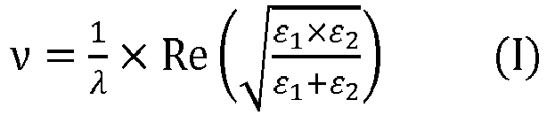
- The organic EL (electroluminescent) device according to claim 1, characterized in that, when λp represents the peak wavelength of the emission spectrum of the luminescent layer, S(λ) represents the intensity at the wavelength λ, λmin represents the minimum wavelength that satisfies S(λ) > S(λp)/100, λmax represents the maximum wavelength that satisfies S(λ) > S (λp)/100, k represents a real number larger than 0.8, spatial frequency ν1 represents the spatial frequency obtained by substituting λ1 obtained from Equation (II)


- The organic EL (electroluminescent) device according to claim 1, characterized in that the emission spectrum of the luminescent layer has a plurality of emission peak wavelengths λp1 ... λpn, and the surface plasmon absorption suppression area includes spatial frequencies νp1 ... νpn obtained by substituting λp1 ... λpn to λ of Equation (I).
- The organic EL (electroluminescent) device according to any one of claims 1 to 3, further comprising an uneven structure layer having a plurality of protrusions or recesses, characterized in that the uneven structure layer, the transparent electrode, the luminescent layer, and the cathode are stacked in this order on the first surface of the translucent substrate.
- The organic EL (electroluminescent) device according to claim 4, characterized in that the refractive index of the uneven structure layer is 1.7 or greater.
- The organic EL (electroluminescent) device according to claim 4, characterized in that the uneven structure layer comprises light scattering fine particles.
- The organic EL (electroluminescent) device according to claim 4, further comprising a prism structure, characterized in that the prism structure is provided between the translucent substrate and the uneven structure layer, and the refractive index of the prism structure is 1.7 or less.
- The organic EL (electroluminescent) device according to claim 4, characterized in that the plurality of protrusions or recesses of the uneven structure layer have an in-plane dimension of 1 mm or less.
Applications Claiming Priority (2)
| Application Number | Priority Date | Filing Date | Title |
|---|---|---|---|
| JP2015108994A JP6565338B2 (en) | 2015-05-28 | 2015-05-28 | Organic EL device |
| PCT/JP2016/002545 WO2016189868A1 (en) | 2015-05-28 | 2016-05-26 | Organic el element |
Publications (3)
| Publication Number | Publication Date |
|---|---|
| EP3307024A1 true EP3307024A1 (en) | 2018-04-11 |
| EP3307024A4 EP3307024A4 (en) | 2018-07-04 |
| EP3307024B1 EP3307024B1 (en) | 2022-06-29 |
Family
ID=57392662
Family Applications (1)
| Application Number | Title | Priority Date | Filing Date |
|---|---|---|---|
| EP16799581.0A Active EP3307024B1 (en) | 2015-05-28 | 2016-05-26 | Organic el element |
Country Status (6)
| Country | Link |
|---|---|
| US (1) | US10651415B2 (en) |
| EP (1) | EP3307024B1 (en) |
| JP (1) | JP6565338B2 (en) |
| KR (1) | KR102481193B1 (en) |
| CN (1) | CN107615885A (en) |
| WO (1) | WO2016189868A1 (en) |
Families Citing this family (5)
| Publication number | Priority date | Publication date | Assignee | Title |
|---|---|---|---|---|
| JP6622009B2 (en) * | 2015-06-11 | 2019-12-18 | 浜松ホトニクス株式会社 | Ultraviolet light generation target and method for producing the same |
| CN108476562B (en) * | 2015-12-10 | 2020-01-21 | 王子控股株式会社 | Substrate, optical element, mold, organic light-emitting element, organic thin-film solar cell, and method for manufacturing substrate |
| WO2019116754A1 (en) * | 2017-12-13 | 2019-06-20 | 富士フイルム株式会社 | Conductive member, touch panel, and display device |
| KR102640404B1 (en) * | 2018-10-18 | 2024-02-26 | 삼성디스플레이 주식회사 | Display device and manufacturing method for the same |
| CN114023909B (en) * | 2021-11-03 | 2024-03-05 | 昆山工研院新型平板显示技术中心有限公司 | Display panel and electronic equipment |
Family Cites Families (18)
| Publication number | Priority date | Publication date | Assignee | Title |
|---|---|---|---|---|
| JP2003036969A (en) * | 2000-10-25 | 2003-02-07 | Matsushita Electric Ind Co Ltd | Light emitting element, and display unit and illumination device using the same |
| US6670772B1 (en) * | 2002-06-27 | 2003-12-30 | Eastman Kodak Company | Organic light emitting diode display with surface plasmon outcoupling |
| GB0217900D0 (en) * | 2002-08-02 | 2002-09-11 | Qinetiq Ltd | Optoelectronic devices |
| JP2007207471A (en) * | 2006-01-31 | 2007-08-16 | Konica Minolta Holdings Inc | Surface emitter and display device |
| WO2008073601A2 (en) * | 2006-10-31 | 2008-06-19 | Trustees Of Boston University | Deterministic aperiodic patterned dielectric and plasmonic materials for localized electromagnetic field enhancement |
| KR101029299B1 (en) * | 2008-12-30 | 2011-04-18 | 서울대학교산학협력단 | Organic light emitting devices and fabrication method thereof |
| US8849072B2 (en) * | 2009-02-13 | 2014-09-30 | Physical Sciences, Inc. | Surface plasmon enhanced optical devices for integrated photonics |
| KR101521687B1 (en) * | 2009-07-16 | 2015-05-19 | 제이엑스 닛코닛세키에너지주식회사 | Diffraction grating, organic el element using same, and method for manufacturing said diffraction grating and organic el element |
| TWI602292B (en) | 2010-11-02 | 2017-10-11 | 王子控股股份有限公司 | Organic light emitting diode and method for producing the same, image display device and lighting device |
| DE102010062954A1 (en) * | 2010-12-13 | 2012-06-14 | Osram Opto Semiconductors Gmbh | Optoelectronic device and use of a copper complex in a charge generation layer sequence |
| CN103503571B (en) * | 2011-06-28 | 2016-03-30 | 松下知识产权经营株式会社 | Organic electroluminescent device |
| US9105878B2 (en) * | 2011-07-01 | 2015-08-11 | Oji Holdings Corporation | Organic light-emitting diode manufacturing method, organic light-emitting diode, image display device, illumination device, and substrate |
| EP2800456B1 (en) * | 2011-12-28 | 2019-03-06 | Oji Holdings Corporation | Organic light emitting diode, manufacturing method for organic light emitting diode |
| JP6118525B2 (en) * | 2012-09-03 | 2017-04-19 | 出光興産株式会社 | Organic electroluminescence device and electronic device |
| EP2975910A4 (en) * | 2013-03-13 | 2016-04-20 | Panasonic Corp | Organic electroluminescent element and lighting device using same |
| CN105340098B (en) * | 2013-06-27 | 2018-06-12 | 王子控股株式会社 | The manufacturing method of organic thin film solar cell and organic thin film solar cell |
| WO2015072070A1 (en) * | 2013-11-13 | 2015-05-21 | パナソニックIpマネジメント株式会社 | Organic electroluminescent element, illumination device, and display device |
| JP2016002545A (en) * | 2014-06-19 | 2016-01-12 | 株式会社フジコー | Air purifier |
-
2015
- 2015-05-28 JP JP2015108994A patent/JP6565338B2/en active Active
-
2016
- 2016-05-26 CN CN201680027144.3A patent/CN107615885A/en active Pending
- 2016-05-26 EP EP16799581.0A patent/EP3307024B1/en active Active
- 2016-05-26 WO PCT/JP2016/002545 patent/WO2016189868A1/en active Application Filing
- 2016-05-26 KR KR1020177037029A patent/KR102481193B1/en active IP Right Grant
-
2017
- 2017-11-27 US US15/822,286 patent/US10651415B2/en active Active
Also Published As
| Publication number | Publication date |
|---|---|
| JP6565338B2 (en) | 2019-08-28 |
| EP3307024A4 (en) | 2018-07-04 |
| KR20180013992A (en) | 2018-02-07 |
| US20180076410A1 (en) | 2018-03-15 |
| JP2016225086A (en) | 2016-12-28 |
| US10651415B2 (en) | 2020-05-12 |
| EP3307024B1 (en) | 2022-06-29 |
| CN107615885A (en) | 2018-01-19 |
| KR102481193B1 (en) | 2022-12-27 |
| WO2016189868A1 (en) | 2016-12-01 |
Similar Documents
| Publication | Publication Date | Title |
|---|---|---|
| US10651415B2 (en) | Organic EL (electroluminescent) device | |
| TWI540780B (en) | Organic electroluminescent element and lighting device | |
| US9774003B2 (en) | Organic electroluminescent element and electronic instrument | |
| KR101330461B1 (en) | Organic electroluminescent device, display device, and illumination device | |
| US8944616B2 (en) | Display device and image-information processing apparatus equipped with the same | |
| EP2986082A1 (en) | Light-emitting device | |
| JP5551200B2 (en) | ORGANIC ELECTROLUMINESCENT ELEMENT, LIGHTING DEVICE, AND METHOD FOR PRODUCING ORGANIC ELECTROLUMINESCENT ELEMENT | |
| KR101508399B1 (en) | Microlens for organic el devices, organic el device using the same, and their manufacturing process | |
| WO2010098480A1 (en) | Substrate and organic el device | |
| WO2013137184A1 (en) | Organic electroluminescence element | |
| KR20110021991A (en) | Led device structure to improve light output | |
| WO2014141623A1 (en) | Organic electroluminescent element and lighting device using same | |
| KR20080010458A (en) | Electroluminescence light source | |
| Riedel et al. | Polymer-based scattering layers for internal light extraction from organic light emitting diodes | |
| US20180351122A1 (en) | Substrate, optical element, mold, organic light-emitting element, organic thin-film solar cell, and method for producing substrate | |
| JP5566069B2 (en) | Organic electroluminescence display | |
| JP2011159394A (en) | Optical member, electroluminescent element, electroluminescent display device, electroluminescent lighting device | |
| Lee et al. | Enhanced light extraction from organic light-emitting diodes using a quasi-periodic nano-structure | |
| WO2017043274A1 (en) | Die, method for manufacturing organic light-emitting diode, and organic light-emitting diode | |
| JP2017162616A (en) | Organic el device | |
| WO2018014271A1 (en) | An organic light emitting display and a method for manufacturing an organic light emitting display | |
| JP6154580B2 (en) | ORGANIC ELECTROLUMINESCENT ELEMENT, METHOD FOR PRODUCING ORGANIC ELECTROLUMINESCENT ELEMENT, AND ELECTRONIC DEVICE |
Legal Events
| Date | Code | Title | Description |
|---|---|---|---|
| STAA | Information on the status of an ep patent application or granted ep patent |
Free format text: STATUS: THE INTERNATIONAL PUBLICATION HAS BEEN MADE |
|
| PUAI | Public reference made under article 153(3) epc to a published international application that has entered the european phase |
Free format text: ORIGINAL CODE: 0009012 |
|
| STAA | Information on the status of an ep patent application or granted ep patent |
Free format text: STATUS: REQUEST FOR EXAMINATION WAS MADE |
|
| 17P | Request for examination filed |
Effective date: 20171011 |
|
| AK | Designated contracting states |
Kind code of ref document: A1 Designated state(s): AL AT BE BG CH CY CZ DE DK EE ES FI FR GB GR HR HU IE IS IT LI LT LU LV MC MK MT NL NO PL PT RO RS SE SI SK SM TR |
|
| AX | Request for extension of the european patent |
Extension state: BA ME |
|
| A4 | Supplementary search report drawn up and despatched |
Effective date: 20180605 |
|
| RIC1 | Information provided on ipc code assigned before grant |
Ipc: H05B 33/26 20060101AFI20180529BHEP Ipc: H05B 33/02 20060101ALI20180529BHEP Ipc: G02B 5/02 20060101ALI20180529BHEP Ipc: H05B 33/28 20060101ALI20180529BHEP Ipc: H01L 51/50 20060101ALI20180529BHEP |
|
| DAV | Request for validation of the european patent (deleted) | ||
| DAX | Request for extension of the european patent (deleted) | ||
| STAA | Information on the status of an ep patent application or granted ep patent |
Free format text: STATUS: EXAMINATION IS IN PROGRESS |
|
| 17Q | First examination report despatched |
Effective date: 20200904 |
|
| STAA | Information on the status of an ep patent application or granted ep patent |
Free format text: STATUS: EXAMINATION IS IN PROGRESS |
|
| STAA | Information on the status of an ep patent application or granted ep patent |
Free format text: STATUS: EXAMINATION IS IN PROGRESS |
|
| REG | Reference to a national code |
Ref country code: DE Ref legal event code: R079 Ref document number: 602016073193 Country of ref document: DE Free format text: PREVIOUS MAIN CLASS: H05B0033260000 Ipc: H01L0051520000 |
|
| GRAP | Despatch of communication of intention to grant a patent |
Free format text: ORIGINAL CODE: EPIDOSNIGR1 |
|
| STAA | Information on the status of an ep patent application or granted ep patent |
Free format text: STATUS: GRANT OF PATENT IS INTENDED |
|
| RIC1 | Information provided on ipc code assigned before grant |
Ipc: H01L 51/52 20060101AFI20220314BHEP |
|
| INTG | Intention to grant announced |
Effective date: 20220411 |
|
| GRAS | Grant fee paid |
Free format text: ORIGINAL CODE: EPIDOSNIGR3 |
|
| GRAA | (expected) grant |
Free format text: ORIGINAL CODE: 0009210 |
|
| STAA | Information on the status of an ep patent application or granted ep patent |
Free format text: STATUS: THE PATENT HAS BEEN GRANTED |
|
| AK | Designated contracting states |
Kind code of ref document: B1 Designated state(s): AL AT BE BG CH CY CZ DE DK EE ES FI FR GB GR HR HU IE IS IT LI LT LU LV MC MK MT NL NO PL PT RO RS SE SI SK SM TR |
|
| REG | Reference to a national code |
Ref country code: CH Ref legal event code: EP |
|
| REG | Reference to a national code |
Ref country code: AT Ref legal event code: REF Ref document number: 1501902 Country of ref document: AT Kind code of ref document: T Effective date: 20220715 |
|
| REG | Reference to a national code |
Ref country code: IE Ref legal event code: FG4D |
|
| REG | Reference to a national code |
Ref country code: DE Ref legal event code: R096 Ref document number: 602016073193 Country of ref document: DE |
|
| REG | Reference to a national code |
Ref country code: LT Ref legal event code: MG9D |
|
| PG25 | Lapsed in a contracting state [announced via postgrant information from national office to epo] |
Ref country code: SE Free format text: LAPSE BECAUSE OF FAILURE TO SUBMIT A TRANSLATION OF THE DESCRIPTION OR TO PAY THE FEE WITHIN THE PRESCRIBED TIME-LIMIT Effective date: 20220629 Ref country code: NO Free format text: LAPSE BECAUSE OF FAILURE TO SUBMIT A TRANSLATION OF THE DESCRIPTION OR TO PAY THE FEE WITHIN THE PRESCRIBED TIME-LIMIT Effective date: 20220929 Ref country code: LT Free format text: LAPSE BECAUSE OF FAILURE TO SUBMIT A TRANSLATION OF THE DESCRIPTION OR TO PAY THE FEE WITHIN THE PRESCRIBED TIME-LIMIT Effective date: 20220629 Ref country code: HR Free format text: LAPSE BECAUSE OF FAILURE TO SUBMIT A TRANSLATION OF THE DESCRIPTION OR TO PAY THE FEE WITHIN THE PRESCRIBED TIME-LIMIT Effective date: 20220629 Ref country code: GR Free format text: LAPSE BECAUSE OF FAILURE TO SUBMIT A TRANSLATION OF THE DESCRIPTION OR TO PAY THE FEE WITHIN THE PRESCRIBED TIME-LIMIT Effective date: 20220930 Ref country code: FI Free format text: LAPSE BECAUSE OF FAILURE TO SUBMIT A TRANSLATION OF THE DESCRIPTION OR TO PAY THE FEE WITHIN THE PRESCRIBED TIME-LIMIT Effective date: 20220629 Ref country code: BG Free format text: LAPSE BECAUSE OF FAILURE TO SUBMIT A TRANSLATION OF THE DESCRIPTION OR TO PAY THE FEE WITHIN THE PRESCRIBED TIME-LIMIT Effective date: 20220929 |
|
| REG | Reference to a national code |
Ref country code: NL Ref legal event code: MP Effective date: 20220629 |
|
| REG | Reference to a national code |
Ref country code: AT Ref legal event code: MK05 Ref document number: 1501902 Country of ref document: AT Kind code of ref document: T Effective date: 20220629 |
|
| REG | Reference to a national code |
Ref country code: DE Ref legal event code: R079 Ref document number: 602016073193 Country of ref document: DE Free format text: PREVIOUS MAIN CLASS: H01L0051520000 Ipc: H10K0050800000 |
|
| PG25 | Lapsed in a contracting state [announced via postgrant information from national office to epo] |
Ref country code: RS Free format text: LAPSE BECAUSE OF FAILURE TO SUBMIT A TRANSLATION OF THE DESCRIPTION OR TO PAY THE FEE WITHIN THE PRESCRIBED TIME-LIMIT Effective date: 20220629 Ref country code: LV Free format text: LAPSE BECAUSE OF FAILURE TO SUBMIT A TRANSLATION OF THE DESCRIPTION OR TO PAY THE FEE WITHIN THE PRESCRIBED TIME-LIMIT Effective date: 20220629 |
|
| PG25 | Lapsed in a contracting state [announced via postgrant information from national office to epo] |
Ref country code: NL Free format text: LAPSE BECAUSE OF FAILURE TO SUBMIT A TRANSLATION OF THE DESCRIPTION OR TO PAY THE FEE WITHIN THE PRESCRIBED TIME-LIMIT Effective date: 20220629 |
|
| PG25 | Lapsed in a contracting state [announced via postgrant information from national office to epo] |
Ref country code: SM Free format text: LAPSE BECAUSE OF FAILURE TO SUBMIT A TRANSLATION OF THE DESCRIPTION OR TO PAY THE FEE WITHIN THE PRESCRIBED TIME-LIMIT Effective date: 20220629 Ref country code: SK Free format text: LAPSE BECAUSE OF FAILURE TO SUBMIT A TRANSLATION OF THE DESCRIPTION OR TO PAY THE FEE WITHIN THE PRESCRIBED TIME-LIMIT Effective date: 20220629 Ref country code: RO Free format text: LAPSE BECAUSE OF FAILURE TO SUBMIT A TRANSLATION OF THE DESCRIPTION OR TO PAY THE FEE WITHIN THE PRESCRIBED TIME-LIMIT Effective date: 20220629 Ref country code: PT Free format text: LAPSE BECAUSE OF FAILURE TO SUBMIT A TRANSLATION OF THE DESCRIPTION OR TO PAY THE FEE WITHIN THE PRESCRIBED TIME-LIMIT Effective date: 20221031 Ref country code: ES Free format text: LAPSE BECAUSE OF FAILURE TO SUBMIT A TRANSLATION OF THE DESCRIPTION OR TO PAY THE FEE WITHIN THE PRESCRIBED TIME-LIMIT Effective date: 20220629 Ref country code: EE Free format text: LAPSE BECAUSE OF FAILURE TO SUBMIT A TRANSLATION OF THE DESCRIPTION OR TO PAY THE FEE WITHIN THE PRESCRIBED TIME-LIMIT Effective date: 20220629 Ref country code: AT Free format text: LAPSE BECAUSE OF FAILURE TO SUBMIT A TRANSLATION OF THE DESCRIPTION OR TO PAY THE FEE WITHIN THE PRESCRIBED TIME-LIMIT Effective date: 20220629 |
|
| PG25 | Lapsed in a contracting state [announced via postgrant information from national office to epo] |
Ref country code: PL Free format text: LAPSE BECAUSE OF FAILURE TO SUBMIT A TRANSLATION OF THE DESCRIPTION OR TO PAY THE FEE WITHIN THE PRESCRIBED TIME-LIMIT Effective date: 20220629 Ref country code: IS Free format text: LAPSE BECAUSE OF FAILURE TO SUBMIT A TRANSLATION OF THE DESCRIPTION OR TO PAY THE FEE WITHIN THE PRESCRIBED TIME-LIMIT Effective date: 20221029 |
|
| REG | Reference to a national code |
Ref country code: DE Ref legal event code: R097 Ref document number: 602016073193 Country of ref document: DE |
|
| PG25 | Lapsed in a contracting state [announced via postgrant information from national office to epo] |
Ref country code: AL Free format text: LAPSE BECAUSE OF FAILURE TO SUBMIT A TRANSLATION OF THE DESCRIPTION OR TO PAY THE FEE WITHIN THE PRESCRIBED TIME-LIMIT Effective date: 20220629 |
|
| PG25 | Lapsed in a contracting state [announced via postgrant information from national office to epo] |
Ref country code: DK Free format text: LAPSE BECAUSE OF FAILURE TO SUBMIT A TRANSLATION OF THE DESCRIPTION OR TO PAY THE FEE WITHIN THE PRESCRIBED TIME-LIMIT Effective date: 20220629 Ref country code: CZ Free format text: LAPSE BECAUSE OF FAILURE TO SUBMIT A TRANSLATION OF THE DESCRIPTION OR TO PAY THE FEE WITHIN THE PRESCRIBED TIME-LIMIT Effective date: 20220629 |
|
| PLBE | No opposition filed within time limit |
Free format text: ORIGINAL CODE: 0009261 |
|
| STAA | Information on the status of an ep patent application or granted ep patent |
Free format text: STATUS: NO OPPOSITION FILED WITHIN TIME LIMIT |
|
| 26N | No opposition filed |
Effective date: 20230330 |
|
| P01 | Opt-out of the competence of the unified patent court (upc) registered |
Effective date: 20230530 |
|
| PGFP | Annual fee paid to national office [announced via postgrant information from national office to epo] |
Ref country code: DE Payment date: 20230331 Year of fee payment: 8 |
|
| PG25 | Lapsed in a contracting state [announced via postgrant information from national office to epo] |
Ref country code: SI Free format text: LAPSE BECAUSE OF FAILURE TO SUBMIT A TRANSLATION OF THE DESCRIPTION OR TO PAY THE FEE WITHIN THE PRESCRIBED TIME-LIMIT Effective date: 20220629 |
|
| REG | Reference to a national code |
Ref country code: CH Ref legal event code: PL |
|
| PG25 | Lapsed in a contracting state [announced via postgrant information from national office to epo] |
Ref country code: MC Free format text: LAPSE BECAUSE OF FAILURE TO SUBMIT A TRANSLATION OF THE DESCRIPTION OR TO PAY THE FEE WITHIN THE PRESCRIBED TIME-LIMIT Effective date: 20220629 |
|
| GBPC | Gb: european patent ceased through non-payment of renewal fee |
Effective date: 20230526 |
|
| REG | Reference to a national code |
Ref country code: BE Ref legal event code: MM Effective date: 20230531 |
|
| PG25 | Lapsed in a contracting state [announced via postgrant information from national office to epo] |
Ref country code: MC Free format text: LAPSE BECAUSE OF FAILURE TO SUBMIT A TRANSLATION OF THE DESCRIPTION OR TO PAY THE FEE WITHIN THE PRESCRIBED TIME-LIMIT Effective date: 20220629 Ref country code: LU Free format text: LAPSE BECAUSE OF NON-PAYMENT OF DUE FEES Effective date: 20230526 Ref country code: LI Free format text: LAPSE BECAUSE OF NON-PAYMENT OF DUE FEES Effective date: 20230531 Ref country code: IT Free format text: LAPSE BECAUSE OF FAILURE TO SUBMIT A TRANSLATION OF THE DESCRIPTION OR TO PAY THE FEE WITHIN THE PRESCRIBED TIME-LIMIT Effective date: 20220629 Ref country code: CH Free format text: LAPSE BECAUSE OF NON-PAYMENT OF DUE FEES Effective date: 20230531 |
|
| REG | Reference to a national code |
Ref country code: IE Ref legal event code: MM4A |
|
| PG25 | Lapsed in a contracting state [announced via postgrant information from national office to epo] |
Ref country code: IE Free format text: LAPSE BECAUSE OF NON-PAYMENT OF DUE FEES Effective date: 20230526 |