EP3306651A2 - Semiconductor device - Google Patents
Semiconductor device Download PDFInfo
- Publication number
- EP3306651A2 EP3306651A2 EP17195021.5A EP17195021A EP3306651A2 EP 3306651 A2 EP3306651 A2 EP 3306651A2 EP 17195021 A EP17195021 A EP 17195021A EP 3306651 A2 EP3306651 A2 EP 3306651A2
- Authority
- EP
- European Patent Office
- Prior art keywords
- rdl
- semiconductor device
- conductive
- molding compound
- electronic component
- Prior art date
- Legal status (The legal status is an assumption and is not a legal conclusion. Google has not performed a legal analysis and makes no representation as to the accuracy of the status listed.)
- Withdrawn
Links
Images





Classifications
-
- H—ELECTRICITY
- H10—SEMICONDUCTOR DEVICES; ELECTRIC SOLID-STATE DEVICES NOT OTHERWISE PROVIDED FOR
- H10W—GENERIC PACKAGES, INTERCONNECTIONS, CONNECTORS OR OTHER CONSTRUCTIONAL DETAILS OF DEVICES COVERED BY CLASS H10
- H10W74/00—Encapsulations, e.g. protective coatings
- H10W74/10—Encapsulations, e.g. protective coatings characterised by their shape or disposition
-
- H—ELECTRICITY
- H10—SEMICONDUCTOR DEVICES; ELECTRIC SOLID-STATE DEVICES NOT OTHERWISE PROVIDED FOR
- H10W—GENERIC PACKAGES, INTERCONNECTIONS, CONNECTORS OR OTHER CONSTRUCTIONAL DETAILS OF DEVICES COVERED BY CLASS H10
- H10W20/00—Interconnections in chips, wafers or substrates
- H10W20/20—Interconnections within wafers or substrates, e.g. through-silicon vias [TSV]
-
- H—ELECTRICITY
- H10—SEMICONDUCTOR DEVICES; ELECTRIC SOLID-STATE DEVICES NOT OTHERWISE PROVIDED FOR
- H10W—GENERIC PACKAGES, INTERCONNECTIONS, CONNECTORS OR OTHER CONSTRUCTIONAL DETAILS OF DEVICES COVERED BY CLASS H10
- H10W20/00—Interconnections in chips, wafers or substrates
- H10W20/40—Interconnections external to wafers or substrates, e.g. back-end-of-line [BEOL] metallisations or vias connecting to gate electrodes
- H10W20/482—Interconnections external to wafers or substrates, e.g. back-end-of-line [BEOL] metallisations or vias connecting to gate electrodes for individual devices provided for in groups H10D8/00 - H10D48/00, e.g. for power transistors
- H10W20/484—Interconnections having extended contours, e.g. pads having mesh shape or interconnections comprising connected parallel stripes
-
- H—ELECTRICITY
- H10—SEMICONDUCTOR DEVICES; ELECTRIC SOLID-STATE DEVICES NOT OTHERWISE PROVIDED FOR
- H10W—GENERIC PACKAGES, INTERCONNECTIONS, CONNECTORS OR OTHER CONSTRUCTIONAL DETAILS OF DEVICES COVERED BY CLASS H10
- H10W70/00—Package substrates; Interposers; Redistribution layers [RDL]
- H10W70/60—Insulating or insulated package substrates; Interposers; Redistribution layers
-
- H—ELECTRICITY
- H10—SEMICONDUCTOR DEVICES; ELECTRIC SOLID-STATE DEVICES NOT OTHERWISE PROVIDED FOR
- H10W—GENERIC PACKAGES, INTERCONNECTIONS, CONNECTORS OR OTHER CONSTRUCTIONAL DETAILS OF DEVICES COVERED BY CLASS H10
- H10W70/00—Package substrates; Interposers; Redistribution layers [RDL]
- H10W70/60—Insulating or insulated package substrates; Interposers; Redistribution layers
- H10W70/611—Insulating or insulated package substrates; Interposers; Redistribution layers for connecting multiple chips together
-
- H—ELECTRICITY
- H10—SEMICONDUCTOR DEVICES; ELECTRIC SOLID-STATE DEVICES NOT OTHERWISE PROVIDED FOR
- H10W—GENERIC PACKAGES, INTERCONNECTIONS, CONNECTORS OR OTHER CONSTRUCTIONAL DETAILS OF DEVICES COVERED BY CLASS H10
- H10W70/00—Package substrates; Interposers; Redistribution layers [RDL]
- H10W70/60—Insulating or insulated package substrates; Interposers; Redistribution layers
- H10W70/611—Insulating or insulated package substrates; Interposers; Redistribution layers for connecting multiple chips together
- H10W70/614—Insulating or insulated package substrates; Interposers; Redistribution layers for connecting multiple chips together the multiple chips being integrally enclosed
-
- H—ELECTRICITY
- H10—SEMICONDUCTOR DEVICES; ELECTRIC SOLID-STATE DEVICES NOT OTHERWISE PROVIDED FOR
- H10W—GENERIC PACKAGES, INTERCONNECTIONS, CONNECTORS OR OTHER CONSTRUCTIONAL DETAILS OF DEVICES COVERED BY CLASS H10
- H10W70/00—Package substrates; Interposers; Redistribution layers [RDL]
- H10W70/60—Insulating or insulated package substrates; Interposers; Redistribution layers
- H10W70/62—Insulating or insulated package substrates; Interposers; Redistribution layers characterised by their interconnections
- H10W70/63—Vias, e.g. via plugs
- H10W70/635—Through-vias
-
- H—ELECTRICITY
- H10—SEMICONDUCTOR DEVICES; ELECTRIC SOLID-STATE DEVICES NOT OTHERWISE PROVIDED FOR
- H10W—GENERIC PACKAGES, INTERCONNECTIONS, CONNECTORS OR OTHER CONSTRUCTIONAL DETAILS OF DEVICES COVERED BY CLASS H10
- H10W70/00—Package substrates; Interposers; Redistribution layers [RDL]
- H10W70/60—Insulating or insulated package substrates; Interposers; Redistribution layers
- H10W70/67—Insulating or insulated package substrates; Interposers; Redistribution layers characterised by their insulating layers or insulating parts
- H10W70/68—Shapes or dispositions thereof
- H10W70/685—Shapes or dispositions thereof comprising multiple insulating layers
-
- H—ELECTRICITY
- H10—SEMICONDUCTOR DEVICES; ELECTRIC SOLID-STATE DEVICES NOT OTHERWISE PROVIDED FOR
- H10W—GENERIC PACKAGES, INTERCONNECTIONS, CONNECTORS OR OTHER CONSTRUCTIONAL DETAILS OF DEVICES COVERED BY CLASS H10
- H10W90/00—Package configurations
-
- H—ELECTRICITY
- H10—SEMICONDUCTOR DEVICES; ELECTRIC SOLID-STATE DEVICES NOT OTHERWISE PROVIDED FOR
- H10W—GENERIC PACKAGES, INTERCONNECTIONS, CONNECTORS OR OTHER CONSTRUCTIONAL DETAILS OF DEVICES COVERED BY CLASS H10
- H10W70/00—Package substrates; Interposers; Redistribution layers [RDL]
- H10W70/60—Insulating or insulated package substrates; Interposers; Redistribution layers
- H10W70/67—Insulating or insulated package substrates; Interposers; Redistribution layers characterised by their insulating layers or insulating parts
- H10W70/69—Insulating materials thereof
- H10W70/695—Organic materials
-
- H—ELECTRICITY
- H10—SEMICONDUCTOR DEVICES; ELECTRIC SOLID-STATE DEVICES NOT OTHERWISE PROVIDED FOR
- H10W—GENERIC PACKAGES, INTERCONNECTIONS, CONNECTORS OR OTHER CONSTRUCTIONAL DETAILS OF DEVICES COVERED BY CLASS H10
- H10W70/00—Package substrates; Interposers; Redistribution layers [RDL]
- H10W70/60—Insulating or insulated package substrates; Interposers; Redistribution layers
- H10W70/67—Insulating or insulated package substrates; Interposers; Redistribution layers characterised by their insulating layers or insulating parts
- H10W70/69—Insulating materials thereof
- H10W70/698—Semiconductor materials that are electrically insulating, e.g. undoped silicon
-
- H—ELECTRICITY
- H10—SEMICONDUCTOR DEVICES; ELECTRIC SOLID-STATE DEVICES NOT OTHERWISE PROVIDED FOR
- H10W—GENERIC PACKAGES, INTERCONNECTIONS, CONNECTORS OR OTHER CONSTRUCTIONAL DETAILS OF DEVICES COVERED BY CLASS H10
- H10W72/00—Interconnections or connectors in packages
- H10W72/071—Connecting or disconnecting
- H10W72/072—Connecting or disconnecting of bump connectors
-
- H—ELECTRICITY
- H10—SEMICONDUCTOR DEVICES; ELECTRIC SOLID-STATE DEVICES NOT OTHERWISE PROVIDED FOR
- H10W—GENERIC PACKAGES, INTERCONNECTIONS, CONNECTORS OR OTHER CONSTRUCTIONAL DETAILS OF DEVICES COVERED BY CLASS H10
- H10W72/00—Interconnections or connectors in packages
- H10W72/071—Connecting or disconnecting
- H10W72/073—Connecting or disconnecting of die-attach connectors
-
- H—ELECTRICITY
- H10—SEMICONDUCTOR DEVICES; ELECTRIC SOLID-STATE DEVICES NOT OTHERWISE PROVIDED FOR
- H10W—GENERIC PACKAGES, INTERCONNECTIONS, CONNECTORS OR OTHER CONSTRUCTIONAL DETAILS OF DEVICES COVERED BY CLASS H10
- H10W72/00—Interconnections or connectors in packages
- H10W72/20—Bump connectors, e.g. solder bumps or copper pillars; Dummy bumps; Thermal bumps
- H10W72/241—Dispositions, e.g. layouts
-
- H—ELECTRICITY
- H10—SEMICONDUCTOR DEVICES; ELECTRIC SOLID-STATE DEVICES NOT OTHERWISE PROVIDED FOR
- H10W—GENERIC PACKAGES, INTERCONNECTIONS, CONNECTORS OR OTHER CONSTRUCTIONAL DETAILS OF DEVICES COVERED BY CLASS H10
- H10W72/00—Interconnections or connectors in packages
- H10W72/20—Bump connectors, e.g. solder bumps or copper pillars; Dummy bumps; Thermal bumps
- H10W72/251—Materials
- H10W72/252—Materials comprising solid metals or solid metalloids, e.g. PbSn, Ag or Cu
-
- H—ELECTRICITY
- H10—SEMICONDUCTOR DEVICES; ELECTRIC SOLID-STATE DEVICES NOT OTHERWISE PROVIDED FOR
- H10W—GENERIC PACKAGES, INTERCONNECTIONS, CONNECTORS OR OTHER CONSTRUCTIONAL DETAILS OF DEVICES COVERED BY CLASS H10
- H10W72/00—Interconnections or connectors in packages
- H10W72/90—Bond pads, in general
- H10W72/941—Dispositions of bond pads
- H10W72/9413—Dispositions of bond pads on encapsulations
-
- H—ELECTRICITY
- H10—SEMICONDUCTOR DEVICES; ELECTRIC SOLID-STATE DEVICES NOT OTHERWISE PROVIDED FOR
- H10W—GENERIC PACKAGES, INTERCONNECTIONS, CONNECTORS OR OTHER CONSTRUCTIONAL DETAILS OF DEVICES COVERED BY CLASS H10
- H10W74/00—Encapsulations, e.g. protective coatings
- H10W74/10—Encapsulations, e.g. protective coatings characterised by their shape or disposition
- H10W74/111—Encapsulations, e.g. protective coatings characterised by their shape or disposition the semiconductor body being completely enclosed
- H10W74/114—Encapsulations, e.g. protective coatings characterised by their shape or disposition the semiconductor body being completely enclosed by a substrate and the encapsulations
- H10W74/117—Encapsulations, e.g. protective coatings characterised by their shape or disposition the semiconductor body being completely enclosed by a substrate and the encapsulations the substrate having spherical bumps for external connection
-
- H—ELECTRICITY
- H10—SEMICONDUCTOR DEVICES; ELECTRIC SOLID-STATE DEVICES NOT OTHERWISE PROVIDED FOR
- H10W—GENERIC PACKAGES, INTERCONNECTIONS, CONNECTORS OR OTHER CONSTRUCTIONAL DETAILS OF DEVICES COVERED BY CLASS H10
- H10W74/00—Encapsulations, e.g. protective coatings
- H10W74/10—Encapsulations, e.g. protective coatings characterised by their shape or disposition
- H10W74/111—Encapsulations, e.g. protective coatings characterised by their shape or disposition the semiconductor body being completely enclosed
- H10W74/121—Encapsulations, e.g. protective coatings characterised by their shape or disposition the semiconductor body being completely enclosed by multiple encapsulations, e.g. by a thin protective coating and a thick encapsulation
-
- H—ELECTRICITY
- H10—SEMICONDUCTOR DEVICES; ELECTRIC SOLID-STATE DEVICES NOT OTHERWISE PROVIDED FOR
- H10W—GENERIC PACKAGES, INTERCONNECTIONS, CONNECTORS OR OTHER CONSTRUCTIONAL DETAILS OF DEVICES COVERED BY CLASS H10
- H10W74/00—Encapsulations, e.g. protective coatings
- H10W74/10—Encapsulations, e.g. protective coatings characterised by their shape or disposition
- H10W74/15—Encapsulations, e.g. protective coatings characterised by their shape or disposition on active surfaces of flip-chip devices, e.g. underfills
-
- H—ELECTRICITY
- H10—SEMICONDUCTOR DEVICES; ELECTRIC SOLID-STATE DEVICES NOT OTHERWISE PROVIDED FOR
- H10W—GENERIC PACKAGES, INTERCONNECTIONS, CONNECTORS OR OTHER CONSTRUCTIONAL DETAILS OF DEVICES COVERED BY CLASS H10
- H10W90/00—Package configurations
- H10W90/20—Configurations of stacked chips
- H10W90/297—Configurations of stacked chips characterised by the through-semiconductor vias [TSVs] in the stacked chips
-
- H—ELECTRICITY
- H10—SEMICONDUCTOR DEVICES; ELECTRIC SOLID-STATE DEVICES NOT OTHERWISE PROVIDED FOR
- H10W—GENERIC PACKAGES, INTERCONNECTIONS, CONNECTORS OR OTHER CONSTRUCTIONAL DETAILS OF DEVICES COVERED BY CLASS H10
- H10W90/00—Package configurations
- H10W90/701—Package configurations characterised by the relative positions of pads or connectors relative to package parts
- H10W90/721—Package configurations characterised by the relative positions of pads or connectors relative to package parts of bump connectors
- H10W90/722—Package configurations characterised by the relative positions of pads or connectors relative to package parts of bump connectors between stacked chips
-
- H—ELECTRICITY
- H10—SEMICONDUCTOR DEVICES; ELECTRIC SOLID-STATE DEVICES NOT OTHERWISE PROVIDED FOR
- H10W—GENERIC PACKAGES, INTERCONNECTIONS, CONNECTORS OR OTHER CONSTRUCTIONAL DETAILS OF DEVICES COVERED BY CLASS H10
- H10W90/00—Package configurations
- H10W90/701—Package configurations characterised by the relative positions of pads or connectors relative to package parts
- H10W90/721—Package configurations characterised by the relative positions of pads or connectors relative to package parts of bump connectors
- H10W90/724—Package configurations characterised by the relative positions of pads or connectors relative to package parts of bump connectors between a chip and a stacked insulating package substrate, interposer or RDL
-
- H—ELECTRICITY
- H10—SEMICONDUCTOR DEVICES; ELECTRIC SOLID-STATE DEVICES NOT OTHERWISE PROVIDED FOR
- H10W—GENERIC PACKAGES, INTERCONNECTIONS, CONNECTORS OR OTHER CONSTRUCTIONAL DETAILS OF DEVICES COVERED BY CLASS H10
- H10W90/00—Package configurations
- H10W90/701—Package configurations characterised by the relative positions of pads or connectors relative to package parts
- H10W90/731—Package configurations characterised by the relative positions of pads or connectors relative to package parts of die-attach connectors
- H10W90/734—Package configurations characterised by the relative positions of pads or connectors relative to package parts of die-attach connectors between a chip and a stacked insulating package substrate, interposer or RDL
Definitions
- the invention relates to a semiconductor device, and more particularly to a semiconductor device having redistribution layer (RDL) structure.
- RDL redistribution layer
- PoP Package-on-package
- PoP has a large size due to large volume of the molding compound, and the number of I/O contact is also less.
- a semiconductor device in one embodiment, includes a substrate, a body structure and an electronic component.
- the body structure is disposed above the substrate and includes a semiconductor die, a molding compound, a conductive component and a lower redistribution layer (RDL).
- the semiconductor die has an active surface.
- the molding compound encapsulates the semiconductor die and has a lower surface, an upper surface opposite to the lower surface and a through hole extending to the upper surface from the lower surface.
- the conductive component is formed within the through hole.
- the lower RDL is formed on the lower surface of the molding compound, the active surface of the semiconductor die and the conductive component exposed from the lower surface.
- the electronic component is disposed above the upper surface of the molding compound and electrically connected to the lower RDL through the conductive component.
- a semiconductor device in another embodiment, includes a molding substrate and an electronic component.
- the molding substrate includes a first molding compound, a first upper RDL, a lower RDL and a first conductive component.
- the first molding compound has an upper surface, a lower surface and a first through hole extending to the lower surface from the upper surface.
- the first upper RDL is formed on the upper surface of the first molding compound.
- the lower RDL is formed on the lower surface of the first molding compound.
- the first conductive component is formed within the first through hole and connects the lower RDL to the first upper RDL.
- the electronic component is disposed on the first upper RDL.
- a semiconductor device in another embodiment, includes a lower RDL, a body structure and a second molding compound.
- the body structure is disposed on the lower RDL and includes a silicon interposer, an electronic component and a first molding compound.
- the electronic component is disposed on the silicon interposer.
- the first molding compound encapsulates the electronic component and the silicon interposer.
- the second molding compound is formed on the lower RDL encapsulates the body structure.
- FIG. 1A illustrates a diagram of a semiconductor device 100 according to an embodiment of the invention
- FIG. 1B illustrates a top view of the semiconductor device 100 of FIG. 1A .
- the semiconductor device 100 includes a substrate 110, a body structure 120, at least one electronic component 130 and a plurality of conductive contacts 140.
- the substrate 110 is, for example, a multi-layered coreless substrate or a core-based substrate.
- the substrate 110 includes a plurality of upper pads 111 and a plurality of lower pads 112 electrically connected to the upper pads 111 through vias.
- the lower pads 112 are electrically connected to the conductive contacts 140, and the upper pads 111 are electrically connected to the body structure 120.
- the substrate 110 may be electrically connected to an exterior electronic device (not illustrated) through the conductive contacts 140.
- the substrate 110 may be formed of by semiconductor materials such as silicon, or organic materials such as bismaleimide triazine (BT), polyimide or Ajinomoto build-up film (ABF).
- BT bismaleimide triazine
- ABS Ajinomoto build-up film
- the body structure 120 is disposed above the substrate 110 and includes at least one semiconductor die 121, a molding compound 122, at least one conductive component 123, a lower redistribution layer (RDL) 124, a upper passivation layer 125 and at least one conductive contact 126.
- RDL redistribution layer
- the semiconductor die 121 may be formed by a silicon wafer, and thus the semiconductor die 121 is a silicon die.
- the semiconductor die 121 is a die not packaged, for example.
- the semiconductor die 121 is, for example, a SOC (System on Chip) and has an active surface 121 a facing the RDL 124.
- the molding compound 122 may be made of different material from that of the substrate 110.
- the molding compound 122 encapsulates the semiconductor die 121 and has a lower surface 122b, an upper surface 122u opposite to the lower surface 122b and at least one through hole 122h extending to the upper surface 122u from the lower surface 122b.
- the conductive components 123 are formed by filling the through holes 122h with conductive material, such as metal.
- the molding compound 122 may be formed of an epoxy, a resin, a moldable polymer, or the like.
- the molding compound 122 may be applied while substantially liquid, and then may be cured through a chemical reaction, such as in an epoxy or resin.
- the molding compound 122 may be an ultraviolet (UV) or thermally cured polymer applied as a gel or malleable solid capable of being disposed around the semiconductor die, and then may be cured through a UV or thermal curing process.
- the molding compound may be cured with a mold (not shown).
- the lower RDL 124 is formed on the lower surface 122b of the molding compound 122, the active surface 121a of the semiconductor die 121 and the conductive components 123 exposed from the lower surface 122b.
- the lower RDL 124 extends beyond a lateral surface 121s of the semiconductor die 121 to form a fan-out structure.
- the lower RDL 124 includes a lower dielectric layer 1241, a lower conductive layer 1242, a lower passivation layer 1243 and at least one conductive contact 1244.
- the lower RDL 124 may include more layer structures, such as dielectric layer, conductive layer, etc.
- the lower dielectric layer 1241 is formed on the lower surface 122b and has at least one lower opening 1241h exposing the conductive component 123.
- the lower conductive layer 1242 is formed on the lower dielectric layer 1241 and laterally extends beyond the lateral surface 121s of the semiconductor die 121 to be electrically connected to the conductive components 123 through the lower opening 1241h.
- the lower passivation layer 1243 covers the lower conductive layer 1242 and has at least one lower opening 1243h exposing the lower conductive layer 1242, and each conductive contact 1244 is formed within the corresponding lower opening 1243h for electrically connected to the lower conductive layer 1242 through the corresponding lower opening 1243h.
- the conductive contact 1244 may be solder ball, conductive pillar, conductive bump, etc. Due to the design of the RDL, the conductive contact 1244 may be micro pillar or micro pad, and accordingly I/O contacts of the body structure 120 may be increased, and the size of the semiconductor device 100 can be more compact.
- the upper passivation layer 125 covers the upper surface 122u of the molding compound 122 and has at least one upper opening 125h exposing the corresponding conductive component 123.
- Each conductive contact 126 is formed within the corresponding upper opening 125h to be electrically connected to the corresponding conductive component 123.
- Each electronic component 130 has at least one conductive contact 131, and the electronic component 130 is disposed on the upper conductive pad 126 by the conductive contact 131 through a solder 132.
- the conductive contact 131 is, for example, solder ball, conductive pillar, conductive bump, etc. Since the upper conductive pad 126 projects from an upper surface 125u of the upper passivation layer 125 and provides a large area, it can increase the reliability of the connecting between the upper conductive pad 126 and the conductive contact 131.
- the electronic components 130 are disposed above the upper surface 122u of the molding compound 122 and electrically connected to the substrate 110 through the conductive components 123 and the lower RDL 124.
- the electronic component 130 is, for example, High Bandwidth Memory (HBM) or other suitable memory components.
- the electronic component 130 may have the structure similar or the same as that of the semiconductor die 121.
- the electronic components 130 do not overlap the semiconductor die 121 in a stack direction of the electronic component 130 and the semiconductor die 121 (that is, up and down).
- the number of the electronic components 130 may be plural or one.
- the electronic components 130 may be disposed on any positions of the upper surface 122u of the molding compound 122.
- FIG. 2 illustrates a diagram of a semiconductor device 200 according to another embodiment of the invention.
- the semiconductor device 200 includes the substrate 110, the body structure 120, at least one an electronic component 130, at least one conductive contact 140, a first underfill 150 and a plurality of second underfills 160.
- the first underfill 150 is formed between the body structure 120 and the substrate 110 to encapsulate the lower RDL 124.
- the second underfill 160 is formed between the electronic component 130 and the body structure 120 to encapsulate the conductive contacts 131 and upper conductive pads 126.
- FIG. 3A illustrates a diagram of a semiconductor device 300 according to another embodiment of the invention
- FIG. 3B illustrates a top view of the semiconductor device 300 of FIG. 3A .
- the semiconductor device 300 includes the substrate 110, the body structure 220, at least one electronic component 130, at least one conductive contact 140, the first underfill 150 and the second underfills 160.
- the body structure 220 is disposed above the substrate 110 and includes the semiconductor die 121, the molding compound 122, at least one conductive component 123, the lower RDL 124 and an upper RDL 227.
- the upper RDL 227 is formed on the upper surface 122u of the molding compound 122 and the conductive components 123 exposed from the upper surface 122u. Due to the upper RDL 227 being formed over the semiconductor die 121, the electronic component 130 can be connected to the upper RDL 227 right above the semiconductor die 121 by way of the electronic component 130 overlapping the semiconductor die 121 up and down.
- the electronic components 130 overlap the semiconductor die 121 up and down.
- one or some of the electronic components 130 may not overlap the semiconductor die 121 while another or the others of the electronic components 130 may overlap the semiconductor die 121 up and down.
- the upper RDL 227 can provide fine pitch between the adjacent two upper conductive pads 126, and accordingly a pitch between adjacent two conductive contacts 131 also can be designed as fine pitch. As a result, it provides more input/output contacts in the electronic component 130.
- the upper RDL 227 includes an upper dielectric layer 2271, an upper conductive layer 2272, an upper passivation layer 125 and at least one upper conductive pad 126.
- the upper dielectric layer 2271 is formed on the upper surface 122u and has at least one upper opening 2271 h exposing the corresponding conductive component 123.
- the upper conductive layer 2272 is formed on the upper dielectric layer 2271 to be electrically connected to the conductive component 123 through the corresponding upper opening 2271h.
- the upper passivation layer 125 covers the upper conductive layer 2272 and has at least one upper opening 125h exposing the upper conductive layer 2272.
- Each conductive contact 126 is formed within the corresponding upper opening 125h to be electrically connected to the upper conductive layer 2272.
- the upper RDL 227 may include more layer structures, such as dielectric layer, conductive layer, etc.
- FIG. 4A illustrates a diagram of a semiconductor device 400 according to another embodiment of the invention
- FIG. 4B illustrates a top view of the semiconductor device 400 of FIG. 4A .
- the semiconductor device 400 includes the substrate 110, the silicon interposer 420, at least one an electronic component 130, a plurality of conductive contacts 140, the first underfill 150 and the second underfills 160.
- the silicon interposer 420 is electrically connected to the substrate 110 through at least one conductive contact 425 disposed between a lower surface 420b of the silicon interposer 420 and the substrate 110.
- the conductive contact 425 may be solder ball, conductive pillar, conductive bump, etc.
- the silicon interposer 420 is disposed above the substrate 110 and includes a silicon substrate 421, at least one conductive component 422 and an upper RDL 423.
- the silicon substrate 421 has a lower surface 421b, an upper surface 421u opposite to the lower surface 421b and at least one through hole 421h extending to the lower surface 421b from the upper surface 421u.
- Each conductive component 422 is formed within the corresponding through hole 421h.
- the through hole 421h is through-silicon via (TSV), for example.
- the upper RDL 423 is formed on the upper surface 421u of the silicon substrate 421 and the conductive components 422 exposed from the upper surface 421u.
- the electronic components 130 are disposed above the upper RDL 423 and electrically connected to the upper RDL 423.
- the electronic components 130 may include at least one SoC 130', at least one HBM 130"or other suitable electronic component.
- the upper RDL 423 includes an upper dielectric layer 4231, an upper conductive layer 4232, an upper passivation layer 4233 and at least one upper conductive pad 4234.
- the upper dielectric layer 4231 is formed on the upper surface 421u and has at least one upper opening 4231h exposing the corresponding conductive component 422.
- the upper conductive layer 4232 is formed on the upper dielectric layer 4231 to be electrically connected to the conductive components 422 through the corresponding upper openings 4231h.
- the passivation layer 4233 covers the conductive layer 4232 and has at least one upper opening 4233h exposing the upper conductive layer 4232.
- Each conductive contact 4234 is formed within the corresponding upper opening 4233h to be electrically connected to the upper conductive layer 4232. Due to the design of the upper RDL 423, the conductive contact 131 of the electronic component 130 may be micro pillar or micro pad, and accordingly it provides more input/output contacts in the electronic component 130.
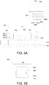
- FIG. 5A illustrates a diagram of a semiconductor device 500 according to another embodiment of the invention
- FIG. 5B illustrates a top view of the semiconductor device 500 of FIG. 5A .
- the semiconductor device 500 includes the substrate 110, the silicon interposer 420, at least one an electronic component 130, a plurality of conductive contacts 140, the first underfill 150, the second underfills 160 and a surrounding component 550.
- the surrounding component 550 is formed on and surrounds an outer lateral surface 420s of the silicon interposer 420.
- the outer lateral surface 420s is defined by an outer lateral surface 423s of the upper RDL 423 and an outer lateral surface 421s of the silicon substrate 421, wherein the outer lateral surface 423s is aligned with the outer lateral surface 421s.
- the silicon substrate 421 of the semiconductor device 500 has a shorter length L1 than the length L1 of the silicon substrate 421 of the semiconductor device 400, and accordingly it can reduce the cost of the silicon substrate 421 of semiconductor device 500.
- the surrounding component 550 may be made of molding compound material as described above. The molding compound material is cheaper than the silicon wafer, and accordingly it can reduce the cost of the silicon substrate 421 of semiconductor device 500.
- the electronic component 130 has an outer lateral surface 130s located between an outer lateral surface 550s of the surrounding component 550 and the outer lateral surface 420s of the silicon interposer 420. In other words, the electronic component 130 overlaps the surrounding component 550 in the stack direction.
- FIG. 6 illustrates a diagram of a semiconductor device 600 according to another embodiment of the invention.
- the semiconductor device 600 includes a lower RDL 610, a body structure 620, a second molding compound 630 and at least one conductive contact 140.
- the lower RDL 610 is, for example, similar to or the same as the lower RDL 124 described above.
- the lower RDL 610 is directly connected to a lower surface 421b of the silicon substrate 421, a lower surface 621b of the first molding compound 621 and a lower surface 630b of the second molding compound 630.
- the lower RDL 610 is directly electrically connected to the body structure 620 without any conductive contact (for example, solder ball, conductive pillar, conductive bump, etc.) formed between the body structure 620 and the lower RDL 610.
- the body structure 620 is, for example, a 2.5D structure.
- the body structure 620 includes at least one electronic component 130, at least one second underfill 150, the silicon interposer 420 and a first molding compound 621.
- the silicon interposer 420 is disposed on the lower RDL 610 and includes the silicon substrate 421, at least one conductive component 422 and the upper RDL 423, as described above.
- the first molding compound 621 encapsulates the silicon interposer 420, the electronic components 130 and the second underfills 150.
- the second molding compound 630 is formed on an upper surface 610u of the lower RDL 610 and encapsulates the body structure 620.
- the lower RDL 610 and the body structure 620 are combined after the body structure 620 is encapsulated by the second molding compound 630, and such method calls "RDL last" or "Die first".
- FIG. 7 illustrates a diagram of a semiconductor device 700 according to another embodiment of the invention.
- the semiconductor device 700 includes a lower RDL 710, the body structure 620, a second molding compound 630 and at least one conductive contact 140.
- the body structure 620 may be omitted.
- the second molding compound 630 is formed between the body structure 620 and the lower RDL 710.
- the lower RDL 710 includes a first lower passivation layer 711, a lower conductive layer 712, a second lower passivation layer 713 and at least one conductive contact 714.
- the first lower passivation layer 711 is formed below the lower conductive layer 712 and has at least one lower opening 711h to expose a lower surface of the lower conductive layer 712.
- the second lower passivation layer 713 is formed above the lower conductive layer 712 and has at least one lower opening 713h to expose an upper surface of the lower conductive layer 712.
- Each conductive contact 714 is formed within the corresponding lower opening 713h, for electrically connected to the corresponding conductive component 422.
- the lower RDL 710 and the body structure 620 are combined after the lower RDL 710 is formed, and such method calls "RDL first" or "Die last".
- FIG. 8 illustrates a diagram of a semiconductor device 800 according to another embodiment of the invention.
- the semiconductor device 800 includes the substrate 110, a body structure 820 and at least one conductive contact 140.
- the body structure 820 is disposed on the substrate 110 and includes the lower RDL 124, at least one semiconductor die 121 and a molding compound 821.
- the semiconductor dies 121 are disposed on the lower RDL 124.
- the conductive contacts 1244 of the lower RDL 124 are disposed between the substrate 110 and the lower passivation layer 1243 of the lower RDL 124 for being electrically connecting the lower conductive layer 1242 of the lower RDL 124 to the substrate 110.
- the conductive contacts 1244 is, for example, solder ball.
- the lower RDL 124 is formed below the semiconductor dies 121 and the molding compound 821, and directly connected to the semiconductor dies 121 without any conductive contact (for example, solder ball, conductive pillar, conductive bump, etc.) formed between the semiconductor dies 121 and the lower RDL 124.
- any conductive contact for example, solder ball, conductive pillar, conductive bump, etc.
- the lower RDL 124 and the semiconductor dies 121 are combined after the semiconductor dies 121 are encapsulated by the molding compound 821, and such method calls "RDL last" or "Die first".
- FIG. 9 illustrates a diagram of a semiconductor device 900 according to another embodiment of the invention.
- the semiconductor device 900 includes the substrate 110, at least one conductive contact 140 and a body structure 920.
- the body structure 920 is disposed on the substrate 110 and includes a lower RDL 924, at least one semiconductor die 121 and a molding compound 821.
- the semiconductor dies 121 are disposed on the lower RDL 924.
- the lower RDL 924 includes a first lower passivation layer 9241, a lower conductive layer 9242, a second lower passivation layer 9243, at least one conductive pad 9244 and at least one conductive contact 1244.
- the lower conductive layer 9242 is formed between the first lower passivation layer 9241 and the second lower passivation layer 9243.
- the first lower passivation layer 9241 has at least one lower opening 9241h to expose a lower surface of the lower conductive layer 9242
- the second lower passivation layer 9243 has at least one opening 9243h to expose an upper surface of the lower conductive layer 9242.
- Each conductive pad 9244 is formed within the corresponding lower opening 9243h
- each conductive contact 822 is formed within the corresponding opening 9241h.
- the lower RDL 924 and the semiconductor dies 121 are combined after the lower RDL 924 is formed, and such method calls "RDL first" or "Die last".
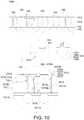
- FIG. 10 illustrates a diagram of a semiconductor device 1000 according to another embodiment of the invention.
- the semiconductor device 1000 includes the molding substrate 1010, at least one semiconductor diel 21, at least one conductive contact 140 and at least one second underfill 160.
- the molding substrate 1010 includes a first molding compound 1011, at least one first conductive component 1012, a first upper RDL 1013, a semiconductor die 1014, the lower RDL 124 and the second underfills 160.
- the first upper RDL 1013 has the structures similar to or the same as that of the upper RDL 423 as described above.
- the first molding compound 1011 has an upper surface 1011u, a lower surface 1011b and at least one first through hole 1011h extending to the lower surface 1011b from the upper surface 1011u.
- Each first conductive component 1012 is formed within the corresponding first through hole 1011h and connects the lower RDL 124 to the first upper RDL 1013.
- the first upper RDL 1013 is formed on the upper surface 1011u.
- the lower RDL 124 is formed on the lower surface 1011b.
- the semiconductor dies 121 are disposed on the first upper RDL 1013.
- the first upper RDL 1013 includes the upper dielectric layer 4231, the upper conductive layer 4232, the upper passivation layer 4233 and at least one conductive pad 4234.
- the upper dielectric layer 4231 has at least one upper opening 4231 h exposing the first through holes 1011h and a second upper RDL 1015 of the semiconductor die 1014.
- the upper conductive layer 4232 is formed on the first conductive components 1012 and the second upper RDL 1015 of the semiconductor die 1014 through the upper openings 4231h.
- the semiconductor die 1014 may be formed by a silicon wafer, and thus the semiconductor die 1014 is a silicon die.
- the semiconductor die 1014 is embedded in the first molding compound 1011 of the molding substrate 1010 and includes a second upper RDL 1015, a silicon substrate 1016, at least one second conductive component 1017.
- the silicon substrate 1016 has an upper surface 1016u and a lower surface 1016u opposite to the upper surface 1016u.
- the semiconductor die 1014 has a second through hole 1014h extending to the lower surface 1016b from the upper surface 1016u. Each second conductive component 1017 is formed within the corresponding second through hole 1014h.
- the first molding compound 1011 has a blind hole 1011a extending to the second conductive component 1017 from the lower surface 1011b of the first molding compound 1011.
- the molding substrate 1010 further includes at least third conductive component 1018 formed within the blind hole 1011a to electrically connect the corresponding second conductive component 1017 to the lower RDL 124.
- the semiconductor die 1014 can provide the molding substrate 1010 with more I/O density, trace density and various routing designs. In another embodiment, the semiconductor die 1014 may be omitted.
- FIG. 11 illustrates a diagram of a semiconductor device 1100 according to another embodiment of the invention.
- the semiconductor device 1100 includes the molding substrate 1010, a second molding compound 1020, at least one semiconductor die 121, at least one conductive contact 140 and at least one second underfill 160.
- the second molding compound 1020 formed on the first upper RDL 1013 encapsulates the semiconductor dies 121 and the second underfills 160.
Landscapes
- Structures Or Materials For Encapsulating Or Coating Semiconductor Devices Or Solid State Devices (AREA)
- Internal Circuitry In Semiconductor Integrated Circuit Devices (AREA)
Abstract
Description
- The invention relates to a semiconductor device, and more particularly to a semiconductor device having redistribution layer (RDL) structure.
- In the electronics industry, high integration and multiple functions with high performance become essential for new products. And meanwhile, high integration may cause higher manufacturing cost, since the manufacturing cost is in proportional to its size. Therefore, demanding on miniaturization of integrated circuit (IC) packages has become more and more critical.
- Package-on-package (PoP) is now the fastest growing semiconductor package technology since it is a cost-effective solution to high-density system integration in a single package. In a PoP structure, various packages are integrated in a single semiconductor package to reduce the size.
- However, PoP has a large size due to large volume of the molding compound, and the number of I/O contact is also less.
- In one embodiment of the invention, a semiconductor device is provided. The semiconductor device includes a substrate, a body structure and an electronic component. The body structure is disposed above the substrate and includes a semiconductor die, a molding compound, a conductive component and a lower redistribution layer (RDL). The semiconductor die has an active surface. The molding compound encapsulates the semiconductor die and has a lower surface, an upper surface opposite to the lower surface and a through hole extending to the upper surface from the lower surface. The conductive component is formed within the through hole. The lower RDL is formed on the lower surface of the molding compound, the active surface of the semiconductor die and the conductive component exposed from the lower surface. The electronic component is disposed above the upper surface of the molding compound and electrically connected to the lower RDL through the conductive component.
- In another embodiment of the invention, a semiconductor device is provided. The semiconductor device includes a molding substrate and an electronic component. The molding substrate includes a first molding compound, a first upper RDL, a lower RDL and a first conductive component. The first molding compound has an upper surface, a lower surface and a first through hole extending to the lower surface from the upper surface. The first upper RDL is formed on the upper surface of the first molding compound. The lower RDL is formed on the lower surface of the first molding compound. The first conductive component is formed within the first through hole and connects the lower RDL to the first upper RDL. The electronic component is disposed on the first upper RDL.
- In another embodiment of the invention, a semiconductor device is provided. The semiconductor device includes a lower RDL, a body structure and a second molding compound. The body structure is disposed on the lower RDL and includes a silicon interposer, an electronic component and a first molding compound. The electronic component is disposed on the silicon interposer. The first molding compound encapsulates the electronic component and the silicon interposer. The second molding compound is formed on the lower RDL encapsulates the body structure.
- Numerous objects, features and advantages of the invention will be readily apparent upon a reading of the following detailed description of embodiments of the invention when taken in conjunction with the accompanying drawings. However, the drawings employed herein are for the purpose of descriptions and should not be regarded as limiting.
- The above objects and advantages of the invention will become more readily apparent to those ordinarily skilled in the art after reviewing the following detailed description and accompanying drawings, in which:
-
FIG. 1A illustrates a diagram of a semiconductor device according to an embodiment of the invention; -
FIG. 1B illustrates a top view of the semiconductor device ofFIG. 1 A; -
FIG. 2 illustrates a diagram of a semiconductor device according to another embodiment of the invention; -
FIG. 3A illustrates a diagram of a semiconductor device according to another embodiment of the invention; -
FIG. 3B illustrates a top view of the semiconductor device ofFIG. 3A ; -
FIG. 4A illustrates a diagram of a semiconductor device according to another embodiment of the invention; -
FIG. 4B illustrates a top view of the semiconductor device ofFIG. 4A ; -
FIG. 5A illustrates a diagram of a semiconductor device according to another embodiment of the invention; -
FIG. 5B illustrates a top view of the semiconductor device ofFIG. 5A ; -
FIG. 6 illustrates a diagram of a semiconductor device according to another embodiment of the invention; -
FIG. 7 illustrates a diagram of a semiconductor device according to another embodiment of the invention; -
FIG. 8 illustrates a diagram of a semiconductor device according to another embodiment of the invention; -
FIG. 9 illustrates a diagram of a semiconductor device according to another embodiment of the invention; -
FIG. 10 illustrates a diagram of a semiconductor device according to another embodiment of the invention; and -
FIG. 11 illustrates a diagram of a semiconductor device according to another embodiment of the invention. -
FIG. 1A illustrates a diagram of asemiconductor device 100 according to an embodiment of the invention, andFIG. 1B illustrates a top view of thesemiconductor device 100 ofFIG. 1A . - The
semiconductor device 100 includes asubstrate 110, abody structure 120, at least oneelectronic component 130 and a plurality ofconductive contacts 140. - The
substrate 110 is, for example, a multi-layered coreless substrate or a core-based substrate. Thesubstrate 110 includes a plurality ofupper pads 111 and a plurality oflower pads 112 electrically connected to theupper pads 111 through vias. Thelower pads 112 are electrically connected to theconductive contacts 140, and theupper pads 111 are electrically connected to thebody structure 120. Thesubstrate 110 may be electrically connected to an exterior electronic device (not illustrated) through theconductive contacts 140. In addition, thesubstrate 110 may be formed of by semiconductor materials such as silicon, or organic materials such as bismaleimide triazine (BT), polyimide or Ajinomoto build-up film (ABF). - The
body structure 120 is disposed above thesubstrate 110 and includes at least one semiconductor die 121, amolding compound 122, at least oneconductive component 123, a lower redistribution layer (RDL) 124, aupper passivation layer 125 and at least oneconductive contact 126. - The semiconductor die 121 may be formed by a silicon wafer, and thus the semiconductor die 121 is a silicon die. The semiconductor die 121 is a die not packaged, for example. In an embodiment, the semiconductor die 121 is, for example, a SOC (System on Chip) and has an
active surface 121 a facing theRDL 124. - The
molding compound 122 may be made of different material from that of thesubstrate 110. Themolding compound 122 encapsulates the semiconductor die 121 and has alower surface 122b, anupper surface 122u opposite to thelower surface 122b and at least one throughhole 122h extending to theupper surface 122u from thelower surface 122b. Theconductive components 123 are formed by filling the throughholes 122h with conductive material, such as metal. - The
molding compound 122 may be formed of an epoxy, a resin, a moldable polymer, or the like. Themolding compound 122 may be applied while substantially liquid, and then may be cured through a chemical reaction, such as in an epoxy or resin. In some other embodiments, themolding compound 122 may be an ultraviolet (UV) or thermally cured polymer applied as a gel or malleable solid capable of being disposed around the semiconductor die, and then may be cured through a UV or thermal curing process. The molding compound may be cured with a mold (not shown). - The
lower RDL 124 is formed on thelower surface 122b of themolding compound 122, theactive surface 121a of the semiconductor die 121 and theconductive components 123 exposed from thelower surface 122b. - The
lower RDL 124 extends beyond alateral surface 121s of the semiconductor die 121 to form a fan-out structure. Thelower RDL 124 includes alower dielectric layer 1241, a lowerconductive layer 1242, alower passivation layer 1243 and at least oneconductive contact 1244. In another embodiment, thelower RDL 124 may include more layer structures, such as dielectric layer, conductive layer, etc. - The
lower dielectric layer 1241 is formed on thelower surface 122b and has at least onelower opening 1241h exposing theconductive component 123. The lowerconductive layer 1242 is formed on thelower dielectric layer 1241 and laterally extends beyond thelateral surface 121s of the semiconductor die 121 to be electrically connected to theconductive components 123 through thelower opening 1241h. Thelower passivation layer 1243 covers the lowerconductive layer 1242 and has at least onelower opening 1243h exposing the lowerconductive layer 1242, and eachconductive contact 1244 is formed within the correspondinglower opening 1243h for electrically connected to the lowerconductive layer 1242 through the correspondinglower opening 1243h. In addition, theconductive contact 1244 may be solder ball, conductive pillar, conductive bump, etc. Due to the design of the RDL, theconductive contact 1244 may be micro pillar or micro pad, and accordingly I/O contacts of thebody structure 120 may be increased, and the size of thesemiconductor device 100 can be more compact. - The
upper passivation layer 125 covers theupper surface 122u of themolding compound 122 and has at least oneupper opening 125h exposing the correspondingconductive component 123. Eachconductive contact 126 is formed within the correspondingupper opening 125h to be electrically connected to the correspondingconductive component 123. - Each
electronic component 130 has at least oneconductive contact 131, and theelectronic component 130 is disposed on the upperconductive pad 126 by theconductive contact 131 through asolder 132. Theconductive contact 131 is, for example, solder ball, conductive pillar, conductive bump, etc. Since the upperconductive pad 126 projects from anupper surface 125u of theupper passivation layer 125 and provides a large area, it can increase the reliability of the connecting between the upperconductive pad 126 and theconductive contact 131. - The
electronic components 130 are disposed above theupper surface 122u of themolding compound 122 and electrically connected to thesubstrate 110 through theconductive components 123 and thelower RDL 124. In one embodiment, theelectronic component 130 is, for example, High Bandwidth Memory (HBM) or other suitable memory components. In another embodiment, theelectronic component 130 may have the structure similar or the same as that of the semiconductor die 121. - As illustrated in
FIGS. 1A and 1B , theelectronic components 130 do not overlap the semiconductor die 121 in a stack direction of theelectronic component 130 and the semiconductor die 121 (that is, up and down). The number of theelectronic components 130 may be plural or one. As long as theelectronic components 130 can be electrically connected to theconductive components 123, theelectronic components 130 may be disposed on any positions of theupper surface 122u of themolding compound 122. -
FIG. 2 illustrates a diagram of asemiconductor device 200 according to another embodiment of the invention. - The
semiconductor device 200 includes thesubstrate 110, thebody structure 120, at least one anelectronic component 130, at least oneconductive contact 140, afirst underfill 150 and a plurality ofsecond underfills 160. - The
first underfill 150 is formed between thebody structure 120 and thesubstrate 110 to encapsulate thelower RDL 124. Thesecond underfill 160 is formed between theelectronic component 130 and thebody structure 120 to encapsulate theconductive contacts 131 and upperconductive pads 126. -
FIG. 3A illustrates a diagram of asemiconductor device 300 according to another embodiment of the invention, andFIG. 3B illustrates a top view of thesemiconductor device 300 ofFIG. 3A . - The
semiconductor device 300 includes thesubstrate 110, thebody structure 220, at least oneelectronic component 130, at least oneconductive contact 140, thefirst underfill 150 and thesecond underfills 160. - In the present embodiment, the
body structure 220 is disposed above thesubstrate 110 and includes the semiconductor die 121, themolding compound 122, at least oneconductive component 123, thelower RDL 124 and anupper RDL 227. - The
upper RDL 227 is formed on theupper surface 122u of themolding compound 122 and theconductive components 123 exposed from theupper surface 122u. Due to theupper RDL 227 being formed over the semiconductor die 121, theelectronic component 130 can be connected to theupper RDL 227 right above the semiconductor die 121 by way of theelectronic component 130 overlapping the semiconductor die 121 up and down. - As illustrated in
FIG. 3B , theelectronic components 130 overlap the semiconductor die 121 up and down. In another embodiment, one or some of theelectronic components 130 may not overlap the semiconductor die 121 while another or the others of theelectronic components 130 may overlap the semiconductor die 121 up and down. - The
upper RDL 227 can provide fine pitch between the adjacent two upperconductive pads 126, and accordingly a pitch between adjacent twoconductive contacts 131 also can be designed as fine pitch. As a result, it provides more input/output contacts in theelectronic component 130. - The
upper RDL 227 includes anupper dielectric layer 2271, an upperconductive layer 2272, anupper passivation layer 125 and at least one upperconductive pad 126. Theupper dielectric layer 2271 is formed on theupper surface 122u and has at least oneupper opening 2271 h exposing the correspondingconductive component 123. The upperconductive layer 2272 is formed on theupper dielectric layer 2271 to be electrically connected to theconductive component 123 through the correspondingupper opening 2271h. Theupper passivation layer 125 covers the upperconductive layer 2272 and has at least oneupper opening 125h exposing the upperconductive layer 2272. Eachconductive contact 126 is formed within the correspondingupper opening 125h to be electrically connected to the upperconductive layer 2272. - In another embodiment, the
upper RDL 227 may include more layer structures, such as dielectric layer, conductive layer, etc. -
FIG. 4A illustrates a diagram of asemiconductor device 400 according to another embodiment of the invention, andFIG. 4B illustrates a top view of thesemiconductor device 400 ofFIG. 4A . - The
semiconductor device 400 includes thesubstrate 110, thesilicon interposer 420, at least one anelectronic component 130, a plurality ofconductive contacts 140, thefirst underfill 150 and thesecond underfills 160. - The
silicon interposer 420 is electrically connected to thesubstrate 110 through at least oneconductive contact 425 disposed between alower surface 420b of thesilicon interposer 420 and thesubstrate 110. Theconductive contact 425 may be solder ball, conductive pillar, conductive bump, etc. - The
silicon interposer 420 is disposed above thesubstrate 110 and includes asilicon substrate 421, at least oneconductive component 422 and anupper RDL 423. Thesilicon substrate 421 has alower surface 421b, anupper surface 421u opposite to thelower surface 421b and at least one throughhole 421h extending to thelower surface 421b from theupper surface 421u. Eachconductive component 422 is formed within the corresponding throughhole 421h. In the present embodiment, the throughhole 421h is through-silicon via (TSV), for example. - The
upper RDL 423 is formed on theupper surface 421u of thesilicon substrate 421 and theconductive components 422 exposed from theupper surface 421u. Theelectronic components 130 are disposed above theupper RDL 423 and electrically connected to theupper RDL 423. In the present embodiment, theelectronic components 130 may include at least one SoC 130', at least oneHBM 130"or other suitable electronic component. - The
upper RDL 423 includes anupper dielectric layer 4231, an upperconductive layer 4232, anupper passivation layer 4233 and at least one upperconductive pad 4234. Theupper dielectric layer 4231 is formed on theupper surface 421u and has at least oneupper opening 4231h exposing the correspondingconductive component 422. The upperconductive layer 4232 is formed on theupper dielectric layer 4231 to be electrically connected to theconductive components 422 through the correspondingupper openings 4231h. Thepassivation layer 4233 covers theconductive layer 4232 and has at least oneupper opening 4233h exposing the upperconductive layer 4232. Eachconductive contact 4234 is formed within the correspondingupper opening 4233h to be electrically connected to the upperconductive layer 4232. Due to the design of theupper RDL 423, theconductive contact 131 of theelectronic component 130 may be micro pillar or micro pad, and accordingly it provides more input/output contacts in theelectronic component 130. -
FIG. 5A illustrates a diagram of asemiconductor device 500 according to another embodiment of the invention, andFIG. 5B illustrates a top view of thesemiconductor device 500 ofFIG. 5A . - The
semiconductor device 500 includes thesubstrate 110, thesilicon interposer 420, at least one anelectronic component 130, a plurality ofconductive contacts 140, thefirst underfill 150, the second underfills 160 and asurrounding component 550. - The surrounding
component 550 is formed on and surrounds an outerlateral surface 420s of thesilicon interposer 420. The outerlateral surface 420s is defined by an outerlateral surface 423s of theupper RDL 423 and an outerlateral surface 421s of thesilicon substrate 421, wherein the outerlateral surface 423s is aligned with the outerlateral surface 421s. - In comparison with the
semiconductor device 400, thesilicon substrate 421 of thesemiconductor device 500 has a shorter length L1 than the length L1 of thesilicon substrate 421 of thesemiconductor device 400, and accordingly it can reduce the cost of thesilicon substrate 421 ofsemiconductor device 500. In detail, the surroundingcomponent 550 may be made of molding compound material as described above. The molding compound material is cheaper than the silicon wafer, and accordingly it can reduce the cost of thesilicon substrate 421 ofsemiconductor device 500. - In the present embodiment, the
electronic component 130 has an outerlateral surface 130s located between an outerlateral surface 550s of the surroundingcomponent 550 and the outerlateral surface 420s of thesilicon interposer 420. In other words, theelectronic component 130 overlaps the surroundingcomponent 550 in the stack direction. -
FIG. 6 illustrates a diagram of asemiconductor device 600 according to another embodiment of the invention. - The
semiconductor device 600 includes alower RDL 610, abody structure 620, asecond molding compound 630 and at least oneconductive contact 140. - In the present embodiment, the
lower RDL 610 is, for example, similar to or the same as thelower RDL 124 described above. Thelower RDL 610 is directly connected to alower surface 421b of thesilicon substrate 421, alower surface 621b of thefirst molding compound 621 and alower surface 630b of thesecond molding compound 630. Thelower RDL 610 is directly electrically connected to thebody structure 620 without any conductive contact (for example, solder ball, conductive pillar, conductive bump, etc.) formed between thebody structure 620 and thelower RDL 610. - The
body structure 620 is, for example, a 2.5D structure. Thebody structure 620 includes at least oneelectronic component 130, at least onesecond underfill 150, thesilicon interposer 420 and afirst molding compound 621. Thesilicon interposer 420 is disposed on thelower RDL 610 and includes thesilicon substrate 421, at least oneconductive component 422 and theupper RDL 423, as described above. Thefirst molding compound 621 encapsulates thesilicon interposer 420, theelectronic components 130 and thesecond underfills 150. Thesecond molding compound 630 is formed on anupper surface 610u of thelower RDL 610 and encapsulates thebody structure 620. - In the present embodiment, the
lower RDL 610 and thebody structure 620 are combined after thebody structure 620 is encapsulated by thesecond molding compound 630, and such method calls "RDL last" or "Die first". -
FIG. 7 illustrates a diagram of asemiconductor device 700 according to another embodiment of the invention. Thesemiconductor device 700 includes alower RDL 710, thebody structure 620, asecond molding compound 630 and at least oneconductive contact 140. In another embodiment, thebody structure 620 may be omitted. - In the present embodiment, the
second molding compound 630 is formed between thebody structure 620 and thelower RDL 710. - The
lower RDL 710 includes a firstlower passivation layer 711, a lowerconductive layer 712, a secondlower passivation layer 713 and at least oneconductive contact 714. The firstlower passivation layer 711 is formed below the lowerconductive layer 712 and has at least onelower opening 711h to expose a lower surface of the lowerconductive layer 712. The secondlower passivation layer 713 is formed above the lowerconductive layer 712 and has at least onelower opening 713h to expose an upper surface of the lowerconductive layer 712. Eachconductive contact 714 is formed within the correspondinglower opening 713h, for electrically connected to the correspondingconductive component 422. - In the present embodiment, the
lower RDL 710 and thebody structure 620 are combined after thelower RDL 710 is formed, and such method calls "RDL first" or "Die last". -
FIG. 8 illustrates a diagram of asemiconductor device 800 according to another embodiment of the invention. Thesemiconductor device 800 includes thesubstrate 110, abody structure 820 and at least oneconductive contact 140. - The
body structure 820 is disposed on thesubstrate 110 and includes thelower RDL 124, at least one semiconductor die 121 and amolding compound 821. The semiconductor dies 121 are disposed on thelower RDL 124. Theconductive contacts 1244 of thelower RDL 124 are disposed between thesubstrate 110 and thelower passivation layer 1243 of thelower RDL 124 for being electrically connecting the lowerconductive layer 1242 of thelower RDL 124 to thesubstrate 110. In the present embodiment, theconductive contacts 1244 is, for example, solder ball. - In the present embodiment, the
lower RDL 124 is formed below the semiconductor dies 121 and themolding compound 821, and directly connected to the semiconductor dies 121 without any conductive contact (for example, solder ball, conductive pillar, conductive bump, etc.) formed between the semiconductor dies 121 and thelower RDL 124. - In the present embodiment, the
lower RDL 124 and the semiconductor dies 121 are combined after the semiconductor dies 121 are encapsulated by themolding compound 821, and such method calls "RDL last" or "Die first". -
FIG. 9 illustrates a diagram of asemiconductor device 900 according to another embodiment of the invention. Thesemiconductor device 900 includes thesubstrate 110, at least oneconductive contact 140 and a body structure 920. - The body structure 920 is disposed on the
substrate 110 and includes alower RDL 924, at least one semiconductor die 121 and amolding compound 821. The semiconductor dies 121 are disposed on thelower RDL 924. - The
lower RDL 924 includes a first lower passivation layer 9241, a lower conductive layer 9242, a second lower passivation layer 9243, at least one conductive pad 9244 and at least oneconductive contact 1244. - The lower conductive layer 9242 is formed between the first lower passivation layer 9241 and the second lower passivation layer 9243. The first lower passivation layer 9241 has at least one
lower opening 9241h to expose a lower surface of the lower conductive layer 9242, and the second lower passivation layer 9243 has at least oneopening 9243h to expose an upper surface of the lower conductive layer 9242. Each conductive pad 9244 is formed within the correspondinglower opening 9243h, and each conductive contact 822 is formed within thecorresponding opening 9241h. - In the present embodiment, the
lower RDL 924 and the semiconductor dies 121 are combined after thelower RDL 924 is formed, and such method calls "RDL first" or "Die last". -
FIG. 10 illustrates a diagram of asemiconductor device 1000 according to another embodiment of the invention. Thesemiconductor device 1000 includes themolding substrate 1010, at least one semiconductor diel 21, at least oneconductive contact 140 and at least onesecond underfill 160. - The
molding substrate 1010 includes afirst molding compound 1011, at least one firstconductive component 1012, a firstupper RDL 1013, asemiconductor die 1014, thelower RDL 124 and thesecond underfills 160. The firstupper RDL 1013 has the structures similar to or the same as that of theupper RDL 423 as described above. - The
first molding compound 1011 has an upper surface 1011u, alower surface 1011b and at least one first throughhole 1011h extending to thelower surface 1011b from the upper surface 1011u. Each firstconductive component 1012 is formed within the corresponding first throughhole 1011h and connects thelower RDL 124 to the firstupper RDL 1013. The firstupper RDL 1013 is formed on the upper surface 1011u. Thelower RDL 124 is formed on thelower surface 1011b. The semiconductor dies 121 are disposed on the firstupper RDL 1013. - The first
upper RDL 1013 includes theupper dielectric layer 4231, the upperconductive layer 4232, theupper passivation layer 4233 and at least oneconductive pad 4234. Theupper dielectric layer 4231 has at least oneupper opening 4231 h exposing the first throughholes 1011h and a secondupper RDL 1015 of thesemiconductor die 1014. The upperconductive layer 4232 is formed on the firstconductive components 1012 and the secondupper RDL 1015 of the semiconductor die 1014 through theupper openings 4231h. - The semiconductor die 1014 may be formed by a silicon wafer, and thus the semiconductor die 1014 is a silicon die. The semiconductor die 1014 is embedded in the
first molding compound 1011 of themolding substrate 1010 and includes a secondupper RDL 1015, asilicon substrate 1016, at least one secondconductive component 1017. - The
silicon substrate 1016 has anupper surface 1016u and alower surface 1016u opposite to theupper surface 1016u. The semiconductor die 1014 has a second throughhole 1014h extending to thelower surface 1016b from theupper surface 1016u. Each secondconductive component 1017 is formed within the corresponding second throughhole 1014h. Thefirst molding compound 1011 has ablind hole 1011a extending to the secondconductive component 1017 from thelower surface 1011b of thefirst molding compound 1011. Themolding substrate 1010 further includes at least thirdconductive component 1018 formed within theblind hole 1011a to electrically connect the corresponding secondconductive component 1017 to thelower RDL 124. The semiconductor die 1014 can provide themolding substrate 1010 with more I/O density, trace density and various routing designs. In another embodiment, the semiconductor die 1014 may be omitted. -
FIG. 11 illustrates a diagram of asemiconductor device 1100 according to another embodiment of the invention. Thesemiconductor device 1100 includes themolding substrate 1010, asecond molding compound 1020, at least one semiconductor die 121, at least oneconductive contact 140 and at least onesecond underfill 160. In the present embodiment, thesecond molding compound 1020 formed on the firstupper RDL 1013 encapsulates the semiconductor dies 121 and thesecond underfills 160. - While the invention has been described in terms of what is presently considered to be the most practical and preferred embodiments, it is to be understood that the invention needs not be limited to the disclosed embodiment. On the contrary, it is intended to cover various modifications and similar arrangements included within the spirit and scope of the appended claims which are to be accorded with the broadest interpretation so as to encompass all such modifications and similar structures.
Claims (15)
- A semiconductor device (100, 200, 300), being characterized in that the semiconductor device (100, 200, 300) comprises:a substrate (110);a body structure (120) disposed above the substrate and comprising:a semiconductor die (121) having an active surface (121a);a molding compound (122) encapsulating the semiconductor die (121) and having a lower surface (122b), an upper surface (122u) opposite to the lower surface (122b) and a through hole (122h) extending to the upper surface (122u) from the lower surface (122b);a conductive component (123) formed within the through hole (122h);a lower redistribution layer (RDL) (124) formed on the lower surface (122b) of the molding compound (122), the active surface (121a) of the semiconductor die (121) and the conductive component (123) exposed from the lower surface (122b);an electronic component (130) disposed above the upper surface (122u) of the molding compound (122) and electrically connected to the lower RDL (124) through the conductive component (123).
- The semiconductor device (100, 200, 300) as claimed in claim 1, being characterized in that the body structure (120) further comprises:an upper RDL (227) formed on the upper surface (122u) and the molding compound (122) and electrically connected to the conductive component (123);wherein the electronic component (123) partly overlaps the semiconductor die (121) in a stack direction of the electronic component (130) and the semiconductor die (121).
- The semiconductor device (100, 200, 300) as claimed in claim 2, being characterized in that the upper RDL (227) comprises:an upper passivation layer (125) having an upper surface (125u); anda conductive pad (126) formed projecting from the upper surface (125u) of the upper passivation layer (125);wherein the electronic component (130) has a conductive contact (131), and the electronic component (130) is disposed on the conductive pad (126) by the conductive contact (131).
- The semiconductor device (100, 200, 300) as claimed in claim 1, being characterized in that the electronic component (130) partly does overlap the semiconductor die (121) in a stack direction of the electronic component (130) and the semiconductor die (121).
- The semiconductor device (100, 200, 300) as claimed in claim 1, being characterized in that the semiconductor die is formed by a silicon wafer.
- The semiconductor device (100, 200, 300) as claimed in claim 1, being characterized in that the lower RDL (124) extends beyond a lateral surface (121s) of the semiconductor die (121) to form a fan-out structure.
- A semiconductor device (1000, 1100), being characterized in that the semiconductor device (1000, 1100) comprises:a molding substrate (1010) comprises:a first molding compound (1011) having an upper surface (1011u), a lower surface (1011b) and a first through hole (1011h) extending to the lower surface (1011b) from the upper surface (1011u);a first upper RDL (1013) formed on the upper surface (1011u) of the first molding compound (1011);a lower RDL (124) formed on the lower surface (1011b) of the first molding compound (1011);a first conductive component (1012) formed within the first through hole (1011h) and connecting the lower RDL (124) to the first upper RDL (1013); andan electronic component (130) disposed on the first upper RDL (1013).
- The semiconductor device (1000, 1100) as claimed in claim 7, being characterized in that the semiconductor device (1000, 1100) further comprises:a second molding compound (1020) formed on the first upper RDL (1013) and encapsulating the electronic component (130).
- The semiconductor device (1000, 1100) as claimed in claim 7, being characterized in that the first upper RDL (1013) comprises:an upper passivation layer (4233) having an upper surface; anda conductive pad (4234) projecting from the upper surface of the upper passivation layer (4233);wherein the electronic component (130) has a conductive contact (131), and the electronic component (130) is disposed on the conductive pad (4234) by the conductive contact (131).
- The semiconductor device (1000, 1100) as claimed in claim 7, being characterized in that the semiconductor device (1000, 1100) further comprises:a semiconductor die (1014) embedded in the first molding compound (1012) of the molding substrate (1010), and the semiconductor die (1014) is formed by a silicon wafer.
- The semiconductor device (1000, 1100) as claimed in claim 10, being characterized in that the semiconductor device (1000, 1100) further comprises:a semiconductor die (1014) embedded in the first molding compound (1012) of the molding substrate (1011) and comprising:a silicon substrate (1016) having an upper surface (1016u); anda second upper RDL (1015) formed on the upper surface (1016u) of the silicon substrate (1016) and electrically connected to the first upper RDL (1013).
- The semiconductor device (1000, 1100) as claimed in claim 7, being characterized in that the silicon substrate (1016) has a lower surface (1016b) opposite to the upper surface (1016u) of the silicon substrate (1016u); the semiconductor die (1014) has a second through hole (1014h) extending to the lower surface (1016b) of the silicon substrate (1016) from the upper surface (1016u) of the silicon substrate (1016); the semiconductor die (1014) further comprises a second conductive component (1017) formed within the second through hole (1014h); the first molding compound (1011) has a blind hole (1011a) extending to the second conductive component (1017) from the lower surface (1011b) of the first molding compound (1011); the molding substrate (1011) further comprises third conductive component (1018) is formed within the blind hole (1011a) and electrically connects the second conductive component (1017) to the lower RDL (124).
- A semiconductor device (600, 700), being characterized in that the semiconductor device (600, 700) comprises:a lower RDL (610, 710);a body structure (620) disposed on the lower RDL (610, 710) and comprising:a silicon interposer (420);an electronic component (130) disposed on the silicon interposer (420); anda first molding compound (621) encapsulating the electronic component (130) and the silicon interposer (420); anda second molding compound (630) formed on the lower RDL (610, 710) and encapsulating the body structure (620).
- The semiconductor device (600, 700) as claimed in claim 13, being characterized in that the lower RDL (610) is directly connected to a lower surface (420b) of the silicon interposer (420), a lower surface (621b) of the first molding compound (621) and a lower surface (630b) of the second molding compound (630).
- The semiconductor device as (600, 700) claimed in claim 13, being characterized in that the lower RDL (710) comprises:a conductive contact (714) connected to the body structure (620).
Applications Claiming Priority (5)
| Application Number | Priority Date | Filing Date | Title |
|---|---|---|---|
| US201662404805P | 2016-10-06 | 2016-10-06 | |
| US201662404808P | 2016-10-06 | 2016-10-06 | |
| US201662404811P | 2016-10-06 | 2016-10-06 | |
| US201762460122P | 2017-02-17 | 2017-02-17 | |
| US15/722,315 US20180102298A1 (en) | 2016-10-06 | 2017-10-02 | Semiconductor device |
Publications (2)
| Publication Number | Publication Date |
|---|---|
| EP3306651A2 true EP3306651A2 (en) | 2018-04-11 |
| EP3306651A3 EP3306651A3 (en) | 2018-08-15 |
Family
ID=60043027
Family Applications (1)
| Application Number | Title | Priority Date | Filing Date |
|---|---|---|---|
| EP17195021.5A Withdrawn EP3306651A3 (en) | 2016-10-06 | 2017-10-05 | Semiconductor device |
Country Status (2)
| Country | Link |
|---|---|
| US (2) | US20180102298A1 (en) |
| EP (1) | EP3306651A3 (en) |
Families Citing this family (6)
| Publication number | Priority date | Publication date | Assignee | Title |
|---|---|---|---|---|
| US20180102298A1 (en) | 2016-10-06 | 2018-04-12 | Mediatek Inc. | Semiconductor device |
| US10403602B2 (en) * | 2017-06-29 | 2019-09-03 | Intel IP Corporation | Monolithic silicon bridge stack including a hybrid baseband die supporting processors and memory |
| US10529592B2 (en) | 2017-12-04 | 2020-01-07 | Micron Technology, Inc. | Semiconductor device assembly with pillar array |
| KR102615197B1 (en) * | 2018-11-23 | 2023-12-18 | 삼성전자주식회사 | Semiconductor package |
| KR102899932B1 (en) | 2020-10-13 | 2025-12-15 | 삼성전자주식회사 | A semiconductor package |
| KR20220162469A (en) | 2021-06-01 | 2022-12-08 | 삼성전자주식회사 | Semiconductor device and semiconductor package comprising the same |
Family Cites Families (22)
| Publication number | Priority date | Publication date | Assignee | Title |
|---|---|---|---|---|
| US6879492B2 (en) * | 2001-03-28 | 2005-04-12 | International Business Machines Corporation | Hyperbga buildup laminate |
| KR100429856B1 (en) * | 2001-11-15 | 2004-05-03 | 페어차일드코리아반도체 주식회사 | Wafer level chip scale package having stud bump and method for fabricating the same |
| US8039303B2 (en) * | 2008-06-11 | 2011-10-18 | Stats Chippac, Ltd. | Method of forming stress relief layer between die and interconnect structure |
| KR101099578B1 (en) | 2009-11-03 | 2011-12-28 | 앰코 테크놀로지 코리아 주식회사 | Multilayer Chip Package Using Redistribution and TS |
| US9224647B2 (en) | 2010-09-24 | 2015-12-29 | Stats Chippac, Ltd. | Semiconductor device and method of forming TSV interposer with semiconductor die and build-up interconnect structure on opposing surfaces of the interposer |
| US8884431B2 (en) * | 2011-09-09 | 2014-11-11 | Taiwan Semiconductor Manufacturing Company, Ltd. | Packaging methods and structures for semiconductor devices |
| US8563403B1 (en) * | 2012-06-27 | 2013-10-22 | International Business Machines Corporation | Three dimensional integrated circuit integration using alignment via/dielectric bonding first and through via formation last |
| US9209156B2 (en) * | 2012-09-28 | 2015-12-08 | Taiwan Semiconductor Manufacturing Co., Ltd. | Three dimensional integrated circuits stacking approach |
| US8975726B2 (en) * | 2012-10-11 | 2015-03-10 | Taiwan Semiconductor Manufacturing Company, Ltd. | POP structures and methods of forming the same |
| US10032696B2 (en) | 2012-12-21 | 2018-07-24 | Nvidia Corporation | Chip package using interposer substrate with through-silicon vias |
| CN104064551B (en) * | 2014-06-05 | 2018-01-16 | 华为技术有限公司 | A kind of chip stack package structure and electronic equipment |
| US9824990B2 (en) * | 2014-06-12 | 2017-11-21 | Taiwan Semiconductor Manufacturing Company, Ltd. | Pad design for reliability enhancement in packages |
| US20150364454A1 (en) * | 2014-06-13 | 2015-12-17 | Apple Inc. | Reconfigured wide i/o memory modules and package architectures using same |
| KR20160060380A (en) * | 2014-11-20 | 2016-05-30 | 하나 마이크론(주) | Semiconductor package structure |
| US9679801B2 (en) | 2015-06-03 | 2017-06-13 | Apple Inc. | Dual molded stack TSV package |
| US9905551B2 (en) * | 2015-06-09 | 2018-02-27 | Sts Semiconductor & Telecommunications Co., Ltd. | Method of manufacturing wafer level packaging including through encapsulation vias |
| US9768145B2 (en) * | 2015-08-31 | 2017-09-19 | Taiwan Semiconductor Manufacturing Company, Ltd. | Methods of forming multi-die package structures including redistribution layers |
| US9831148B2 (en) * | 2016-03-11 | 2017-11-28 | Taiwan Semiconductor Manufacturing Company, Ltd. | Integrated fan-out package including voltage regulators and methods forming same |
| US9935080B2 (en) * | 2016-04-29 | 2018-04-03 | Taiwan Semiconductor Manufacturing Company, Ltd. | Three-layer Package-on-Package structure and method forming same |
| US10199318B2 (en) * | 2016-05-19 | 2019-02-05 | Mediatek Inc. | Semiconductor package assembly |
| US9653391B1 (en) * | 2016-06-30 | 2017-05-16 | Taiwan Semiconductor Manufacturing Company Ltd. | Semiconductor packaging structure and manufacturing method thereof |
| US20180102298A1 (en) | 2016-10-06 | 2018-04-12 | Mediatek Inc. | Semiconductor device |
-
2017
- 2017-10-02 US US15/722,315 patent/US20180102298A1/en not_active Abandoned
- 2017-10-05 EP EP17195021.5A patent/EP3306651A3/en not_active Withdrawn
-
2021
- 2021-03-03 US US17/190,584 patent/US11908759B2/en active Active
Non-Patent Citations (1)
| Title |
|---|
| None |
Also Published As
| Publication number | Publication date |
|---|---|
| EP3306651A3 (en) | 2018-08-15 |
| US20210193540A1 (en) | 2021-06-24 |
| US20180102298A1 (en) | 2018-04-12 |
| US11908759B2 (en) | 2024-02-20 |
Similar Documents
| Publication | Publication Date | Title |
|---|---|---|
| US11424220B2 (en) | Semiconductor structure and manufacturing method thereof | |
| US11908759B2 (en) | Semiconductor device | |
| US10410968B2 (en) | Semiconductor package and method of manufacturing the same | |
| US7579690B2 (en) | Semiconductor package structure | |
| EP3154083B1 (en) | Fan-out package structure having embedded package substrate | |
| US11688655B2 (en) | Semiconductor package including lid structure with opening and recess | |
| US9502335B2 (en) | Package structure and method for fabricating the same | |
| US12255182B2 (en) | Electronic package and manufacturing method thereof | |
| US11996365B2 (en) | Semiconductor package and a method of fabricating the same | |
| US10515887B2 (en) | Fan-out package structure having stacked carrier substrates and method for forming the same | |
| US11133284B2 (en) | Semiconductor package device | |
| TWI683400B (en) | Fan-out semiconductor package | |
| US20230420420A1 (en) | Carrying substrate, electronic package having the carrying substrate, and methods for manufacturing the same | |
| US12412820B2 (en) | Electronic package and manufacturing method thereof | |
| US9601403B2 (en) | Electronic package and fabrication method thereof | |
| US11201142B2 (en) | Semiconductor package, package on package structure and method of froming package on package structure | |
| TWI883577B (en) | Package structure having dam structure | |
| US20240249989A1 (en) | Selectively Dispensed Underfill and Edge Bond Patterns | |
| TWI676248B (en) | Semiconductor device | |
| US20250183239A1 (en) | Electronic package and manufacturing method thereof | |
| TW202339141A (en) | Die package, ic package and manufacturing process thereof |
Legal Events
| Date | Code | Title | Description |
|---|---|---|---|
| PUAI | Public reference made under article 153(3) epc to a published international application that has entered the european phase |
Free format text: ORIGINAL CODE: 0009012 |
|
| 17P | Request for examination filed |
Effective date: 20171005 |
|
| AK | Designated contracting states |
Kind code of ref document: A2 Designated state(s): AL AT BE BG CH CY CZ DE DK EE ES FI FR GB GR HR HU IE IS IT LI LT LU LV MC MK MT NL NO PL PT RO RS SE SI SK SM TR |
|
| AX | Request for extension of the european patent |
Extension state: BA ME |
|
| PUAL | Search report despatched |
Free format text: ORIGINAL CODE: 0009013 |
|
| AK | Designated contracting states |
Kind code of ref document: A3 Designated state(s): AL AT BE BG CH CY CZ DE DK EE ES FI FR GB GR HR HU IE IS IT LI LT LU LV MC MK MT NL NO PL PT RO RS SE SI SK SM TR |
|
| AX | Request for extension of the european patent |
Extension state: BA ME |
|
| RIC1 | Information provided on ipc code assigned before grant |
Ipc: H01L 21/60 20060101AFI20180706BHEP Ipc: H01L 25/065 20060101ALI20180706BHEP Ipc: H01L 23/14 20060101ALI20180706BHEP Ipc: H01L 23/538 20060101ALI20180706BHEP |
|
| STAA | Information on the status of an ep patent application or granted ep patent |
Free format text: STATUS: THE APPLICATION HAS BEEN WITHDRAWN |
|
| 18W | Application withdrawn |
Effective date: 20190214 |
|
| P01 | Opt-out of the competence of the unified patent court (upc) registered |
Effective date: 20230607 |