EP3299850B1 - Optische komponente, sensor und verfahren zur messung einer dehnung und/oder einer temperatur - Google Patents
Optische komponente, sensor und verfahren zur messung einer dehnung und/oder einer temperatur Download PDFInfo
- Publication number
- EP3299850B1 EP3299850B1 EP17189883.6A EP17189883A EP3299850B1 EP 3299850 B1 EP3299850 B1 EP 3299850B1 EP 17189883 A EP17189883 A EP 17189883A EP 3299850 B1 EP3299850 B1 EP 3299850B1
- Authority
- EP
- European Patent Office
- Prior art keywords
- metamaterial
- sensor
- refractive index
- optical component
- optical
- Prior art date
- Legal status (The legal status is an assumption and is not a legal conclusion. Google has not performed a legal analysis and makes no representation as to the accuracy of the status listed.)
- Active
Links
Images

Classifications
-
- G—PHYSICS
- G02—OPTICS
- G02B—OPTICAL ELEMENTS, SYSTEMS OR APPARATUS
- G02B1/00—Optical elements characterised by the material of which they are made; Optical coatings for optical elements
- G02B1/002—Optical elements characterised by the material of which they are made; Optical coatings for optical elements made of materials engineered to provide properties not available in nature, e.g. metamaterials
-
- G—PHYSICS
- G01—MEASURING; TESTING
- G01B—MEASURING LENGTH, THICKNESS OR SIMILAR LINEAR DIMENSIONS; MEASURING ANGLES; MEASURING AREAS; MEASURING IRREGULARITIES OF SURFACES OR CONTOURS
- G01B11/00—Measuring arrangements characterised by the use of optical techniques
- G01B11/16—Measuring arrangements characterised by the use of optical techniques for measuring the deformation in a solid, e.g. optical strain gauge
-
- G—PHYSICS
- G01—MEASURING; TESTING
- G01D—MEASURING NOT SPECIALLY ADAPTED FOR A SPECIFIC VARIABLE; ARRANGEMENTS FOR MEASURING TWO OR MORE VARIABLES NOT COVERED IN A SINGLE OTHER SUBCLASS; TARIFF METERING APPARATUS; MEASURING OR TESTING NOT OTHERWISE PROVIDED FOR
- G01D5/00—Mechanical means for transferring the output of a sensing member; Means for converting the output of a sensing member to another variable where the form or nature of the sensing member does not constrain the means for converting; Transducers not specially adapted for a specific variable
- G01D5/26—Mechanical means for transferring the output of a sensing member; Means for converting the output of a sensing member to another variable where the form or nature of the sensing member does not constrain the means for converting; Transducers not specially adapted for a specific variable characterised by optical transfer means, i.e. using infrared, visible, or ultraviolet light
- G01D5/32—Mechanical means for transferring the output of a sensing member; Means for converting the output of a sensing member to another variable where the form or nature of the sensing member does not constrain the means for converting; Transducers not specially adapted for a specific variable characterised by optical transfer means, i.e. using infrared, visible, or ultraviolet light with attenuation or whole or partial obturation of beams of light
- G01D5/34—Mechanical means for transferring the output of a sensing member; Means for converting the output of a sensing member to another variable where the form or nature of the sensing member does not constrain the means for converting; Transducers not specially adapted for a specific variable characterised by optical transfer means, i.e. using infrared, visible, or ultraviolet light with attenuation or whole or partial obturation of beams of light the beams of light being detected by photocells
- G01D5/353—Mechanical means for transferring the output of a sensing member; Means for converting the output of a sensing member to another variable where the form or nature of the sensing member does not constrain the means for converting; Transducers not specially adapted for a specific variable characterised by optical transfer means, i.e. using infrared, visible, or ultraviolet light with attenuation or whole or partial obturation of beams of light the beams of light being detected by photocells influencing the transmission properties of an optical fibre
- G01D5/35338—Mechanical means for transferring the output of a sensing member; Means for converting the output of a sensing member to another variable where the form or nature of the sensing member does not constrain the means for converting; Transducers not specially adapted for a specific variable characterised by optical transfer means, i.e. using infrared, visible, or ultraviolet light with attenuation or whole or partial obturation of beams of light the beams of light being detected by photocells influencing the transmission properties of an optical fibre using other arrangements than interferometer arrangements
- G01D5/35341—Sensor working in transmission
-
- G—PHYSICS
- G01—MEASURING; TESTING
- G01D—MEASURING NOT SPECIALLY ADAPTED FOR A SPECIFIC VARIABLE; ARRANGEMENTS FOR MEASURING TWO OR MORE VARIABLES NOT COVERED IN A SINGLE OTHER SUBCLASS; TARIFF METERING APPARATUS; MEASURING OR TESTING NOT OTHERWISE PROVIDED FOR
- G01D5/00—Mechanical means for transferring the output of a sensing member; Means for converting the output of a sensing member to another variable where the form or nature of the sensing member does not constrain the means for converting; Transducers not specially adapted for a specific variable
- G01D5/26—Mechanical means for transferring the output of a sensing member; Means for converting the output of a sensing member to another variable where the form or nature of the sensing member does not constrain the means for converting; Transducers not specially adapted for a specific variable characterised by optical transfer means, i.e. using infrared, visible, or ultraviolet light
- G01D5/32—Mechanical means for transferring the output of a sensing member; Means for converting the output of a sensing member to another variable where the form or nature of the sensing member does not constrain the means for converting; Transducers not specially adapted for a specific variable characterised by optical transfer means, i.e. using infrared, visible, or ultraviolet light with attenuation or whole or partial obturation of beams of light
- G01D5/34—Mechanical means for transferring the output of a sensing member; Means for converting the output of a sensing member to another variable where the form or nature of the sensing member does not constrain the means for converting; Transducers not specially adapted for a specific variable characterised by optical transfer means, i.e. using infrared, visible, or ultraviolet light with attenuation or whole or partial obturation of beams of light the beams of light being detected by photocells
- G01D5/353—Mechanical means for transferring the output of a sensing member; Means for converting the output of a sensing member to another variable where the form or nature of the sensing member does not constrain the means for converting; Transducers not specially adapted for a specific variable characterised by optical transfer means, i.e. using infrared, visible, or ultraviolet light with attenuation or whole or partial obturation of beams of light the beams of light being detected by photocells influencing the transmission properties of an optical fibre
- G01D5/3537—Optical fibre sensor using a particular arrangement of the optical fibre itself
-
- G—PHYSICS
- G01—MEASURING; TESTING
- G01K—MEASURING TEMPERATURE; MEASURING QUANTITY OF HEAT; THERMALLY-SENSITIVE ELEMENTS NOT OTHERWISE PROVIDED FOR
- G01K11/00—Measuring temperature based upon physical or chemical changes not covered by groups G01K3/00, G01K5/00, G01K7/00 or G01K9/00
-
- G—PHYSICS
- G01—MEASURING; TESTING
- G01K—MEASURING TEMPERATURE; MEASURING QUANTITY OF HEAT; THERMALLY-SENSITIVE ELEMENTS NOT OTHERWISE PROVIDED FOR
- G01K5/00—Measuring temperature based on the expansion or contraction of a material
- G01K5/48—Measuring temperature based on the expansion or contraction of a material the material being a solid
-
- G—PHYSICS
- G01—MEASURING; TESTING
- G01L—MEASURING FORCE, STRESS, TORQUE, WORK, MECHANICAL POWER, MECHANICAL EFFICIENCY, OR FLUID PRESSURE
- G01L1/00—Measuring force or stress, in general
- G01L1/24—Measuring force or stress, in general by measuring variations of optical properties of material when it is stressed, e.g. by photoelastic stress analysis using infrared, visible light, ultraviolet
- G01L1/241—Measuring force or stress, in general by measuring variations of optical properties of material when it is stressed, e.g. by photoelastic stress analysis using infrared, visible light, ultraviolet by photoelastic stress analysis
-
- G—PHYSICS
- G02—OPTICS
- G02B—OPTICAL ELEMENTS, SYSTEMS OR APPARATUS
- G02B6/00—Light guides; Structural details of arrangements comprising light guides and other optical elements, e.g. couplings
- G02B6/10—Light guides; Structural details of arrangements comprising light guides and other optical elements, e.g. couplings of the optical waveguide type
- G02B6/12—Light guides; Structural details of arrangements comprising light guides and other optical elements, e.g. couplings of the optical waveguide type of the integrated circuit kind
- G02B6/122—Basic optical elements, e.g. light-guiding paths
- G02B6/125—Bends, branchings or intersections
-
- G—PHYSICS
- G02—OPTICS
- G02B—OPTICAL ELEMENTS, SYSTEMS OR APPARATUS
- G02B6/00—Light guides; Structural details of arrangements comprising light guides and other optical elements, e.g. couplings
- G02B6/24—Coupling light guides
- G02B6/26—Optical coupling means
-
- G—PHYSICS
- G02—OPTICS
- G02B—OPTICAL ELEMENTS, SYSTEMS OR APPARATUS
- G02B6/00—Light guides; Structural details of arrangements comprising light guides and other optical elements, e.g. couplings
- G02B6/24—Coupling light guides
- G02B6/36—Mechanical coupling means
-
- G—PHYSICS
- G02—OPTICS
- G02F—OPTICAL DEVICES OR ARRANGEMENTS FOR THE CONTROL OF LIGHT BY MODIFICATION OF THE OPTICAL PROPERTIES OF THE MEDIA OF THE ELEMENTS INVOLVED THEREIN; NON-LINEAR OPTICS; FREQUENCY-CHANGING OF LIGHT; OPTICAL LOGIC ELEMENTS; OPTICAL ANALOGUE/DIGITAL CONVERTERS
- G02F1/00—Devices or arrangements for the control of the intensity, colour, phase, polarisation or direction of light arriving from an independent light source, e.g. switching, gating or modulating; Non-linear optics
- G02F1/0009—Materials therefor
- G02F1/0018—Electro-optical materials
-
- G—PHYSICS
- G02—OPTICS
- G02B—OPTICAL ELEMENTS, SYSTEMS OR APPARATUS
- G02B6/00—Light guides; Structural details of arrangements comprising light guides and other optical elements, e.g. couplings
- G02B6/10—Light guides; Structural details of arrangements comprising light guides and other optical elements, e.g. couplings of the optical waveguide type
- G02B6/12—Light guides; Structural details of arrangements comprising light guides and other optical elements, e.g. couplings of the optical waveguide type of the integrated circuit kind
- G02B6/122—Basic optical elements, e.g. light-guiding paths
- G02B6/1225—Basic optical elements, e.g. light-guiding paths comprising photonic band-gap structures or photonic lattices
Definitions
- the invention relates to an optical component with a substrate with a first refractive index, in which spatial regions with a second refractive index are formed, wherein the optical component contains at least one optical metamaterial which contains a plurality of individual pixels, each of which comprises a spatial region having the first or second refractive index.
- the invention further relates to an optical sensor which contains at least one of the optical components described above.
- the invention relates to a method for measuring a strain and/or a temperature with at least one optical component which contains a substrate on which spatial regions with a second refractive index are formed.
- Devices and methods of the type mentioned at the outset can be used, for example, as couplers in optical communications technology or as optical strain gauges for detecting a temperature and/or a load.
- Light-sensitive polymer materials are known. These contain one or more elongated cavities that form photonic crystals.
- the US 2009/0323014 A1 discloses photonic crystals designed to prevent the transmission of electromagnetic radiation from one or more laser sources, thereby providing an optical shield to protect the eyes of a user or an optical sensor.
- the US 2005/0117866 A1 shows a device based on a flexible photonic crystal consisting of a periodic arrangement of high-refractive-index dielectric material embedded in a flexible polymer.
- the invention is therefore based on the object of specifying an optical component which opens up new application possibilities and/or enables more reliable operation and/or which can be produced more easily and cost-effectively.
- an integrated optical component on a substrate is proposed.
- the substrate has a first refractive index, which represents a material constant of the material used for the substrate.
- the material of the substrate is partially changed so that spatial regions are formed which have a second refractive index. This makes it possible to create functional regions on or in the substrate, such as waveguides, couplers, interferometers or other known optical components.
- the optical component according to the invention contains at least one region in which an optical metamaterial is formed.
- a metamaterial is understood to mean materials which contain an artificially produced structure whose electrical permittivity and magnetic permeability deviate from the values normally found in nature. This is achieved by periodic, small structures which are formed inside the metamaterial.
- the metamaterial contains a plurality of individual pixels, each of which comprises a spatial region which has the first or second refractive index.
- the pixels can be arranged periodically, so that a checkerboard pattern is formed, in which pixels of one and the other refractive index are arranged alternately, with the pixel sequence in the rows below being offset by one period.
- the pixels can be arranged in a predeterminable, at first glance arbitrary pattern, similar to an optical QR code, so that a desired, predeterminable effect of the metamaterial on optical signals is achieved.
- the substrate contains at least one polymer or consists of a polymer
- the short-pulse laser can emit pulses of less than 1 ns, less than 100 fs or less than 10 fs.
- thermal effects can be generated in the material of the substrate by means of laser radiation, which lead to a change in the refractive index.
- the polymer of the substrate can be partially removed by masking and etching and replaced by a second polymer. This allows known optical components such as waveguides, couplers or interferometers to be formed in the substrate.
- the metamaterial according to the invention can also be generated by generating individual pixels in the desired sequence described above.
- the optical component according to the invention also has the advantage that the substrate has a greater thermal expansion compared to silicon. This can change certain, predeterminable properties of the metamaterial, so that the optical component can be used to measure a temperature.
- the substrate can be attached to a mechanical component or a mechanical part, so that if the length of the part changes, the length of the substrate also changes in at least one direction. This can also change predeterminable properties of the metamaterial, so that the optical component according to the invention can be used as a sensor for measuring a deformation and thus indirectly also for measuring an acting load or force.
- several metamaterials can be integrated on one substrate, so that different loads or different loading directions can be detected or temperature and acting load can be determined independently of each other.
- the length and/or the width and/or the height of a pixel can be smaller than the wavelength of the optical signals for which the optical component is designed. This ensures that the optical properties of the metamaterial can be adjusted within wide limits. This allows the optical signal not only to be focused or reflected as in conventional optical components, but also to be stretched, distorted or manipulated in other ways.
- the width and/or length of a pixel can be between about 50 nm and about 800 nm or between about 200 nm and about 400 nm. In some embodiments of the invention, the height of a pixel can be between about 0.5 ⁇ m and about 5 ⁇ m. This allows the optical component to be operated with visible light or with infrared radiation. In particular, this makes it possible to operate the optical component with the wavelengths commonly used in telecommunications, so that tried-and-tested and cost-effective light sources and detectors are available.
- the pixels of the metamaterial can be arranged in an array. This allows for simple manufacturing and discrete calculation of the metamaterial, so that incoming electromagnetic radiation or optical signals can be manipulated in a precisely defined manner.
- the array may be between about 10 and about 1000, or between about 10 and about 200, or between about 100 and about 1000 or between about 150 and about 800 or between about 50 and about 500 pixels. Metamaterials of this size are easy to manufacture, easy to integrate into optical components and suitable for exerting a sufficient effect on incoming electromagnetic radiation.
- the first refractive index is between about 1.0 and about 1.6 and the second refractive index is between about 1.4 and about 1.9, with the second refractive index being greater than the first refractive index.
- the difference in the refractive indices is thus large enough on the one hand to enable efficient guidance of optical signals in waveguide structures and on the other hand to form metamaterials which enable the desired manipulation of the optical signals with comparatively simple structures.
- the substrate may contain polymethyl methacrylate and/or a photoresist.
- Such substrates can be easily processed and, in the case of a photoresist, can be produced by coating a mechanical component or machine part directly on the component whose properties are to be determined.
- some of the pixels may contain a dopant and/or nanoparticles. This may change the refractive index of the substrate material, so that the pixels with the first and second refractive index of the metamaterial can be generated by doped and undoped spatial regions.
- a portion of the pixels may contain titanium dioxide. Titanium dioxide as nanoparticles is easy to process, non-toxic and leads to a sufficiently large change in the refractive index, so that the optical components according to the invention can be manufactured particularly easily.
- a sensor according to the invention is read out by coupling at least one illumination device to the sensor element by means of an input waveguide.
- a light source for example a laser, a light-emitting diode or a superluminescent diode, to be coupled into the metamaterial used as the sensor element.
- At least one detection device can be coupled to the sensor element by means of an output waveguide.
- a spectrometer or a photodiode can be used as a detection device, for example.
- a sensor according to the invention can have at least two output waveguides, each of which is connected to a photodiode.
- the degree of overcoupling of an optical signal fed via an input waveguide into both output waveguides can then be used as the measurement signal. This can be determined simply by determining the intensity ratio of the two photodiodes.
- an output waveguide can be a single-mode waveguide and an output waveguide can be a multi-mode waveguide.
- the metamaterial used as a sensor element is designed in these cases so that a predeterminable portion of an optical input signal is coupled into the single-mode waveguide without the action of a load.
- the metamaterial is stretched or compressed by forces acting on it and/or temperature changes, the portion of the optical signal in the Single-mode waveguide detected light so that the intensity ratio can be used to determine force and/or temperature.
- the metamaterial is designed to couple between about 1% and about 20% of the light coupled in via an input waveguide into an output waveguide, with between about 90% and about 10% coupling into the second output waveguide. This allows for simple measurement with a good signal-to-noise ratio and low equipment costs.
- the ratio of the intensities of the optical signals in the first and second output waveguide can be between about 1:12 and about 1:4.
- the illumination device used for reading the sensor may emit light with a wavelength between about 500 nm and about 1000 nm. In other embodiments of the invention, the illumination device may emit light with a wavelength between about 800 nm and about 950 nm. In some embodiments of the invention, silicon photodiodes may be used as the detection device.
- the light can be supplied to the metamaterial used as a sensor element by means of an input waveguide which lies in the plane defined by the metamaterial.
- the light from the illumination device can be supplied to the sensor element along the normal vector of the plane defined by the metamaterial. This allows for easy assembly of the light sources, which can be arranged in a grid corresponding to the arrangement of several metamaterials on a second substrate, which can be connected, for example, by flip-chip bonding. or adhesive on the substrate of the component.
- the light source can be arranged at a distance from the metamaterial or the polymer substrate of the sensor and can contain, for example, a laser or have an optical lens in order to excite the measurement signal on the measurement object without contact and without the use of electronic components.
- At least one output waveguide may contain a first fluorescent dye. This feature has the effect that the measurement signal can be detected contactlessly based on the intensity of the fluorescence signal.
- At least one partial area containing a second fluorescent dye can be arranged on the substrate of the sensor or adjacent to the sensor in the detection area of the detection device.
- the second fluorescent dye can have a different fluorescence wavelength than the first fluorescent dye.
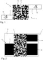
- Figure 1 shows in a first embodiment an optical component 1 according to the present invention.
- the optical component 1 can be arranged, for example, on a substrate 10.
- the substrate 10 contains a polymer.
- a film or a plate made of a polymer can be used as a substrate.
- the polymer can contain or consist of polymethyl methacrylate, polyester, polycarbonate or polyethylene, for example.
- the substrate can have a single-layer, homogeneous structure or several layers of the same or different materials arranged on top of one another. different materials.
- the substrate can be a polymer coating on a component or contain such a coating.
- the component itself can consist of a metal, an alloy, a glass or a ceramic or contain such a coating.
- the substrate has a first refractive index.
- first refractive index can be between 1.1 and approximately 1.6.
- second refractive index can be between approximately 1.7 and approximately 1.9.
- refractive index contrast i.e. a correspondingly large difference between the first and second refractive indices, is advantageous.
- the embodiment shown shows a digital metamaterial 2.
- the metamaterial 2 contains an array of individual pixels. For reasons of clarity, Figure 1 only 20x20 pixels are shown. In other embodiments of the invention, the number of pixels in the horizontal and/or vertical direction can also be larger or smaller. Also, individual pixels do not have to be Figure 1 shown as square. Other polygonal or round shapes are also conceivable.
- the depth of individual pixels within the substrate can extend over the entire material thickness of the substrate.
- the pixels may have a smaller depth.
- the Figure 1 The length or width shown in the horizontal and vertical directions may in some embodiments be between about 50 nm and about 800 nm. In general, the dimensions of a pixel will be smaller than the wavelength of optical signals processed by the optical component 1.
- the metamaterial 2 contains first pixels 21, which have a first refractive index, and second pixels 22, which have a second refractive index.
- First and second pixels can be arranged in a regular or irregular pattern within the array forming the metamaterial 2.
- the exact sequence of first and second pixels can be calculated, for example, in a simulation in order to achieve a desired behavior of the optical component 1.
- the optical component 1 can be used as a coupler which couples optical signals from one or more input waveguides to one or more output waveguides.
- the size, refractive indices and arrangement of the pixels 21 and 22 within the metamaterial 2 determine the behavior of a coupler formed in this way.
- the metamaterial 2 can be used as a sensor for temperature and/or mechanical stress or strain.
- the influence of the metamaterial 2 on an optical input signal changes depending on the thermal expansion or depending on the mechanical deformation due to a deformation of a component connected to the optical component.
- Figure 1 a single input waveguide 3 and a single output waveguide 4.
- Optical signals for example infrared light, are generated by means of an illumination device 30.
- the Illumination device 30 may comprise, for example, a light-emitting diode, a superluminescent diode or a semiconductor laser.
- the illumination device 30 may generate a modulated optical signal, wherein the modulation may represent data.
- the optical signal coupled into the metamaterial 2 via the input waveguide 3 interacts with the first pixels 21 and the second pixels 22 or at the interfaces formed between the first and second pixels 21 and 22. This can lead to interference, intensity changes and/or phase shifts.
- the electromagnetic signal modified in this way is fed to an output waveguide 4.
- the output waveguide 4 is connected to a schematically shown detection device 40.
- the detection device 40 can contain at least one photodiode in some embodiments. In other embodiments of the invention, the detection device 40 can contain at least two photodiodes, as will be described below with reference to the Figures 2 , 6 and 7 is explained.
- a photoresist or a UV-curing lacquer can be used to produce the metamaterial 2.
- the lacquer layer forms the substrate or a part of the substrate with the first refractive index. This can be 1.51, for example.
- the UV-curing lacquer is partially cured using a structured mask.
- a structured mask For example, microscope projection photolithography can be used for this.
- 2-photon photolithography, an embossing process or a direct inscription process using short-pulse laser radiation can be used.
- the UV-curing lacquer is then partially removed.
- the defects created in this way can be filled with a second polymer with a second refractive index.
- the second polymer can contain a dopant, for example nanoparticles which contain or consist of TiO 2 , for example.
- the second polymer can be polymethyl methacrylate, for example. In this way, the second refractive index can be 1.81, so that there is a sufficiently large contrast to the starting material.
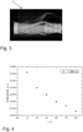
- FIG. 2 shows a second embodiment of an optical component according to the invention. Identical components of the invention are provided with the same reference numerals, so that the following description is limited to the essential differences.
- Figure 2 shows a substrate 10 on which a metamaterial 2 is formed. Light is supplied to the metamaterial 2 via an input waveguide 3. On the opposite side of the metamaterial 2 there are two output waveguides 4a and 4b.
- the output waveguide 4a has a smaller width so that it forms a single-mode waveguide.
- the waveguide 4b with a larger width, however, is a multimode waveguide like the input waveguide 3.
- the sequence of first and second pixels 21 and 22 of the metamaterial 2 is calculated in such a way that a predeterminable light intensity is coupled from the input waveguide 3 into the first output waveguide 4a. The remaining light intensity minus possible losses is coupled into the second output waveguide 4b.
- Both the first output waveguide 4a and the second output waveguide 4b are provided with detection devices, for example photodiodes.
- the optical component 1 shown can be used as an optical coupler or mode converter, which splits an input signal into two output signals.
- the optical component 1 can be used as a strain sensor. This is based on the knowledge that when the metamaterial 2 is stretched or compressed horizontally, its optical properties are changed in such a way that a larger or smaller proportion of the light is coupled into the first output waveguide 4a. Thus, by determining the intensity ratio in the output waveguides 4a and 4b, the strain acting on the metamaterial 2 can be determined.
- the mechanical stress or the force acting on the component can be determined.
- the optical measurement proposed according to the invention has a greater resistance to electromagnetic interference and can also be used in areas at risk of explosion.
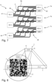
- Figure 3 shows a simulated wave field which is generated in an optical component according to the Figure 2 shown second embodiment.
- Figure 3 the intensity of the wave field is shown in the form of different brightness values.
- Figure 3 It can be seen that an input signal penetrates the metamaterial 2 through the input waveguide 3. The metamaterial causes a smaller proportion of between about 5% and about 15% of the intensity to couple into the first output waveguide 4a. The remaining intensity, minus any losses, is fed to the second output waveguide 4b.
- Figure 4 shows the intensity or the proportion of coupled light at the end of the first output waveguide 4a as a function of the elongation.
- the intensity of the mode coupled into the first output waveguide 4a is shown on the ordinate.
- the percentage elongation is on the abscissa.
- the simulation was carried out with infrared light at a wavelength of 850 nm.
- the intensity passing into the first output waveguide decreases with increasing strain. This results in a measuring range of low percentage strain, in which the decrease is disproportionate. This means that small strains in particular can be recorded with high accuracy. This is followed by an approximately linear range from around 3%. In this measuring range, the measurement signals can therefore be evaluated particularly easily after prior calibration.
- Figure 5 shows the intensity or the optical power of the light mode guided in the first output waveguide 4a on the ordinate against the strain on the abscissa. Simulation results are shown for three different wavelengths, namely 850 nm, 875 nm and 900 nm.
- Figure 6 shows a first embodiment of a sensor according to the invention for measuring mechanical stresses and/or temperatures.
- the sensor contains three optical components 1a, 1b and 1c, which can be arranged on a common substrate 10 (not shown in detail). Although only three optical components 1 are shown, the invention does not teach the use of exactly three optical components as a solution principle. Rather, the number of optical components in other embodiments of the invention can be greater or lesser and can be, for example, between 1 and about 20.
- each individual optical component 1a, 1b and 1c contains four metamaterials 2, which are each contacted by associated output waveguides 4a and 4b.
- the output waveguides 4a and 4b connect the metamaterials 2 to a photodiode array 41 and 42, which together form the detection device 40.
- the output waveguides 4a and 4b are arranged on different side edges of the metamaterial 2.
- the use of exactly four metamaterials 2 is to be understood as merely an example.
- the invention does not teach the use of exactly four metamaterials 2 as a solution principle. Rather, the number can be greater or lesser and can be between 1 and about 20.
- the substrate with the three optical components 1a, 1b and 1c and the total of 12 metamaterials 2 can be arranged on a mechanical component, for example a surface structure, a machine component, an aircraft wing, a body part or other components not mentioned here. If these components are subject to a change in shape due to the effect of mechanical loads or temperature changes, the metamaterials are also deformed. This is an essential Advantage of the inventive design of the metamaterials 2 on a polymer substrate. Previously known metamaterials that were made on silicon, on the other hand, cannot detect changes in shape. Rather, a change in shape of the underlying component would lead to the substrate breaking.
- the change in the longitudinal extension in one or both directions of the metamaterial 2 leads to a change in the intensities measured in the photodiode arrays 41 and 42. Due to the different channels of the photodiode array 41 or 42, the respective measured value can be assigned exactly to a metamaterial 2 and thus to a measuring location. In this way, deformations can be determined with pinpoint accuracy over large-area components.
- the optical interrogation signal used to determine the intensity or to determine the intensity ratio is in the embodiment according to Figure 6 along the normal vector of the plane defined by the metamaterial 2 of the control element 50.
- the lighting devices for example light-emitting diodes, are thus located, so to speak, above the substrate.
- FIG. 7 shows a second embodiment of a sensor according to the invention.
- the same components of the invention are provided with the same reference numerals, so that the following description focuses on the essential differences to the sensor shown in Figure 6 shown first embodiment.
- the illumination device 30 is located on or next to the substrate which accommodates the metamaterials 2.
- the light required to detect the deformation is thus supplied via input waveguides 3, which are arranged in the direction defined by the metamaterial 2 of the sensor element 50.
- One end of the input waveguide 3 is connected to the illumination device 30.
- FIG. 8 shows a strain sensor according to a third embodiment of the invention. Identical components of the invention are provided with the same reference numerals, so that the following description is limited to the essential differences.
- the third embodiment of the invention also contains a substrate (not shown) which contains or consists of a polymer.
- a metamaterial 2 with first pixels 21 and second pixels 22 is realized on the polymer by structuring as described above in at least one partial area or partial volume.
- at least one output waveguide 4 is located on the substrate.
- the output waveguide 4 contains a fluorescent dye. This fluorescent dye glows at a predeterminable fluorescence wavelength defined by the type of dye as soon as light of a longer wavelength is guided in the output waveguide 4.
- the intensity of the fluorescence signal scales with the intensity of the optical power guided in the output waveguide 4.
- Even if only a fluorescent dye is mentioned below, the invention can also be carried out with phosphorescent dyes or, generally speaking, with any material capable of luminescence.
- the term "fluorescence" in the sense of the present description is therefore to be interpreted broadly.
- the light required for signal generation is irradiated along the normal vector of the substrate or the optical metamaterial 2 produced thereon.
- the light of the illumination device 30 is emitted in the free beam the metamaterial 2.
- the illumination device 30 can contain a laser, in particular a semiconductor laser.
- the illumination device 30 can also have a lens or a lens system which focuses the light from a light source onto the substrate or the metamaterial 2.
- the light source can also contain an LED, an arc lamp or another light source known per se.
- the measurement signal can thus be recorded in a simple, contactless manner, for example by a camera system which uses a lens or a lens system to project the measurement signal onto a recording device which can contain, for example, an image intensifier tube, a CCD sensor, a CMOS sensor, a photodiode or a photodiode array.
- a recording device which can contain, for example, an image intensifier tube, a CCD sensor, a CMOS sensor, a photodiode or a photodiode array.
- the third embodiment of the invention thus allows a completely contactless recording of the measurement value, which can represent an expansion or compression of the metamaterial and thus a temperature and/or a mechanical stress.
- partial areas 7 can optionally be present, which are also provided with a fluorescent dye.
- the second fluorescent dye of the partial areas 7 can be different from the first Fluorescent dye of the output waveguide 4 can be different.
- the output waveguide 4 on the one hand and the partial areas 7 on the other hand light up with different wavelengths when excited by the identical light source, so that both fluorescence signals can be easily distinguished using wavelength multiplexing methods.
- the individual pixels or detection areas of the detection device can be divided into subpixels, which are preferably sensitive to light of either one or the other wavelength.
- the measurement signals of the partial areas 7 and the output waveguide 4 can alternatively or additionally be spatially separated.
- the at least one partial surface 7 is arranged at a distance from the metamaterial 2, so that optical signals between the metamaterial 2 and the partial surface 7 cannot couple or can only couple to a very small extent.
- the intensity of the fluorescence signal of the partial surface 7 thus represents a measure of the light impinging on the metamaterial 2, so that the measurement signal in the output waveguide 4 can be standardized to the incoming light intensity. This can increase the accuracy of the measurement or make it possible in the first place if the distance between the lighting device 40 and the metamaterial 2 fluctuates greatly.
- the substrate with the metamaterial 2, the output waveguide 4 and the optional partial surfaces 7 can thus be designed as a completely passive component without any further electrical or electronic components.
- a sensor can be produced inexpensively and can be particularly robust against environmental influences. For example, such sensors can be easily glued onto components to be monitored.
- the lighting device 40 required to record the measured values and the detection device 30 can be combined in a common reading device 6.
- the reading device 6 couples exclusively optically to the sensor according to the invention, so that the monitoring of mechanical components or the detection of the temperature is also possible through windows, for example if the component to be monitored is in a vacuum or in a corrosive environment.
- the reading device 6 can be designed as a handheld device or mounted on a tripod. The reading of a large number of sensors is also possible, for example if the components to be monitored move past the reading device 6 on a conveyor belt.
- large-area components for example membrane roofs, or elongated components, for example pipe systems or pipelines
- the reading device 6 can also be monitored in a simple manner if the reading device 6 is mounted on an unmanned flying object, for example a drone, which flies to and detects a plurality of sensors sequentially.
- the reading device 6 can be mounted on a vehicle which either travels on a rail running parallel to the pipe system or which uses the pipe to be monitored itself as a rail.
Landscapes
- Physics & Mathematics (AREA)
- General Physics & Mathematics (AREA)
- Optics & Photonics (AREA)
- Nonlinear Science (AREA)
- Engineering & Computer Science (AREA)
- Microelectronics & Electronic Packaging (AREA)
- Optical Integrated Circuits (AREA)
- Length Measuring Devices By Optical Means (AREA)
- Measuring Temperature Or Quantity Of Heat (AREA)
Description
- Die Erfindung betrifft eine optische Komponente mit einem Substrat mit einem ersten Brechungsindex, in welchem Raumbereiche mit einem zweiten Brechungsindex ausgebildet sind, wobei die optische Komponente zumindest ein optisches Metamaterial enthält, welches eine Mehrzahl einzelner Pixel enthält, welche jeweils einen Raumbereich umfassen, welcher den ersten oder den zweiten Brechungsindex aufweist. Weiterhin betrifft die Erfindung einen optischen Sensor, welcher zumindest eine der vorstehend beschriebenen optischen Komponenten enthält. Schließlich betrifft die Erfindung ein Verfahren zur Messung einer Dehnung und/oder eine Temperatur mit zumindest einer optischen Komponente, welche ein Substrat enthält, auf welchem Raumbereiche mit einem zweiten Brechungsindex ausgebildet sind. Vorrichtungen und Verfahren der eingangs genannten Art können beispielsweise als Koppler in der optischen Nachrichtentechnik oder als optischer Dehnungsmessstreifen zur Erfassung einer Temperatur und/oder einer Last eingesetzt werden.
- Aus B. Shen, P. Wang, R. Polson, R. Menon, Nature Photon. 9, 378 - 382 (2015) ist ein optisches Metamaterial der eingangs genannten Art bekannt. Dieses Metamaterial wird mit üblichen, aus der Halbleiterherstellung bekannten Lithografiemethoden in einem Siliziumsubstrat erzeugt. Dieses bekannte Material weist jedoch den Nachteil auf, dass Silizium energetisch aufwändig in der Herstellung ist. Weiterhin sind die Einsatzmöglichkeiten von Siliziumbauelementen begrenzt, da diese spröde sind und leicht brechen.
- Aus der
WO 2004/017111 A1 sind lichtempfindliche Polymermaterialien bekannt. Diese umfassen einen oder mehrere längliche Hohlräume, welche photonische Kristalle bilden. - Die
US 2009/0323014 A1 offenbart photonische Kristalle. Diese dienen der Verhinderung der Übertragung elektromagnetischer Strahlung von einer oder mehreren Laserquellen, um so eine optische Abschirmung zum Schutz der Augen eines Benutzers oder eines optischen Sensors bereitzustellen. - Die
US 2005/0117866 A1 zeigt ein Gerät, das auf einem flexiblen photonischen Kristall basiert, der aus einer periodischen Anordnung dielektrischen Materials mit hohem Brechungsindex besteht, das in ein flexibles Polymer eingebettet ist. - Aus Y. Yang, D. Yang, H. Tian, Y. Ji: Photoniccrystal stress sensor with high sensitivity in double directions based on shoulder-coupled aslant nanocavity. Sensors and Actuators A 193 (2013) 149 ist ein Sensor für mechanische Spannung bekannt.
- Ausgehend vom Stand der Technik liegt der Erfindung somit die Aufgabe zugrunde, eine optische Komponente anzugeben, welche neue Einsatzmöglichkeiten erschließt und/oder einen zuverlässigeren Betrieb ermöglicht und/oder welche einfacher und kostengünstiger herstellbar ist.
- Die Aufgabe wird erfindungsgemäß durch eine Vorrichtung gemäß Anspruch 1, einen optischen Sensor nach Anspruch 6 und ein Verfahren nach Anspruch 10 gelöst. Vorteilhafte Weiterbildungen der Erfindung finden sich in den Unteransprüchen.
- Erfindungsgemäß wird eine integrierte optische Komponente auf einem Substrat vorgeschlagen. Das Substrat weist einen ersten Brechungsindex auf, welcher eine Materialkonstante des für das Substrat verwendeten Materials darstellt.
- Durch Punkt-zu-Punkt-Belichten mit einem Kurzpulslaser, durch Belichten mit einer Maske, durch Dotierung oder durch andere, an sich bekannte Verfahren wird das Material des Substrates teilweise verändert, sodass sich Raumbereiche ausbilden, welche einen zweiten Brechungsindex aufweisen. Hierdurch können auf bzw. in dem Substrat Funktionsbereiche erzeugt werden, wie beispielsweise Wellenleiter, Koppler, Interferometer oder andere, an sich bekannte optische Bauelemente.
- Die erfindungsgemäße optische Komponente enthält zumindest einen Bereich, in welchem ein optisches Metamaterial ausgebildet wird. Unter einem Metamaterial werden für die Zwecke der vorliegenden Beschreibung Materialien verstanden, welche eine künstlich hergestellte Struktur enthalten, deren elektrische Permitivität und deren magnetische Permeabilität von den in der Natur üblichen Werten abweichen. Dies wird erreicht durch periodische, kleine Strukturen, welche im Inneren des Metamaterials ausgebildet werden. Vorliegend enthält das Metamaterial eine Mehrzahl einzelner Pixel, welche jeweils einen Raumbereich umfassen, welcher den ersten oder den zweiten Brechungsindex aufweist. Die Pixel können periodisch angeordnet sein, sodass sich quasi ein Schachbrettmuster ergibt, in welchem Pixel des einen und des anderen Brechungsindex abwechselnd angeordnet sind, wobei in den darunterliegenden Zeilen die Pixelfolge um eine Periode versetzt ist. In anderen Ausführungsformen der Erfindung können die Pixel ähnlich wie in einem optischen QR-Code in einem vorgebbaren, auf den ersten Blick willkürlichen Muster angeordnet sein, sodass sich eine gewünschte, vorgebbare Wirkung des Metamaterials auf optische Signale ergibt.
- Erfindungsgemäß wird nun vorgeschlagen, dass das Substrat zumindest ein Polymer enthält oder aus einem Polymer besteht. Dies ermöglicht einerseits eine einfachere und kostengünstigere Fertigung der optischen Komponente, beispielsweise durch Punkt-zu-Punkt-Belichten mit einem Kurzpulslaser. Der Kurzpulslaser kann in einigen Ausführungsformen der der Erfindung Pulse von weniger als 1 ns, weniger als 100 fs oder weniger als 10 fs aussenden. In anderen Ausführungsformen der Erfindung können mittels Laserstrahlung thermische Effekte in dem Material des Substrates erzeugt werden, welche zu einer Änderung des Brechungsindex führen. In wiederum anderen Ausführungsformen der Erfindung kann das Polymer des Substrates durch Maskieren und Ätzen teilweise entfernt und durch ein zweites Polymer ersetzt werden. Hierdurch können zum einen an sich bekannte optische Komponenten wie Wellenleiter, Koppler oder Interferometer im Substrat ausgebildet werden. In zumindest einer Teilfläche bzw. einem Teilvolumen des Substrates kann zusätzlich das erfindungsgemäße Metamaterial erzeugt werden, indem einzelne Pixel in der oben beschriebenen, gewünschten Abfolge erzeugt werden.
- Die erfindungsgemäße optische Komponente weist zudem den Vorteil auf, dass das Substrat eine im Vergleich zu Silizium größere thermische Ausdehnung aufweist. Hierdurch können sich bestimmte, vorgebbare Eigenschaften des Metamaterials ändern, sodass die optische Komponente zur Messung einer Temperatur herangezogen werden kann. In wiederum anderen Ausführungsformen der Erfindung kann das Substrat auf einer mechanischen Komponente bzw. einem mechanischen Bauteil befestigt sein, sodass bei einer Längenänderung des Bauteils auch eine Längenänderung des Substrates in zumindest einer Richtung erfolgt. Auch hierdurch können sich vorgebbare Eigenschaften des Metamaterials ändern, sodass die erfindungsgemäße optische Komponente als Sensor zur Messung einer Verformung und damit indirekt auch zur Messung einer einwirkenden Belastung bzw. Kraft verwendbar ist. Schließlich können mehrere Metamaterialien auf einem Substrat integriert sein, sodass unterschiedliche Belastungen bzw. unterschiedliche Belastungsrichtungen erfasst werden können oder Temperatur und einwirkende Last unabhängig voneinander bestimmbar sind.
- In einigen Ausführungsformen der Erfindung kann die Länge und/oder die Breite und/oder die Höhe eines Pixels kleiner sein als die Wellenlänge der optischen Signale, für deren Betrieb die optische Komponente eingerichtet ist. Hierdurch ist sichergestellt, dass die optischen Eigenschaften des Metamaterials in weiten Grenzen eingestellt werden können. Hierdurch kann das optische Signal nicht nur wie in konventionellen optischen Bauelementen fokussiert oder reflektiert werden, sondern auch gedehnt, verzerrt oder auf weitere Arten manipuliert werden.
- In einigen Ausführungsformen der Erfindung kann die Breite und/oder die Länge eines Pixels zwischen etwa 50 nm und etwa 800 nm oder zwischen etwa 200 nm und etwa 400 nm betragen. In einigen Ausführungsformen der Erfindung kann die Höhe eines Pixels zwischen etwa 0,5 µm und etwa 5 µm betragen. Dies erlaubt den Betrieb der optischen Komponente mit sichtbarem Licht oder mit Infrarotstrahlung. Insbesondere ist damit ein Betrieb der optischen Komponente mit den in der Telekommunikation gängigen Wellenlängen möglich, sodass erprobte und kostengünstige Lichtquellen und Detektoren zur Verfügung stehen.
- In einigen Ausführungsformen der Erfindung können die Pixel des Metamaterials in einem Array angeordnet sein. Dies erlaubt eine einfache Fertigung und eine diskrete Berechnung des Metamaterials, sodass eintreffende elektromagnetische Strahlung bzw. optische Signale in genau definierter Art und Weise manipuliert werden können.
- In einigen Ausführungsformen der Erfindung kann das Array in jeder Raumrichtung zwischen etwa 10 und etwa 1000 oder zwischen etwa 10 und etwa 200 oder zwischen etwa 100 und etwa 1000 oder zwischen etwa 150 und etwa 800 oder zwischen etwa 50 und etwa 500 Pixeln aufweisen. Metamaterialien in dieser Größe sind einerseits einfach herstellbar, gut in optischen Komponenten integrierbar und dazu geeignet, einen hinreichenden Effekt auf eintreffende elektromagnetische Strahlung auszuüben.
- Erfindungsgemäß beträgt der erste Brechungsindex zwischen etwa 1,0 und etwa 1,6 und der zweite Brechungsindex zwischen etwa 1,4 und etwa 1,9, wobei der zweite Brechungsindex größer ist als der erste Brechungsindex. Der Unterschied der Brechungsindices ist damit einerseits groß genug, um eine effiziente Führung optischer Signale in Wellenleiterstrukturen zu ermöglichen und andererseits Metamaterialien auszubilden, welche die gewünschte Manipulation der optischen Signale mit vergleichsweise einfachen Strukturen ermöglichen.
- In einigen Ausführungsformen der Erfindung kann das Substrat Polymethylmetacrylat und/oder ein Fotoresist enthalten. Solche Substrate können einfach bearbeitet werden und im Falle eines Fotoresists durch Beschichtung einer mechanischen Komponente bzw. eines Maschinenbauteils unmittelbar auf dem Bauteil erzeugt werden, dessen Eigenschaften bestimmt werden sollen.
- In einigen Ausführungsformen der Erfindung kann ein Teil der Pixel einen Dotierstoff und/oder Nanopartikel enthalten. Hierdurch kann sich der Brechungsindex des Substratmaterials ändern, sodass durch dotierte und undotierte Raumbereiche die Pixel mit erstem und zweitem Brechungsindex des Metamaterials erzeugt werden können.
- In einigen Ausführungsformen der Erfindung kann ein Teil der Pixel Titandioxid enthalten. Titandioxid als Nanopartikel ist einfach zu verarbeiten, ungiftig und führt zu einer hinreichend großen Änderung des Brechungsindex, sodass sich damit die erfindungsgemäßen optischen Komponenten besonders einfach herstellen lassen.
- In einigen Ausführungsformen der Erfindung wird ein erfindungsgemäßer Sensor dadurch ausgelesen, dass zumindest eine Beleuchtungseinrichtung mittels eines Eingangswellenleiters an das Sensorelement gekoppelt ist. Hierdurch kann ein optisches Abfragesignal von einer Lichtquelle, beispielsweise einem Laser, einer Leuchtdiode oder einer Superlumineszenzdiode in das als Sensorelement verwendete Metamaterial eingekoppelt werden.
- In einigen Ausführungsformen der Erfindung kann zumindest eine Nachweiseinrichtung mittels eines Ausgangswellenleiters an das Sensorelement gekoppelt sein. Als Nachweiseinrichtung kann beispielsweise ein Spektrometer oder eine Fotodiode verwendet werden.
- In einigen Ausführungsformen der Erfindung kann ein erfindungsgemäßer Sensor zumindest zwei Ausgangswellenleiter aufweisen, welche jeweils mit einer Fotodiode verbunden sind. Als Messsignal kann dann das Maß der Überkopplung eines über einen Eingangswellenleiter zugeführten optischen Signales in beide Ausgangswellenleiter herangezogen werden. Dieses lässt sich einfach durch Bestimmung des Intensitätsverhältnisses der zwei Fotodioden bestimmen.
- In einigen Ausführungsformen der Erfindung kann ein Ausgangswellenleiter ein Singlemode-Wellenleiter sein und ein Ausgangswellenleiter kann ein Multimode-Wellenleiter sein. Das als Sensorelement verwendete Metamaterial ist in diesen Fällen so gestaltet, dass ohne Einwirken einer Last ein vorgebbarer Anteil eines optischen Eingangssignals in den Singlemode-Wellenleiter überkoppelt. Bei Streckung bzw. Stauchung des Metamaterials durch einwirkende Kräfte und/oder Temperaturänderung verändert sich der Anteil des im Singlemode-Wellenleiter nachgewiesenen Lichtes, sodass das Intensitätsverhältnis zur Bestimmung von Kraft- und/oder Temperatur herangezogen werden kann.
- In einigen Ausführungsformen der Erfindung ist das Metamaterial dazu eingerichtet, zwischen etwa 1 % und etwa 20 % des über einen Eingangswellenleiter eingekoppelten Lichtes in einen Ausgangswellenleiter überzukoppeln, wobei zwischen etwa 90 % und etwa 10 % in den zweiten Ausgangswellenleiter einkoppeln. Dies erlaubt eine einfache Messung mit gutem Signal-/Rauschverhältnis und geringem apparativen Aufwand. In einigen Ausführungsformen der Erfindung kann das Verhältnis der Intensitäten der optischen Signale im ersten und zweiten Ausgangswellenleiter zwischen etwa 1:12 und etwa 1:4 betragen.
- In einigen Ausführungsformen der Erfindung kann die zur Auslese des verwendete Beleuchtungseinrichtung Licht mit einer Wellenlänge zwischen 500 nm, etwa 1000 nm aussenden. In anderen Ausführungsformen der Erfindung kann die Beleuchtungseinrichtung Licht mit einer Wellenlänge zwischen etwa 800 nm und etwa 950 nm aussenden. In einigen Ausführungsformend er Erfindung können Silicium-Photodioden als Nachweiseinrichtung verwendet werden.
- In einigen Ausführungsformen der Erfindung kann das Licht dem als Sensorelement verwendeten Metamaterial mittels eines Eingangswellenleiters zugeführt werden, welcher in der durch das Metamaterial definierten Ebene liegt.
- In anderen Ausführungsformen der Erfindung kann das Licht der Beleuchtungseinrichtung dem Sensorelement entlang des Normalenvektors der durch das Metamaterial definierten Ebene zugeführt werden. Dies erlaubt eine einfache Montage der Lichtquellen, welche in einem der Anordnung mehrerer Metamaterialien entsprechenden Raster auf einem zweiten Substrat angeordnet werden können, welches beispielsweise durch Flip-Chip-Bonden oder Klebung auf dem Substrat der Komponente angeordnet wird. In einigen Ausführungsformen kann die Lichtquelle beabstandet zum Metamaterial bzw. zum Polymersubstrat des Sensors angeordnet sein und beispielsweise einen Laser enthalten oder eine optische Linse aufweisen, um auf diese Weise das Messignal kontaktlos und ohne die Verwendung elektronischer Bauteile auf dem Messobjekt anzuregen.
- In einigen Ausführungsformen der Erfindung kann zumindest ein Ausgangswellenleiter einen ersten Fluoreszenzfarbstoff enthalten. Dieses Merkmal hat die Wirkung, dass das Messignal berührungslos anhand der Intensität des Floureszenssignals erfasst werden kann.
- In einigen Ausführungsformen der Erfindung kann auf dem Substrat des Sensors oder benachbart zum Sensor im Erfassungsbereich der Nachweiseinrichtung zumindest eine Teilfläche angeordnet ist, welche einen zweiten Fluoreszenzfarbstoff enthält. In einigen Ausführungsformen der Erfindung kann der zweite Fluoreszenzfarbstoff eine andere Fluoreszenzwellenlänge als der erste Fluoreszenzfarbstoff aufweisen. Durch die Messung der Intensität des Floureszenssignals des zweiten Fluoreszenzfarbstoffs kann dass Messsignal des Ausgangswellenleiters auf die eintreffende Intensität der Beleuchtungseinrichtung normiert werden.
- Nachfolgend soll die Erfindung anhand von Figuren ohne Beschränkung des allgemeinen Erfindungsgedankens näher erläutert werden. Dabei zeigt:
- Figur 1
- eine schematische Darstellung einer erfindungsgemäßen optischen Komponente in einer ersten Ausführungsform.
- Figur 2
- zeigt eine schematische Darstellung einer erfindungsgemäßen optischen Komponente in einer zweiten Ausführungsform.
- Figur 3
- zeigt Simulationsergebnisse des Verhaltens der optischen Komponente gemäß der zweiten Ausführungsform.
- Figur 4
- zeigt die Abhängigkeit des Intensitätsverhältnisses in den Ausgangswellenleitern bei horizontaler Dehnung der optischen Komponente gemäß
Figur 2 . - Figur 5
- zeigt die Wellenlängenabhängigkeit des Intensitätsverhältnisses in den Ausgangswellenleitern bei horizontaler Dehnung.
- Figur 6
- zeigt einen Dehnungssensor gemäß einer ersten Ausführungsform der Erfindung.
- Figur 7
- zeigt einen Dehnungssensor gemäß einer zweiten Ausführungsform der Erfindung.
- Figur 8
- zeigt einen Dehnungssensor gemäß einer dritten Ausführungsform der Erfindung.
-
Figur 1 zeigt in einer ersten Ausführungsform eine optische Komponente 1 gemäß der vorliegenden Erfindung. Die optische Komponente 1 kann beispielsweise auf einem Substrat 10 angeordnet sein. Das Substrat 10 enthält erfindungsgemäß ein Polymer. Beispielsweise kann eine Folie bzw. eine Platte aus einem Polymer als Substrat verwendet werden. Das Polymer kann beispielsweise Polymethylmetacrylat, Polyester, Polycarbonat oder Polyethylen enthalten oder daraus bestehen. Das Substrat kann einen einschichtigen, homogenen Aufbau aufweisen oder aber mehrere, aufeinander bzw. übereinander angeordnete Lagen gleicher oder unterschiedlicher Materialien enthalten. In einigen Ausführungsformen der Erfindung kann das Substrat eine Polymer-Beschichtung auf einem Bauteil sein bzw. eine solche Beschichtung enthalten. Das Bauteil selbst kann in diesen Fällen aus einem Metall, einer Legierung, einem Glas oder einer Keramik bestehen oder eine solche enthalten. - Das Substrat weist einen ersten Brechungsindex auf. Durch Dotieren, Materialmodifikation durch Laser- und/oder UV-Strahlung oder teilweises Entfernen des Materials des Substrates und Auffüllen mit einem anderen Material können im Substrat 10 Raumbereiche bzw. Flächenbereiche 12 ausgebildet werden, welche einen zweiten Brechungsindex aufweisen. In einigen Ausführungsformen der Erfindung kann der erste Brechungsindex zwischen 1,1 und etwa 1,6 betragen. Der zweite Brechungsindex kann zwischen etwa 1,7 und etwa 1,9 betragen. Selbstverständlich sind auch andere Ausführungsformen der Erfindung denkbar, in welchen die Brechungsindices von den genannten Werten abweichen. Vorteilhaft ist in einigen Ausführungsformen jedoch ein großer Brechungsindexkontrast, d.h. ein entsprechend großer Unterschied zwischen dem ersten und dem zweiten Brechungsindex.
- Durch die Änderung des Brechungsindex werden im Substrat 10 Strukturen gebildet, welche die optische Komponente bilden. In dem in
Figur 1 dargestellten Ausführungsbeispiel ist ein digitales Metamaterial 2 dargestellt. Das Metamaterial 2 enthält ein Array einzelner Pixel. Aus Gründen der Übersichtlichkeit sind inFigur 1 lediglich 20x20 Pixel dargestellt. In anderen Ausführungsformen der Erfindung kann die Anzahl der Pixel in horizontaler und/oder vertikaler Richtung auch größer bzw. kleiner sein. Auch müssen einzelne Pixel nicht wie inFigur 1 dargestellt quadratisch sein. Denkbar sind auch andere polygonale oder runde Formen. Die Tiefe einzelner Pixel innerhalb des Substrates können sich über die gesamte Materialstärke des Substrates erstrecken. - In anderen Ausführungsformen können die Pixel eine geringere Tiefe aufweisen. Die in
Figur 1 dargestellte Länge bzw. Breite in horizontaler und vertikaler Richtung kann in einigen Ausführungsformen zwischen etwa 50 nm und etwa 800 nm betragen. Im Allgemeinen werden die Abmessungen eines Pixels kleiner sein als die Wellenlänge optischer Signale, welche von der optischen Komponente 1 verarbeitet werden. - Wie in
Figur 1 dargestellt ist, enthält das Metamaterial 2 erste Pixel 21, welche einen ersten Brechungsindex aufweisen sowie zweite Pixel 22, welche einen zweiten Brechungsindex aufweisen. Erste und zweite Pixel können innerhalb des das Metamaterial 2 bildenden Arrays in einem regelmäßigen oder unregelmäßigen Muster angeordnet sein. Die genaue Abfolge erster und zweiter Pixel kann beispielsweise in einer Simulation berechnet werden, um ein gewünschtes Verhalten der optischen Komponente 1 zu erzielen. Beispielsweise kann die optische Komponente 1 als Koppler verwendet werden, welcher optische Signale von einem oder mehreren Eingangswellenleitern auf einen oder mehrere Ausgangswellenleiter überkoppelt. Größe, Brechungsindices und Anordnung der Pixel 21 und 22 innerhalb des Metamaterials 2 bestimmt dabei das Verhalten eines so gebildeten Kopplers. - In anderen Ausführungsformen der Erfindung kann das Metamaterial 2 als Sensor für Temperatur- und/oder mechanische Spannung bzw. Dehnung verwendet werden. In diesem Fall ändert sich der Einfluss des Metamaterials 2 auf ein optisches Eingangssignal in Abhängigkeit der thermischen Ausdehnung bzw. in Abhängigkeit der mechanischen Verformung aufgrund einer Verformung eines mit der optischen Komponente verbundenen Bauteils.
- Lediglich beispielhaft zeigt
Figur 1 einen einzigen Eingangswellenleiter 3 sowie einen einzigen Ausgangswellenleiter 4. Optische Signale, beispielsweise infrarotes Licht, werden mittels einer Beleuchtungseinrichtung 30 erzeugt. Die Beleuchtungseinrichtung 30 kann beispielsweise eine Leuchtdiode, eine Superlumineszenzdiode oder einen Halbleiterlaser umfassen. Die Beleuchtungseinrichtung 30 kann ein moduliertes optisches Signal erzeugen, wobei die Modulation Daten repräsentieren kann. - Das über den Eingangswellenleiter 3 in das Metamaterial 2 eingekoppelte optische Signal wechselwirkt mit den ersten Pixeln 21 und den zweiten Pixeln 22 bzw. an den zwischen den ersten und zweiten Pixeln 21 und 22 ausgebildeten Grenzflächen. Hierdurch kann es zu Interferenzen, Intensitätsänderungen und/oder Phasenverschiebungen kommen.
- Das solchermaßen modifizierte elektromagnetische Signal wird einem Ausgangswellenleiter 4 zugeführt. Der Ausgangswellenleiter 4 ist mit einer schematisch dargestellten Nachweiseinrichtung 40 verbunden. Die Nachweiseinrichtung 40 kann in einigen Ausführungsformen zumindest eine Fotodiode enthalten. In anderen Ausführungsformen der Erfindung kann die Nachweiseinrichtung 40 zumindest zwei Fotodioden enthalten, wie nachfolgend anhand den
Figuren 2 ,6 und7 erläutert wird. - Zur Herstellung des Metamaterials 2 kann in einigen Ausführungsformen der Erfindung ein Fotoresist bzw. ein UVhärtender Lack verwendet werden. Die Lackschicht bildet in diesen Fällen das Substrat bzw. einen Teil des Substrates mit dem ersten Brechungsindex. Dieser kann beispielsweise 1,51 betragen.
- Der UV-härtende Lack wird mit einer strukturierten Maske partiell ausgehärtet. Hierzu kann beispielsweise die Mikroskop-Projektions-Fotolithografie verwendet werden. Alternativ kann auch eine 2-Photonen-Fotolithografie, ein Prägeverfahren oder ein Direkt-Einschreib-Verfahren mittels Kurzpuls-Laserstrahlung verwendet werden.
- Nachfolgend wird der UV-härtende Lack teilweise entfernt. Die auf diese Weise entstehenden Fehlstellen können mit einem zweiten Polymer mit einem zweiten Brechungsindex aufgefüllt werden. In einigen Ausführungsformen der Erfindung kann das zweite Polymer einen Dotierstoff enthalten, beispielsweise Nanopartikel, welche beispielsweise TiO2 enthalten oder daraus bestehen. Das zweite Polymer kann beispielsweise Polymethylmetacrylat sein. Auf diese Weise kann der zweite Brechungsindex 1,81 betragen, sodass ein hinreichend großer Kontrast zum Ausgangsmaterial besteht.
-
Figur 2 zeigt eine zweite Ausführungsform einer erfindungsgemäßen optischen Komponente. Gleiche Bestandteile der Erfindung sind mit gleichen Bezugszeichen versehen, sodass sich die nachfolgende Beschreibung auf die wesentlichen Unterschiede beschränkt. - Auch
Figur 2 zeigt ein Substrat 10, auf welchem ein Metamaterial 2 ausgebildet ist. Dem Metamaterial 2 wird über einen Eingangswellenleiter 3 Licht zugeführt. Auf der gegenüberliegenden Seite des Metamaterials 2 befinden sich zwei Ausgangswellenleiter 4a und 4b. Der Ausgangswellenleiter 4a weist eine geringere Breite auf, sodass dieser einen Singlemode-Wellenleiter bildet. Der Wellenleiter 4b mit größerer Breite ist hingegen wie der Eingangswellenleiter 3 ein Multimode-Wellenleiter. - Die Abfolge erster und zweiter Pixel 21 und 22 des Metamaterials 2 ist so gerechnet, dass eine vorgebbare Lichtintensität vom Eingangswellenleiter 3 in den ersten Ausgangswellenleiter 4a überkoppelt. Die verbleibende Lichtintensität abzüglich eventueller Verluste koppelt in den zweiten Ausgangswellenleiter 4b.
- Sowohl der erste Ausgangswellenleiter 4a als auch der zweite Ausgangswellenleiter 4b sind mit Nachweiseinrichtungen, beispielsweise Fotodioden, verbunden. Somit kann die in
Figur 2 dargestellte optische Komponente 1 als optischer Koppler oder Modenkonverter verwendet werden, welcher ein Eingangssignal in zwei Ausgangssignale aufteilt. In anderen Ausführungsformen der Erfindung kann die optische Komponente 1 als Dehnungssensor verwendet werden. Dies beruht auf der Erkenntnis, dass bei horizontaler Dehnung bzw. Stauchung des Metamaterials 2 dessen optische Eigenschaften dahingehend geändert werden, dass ein größerer oder geringerer Anteil des Lichtes in den ersten Ausgangswellenleiter 4a überkoppelt. Somit kann durch Bestimmung des Intensitätsverhältnisses in den Ausgangswellenleitern 4a und 4b auf die auf das Metamaterial 2 einwirkende Dehnung geschlossen werden. Bei Kenntnis weiterer Parameter des mit dem Metamaterial 2 bzw. der optischen Komponente 1 versehenen Bauteils kann die auf das Bauteil einwirkende mechanische Spannung bzw. die einwirkende Kraft bestimmt werden. Im Gegensatz zu bekannten piezoelektrischen Dehnungssensoren weist die erfindungsgemäß vorgeschlagene optische Messung eine größere Resistenz gegen elektromagnetische Störungen auf und kann auch in explosionsgefährdeten Bereichen eingesetzt werden. -
Figur 3 zeigt ein simuliertes Wellenfeld, welches sich in einer optischen Komponente gemäß der inFigur 2 dargestellten zweiten Ausführungsform ausbilden kann. - In
Figur 3 ist die Intensität des Wellenfeldes in Form unterschiedlicher Helligkeitswerte dargestellt. AusFigur 3 ist ersichtlich, dass ein Eingangssignal durch den Eingangswellenleiter 3 in das Metamaterial 2 eindringt. Das Metamaterial führt dazu, dass ein geringerer Anteil zwischen etwa 5 % und etwa 15 % der Intensität in den ersten Ausgangswellenleiter 4a einkoppelt. Die verbleibende Intensität wird abzüglich eventueller Verluste dem zweiten Ausgangswellenleiter 4b zugeführt. -
Figur 4 zeigt die Intensität bzw. den Anteil eingekoppelten Lichtes am Ende des ersten Ausgangswellenleiters 4a in Abhängigkeit der Dehnung. Dabei ist die Intensität der in den ersten Ausgangswellenleiter 4a eingekoppelten Mode auf der Ordinate dargestellt. Die prozentuale Dehnung findet sich auf der Abszisse. Die Simulation erfolgte mit infrarotem Licht bei einer Wellenlänge von 850 nm. - Wie aus
Figur 4 ersichtlich ist, sinkt die in den ersten Ausgangswellenleiter übertretende Intensität mit zunehmender Dehnung ab. Dabei ergibt sich ein Messbereich geringer prozentualer Dehnung, in welchem der Abfall überproportional erfolgt. Somit können insbesondere geringe Dehnungen mit hoher Genauigkeit erfasst werden. Daran schließt sich ab etwa 3 % ein näherungsweise linearer Bereich an. In diesem Messbereich kann daher eine besonders einfache Auswertung der Messsignale nach vorheriger Kalibrierung erfolgen. - Auch
Figur 5 zeigt die Intensität bzw. die optische Leistung der im ersten Ausgangswellenleiter 4a geführten Lichtmode auf der Ordinate gegen die Dehnung auf die Abszisse. Dargestellt sind Simulationsergebnisse für drei verschiedene Wellenlängen, nämlich 850 nm, 875 nm und 900 nm. - Aus
Figur 5 ist ersichtlich, dass bei unterschiedlichen Wellenlängen die absolute Intensität im ersten Ausgangswellenleiter 4a variiert. Gleichwohl nimmt bei allen untersuchten Wellenlängen die Intensität mit zunehmender Dehnung ab, sodass Licht unterschiedlicher Wellenlängen verwendbar ist, um die gewünschten Messungen durchzuführen. -
Figur 6 zeigt ein erstes Ausführungsbeispiel eines erfindungsgemäßen Sensors zur Messung mechanischer Spannungen und/oder Temperaturen. Der Sensor enthält drei optische Komponenten 1a, 1b und 1c, welche auf einem gemeinsamen, nicht näher dargestellten Substrat 10 angeordnet sein können. Obgleich beispielhaft lediglich drei optische Komponenten 1 dargestellt sind, lehrt die Erfindung nicht die Verwendung von genau drei optischen Komponenten als Lösungsprinzip. Vielmehr kann die Anzahl der optischen Komponenten in anderen Ausführungsformen der Erfindung größer oder geringer sein und beispielsweise zwischen 1 und etwa 20 betragen. - Gleiche Bezugszeichen bezeichnen gleiche Bestandteile der Erfindung, sodass sich die nachfolgende Beschreibung auf die wesentlichen Unterschiede beschränkt.
- Jede einzelne optische Komponente 1a, 1b und 1c enthält im dargestellten Ausführungsbeispiel vier Metamaterialien 2, welche jeweils durch zugeordnete Ausgangswellenleiter 4a und 4b kontaktiert werden. Die Ausgangswellenleiter 4a und 4b verbinden die Metamaterialien 2 jeweils mit einem Fotodiodenarray 41 und 42, welche zusammen die Nachweiseinrichtung 40 bilden. Anders als bei der ersten und zweiten Ausführungsform gemäß
Figur 1 und 2 sind die Ausgangswellenleiter 4a und 4b an unterschiedlichen Seitenkanten des Metamaterials 2 angeordnet. Auch in diesem Fall ist die Verwendung von exakt vier Metamaterialien 2 lediglich beispielhaft zu verstehen. Auch in diesem Fall lehrt die Erfindung nicht die Verwendung von exakt vier Metamaterialien 2 als Lösungsprinzip. Vielmehr kann die Zahl größer oder geringer sein und zwischen 1 und etwa 20 betragen. - Das Substrat mit den drei optischen Komponenten 1a, 1b und 1c und den insgesamt 12 Metamaterialien 2 kann auf einer mechanischen Komponente angeordnet sein, beispielsweise einem Flächentragwerk, einem Maschinenbauteil, einer Tragfläche eines Flugzeugs, einem Karosserieteil oder anderen, hier nicht genannten Bauteilen. Sofern diese Bauteile durch Einwirkung mechanischer Lasten oder Temperaturänderungen einer Formänderung unterliegen, werden auch die Metamaterialien verformt. Dies ist ein wesentlicher Vorteil der erfindungsgemäßen Ausführung der Metamaterialien 2 auf einem Polymersubstrat. Bisher bekannte Metamaterialien, welche auf Silizium realisiert wurden, können demgegenüber keine Formänderungen erfassen. Vielmehr würde eine Formänderung des zugrundeliegenden Bauteils zum Bruch des Substrates führen.
- Wie bereits vorstehend beschrieben, führt die Änderung der Längsausdehnung in einer oder beiden Richtungen des Metamaterials 2 zu einer Änderung der in den Fotodiodenarrays 41 und 42 jeweils gemessenen Intensitäten. Durch die unterschiedlichen Kanäle des Fotodiodenarrays 41 bzw. 42 kann der jeweilige Messwert exakt einem Metamaterial 2 und damit einem Messort zugeordnet werden. Somit lassen sich Verformungen punktgenau über großflächige Bauteile bestimmen.
- Das zur Intensitätsbestimmung bzw. zur Bestimmung des Intensitätsverhältnisses verwendete optische Abfragesignal wird im Ausführungsbeispiel gemäß
Figur 6 entlang des normalen Vektors der durch das Metamaterial 2 des Steuerelementes 50 definierten Ebene zugeführt. Die Beleuchtungseinrichtungen, beispielsweise Leuchtdioden, sitzen somit gewissermaßen oberhalb des Substrates. -
Figur 7 zeigt eine zweite Ausführungsform eines erfindungsgemäßen Sensors. Gleiche Bestandteile der Erfindung sind mit gleichen Bezugszeichen versehen, sodass sich die nachfolgende Beschreibung auf die wesentlichen Unterschiede zu der inFigur 6 gezeigten ersten Ausführungsform beschränkt. - Wie aus
Figur 7 ersichtlich ist, befindet sich die Beleuchtungseinrichtung 30 auf bzw. neben dem Substrat, welches die Metamaterialien 2 aufnimmt. Die Zufuhr des zur Erfassung der Verformung notwendigen Lichtes erfolgt damit über Eingangswellenleiter 3, welche in der durch das Metamaterial 2 des Sensorelementes 50 definierten Ebene verlaufen. Ein Ende des Eingangswellenleiters 3 ist dabei mit der Beleuchtungseinrichtung 30 verbunden. -
Figur 8 zeigt einen Dehnungssensor gemäß einer dritten Ausführungsform der Erfindung. Gleiche Bestandteile der Erfindung sind mit gleichen Bezugszeichen versehen, sodass sich die nachfolgende Beschreibung auf die wesentlichen Unterschiede beschränkt. - Auch die dritte Ausführungsform der Erfindung enthält ein nicht dargestelltes Substrat, welches ein Polymer enthält oder daraus besteht. Auf dem Polymer ist durch Strukturierung wie vorstehend beschrieben in zumindest einer Teilfläche bzw. einen Teilvolumen ein Metamaterial 2 mit ersten Pixeln 21 und zweiten Pixeln 22 realisiert. Weiterhin befindet sich auf dem Substrat zumindest ein Ausgangswellenleiter 4. Der Ausgangswellenleiter 4 enthält einen Fluoreszenzfarbstoff. Dieser Fluoreszenzfarbstoff leuchtet bei einer vorgebbaren, durch die Art des Farbstoffes definierten Fluoreszenzwellenlänge, sobald Licht größerer Wellenlänge im Ausgangswellenleiter 4 geführt wird. Die Intensität des Fluoreszenzsignals skaliert dabei mit der Intensität der im Ausgangswellenleiter 4 geführten optischen Leistung. Auch wenn nachfolgend ausschließlich von einem Fluoreszenzfarbstoff die Rede ist, so kann die Erfindung auch mit phosphoreszierenden Farbstoffen oder allgemein gesprochen mit jedem zur Lumineszenz fähigen Material ausgeführt werden. Der Begriff "Fluoreszenz" im Sinne der vorliegenden Beschreibung ist somit entsprechend breit auszulegen.
- Wie bereits anhand der in
Figur 6 näher erläuterten ersten Ausführungsform eines Sensors wird das zur Signalerzeugung benötigte Licht entlang des Normalenvektors des Substrates bzw. des darauf erzeugten optischen Metamaterials 2 eingestrahlt. Im Unterschied zur ersten Ausführungsform wird jedoch das Licht der Beleuchtungseinrichtung 30 im Freistrahl dem Metamaterial 2 zugeführt. Hierzu kann die Beleuchtungseinrichtung 30 einen Laser enthalten, insbesondere einen Halbleiterlaser. Alternativ oder zusätzlich kann die Beleuchtungseinrichtung 30 auch eine Linse bzw. ein Linsensystem aufweisen, welches das Licht einer Lichtquelle auf das Substrat bzw. das Metamaterial 2 fokussiert. In diesem Fall kann die Lichtquelle auch eine LED, eine Bogenlampe oder eine andere, an sich bekannte Lichtquelle enthalten. - In Abhängigkeit der Dehnung bzw. Stauchung des Metamaterials 2 wird wiederum ein größerer oder geringerer Anteil des eintreffenden Lichtes in den Ausgangswellenleiter 4 eingekoppelt. Dieses Licht führt zur Anregung des Fluoreszenzfarbstoffes, sodass der Ausgangswellenleiter 4 bzw. die mit dem Farbstoff versehene Teilfläche des Ausgangswellenleiters 4 mit der durch den Farbstoff vorgegebenen Fluoreszenzwellenlänge leuchtet. Die Intensität dieses Leuchtens stellt das Messsignal dar.
- Das Messsignal kann somit in einfacher Weise berührungslos erfasst werden, beispielsweise durch ein Kamerasystem, welches mittels einer Linse oder eines Linsensystems das Messsignal auf eine Erfassungseinrichtung abbildet, welche beispielsweise eine Bildverstärkerröhre, einen CCD-Sensor, einen CMOS-Sensor, eine Fotodiode oder ein Fotodiodenarray enthalten kann. Die dritte Ausführungsform der Erfindung erlaubt somit eine vollständig berührungslose Erfassung des Messwertes, welcher eine Dehnung bzw. Stauchung des Metamaterials und damit eine Temperatur- und/oder eine mechanische Spannung repräsentieren kann.
- Zur Normierung des Fluoreszenzsignals des Ausgangswellenleiters 4 können optional Teilflächen 7 vorhanden sein, welche ebenfalls mit einem Fluoreszenzfarbstoff versehen sind. In einigen Ausführungsformen der Erfindung kann der zweite Fluoreszenzfarbstoff der Teilflächen 7 vom ersten Fluoreszenzfarbstoff des Ausgangswellenleiters 4 verschieden sein. Somit leuchten der Ausgangswellenleiter 4 einerseits und die Teilflächen 7 andererseits bei Anregung durch die identische Lichtquelle mit unterschiedlichen Wellenlängen, sodass beide Fluoreszenzsignale einfach durch Wellenlängenmultiplexverfahren unterschieden werden können. Hierzu können die einzelnen Pixel bzw. Erfassungsbereiche der Nachweiseinrichtung in Subpixel unterteilt sein, welche entweder für Licht der einen oder der anderen Wellenlänge bevorzugt sensitiv sind. In anderen Ausführungsformen der Erfindung kann alternativ oder zusätzlich eine räumliche Trennung der Messsignale der Teilflächen 7 und der Ausgangswellenleiter 4 erfolgen.
- Die zumindest eine Teilfläche 7 ist beabstandet zum Metamaterial 2 angeordnet, sodass optische Signale zwischen dem Metamaterial 2 und der Teilfläche 7 nicht oder nur in sehr geringem Maße überkoppeln können. Die Intensität des Fluoreszenzsignals der Teilfläche 7 stellt somit ein Maß für das auf das Metamaterial 2 auftreffende Licht dar, sodass das Messsignal im Ausgangswellenleiter 4 auf die eintreffende Lichtintensität normiert werden kann. Hierdurch kann die Genauigkeit der Messung erhöht sein oder bei stark schwankendem Abstand zwischen Beleuchtungseinrichtung 40 und Metamaterial 2 überhaupt erst ermöglicht werden.
- Das Substrat mit dem Metamaterial 2, dem Ausgangswellenleiter 4 und den optionalen Teilflächen 7 kann in der dritten Ausführungsform der Erfindung somit als vollständig passives Bauelement ohne weitere elektrische bzw. elektronische Komponenten ausgeführt sein. Ein solcher Sensor lässt sich kostengünstig produzieren und kann besonders robust gegenüber Umwelteinflüssen sein. Beispielsweise lassen sich solche Sensoren einfach auf zu überwachende Bauteile aufkleben.
- Die zur Erfassung der Messwerte erforderliche Beleuchtungseinrichtung 40 und die Nachweiseinrichtung 30 können in einem gemeinsamen Auslesegerät 6 zusammengefasst sein. Das Auslesegerät 6 koppelt ausschließlich optisch an den erfindungsgemäßen Sensor, sodass die Überwachung mechanischer Bauteile bzw. die Erfassung der Temperatur auch durch Fenster hindurch möglich ist, beispielsweise, wenn sich die zu überwachende Komponente im Vakuum oder in korrosiver Umgebung befindet. Hierzu kann das Auslesegerät 6 beispielsweise als Handgerät ausgeführt sein oder auf einem Stativ montiert werden. Auch die Auslese einer großen Anzahl von Sensoren ist somit möglich, beispielsweise wenn sich die zu überwachenden Komponenten auf einem Förderband am Auslesegerät 6 vorbeibewegen. Schließlich können auch großflächige Bauteile, beispielsweise Membrandächer, oder langgestreckte Bauteile, beispielsweise Rohrsysteme oder Pipelines, in einfacher Weise überwacht werden, wenn die Auslesegerät 6 auf einem unbemannten Flugobjekt montiert ist, beispielsweise einer Drohne, welche eine Mehrzahl von Sensoren sequenziell anfliegt und erfasst. In gleicher Weise kann das Auslesegerät 6 uf einem Fahrzeug montiert sein, welches entweder auf einer paralel zum Rohrsystem verlaufenden Schiene fährt oder das zu überwachende Rohr selbst als Schiene verwendet.
- Selbstverständlich ist die Erfindung nicht auf die dargestellten Ausführungsformen beschränkt. Die vorstehende Beschreibung ist daher nicht als beschränkend, sondern als erläuternd anzusehen. Die nachfolgenden Ansprüche sind so zu verstehen, dass ein genanntes Merkmal in zumindest einer Ausführungsform der Erfindung vorhanden ist. Dies schließt die Anwesenheit weiterer Merkmale nicht aus. Sofern die Ansprüche und die vorstehende Beschreibung "erste" und "zweite" Ausführungsformen definieren, so dient diese Bezeichnung der Unterscheidung zweier gleichartiger Ausführungsformen, ohne eine Rangfolge festzulegen.
Claims (15)
- Optische Komponente (1) geeignet zur Verwendung als Koppler zwischen Ein- und Ausgangswellenleitern oder in einem Sensor für Temperatur oder in Sensor für mechanische Spannung, aufweisend ein Substrat (10) mit einem ersten Brechungsindex, in welchem Raumbereiche (12) mit einem zweiten Brechungsindex ausgebildet sind, wobei die optische Komponente (1) zumindest ein optisches Metamaterial (2) enthält, welches eine Mehrzahl einzelner Pixel (21, 22) enthält, welche jeweils einen Raumbereich umfassen, welcher den ersten oder den zweiten Brechungsindex aufweist, wobei das Substrat (10) zumindest ein erstes Polymer mit einem ersten Brechungsindex enthält oder daraus besteht und die Raumbereiche (12) mit dem zweiten Brechungsindex durch Dotieren oder Materialmodifikation durch Laserstrahlung und/oder UV-Strahlung oder teilweises Entfernen des ersten Polymers durch Maskieren und Ätzen und Auffüllen mit einem zweiten Polymer ausgebildet sind, wobei der erste Brechungsindex zwischen 1,0 und 1,6 beträgt und der zweite Brechungsindex zwischen 1,4 und 1,9 beträgt und der zweite Brechungsindex größer ist als der erste Brechungsindex.
- Optische Komponente nach Anspruch 1, dadurch gekennzeichnet, dass die Länge und/oder die Breite und/oder die Höhe eines Pixels (21, 22) kleiner ist, als die Wellenlänge der optischen Signale, für deren Betrieb die optische Komponente eingerichtet ist.
- Optische Komponente nach einem der Ansprüche 1 bis 2, dadurch gekennzeichnet, dass das die Pixel (21, 22) des Metamaterials (2) in einem Array angeordnet sind, wobei optional das Array in jeder Raumrichtung zwischen 10 und 1000 oder zwischen 10 und 200 oder zwischen 100 und 1000 oder zwischen 150 und 800 oder zwischen 50 und 500 Pixeln aufweist und
dass optional ein Teil der Pixel (21, 22) einen Dotierstoff und/oder Nanopartikel enthalten. - Optische Komponente nach einem der Ansprüche 1 bis 3, dadurch gekennzeichnet, dass die Breite und/oder die Länge eines Pixels zwischen 50 nm und 800 nm oder zwischen 200 nm und 400 nm beträgt und/oder dass die Höhe eines Pixels zwischen 0,5 µm und 5 µm beträgt.
- Optische Komponente nach einem der Ansprüche 1 bis 4, dadurch gekennzeichnet, dass das Substrat (10) Polymethylmethacrylat und/oder einen Fotoresist enthält.
- Optischer Sensor (5) mit zumindest einem Sensorelement (50) und zumindest einer Beleuchtungseinrichtung (30), mit welchem dem Sensorelement Licht zuführbar ist, und mit zumindest einer Nachweiseinrichtung (40), mit welcher das vom Sensorelement ausgehende Licht analysierbar ist, dadurch gekennzeichnet, dass das Sensorelement (50) eine optische Komponente (1) nach einem der Ansprüche 1 bis 5 enthält.
- Sensor nach Anspruch 6, dadurch gekennzeichnet, dass zumindest eine Beleuchtungseinrichtung (30) mittels eines Eingangswellenleiters (3) an das Sensorelement (50) gekoppelt ist und/oder
dass zumindest eine Nachweiseinrichtung (40) mittels eines Ausgangswellenleiters (4) an das Sensorelement (50) gekoppelt ist. - Sensor nach einem der Ansprüche 6 oder 7, dadurch gekennzeichnet, dass die Nachweiseinrichtung (40) zumindest zwei Fotodioden (41, 42) enthält, welche mit je einem zugeordneten Ausgangswellenleiter (4a, 4b) an das Sensorelement (50) gekoppelt sind, oder
dass die Nachweiseinrichtung (40) zumindest zwei Fotodioden (41, 42) enthält, welche mit je einem zugeordneten Ausgangswellenleiter (4a, 4b) an das Sensorelement (50) gekoppelt sind, wobei einer der Ausgangswellenleiter (4a) ein Singlemode-Wellenleiter ist und der andere Ausgangswellenleiter (4b) ein Multimode-Wellenleiter ist. - Sensor nach einem der Ansprüche 6 bis 8, dadurch gekennzeichnet, dass zumindest ein Ausgangswellenleiter (4) einen ersten Fluoreszenzfarbstoff enthält und/oder dass auf dem Substrat (10) des Sensors zumindest eine Teilfläche angeordnet ist, welche einen zweiten Fluoreszenzfarbstoff enthält.
- Verfahren zur Messung einer Dehnung und/oder einer Temperatur mit zumindest einer optischen Komponente (1) nach einem der Ansprüche 1 bis 5, wobei mit zumindest einer Beleuchtungseinrichtung (30) dem Metamaterial (2) Licht zugeführt wird, und mit zumindest einer Nachweiseinrichtung (40),das vom Metamaterial (2) ausgehende Licht analysiert wird.
- Verfahren nach Anspruch 10, dadurch gekennzeichnet, dass die Beleuchtungseinrichtung (30) Licht mit einer Wellenlänge zwischen 500 nm und 1000 nm aussendet oder dass die Beleuchtungseinrichtung (30) Licht mit einer Wellenlänge zwischen 800 nm und 950 nm aussendet.
- Verfahren nach einem der Ansprüche 10 oder 11, dadurch gekennzeichnet, dass das Licht der Beleuchtungseinrichtung (30) in einer durch das Metamaterial (2) des Sensorelementes (50) definierten Ebene mittels eines Eingangswellenleiters (3) geführt wird oder dass das Licht der Beleuchtungseinrichtung (30) dem Sensorelement (50) entlang des Normalenvektors der durch das Metamaterial (2) des Sensorelementes (50) definierten Ebene zugeführt wird.
- Verfahren nach einem der Ansprüche 10 bis 12, dadurch gekennzeichnet, dass zumindest ein Ausgangswellenleiter (4) einen ersten Fluoreszenzfarbstoff enthält und mit zumindest einer Nachweiseinrichtung (40) die Intensität der Fluoreszenz bestimmt wird.
- Verfahren nach einem der Ansprüche 10 bis 13, dadurch gekennzeichnet, dass im Erfassungsbereich der Nachweiseinrichtung (40) zumindest eine Teilfläche (7) angeordnet ist, welche einen zweiten Fluoreszenzfarbstoff enthält, wobei aus der Intensität der Fluoreszenz der Teilfläche (7) die Intensität des Lichtes der Beleuchtungseinrichtung (30) bestimmt wird.
- Verfahren nach Anspruch 14, dadurch gekennzeichnet, dass die Trennung des Fluoreszenzsignals der Teilfläche (7) und des Ausgangswellenleiters (4) durch Wellenlängenmultiplex und/oder durch räumliche Trennung der Signale in der Nachweiseinrichtung (40) erfolgt.
Applications Claiming Priority (1)
| Application Number | Priority Date | Filing Date | Title |
|---|---|---|---|
| DE102016218067.3A DE102016218067B3 (de) | 2016-09-21 | 2016-09-21 | Optische Komponente, Sensor und Verfahren zur Messung einer Dehnung und/oder einer Temperatur |
Publications (3)
| Publication Number | Publication Date |
|---|---|
| EP3299850A2 EP3299850A2 (de) | 2018-03-28 |
| EP3299850A3 EP3299850A3 (de) | 2018-05-23 |
| EP3299850B1 true EP3299850B1 (de) | 2024-07-31 |
Family
ID=59119021
Family Applications (1)
| Application Number | Title | Priority Date | Filing Date |
|---|---|---|---|
| EP17189883.6A Active EP3299850B1 (de) | 2016-09-21 | 2017-09-07 | Optische komponente, sensor und verfahren zur messung einer dehnung und/oder einer temperatur |
Country Status (3)
| Country | Link |
|---|---|
| US (1) | US10557969B2 (de) |
| EP (1) | EP3299850B1 (de) |
| DE (1) | DE102016218067B3 (de) |
Families Citing this family (7)
| Publication number | Priority date | Publication date | Assignee | Title |
|---|---|---|---|---|
| DE102016218067B3 (de) * | 2016-09-21 | 2017-07-13 | Fraunhofer-Gesellschaft zur Förderung der angewandten Forschung e.V. | Optische Komponente, Sensor und Verfahren zur Messung einer Dehnung und/oder einer Temperatur |
| DE102017200840A1 (de) | 2017-01-19 | 2018-07-19 | Fraunhofer-Gesellschaft zur Förderung der angewandten Forschung e.V. | Optischer Isolationswächter und Verfahren zu dessen Verwendung und Herstellung |
| CN109059971B (zh) * | 2018-09-25 | 2024-04-30 | 桂林电子科技大学 | 一种三孔缝结构的传感器 |
| CN111983754B (zh) * | 2019-05-23 | 2021-10-26 | 上海交通大学 | 基于超表面结构的超紧凑硅波导模式转换器件 |
| KR102650663B1 (ko) * | 2021-09-15 | 2024-03-25 | 삼성전자주식회사 | 이미지 센서 및 이를 포함하는 전자 장치 |
| CN114019604B (zh) * | 2022-01-06 | 2022-05-17 | 浙江大学 | 一种小型波分解复用-复用器件 |
| US20240167815A1 (en) * | 2022-11-22 | 2024-05-23 | Infineon Technologies Ag | Metamaterial-based deformation sensing system |
Family Cites Families (7)
| Publication number | Priority date | Publication date | Assignee | Title |
|---|---|---|---|---|
| AU2002950855A0 (en) * | 2002-08-19 | 2002-09-12 | Swinburne University Of Technology | Materials |
| US7283716B2 (en) * | 2003-10-21 | 2007-10-16 | The Regents Of The University Of Colorado | Strain tunable, flexible photonic crystals |
| WO2007103560A2 (en) | 2006-03-08 | 2007-09-13 | Los Alamos National Security, Llc | Dynamical/tunable electromagnetic materials and devices |
| US7854505B2 (en) * | 2006-03-15 | 2010-12-21 | The Board Of Trustees Of The University Of Illinois | Passive and active photonic crystal structures and devices |
| US20100290503A1 (en) * | 2009-05-13 | 2010-11-18 | Prime Photonics, Lc | Ultra-High Temperature Distributed Wireless Sensors |
| EP2795300A1 (de) * | 2011-12-21 | 2014-10-29 | Imec | Optische fluoreszenzbasierte chemische und biochemische sensoren und verfahren zur herstellung solcher sensoren |
| DE102016218067B3 (de) * | 2016-09-21 | 2017-07-13 | Fraunhofer-Gesellschaft zur Förderung der angewandten Forschung e.V. | Optische Komponente, Sensor und Verfahren zur Messung einer Dehnung und/oder einer Temperatur |
-
2016
- 2016-09-21 DE DE102016218067.3A patent/DE102016218067B3/de active Active
-
2017
- 2017-09-07 EP EP17189883.6A patent/EP3299850B1/de active Active
- 2017-09-20 US US15/709,660 patent/US10557969B2/en active Active
Also Published As
| Publication number | Publication date |
|---|---|
| US10557969B2 (en) | 2020-02-11 |
| EP3299850A2 (de) | 2018-03-28 |
| US20180081081A1 (en) | 2018-03-22 |
| EP3299850A3 (de) | 2018-05-23 |
| DE102016218067B3 (de) | 2017-07-13 |
Similar Documents
| Publication | Publication Date | Title |
|---|---|---|
| DE102016218067B3 (de) | Optische Komponente, Sensor und Verfahren zur Messung einer Dehnung und/oder einer Temperatur | |
| EP0795121B1 (de) | Verfahren und vorrichtung zur messung von lichtbündeln | |
| EP2226648A2 (de) | 3D -Bilderzeugungssystem mit Multispektralsensor | |
| EP2885667B1 (de) | Planaroptisches element, sensorelement und verfahren zu dessen herstellung | |
| EP3204739B1 (de) | Vorrichtung zur spektrometrischen erfassung von licht mit einer photodiode, die monolithisch in die schichtstruktur eines wellenlängenselektiven filters integriert ist | |
| EP3201606B1 (de) | Vorrichtung und verfahren zur bestimmung einer brechzahl | |
| EP3642562B1 (de) | Kalibriernormal und verfahren zu seiner herstellung | |
| EP4115224B1 (de) | Lokalisierung von optischen koppelstellen | |
| DE102015214749B4 (de) | Vorrichtung und Verfahren zur Erfassung einer Last sowie mechanische Komponente | |
| DE19960370C2 (de) | Optischer Temperatursensor | |
| DD297521A5 (de) | Mikroskopisches verfahren und nahfeldreflexionsmikroskop | |
| DE102019220353A1 (de) | Verfahren zum Herstellen eines Kristallkörpers für eine Sensorvorrichtung und Sensorvorrichtung | |
| EP3783341A1 (de) | Gassensor und verfahren zur detektion eines zielgases | |
| DE112013001138T5 (de) | Vorrichtung zum Messen der Wärmebeabstrahlung eines Messobjekts, Verfahren zum Messen der Wärmeabstrahlung eines Messobjekts und Zelle zum Messen der Wärmeabstrahlung | |
| DE102016100220A1 (de) | Optische Vorrichtung zur Belichtung einer Sensorvorrichtung für ein Fahrzeug | |
| DE102020003758B4 (de) | Gitterteil und herstellungsverfahren hierfür | |
| WO2005012885A1 (de) | Berührungsloser optischer dehnungssensor zur messung von änderungen in der partikel plasmonenresonanz | |
| EP3172542B1 (de) | Anordnung zur orts- und wellenlängenaufgelösten erfassung von lichtstrahlung, die von mindestens einer oled oder led emittiert wird | |
| DE202010002129U1 (de) | Sensor zum Erfassen von Relativbewegungen zwischen Objekten | |
| EP3776028A1 (de) | Vorrichtung und verfahren zum übertragen von licht zwischen zumindest einem optoelektronischen bauelement und zumindest einem lichtwellenleiter | |
| DE102021127374A1 (de) | Sensor und Verfahren zur Bestimmung einer physikalischen Messgröße sowie Verfahren zur Herstellung eines solchen Sensors | |
| DE3645238C2 (de) | Optischer Sensor | |
| EP3338060B1 (de) | Optischer krümmungssensor | |
| EP2887038A1 (de) | Faseroptische Messvorrichtung | |
| DE102024138957B3 (de) | Verfahren zur Herstellung einer Struktur im Volumen eines zumindest teilweise transparenten Materials mittels eines Laserstrahls |
Legal Events
| Date | Code | Title | Description |
|---|---|---|---|
| PUAI | Public reference made under article 153(3) epc to a published international application that has entered the european phase |
Free format text: ORIGINAL CODE: 0009012 |
|
| STAA | Information on the status of an ep patent application or granted ep patent |
Free format text: STATUS: THE APPLICATION HAS BEEN PUBLISHED |
|
| AK | Designated contracting states |
Kind code of ref document: A2 Designated state(s): AL AT BE BG CH CY CZ DE DK EE ES FI FR GB GR HR HU IE IS IT LI LT LU LV MC MK MT NL NO PL PT RO RS SE SI SK SM TR |
|
| AX | Request for extension of the european patent |
Extension state: BA ME |
|
| PUAL | Search report despatched |
Free format text: ORIGINAL CODE: 0009013 |
|
| AK | Designated contracting states |
Kind code of ref document: A3 Designated state(s): AL AT BE BG CH CY CZ DE DK EE ES FI FR GB GR HR HU IE IS IT LI LT LU LV MC MK MT NL NO PL PT RO RS SE SI SK SM TR |
|
| AX | Request for extension of the european patent |
Extension state: BA ME |
|
| RIC1 | Information provided on ipc code assigned before grant |
Ipc: G01K 5/48 20060101ALI20180417BHEP Ipc: G02B 1/00 20060101AFI20180417BHEP Ipc: G02B 6/122 20060101ALI20180417BHEP Ipc: G01K 11/00 20060101ALI20180417BHEP |
|
| STAA | Information on the status of an ep patent application or granted ep patent |
Free format text: STATUS: REQUEST FOR EXAMINATION WAS MADE |
|
| 17P | Request for examination filed |
Effective date: 20181121 |
|
| RBV | Designated contracting states (corrected) |
Designated state(s): AL AT BE BG CH CY CZ DE DK EE ES FI FR GB GR HR HU IE IS IT LI LT LU LV MC MK MT NL NO PL PT RO RS SE SI SK SM TR |
|
| STAA | Information on the status of an ep patent application or granted ep patent |
Free format text: STATUS: EXAMINATION IS IN PROGRESS |
|
| 17Q | First examination report despatched |
Effective date: 20191024 |
|
| RAP3 | Party data changed (applicant data changed or rights of an application transferred) |
Owner name: FRAUNHOFER-GESELLSCHAFT ZUR FOERDERUNG DER ANGEWANDTEN FORSCHUNG E.V. |
|
| REG | Reference to a national code |
Ref legal event code: R079 Ipc: G02B0006125000 Ref country code: DE Ref legal event code: R079 Ref document number: 502017016299 Country of ref document: DE Free format text: PREVIOUS MAIN CLASS: G02B0001000000 Ipc: G02B0006125000 |
|
| GRAP | Despatch of communication of intention to grant a patent |
Free format text: ORIGINAL CODE: EPIDOSNIGR1 |
|
| STAA | Information on the status of an ep patent application or granted ep patent |
Free format text: STATUS: GRANT OF PATENT IS INTENDED |
|
| RIC1 | Information provided on ipc code assigned before grant |
Ipc: G01K 5/48 20060101ALI20240212BHEP Ipc: G02B 6/122 20060101ALI20240212BHEP Ipc: G01K 11/00 20060101ALI20240212BHEP Ipc: G02F 1/00 20060101ALI20240212BHEP Ipc: G01L 1/24 20060101ALI20240212BHEP Ipc: G02B 1/00 20060101ALI20240212BHEP Ipc: G01B 11/16 20060101ALI20240212BHEP Ipc: G02B 6/125 20060101AFI20240212BHEP |
|
| INTG | Intention to grant announced |
Effective date: 20240301 |
|
| GRAS | Grant fee paid |
Free format text: ORIGINAL CODE: EPIDOSNIGR3 |
|
| GRAA | (expected) grant |
Free format text: ORIGINAL CODE: 0009210 |
|
| STAA | Information on the status of an ep patent application or granted ep patent |
Free format text: STATUS: THE PATENT HAS BEEN GRANTED |
|
| AK | Designated contracting states |
Kind code of ref document: B1 Designated state(s): AL AT BE BG CH CY CZ DE DK EE ES FI FR GB GR HR HU IE IS IT LI LT LU LV MC MK MT NL NO PL PT RO RS SE SI SK SM TR |
|
| REG | Reference to a national code |
Ref country code: CH Ref legal event code: EP Ref country code: GB Ref legal event code: FG4D Free format text: NOT ENGLISH |
|
| REG | Reference to a national code |
Ref country code: DE Ref legal event code: R096 Ref document number: 502017016299 Country of ref document: DE |
|
| REG | Reference to a national code |
Ref country code: IE Ref legal event code: FG4D Free format text: LANGUAGE OF EP DOCUMENT: GERMAN |
|
| REG | Reference to a national code |
Ref country code: LT Ref legal event code: MG9D |
|
| REG | Reference to a national code |
Ref country code: NL Ref legal event code: MP Effective date: 20240731 |
|
| PG25 | Lapsed in a contracting state [announced via postgrant information from national office to epo] |
Ref country code: PT Free format text: LAPSE BECAUSE OF FAILURE TO SUBMIT A TRANSLATION OF THE DESCRIPTION OR TO PAY THE FEE WITHIN THE PRESCRIBED TIME-LIMIT Effective date: 20241202 |
|
| PG25 | Lapsed in a contracting state [announced via postgrant information from national office to epo] |
Ref country code: PT Free format text: LAPSE BECAUSE OF FAILURE TO SUBMIT A TRANSLATION OF THE DESCRIPTION OR TO PAY THE FEE WITHIN THE PRESCRIBED TIME-LIMIT Effective date: 20241202 |
|
| PG25 | Lapsed in a contracting state [announced via postgrant information from national office to epo] |
Ref country code: NO Free format text: LAPSE BECAUSE OF FAILURE TO SUBMIT A TRANSLATION OF THE DESCRIPTION OR TO PAY THE FEE WITHIN THE PRESCRIBED TIME-LIMIT Effective date: 20241031 |
|
| PG25 | Lapsed in a contracting state [announced via postgrant information from national office to epo] |
Ref country code: FI Free format text: LAPSE BECAUSE OF FAILURE TO SUBMIT A TRANSLATION OF THE DESCRIPTION OR TO PAY THE FEE WITHIN THE PRESCRIBED TIME-LIMIT Effective date: 20240731 Ref country code: PL Free format text: LAPSE BECAUSE OF FAILURE TO SUBMIT A TRANSLATION OF THE DESCRIPTION OR TO PAY THE FEE WITHIN THE PRESCRIBED TIME-LIMIT Effective date: 20240731 Ref country code: NL Free format text: LAPSE BECAUSE OF FAILURE TO SUBMIT A TRANSLATION OF THE DESCRIPTION OR TO PAY THE FEE WITHIN THE PRESCRIBED TIME-LIMIT Effective date: 20240731 Ref country code: GR Free format text: LAPSE BECAUSE OF FAILURE TO SUBMIT A TRANSLATION OF THE DESCRIPTION OR TO PAY THE FEE WITHIN THE PRESCRIBED TIME-LIMIT Effective date: 20241101 |
|
| PG25 | Lapsed in a contracting state [announced via postgrant information from national office to epo] |
Ref country code: BG Free format text: LAPSE BECAUSE OF FAILURE TO SUBMIT A TRANSLATION OF THE DESCRIPTION OR TO PAY THE FEE WITHIN THE PRESCRIBED TIME-LIMIT Effective date: 20240731 |
|
| PG25 | Lapsed in a contracting state [announced via postgrant information from national office to epo] |
Ref country code: LV Free format text: LAPSE BECAUSE OF FAILURE TO SUBMIT A TRANSLATION OF THE DESCRIPTION OR TO PAY THE FEE WITHIN THE PRESCRIBED TIME-LIMIT Effective date: 20240731 |
|
| PG25 | Lapsed in a contracting state [announced via postgrant information from national office to epo] |
Ref country code: IS Free format text: LAPSE BECAUSE OF FAILURE TO SUBMIT A TRANSLATION OF THE DESCRIPTION OR TO PAY THE FEE WITHIN THE PRESCRIBED TIME-LIMIT Effective date: 20241130 |
|
| PG25 | Lapsed in a contracting state [announced via postgrant information from national office to epo] |
Ref country code: HR Free format text: LAPSE BECAUSE OF FAILURE TO SUBMIT A TRANSLATION OF THE DESCRIPTION OR TO PAY THE FEE WITHIN THE PRESCRIBED TIME-LIMIT Effective date: 20240731 |
|
| PG25 | Lapsed in a contracting state [announced via postgrant information from national office to epo] |
Ref country code: RS Free format text: LAPSE BECAUSE OF FAILURE TO SUBMIT A TRANSLATION OF THE DESCRIPTION OR TO PAY THE FEE WITHIN THE PRESCRIBED TIME-LIMIT Effective date: 20241031 Ref country code: ES Free format text: LAPSE BECAUSE OF FAILURE TO SUBMIT A TRANSLATION OF THE DESCRIPTION OR TO PAY THE FEE WITHIN THE PRESCRIBED TIME-LIMIT Effective date: 20240731 |
|
| PG25 | Lapsed in a contracting state [announced via postgrant information from national office to epo] |
Ref country code: RS Free format text: LAPSE BECAUSE OF FAILURE TO SUBMIT A TRANSLATION OF THE DESCRIPTION OR TO PAY THE FEE WITHIN THE PRESCRIBED TIME-LIMIT Effective date: 20241031 Ref country code: PL Free format text: LAPSE BECAUSE OF FAILURE TO SUBMIT A TRANSLATION OF THE DESCRIPTION OR TO PAY THE FEE WITHIN THE PRESCRIBED TIME-LIMIT Effective date: 20240731 Ref country code: NO Free format text: LAPSE BECAUSE OF FAILURE TO SUBMIT A TRANSLATION OF THE DESCRIPTION OR TO PAY THE FEE WITHIN THE PRESCRIBED TIME-LIMIT Effective date: 20241031 Ref country code: NL Free format text: LAPSE BECAUSE OF FAILURE TO SUBMIT A TRANSLATION OF THE DESCRIPTION OR TO PAY THE FEE WITHIN THE PRESCRIBED TIME-LIMIT Effective date: 20240731 Ref country code: LV Free format text: LAPSE BECAUSE OF FAILURE TO SUBMIT A TRANSLATION OF THE DESCRIPTION OR TO PAY THE FEE WITHIN THE PRESCRIBED TIME-LIMIT Effective date: 20240731 Ref country code: IS Free format text: LAPSE BECAUSE OF FAILURE TO SUBMIT A TRANSLATION OF THE DESCRIPTION OR TO PAY THE FEE WITHIN THE PRESCRIBED TIME-LIMIT Effective date: 20241130 Ref country code: HR Free format text: LAPSE BECAUSE OF FAILURE TO SUBMIT A TRANSLATION OF THE DESCRIPTION OR TO PAY THE FEE WITHIN THE PRESCRIBED TIME-LIMIT Effective date: 20240731 Ref country code: GR Free format text: LAPSE BECAUSE OF FAILURE TO SUBMIT A TRANSLATION OF THE DESCRIPTION OR TO PAY THE FEE WITHIN THE PRESCRIBED TIME-LIMIT Effective date: 20241101 Ref country code: FI Free format text: LAPSE BECAUSE OF FAILURE TO SUBMIT A TRANSLATION OF THE DESCRIPTION OR TO PAY THE FEE WITHIN THE PRESCRIBED TIME-LIMIT Effective date: 20240731 Ref country code: ES Free format text: LAPSE BECAUSE OF FAILURE TO SUBMIT A TRANSLATION OF THE DESCRIPTION OR TO PAY THE FEE WITHIN THE PRESCRIBED TIME-LIMIT Effective date: 20240731 Ref country code: BG Free format text: LAPSE BECAUSE OF FAILURE TO SUBMIT A TRANSLATION OF THE DESCRIPTION OR TO PAY THE FEE WITHIN THE PRESCRIBED TIME-LIMIT Effective date: 20240731 |
|
| PG25 | Lapsed in a contracting state [announced via postgrant information from national office to epo] |
Ref country code: SM Free format text: LAPSE BECAUSE OF FAILURE TO SUBMIT A TRANSLATION OF THE DESCRIPTION OR TO PAY THE FEE WITHIN THE PRESCRIBED TIME-LIMIT Effective date: 20240731 Ref country code: RO Free format text: LAPSE BECAUSE OF FAILURE TO SUBMIT A TRANSLATION OF THE DESCRIPTION OR TO PAY THE FEE WITHIN THE PRESCRIBED TIME-LIMIT Effective date: 20240731 Ref country code: DK Free format text: LAPSE BECAUSE OF FAILURE TO SUBMIT A TRANSLATION OF THE DESCRIPTION OR TO PAY THE FEE WITHIN THE PRESCRIBED TIME-LIMIT Effective date: 20240731 |
|
| PG25 | Lapsed in a contracting state [announced via postgrant information from national office to epo] |
Ref country code: MC Free format text: LAPSE BECAUSE OF FAILURE TO SUBMIT A TRANSLATION OF THE DESCRIPTION OR TO PAY THE FEE WITHIN THE PRESCRIBED TIME-LIMIT Effective date: 20240731 Ref country code: EE Free format text: LAPSE BECAUSE OF FAILURE TO SUBMIT A TRANSLATION OF THE DESCRIPTION OR TO PAY THE FEE WITHIN THE PRESCRIBED TIME-LIMIT Effective date: 20240731 |
|
| PG25 | Lapsed in a contracting state [announced via postgrant information from national office to epo] |
Ref country code: CZ Free format text: LAPSE BECAUSE OF FAILURE TO SUBMIT A TRANSLATION OF THE DESCRIPTION OR TO PAY THE FEE WITHIN THE PRESCRIBED TIME-LIMIT Effective date: 20240731 |
|
| PG25 | Lapsed in a contracting state [announced via postgrant information from national office to epo] |
Ref country code: SK Free format text: LAPSE BECAUSE OF FAILURE TO SUBMIT A TRANSLATION OF THE DESCRIPTION OR TO PAY THE FEE WITHIN THE PRESCRIBED TIME-LIMIT Effective date: 20240731 Ref country code: IT Free format text: LAPSE BECAUSE OF FAILURE TO SUBMIT A TRANSLATION OF THE DESCRIPTION OR TO PAY THE FEE WITHIN THE PRESCRIBED TIME-LIMIT Effective date: 20240731 |
|
| REG | Reference to a national code |
Ref country code: CH Ref legal event code: PL |
|
| REG | Reference to a national code |
Ref country code: DE Ref legal event code: R097 Ref document number: 502017016299 Country of ref document: DE |
|
| PG25 | Lapsed in a contracting state [announced via postgrant information from national office to epo] |
Ref country code: LU Free format text: LAPSE BECAUSE OF NON-PAYMENT OF DUE FEES Effective date: 20240907 |
|
| PLBE | No opposition filed within time limit |
Free format text: ORIGINAL CODE: 0009261 |
|
| STAA | Information on the status of an ep patent application or granted ep patent |
Free format text: STATUS: NO OPPOSITION FILED WITHIN TIME LIMIT |
|
| 26N | No opposition filed |
Effective date: 20250501 |
|
| REG | Reference to a national code |
Ref country code: BE Ref legal event code: MM Effective date: 20240930 |
|
| PG25 | Lapsed in a contracting state [announced via postgrant information from national office to epo] |
Ref country code: BE Free format text: LAPSE BECAUSE OF NON-PAYMENT OF DUE FEES Effective date: 20240930 |
|
| PG25 | Lapsed in a contracting state [announced via postgrant information from national office to epo] |
Ref country code: CH Free format text: LAPSE BECAUSE OF NON-PAYMENT OF DUE FEES Effective date: 20240930 |
|
| PG25 | Lapsed in a contracting state [announced via postgrant information from national office to epo] |
Ref country code: IE Free format text: LAPSE BECAUSE OF NON-PAYMENT OF DUE FEES Effective date: 20240907 |
|
| PG25 | Lapsed in a contracting state [announced via postgrant information from national office to epo] |
Ref country code: SE Free format text: LAPSE BECAUSE OF FAILURE TO SUBMIT A TRANSLATION OF THE DESCRIPTION OR TO PAY THE FEE WITHIN THE PRESCRIBED TIME-LIMIT Effective date: 20240731 |
|
| PGFP | Annual fee paid to national office [announced via postgrant information from national office to epo] |
Ref country code: DE Payment date: 20250919 Year of fee payment: 9 |
|
| PGFP | Annual fee paid to national office [announced via postgrant information from national office to epo] |
Ref country code: GB Payment date: 20250923 Year of fee payment: 9 |
|
| PGFP | Annual fee paid to national office [announced via postgrant information from national office to epo] |
Ref country code: FR Payment date: 20250924 Year of fee payment: 9 |
|
| REG | Reference to a national code |
Ref country code: AT Ref legal event code: MM01 Ref document number: 1709006 Country of ref document: AT Kind code of ref document: T Effective date: 20240907 |
|
| PG25 | Lapsed in a contracting state [announced via postgrant information from national office to epo] |
Ref country code: AT Free format text: LAPSE BECAUSE OF NON-PAYMENT OF DUE FEES Effective date: 20240907 |
|
| PG25 | Lapsed in a contracting state [announced via postgrant information from national office to epo] |
Ref country code: CY Free format text: LAPSE BECAUSE OF FAILURE TO SUBMIT A TRANSLATION OF THE DESCRIPTION OR TO PAY THE FEE WITHIN THE PRESCRIBED TIME-LIMIT; INVALID AB INITIO Effective date: 20170907 |
|
| PG25 | Lapsed in a contracting state [announced via postgrant information from national office to epo] |
Ref country code: HU Free format text: LAPSE BECAUSE OF FAILURE TO SUBMIT A TRANSLATION OF THE DESCRIPTION OR TO PAY THE FEE WITHIN THE PRESCRIBED TIME-LIMIT; INVALID AB INITIO Effective date: 20170907 |