EP3299787A1 - Cmos and pressure sensor integrated on a chip and fabrication method - Google Patents
Cmos and pressure sensor integrated on a chip and fabrication method Download PDFInfo
- Publication number
- EP3299787A1 EP3299787A1 EP17181988.1A EP17181988A EP3299787A1 EP 3299787 A1 EP3299787 A1 EP 3299787A1 EP 17181988 A EP17181988 A EP 17181988A EP 3299787 A1 EP3299787 A1 EP 3299787A1
- Authority
- EP
- European Patent Office
- Prior art keywords
- cavity
- well region
- layer
- pressure sensor
- silicon layer
- Prior art date
- Legal status (The legal status is an assumption and is not a legal conclusion. Google has not performed a legal analysis and makes no representation as to the accuracy of the status listed.)
- Granted
Links
Images




Classifications
-
- G—PHYSICS
- G01—MEASURING; TESTING
- G01L—MEASURING FORCE, STRESS, TORQUE, WORK, MECHANICAL POWER, MECHANICAL EFFICIENCY, OR FLUID PRESSURE
- G01L9/00—Measuring steady of quasi-steady pressure of fluid or fluent solid material by electric or magnetic pressure-sensitive elements; Transmitting or indicating the displacement of mechanical pressure-sensitive elements, used to measure the steady or quasi-steady pressure of a fluid or fluent solid material, by electric or magnetic means
- G01L9/0041—Transmitting or indicating the displacement of flexible diaphragms
- G01L9/0042—Constructional details associated with semiconductive diaphragm sensors, e.g. etching, or constructional details of non-semiconductive diaphragms
-
- B—PERFORMING OPERATIONS; TRANSPORTING
- B81—MICROSTRUCTURAL TECHNOLOGY
- B81B—MICROSTRUCTURAL DEVICES OR SYSTEMS, e.g. MICROMECHANICAL DEVICES
- B81B3/00—Devices comprising flexible or deformable elements, e.g. comprising elastic tongues or membranes
- B81B3/0018—Structures acting upon the moving or flexible element for transforming energy into mechanical movement or vice versa, i.e. actuators, sensors, generators
- B81B3/0027—Structures for transforming mechanical energy, e.g. potential energy of a spring into translation, sound into translation
-
- B—PERFORMING OPERATIONS; TRANSPORTING
- B81—MICROSTRUCTURAL TECHNOLOGY
- B81C—PROCESSES OR APPARATUS SPECIALLY ADAPTED FOR THE MANUFACTURE OR TREATMENT OF MICROSTRUCTURAL DEVICES OR SYSTEMS
- B81C1/00—Manufacture or treatment of devices or systems in or on a substrate
- B81C1/00015—Manufacture or treatment of devices or systems in or on a substrate for manufacturing microsystems
- B81C1/00222—Integrating an electronic processing unit with a micromechanical structure
- B81C1/00246—Monolithic integration, i.e. micromechanical structure and electronic processing unit are integrated on the same substrate
-
- G—PHYSICS
- G01—MEASURING; TESTING
- G01L—MEASURING FORCE, STRESS, TORQUE, WORK, MECHANICAL POWER, MECHANICAL EFFICIENCY, OR FLUID PRESSURE
- G01L9/00—Measuring steady of quasi-steady pressure of fluid or fluent solid material by electric or magnetic pressure-sensitive elements; Transmitting or indicating the displacement of mechanical pressure-sensitive elements, used to measure the steady or quasi-steady pressure of a fluid or fluent solid material, by electric or magnetic means
- G01L9/0041—Transmitting or indicating the displacement of flexible diaphragms
- G01L9/0042—Constructional details associated with semiconductive diaphragm sensors, e.g. etching, or constructional details of non-semiconductive diaphragms
- G01L9/0045—Diaphragm associated with a buried cavity
-
- G—PHYSICS
- G01—MEASURING; TESTING
- G01L—MEASURING FORCE, STRESS, TORQUE, WORK, MECHANICAL POWER, MECHANICAL EFFICIENCY, OR FLUID PRESSURE
- G01L9/00—Measuring steady of quasi-steady pressure of fluid or fluent solid material by electric or magnetic pressure-sensitive elements; Transmitting or indicating the displacement of mechanical pressure-sensitive elements, used to measure the steady or quasi-steady pressure of a fluid or fluent solid material, by electric or magnetic means
- G01L9/0041—Transmitting or indicating the displacement of flexible diaphragms
- G01L9/0051—Transmitting or indicating the displacement of flexible diaphragms using variations in ohmic resistance
- G01L9/0052—Transmitting or indicating the displacement of flexible diaphragms using variations in ohmic resistance of piezoresistive elements
-
- G—PHYSICS
- G01—MEASURING; TESTING
- G01L—MEASURING FORCE, STRESS, TORQUE, WORK, MECHANICAL POWER, MECHANICAL EFFICIENCY, OR FLUID PRESSURE
- G01L9/00—Measuring steady of quasi-steady pressure of fluid or fluent solid material by electric or magnetic pressure-sensitive elements; Transmitting or indicating the displacement of mechanical pressure-sensitive elements, used to measure the steady or quasi-steady pressure of a fluid or fluent solid material, by electric or magnetic means
- G01L9/0041—Transmitting or indicating the displacement of flexible diaphragms
- G01L9/0051—Transmitting or indicating the displacement of flexible diaphragms using variations in ohmic resistance
- G01L9/0052—Transmitting or indicating the displacement of flexible diaphragms using variations in ohmic resistance of piezoresistive elements
- G01L9/0054—Transmitting or indicating the displacement of flexible diaphragms using variations in ohmic resistance of piezoresistive elements integral with a semiconducting diaphragm
-
- B—PERFORMING OPERATIONS; TRANSPORTING
- B81—MICROSTRUCTURAL TECHNOLOGY
- B81B—MICROSTRUCTURAL DEVICES OR SYSTEMS, e.g. MICROMECHANICAL DEVICES
- B81B2201/00—Specific applications of microelectromechanical systems
- B81B2201/02—Sensors
- B81B2201/0264—Pressure sensors
-
- B—PERFORMING OPERATIONS; TRANSPORTING
- B81—MICROSTRUCTURAL TECHNOLOGY
- B81B—MICROSTRUCTURAL DEVICES OR SYSTEMS, e.g. MICROMECHANICAL DEVICES
- B81B2203/00—Basic microelectromechanical structures
- B81B2203/01—Suspended structures, i.e. structures allowing a movement
- B81B2203/0127—Diaphragms, i.e. structures separating two media that can control the passage from one medium to another; Membranes, i.e. diaphragms with filtering function
-
- B—PERFORMING OPERATIONS; TRANSPORTING
- B81—MICROSTRUCTURAL TECHNOLOGY
- B81B—MICROSTRUCTURAL DEVICES OR SYSTEMS, e.g. MICROMECHANICAL DEVICES
- B81B2207/00—Microstructural systems or auxiliary parts thereof
- B81B2207/01—Microstructural systems or auxiliary parts thereof comprising a micromechanical device connected to control or processing electronics, i.e. Smart-MEMS
- B81B2207/015—Microstructural systems or auxiliary parts thereof comprising a micromechanical device connected to control or processing electronics, i.e. Smart-MEMS the micromechanical device and the control or processing electronics being integrated on the same substrate
-
- B—PERFORMING OPERATIONS; TRANSPORTING
- B81—MICROSTRUCTURAL TECHNOLOGY
- B81B—MICROSTRUCTURAL DEVICES OR SYSTEMS, e.g. MICROMECHANICAL DEVICES
- B81B2207/00—Microstructural systems or auxiliary parts thereof
- B81B2207/07—Interconnects
-
- B—PERFORMING OPERATIONS; TRANSPORTING
- B81—MICROSTRUCTURAL TECHNOLOGY
- B81C—PROCESSES OR APPARATUS SPECIALLY ADAPTED FOR THE MANUFACTURE OR TREATMENT OF MICROSTRUCTURAL DEVICES OR SYSTEMS
- B81C2201/00—Manufacture or treatment of microstructural devices or systems
- B81C2201/01—Manufacture or treatment of microstructural devices or systems in or on a substrate
- B81C2201/0101—Shaping material; Structuring the bulk substrate or layers on the substrate; Film patterning
- B81C2201/0128—Processes for removing material
- B81C2201/013—Etching
- B81C2201/0132—Dry etching, i.e. plasma etching, barrel etching, reactive ion etching [RIE], sputter etching or ion milling
-
- B—PERFORMING OPERATIONS; TRANSPORTING
- B81—MICROSTRUCTURAL TECHNOLOGY
- B81C—PROCESSES OR APPARATUS SPECIALLY ADAPTED FOR THE MANUFACTURE OR TREATMENT OF MICROSTRUCTURAL DEVICES OR SYSTEMS
- B81C2201/00—Manufacture or treatment of microstructural devices or systems
- B81C2201/05—Temporary protection of devices or parts of the devices during manufacturing
- B81C2201/053—Depositing a protective layers
-
- B—PERFORMING OPERATIONS; TRANSPORTING
- B81—MICROSTRUCTURAL TECHNOLOGY
- B81C—PROCESSES OR APPARATUS SPECIALLY ADAPTED FOR THE MANUFACTURE OR TREATMENT OF MICROSTRUCTURAL DEVICES OR SYSTEMS
- B81C2203/00—Forming microstructural systems
- B81C2203/07—Integrating an electronic processing unit with a micromechanical structure
- B81C2203/0707—Monolithic integration, i.e. the electronic processing unit is formed on or in the same substrate as the micromechanical structure
- B81C2203/0714—Forming the micromechanical structure with a CMOS process
Definitions
- the present invention relates generally to semiconductor devices and methods for making semiconductor devices. More specifically, the present invention relates to a complementary metal oxide semiconductor (CMOS) circuit and a pressure sensor integrated on a single substrate, both of which are concurrently fabricated using a CMOS fabrication process.
- CMOS complementary metal oxide semiconductor
- a piezoresistive pressure transducer includes a number of piezoresistors placed near the edge of a diaphragm where the stress change is high under external pressure. Accordingly, external pressure on the diaphragm stresses the diaphragm, which affects the resistance of the piezoresistors. The change in resistance can be detected by external circuitry, and the change in resistance is used to determine the pressure applied to the diaphragm.
- CMOS complementary metal oxide semiconductor
- CMOS fabrication process processes differences between a CMOS fabrication process and a piezoresistive pressure transducer fabrication process have complicated the development of a cost effective method for integrating a CMOS integrated circuit and a piezoresistive pressure transducer on a single chip.
- piezoresistive pressure devices consist of a separate CMOS signal processing die and a pressure sensor die co-packaged through wirebonding to form the pressure sensor system.
- Such a configuration has the disadvantages of more complicated packaging, relatively large footprint, and relatively high cost.
- ECE electrochemical etch
- embodiments disclosed herein entail a pressure sensor, a device that includes a pressure sensor integrated with a complementary metal oxide semiconductor (CMOS) integrated circuit on a single substrate, and methodology for concurrently fabricating the pressure sensor and the CMOS integrated circuit using a CMOS fabrication process.
- CMOS complementary metal oxide semiconductor
- the various inventive concepts and principles embodied herein enable the fabrication of an integrated pressure sensor and the CMOS integrated circuit to improve fabrication efficiency, simplify system packaging, minimize device footprint, improve device performance, and achieve cost savings.
- FIG. 1 shows a simplified side view of a device 20 that includes a complementary metal oxide semiconductor (CMOS) integrated circuit (IC) 22 and a pressure sensor 24 integrated on a single substrate 26.
- CMOS complementary metal oxide semiconductor
- IC complementary metal oxide semiconductor
- FIG. 1 shows a simplified side view of a device 20 that includes a complementary metal oxide semiconductor (CMOS) integrated circuit (IC) 22 and a pressure sensor 24 integrated on a single substrate 26.
- CMOS complementary metal oxide semiconductor
- IC complementary metal oxide semiconductor
- Dielectric structure 28 and metallization layers 32 of metallization structure 30 include electrically conductive material, referred to herein as electrical contacts 36, extending through them for carrying power and control signals to, as well as data output from, IC 22 and pressure sensor 24 in accordance with a particular design configuration.
- an exterior surface 38 of pressure sensor system 20 may include exterior structures 40, such as electrically conductive interconnects, ground traces, or bond pads (two example structures shown) that can be connected to various electrical contacts 36 in metallization structure 30.
- dielectric structure 28 and metallization structure 30 provides the signal and power routing between IC 22 and pressure sensor 24, as well as exterior to pressure sensor system 20.
- substrate 26 is a silicon-on-insulator (SOI) substrate.
- SOI substrate 26 includes a first silicon layer 42, a second silicon layer 44, and an insulator layer 46 interposed between first and second silicon layers 42, 44.
- a structural layer 48 is formed on first silicon layer 42 of SOI substrate 26.
- structural layer 48 may be an epitaxial layer having a first conductivity type (e.g., P type) fabricated in accordance with CMOS fabrication methodology.
- IC 22 is formed on first silicon layer 42 of SOI substrate 26 in structural layer 48 again in accordance with CMOS fabrication methodology.
- IC 22 of pressure sensor system 20 is shown in highly simplified form with portions of a few transistors 50 separated by isolation structures 52. It should be readily apparent, however, that IC 22 may include a plurality of transistors 50 for implementing logic gates and other digital circuits in order to provide signal processing capability for pressure sensor 24. The detailed structure of IC 22 will not be described herein for brevity.
- Pressure sensor 24 is also formed on first silicon layer 42 of SOI substrate 26 in structural layer 48 again in accordance with CMOS fabrication methodology. Pressure sensor 24 may be electrically isolated from transistors 50 of IC 22 by isolation structures 52. Pressure sensor 24 generally includes a well region 54, having a first conductivity type (e.g., N type), formed in structural layer 48. Pressure sensor 24 further includes at least one piezoresistor 56 (two shown) and electrical contact regions 58 in well region 54. Electrical contact regions 58 (e.g., P+ type) electrically interconnect piezoresistors 56 to their respective electrical contacts 36 extending through metallization structure 30.
- first conductivity type e.g., N type
- a first cavity 60 extends through metallization structure 30 overlying well region 54. Electrical contacts 36 for pressure sensor 24 are laterally displaced away from first cavity 60. Additionally, a second cavity 62 extends through second silicon layer 44 of SOI substrate 26 and stops, in this example, at insulator layer 46 of SOI substrate 26. In other configurations, second cavity 62 extends through both of second silicon layer44 and insulator layer 46 and stops at first silicon layer 42. A dielectric material layer 64 may be formed over an exterior surface 66 of silicon layer 44. Thus, second cavity 62 also extends through dielectric material layer 64. Accordingly, the remaining portion of first silicon layer 42 and the portion of structural layer 48 having well region 54 and insulator layer 54 interposed between first and second cavities 60, 62 defines a diaphragm 68 of pressure sensor 24.
- a piezoresistive pressure transducer such as pressure sensor 24, may be formed in a Wheatstone bridge configuration that includes four piezoresistors 56. These four piezoresistors 56 are placed near the edge of diaphragm 68 where the stress change is high under external pressure. Accordingly, external pressure on the diaphragm 68 stresses diaphragm 68, which affects the resistance of the piezoresistors 56. In pressure sensor system 20, the change in resistance can be detected by IC 22, and IC 22 can utilize the change of resistance to determine the pressure applied to diaphragm 68. Although a configuration that includes four piezoresistors 56 is discussed herein, it should be understood that alternative embodiments may include fewer than or greater than four piezoresistors 56 configured in numerous ways.
- a shield layer 70 may be formed over well region 54 of diaphragm 68.
- Dielectric material is commonly used in semiconductor devices, such as in pressure sensor system 20, for isolation and charge shielding. Undesirable charge accumulation can occur on the surface of such a device coated with a dielectric material as well as on intermediate layers that are capacitively coupled to the surface. Such charge accumulation can occur during manufacturing of pressure sensor system 20 (e.g., through reactive ion etching and other steps employing electric fields). The accumulated charge can be responsible for deleterious effects including electric field offsets, thin oxide tunneling, oxide breakdown, the formation of conductive channels between transistor terminal junctions, and so forth. In this configuration, the accumulated charge may cause an undesirable charging effect on piezoresistors 56. Shield layer 70 can serve to shield piezoresistors 56 from an external charge effect during manufacturing and/or in use.
- IC 22 and pressure sensor 24 are formed on a single substrate SOI substrate 26 by implementing CMOS fabrication methodology.
- SOI substrate 26 is used as a starting material, and IC 22 and pressure sensor 24 are fabricated directly on first silicon layer 42 of SOI substrate 26.
- the structures of pressure sensor 24 are formed during the CMOS fabrication process.
- the CMOS backend metallization structure 30 that includes metallization layers 32 and dielectric layers 34 are removed from diaphragm 68 of pressure sensor 24 through the formation of first cavity 60. Removal of metallization structure 30 from diaphragm 68 reduces the thermal and stress impact resulting from metallization structure 30.
- second silicon layer 44 of SOI substrate 26 can be removed using, for example, a deep reactive ion etch (DRIE) process from the backside of pressure sensor system 20 with insulator layer 46 being used as the DRIE process etch stop.
- DRIE deep reactive ion etch
- FIG. 2 shows a flowchart of a fabrication process 72 for forming pressure sensor system 20 using CMOS fabrication methodology. That is, fabrication process 72 entails concurrent fabrication of IC 22 and pressure sensor 24 on a starting material of SOI substrate 26. Fabrication process 72 is described in connection with the fabrication of a single pressure sensor system 20 for simplicity of illustration. However, it should be apparent to those skilled in the art that the ensuing methodology may be executed to concurrently fabricate a plurality of pressure sensor systems 20 in a wafer level fabrication process.
- structural layer 48 is formed on first silicon layer 42 of SOI substrate 26.
- well region 54 for pressure sensor 24 is formed in structure layer 48.
- a block 78 also continues from block 74.
- CMOS integrated circuit 22 is fabricated. Fabrication details of IC 22 are not provided herein for brevity. Rather, block 76 and block 78 continue from block 74 to emphasize that the fabrication of IC 22 occurs concurrent with the fabrication of pressure sensor 24 using CMOS fabrication techniques.
- isolation structures 52 are formed to suitably electrically isolate the various structures of pressure sensor system 20 from one another.
- piezoresistors 56 are implanted or otherwise formed in well region 54.
- shield layer 70 is formed over well region 54, and at a block 86, contact regions 58 are formed in well region 54.
- fabrication process 72 merges at a block 88.
- dielectric structure 28 is formed over IC 22 and pressure sensor 24, and at a block 90, metallization structure 30 is formed over dielectric structure 28.
- first cavity 60 is formed extending through metallization structure 30 and dielectric structure 28 stopping at shield layer 70.
- a protective coating (if needed) may be applied in first cavity 60, over exterior surface 38, and over exterior structures 40.
- second cavity 62 is formed extending through dielectric material layer 64 and second silicon layer 44 stopping at insulator layer 46, thus forming diaphragm 68 of pressure sensor 24. Again, as mentioned above, second cavity 62 may further extend through insulator layer 46 to stop at first silicon layer 42 in alternative configurations.
- the protective coating is removed following formation of second cavity 62.
- Pressure sensor system 20 includes pressure sensor 24 configured to measure a differential pressure.
- pressure sensor 24 configured to measure a differential pressure.
- both sides of diaphragm 68 are exposed to external environments via first and second cavities 60, 62.
- design requirements may call for an absolute pressure sensor configuration in lieu of the differential pressure sensor configuration of FIG. 1 .
- fabrication process 72 continues with a block 100.
- second cavity 62 is suitably sealed.
- fabrication process 72 ends.
- FIG. 3 shows a side view of a starting material used to fabricate pressure sensor system 20. More particularly, FIG. 3 shows SOI substrate 26 having first and second silicon layers 42, 44 with insulator layer 46 interposed between first and second silicon layers 42, 44 as the starting material for pressure sensor system 20 ( FIG. 1 ).
- first silicon layer 42 may be a P-type silicon wafer over insulator layer 46, which is sometimes referred to as a buried oxide (i.e., BOX) layer.
- Second silicon layer 44 may be an N-type handle wafer.
- FIG. 4 shows a side view of a structure at an initial stage 102 of processing in accordance with fabrication process 72 ( FIG. 2 ).
- structural layer 48 is formed on SOI substrate 26.
- N-type buried layers 104 for transistors 50 may be formed by, for example, ion implantation into first silicon layer 42.
- structural layer 48 may be formed.
- structural layer 48 may be formed by a P-type epitaxial layer deposition process followed by an oxide growth process that leaves an oxide layer 106 over structural layer 48
- FIG. 5 shows a side view of the structure of FIG. 4 at a subsequent stage 108 of processing.
- well region 54 for pressure sensor 24 ( FIG. 1 ) is formed in structural layer 48.
- Well region 54 may be formed by, for example, a photolithography and N-well implantation process to produce well region 54 in the P-type epitaxial structural layer 48
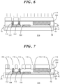
- FIG. 6 shows a side view of the structure of FIG. 5 at a subsequent stage 110 of processing.
- deep N+ type regions 112 may be implanted in P-type epitaxial structural layer 48 to make electrical contact with N-type buried layers 104.
- a photoresist 114 may be applied across the structure with openings in the photoresist 114 at which deep N+ type regions 112 are to be formed.
- an implantation process yields deep N+ type regions 112.
- FIG. 7 shows a side view of the structure of FIG. 6 at a subsequent stage 116 of processing.
- active area definition is performed.
- those regions at which other structures of IC 22 and pressure sensor 24 may be formed are defined and shallow trenches 118 are formed.
- shallow trenches 118 may be etched through photoresist 114, oxide layer 106 and into structural layer 48, well region 54, and N+ type regions 112.
- FIG. 8 shows a side view of the structure of FIG. 7 at a subsequent stage 120 of processing.
- isolation structures 52 are formed.
- photoresist 114 and oxide 106 FIG. 7
- various processes may be performed to fill shallow trenches 118 ( FIG. 7 ) with a sacrificial oxide 122, to hard mask shallow trenches 118 by nitride deposition followed by Tetraethyl Orthosilicate (TEOS) deposition, and to form deep trenches 124 through structural layer 48 and through insulator layer 46.
- Deep trenches 124 can be lined with an oxide material 126 and the lined deep trenches 124 may then be filled with, for example, polysilicon 128 to produce isolation structures 52. It should be understood that various alternative processes may be performed to produce isolation structures 52.
- FIG. 9 shows a side view of the structure of FIG. 8 at a subsequent stage 130 of processing.
- piezoresistors 56 are implanted in well region 54 for pressure sensor 24.
- a photoresist 132 may be applied across the structure with openings 134 in the photoresist 132 at which piezoresistors 56 are to be formed.
- an implantation process yields piezoresistors 56 in well region 54.
- FIG. 10 shows a side view of the structure of FIG. 9 at a subsequent stage 136 of processing.
- shield layer 70 is formed over well region 54 for pressure sensor 22.
- FIG. 10 It should be observed in FIG. 10 , that other structures of IC 22 ( FIG. 1 ) have been formed in the interim and concurrently with the formation of shield layer 70 for pressure sensor 24 in accordance with block 78 of fabrication process 72. The details of these additional structures are not described herein for brevity.
- FIG. 11 shows a side view of the structure of FIG. 10 at a subsequent stage 138 of processing.
- contact regions 58 are formed in well region 54 for pressure sensor 24 by, for example, photo PSD implant.
- Contact regions 58 e.g., P+ type
- P+ type contact regions will be used to electrically interconnect piezoresistors 56 to their respective electrical contacts 36 ( FIG. 1 ) extending through metallization structure 30 ( FIG. 1 ).
- FIG. 11 that other structures (e.g., P+ type contact regions) of IC 22 ( FIG. 1 ) have been formed in the interim and concurrently with the formation of contact regions 58 for pressure sensor 24 in accordance with block 78 of fabrication process 72. The details of these additional structures are not described herein for brevity.
- FIG. 12 shows a side view of the structure of FIG. 11 at a subsequent stage 140 of processing.
- dielectric structure 28 is formed over IC 22 and pressure sensor 24.
- a dielectric material 142 is deposited over IC 22 and pressure sensor 24.
- Electrical contacts 36 in the form of, for example, Tungsten or any other suitable material may be formed in dielectric material 142 per conventional CMOS processes. Electrical contacts 36 are electrically connected to contact regions 58 for pressure sensor 24 and other electrical contacts 36 may be suitably electrically connected to contact regions for IC 22.
- FIG. 13 shows a side view of the structure of FIG. 12 at a subsequent stage 142 of processing.
- metallization structure 30 is formed over IC 22 and pressure sensor 24.
- Metallization structure 30 can include multiple metallization layers 32.
- the various metallization layers 32 are formed from, for example, a TEOS insulator.
- Electrical contacts 36 which may be copper or any other suitable metal, are formed extending through the TEOS insulator of metallization layers 32.
- FIG. 14 shows a side view of the structure of FIG. 13 at a subsequent stage 144 of processing.
- Subsequent conventional CMOS processing operations may entail the formation of another metallization layer 32, followed by passivation layer 146, and formation of external structures 40.
- FIG. 15 shows a side view of the structure of FIG. 14 at a subsequent stage 148 of processing.
- first cavity 60 is formed extending through passivation layer 146, metallization structure 30, and dielectric structure 28 overlying well region 54 of pressure sensor 24. It should be observed that shield layer 70 for pressure sensor 24 is not removed during the formation of first cavity 60.
- FIG. 16 shows a side view of the structure of FIG. 15 at a subsequent stage 150 of processing.
- continued CMOS processing may entail backside grind and polish of second silicon layer 44, followed by deposition of dielectric material layer 64 (e.g., TEOS) on exterior surface 66 of second silicon layer 44.
- dielectric material layer 64 e.g., TEOS
- FIG. 17 shows a side view of the structure of FIG. 16 at a subsequent stage 152 of processing.
- a protective coating 154 may be applied in first cavity 60 and over exterior surface 38 of pressure sensor system 20.
- protective coating 154 may be used to provide front side protection of pressure sensor system 20 during the formation of second cavity 62 ( FIG. 1 ).
- FIG. 18 shows a side view of the structure of FIG. 17 at a subsequent stage 156 of processing.
- second cavity 62 is formed extending through dielectric material layer 64 and through second silicon layer 44 to yield diaphragm 68 of pressure sensor 24.
- Second cavity 62 may be formed using a deep reactive ion etch (DRIE) process.
- Insulator layer 46 is used as the DRIE etch stop.
- DRIE is a highly anisotropic etch process typically used to create deep penetration, steep-sided holes and trenches in wafers/substrates, typically with high aspect ratios. It is advantageous over an electrochemical etch (ECE) process in that an ECE process is typically a more complicated process and hence more costly to perform.
- ECE electrochemical etch
- FIG. 19 shows simplified a side view of a device 158 that includes CMOS IC 22 and pressure sensor 24 integrated on a single SOI substrate 26 in accordance with another embodiment.
- device 158 will be referred to hereinafter as pressure sensor system 158.
- pressure sensor system 20 FIG. 1
- pressure sensor system 20 FIG. 1
- Pressure sensor system 158 is configured as an absolute pressure sensor in lieu of the differential pressure sensor configuration of FIG. 1 .
- second cavity 62 is sealed.
- a second substrate 160 may be coupled to an outer surface of second silicon layer 44, and more particularly, to dielectric material layer 64 deposited on exterior surface 66 of second silicon layer 44 to seal second cavity 62.
- pressure sensor system 158 can be configured as an absolute pressure sensor system in which the pressure in second cavity 62 is constant, for example, at or near vacuum.
- a pressure sensor a pressure sensor system that includes a pressure sensor integrated with a complementary metal oxide semiconductor (CMOS) integrated circuit on a single substrate, and methodology for concurrently fabricating the pressure sensor and the CMOS integrated circuit using a CMOS fabrication process are disclosed herein.
- An embodiment of a device comprises a silicon-on-insulator (SOI) substrate, the SOI substrate having a first silicon layer, a second silicon layer, and an insulator layer interposed between the first and second silicon layers.
- SOI silicon-on-insulator
- the device further comprises a structural layer formed on the first silicon layer of the SOI substrate, the structural layer having a first conductivity type, a well region formed in the structural layer, the well region having a second conductivity type that is opposite from the first conductivity type, and at least one resistor in the well region.
- the device further comprises a metallization structure formed over the well region and the at least one resistor, a first cavity extending through the metallization structure overlying the well region, and a second cavity extending through the second silicon layer of the SOI substrate, the second cavity stopping at one of the first silicon layer and the insulator layer, wherein the well region interposed between the first and second cavities defines a diaphragm of a pressure sensor.
- the device further comprises a shield layer formed over the well region.
- the device further comprises electrical contacts in the metallization structure. The electrical contacts are electrically connected to the at least one resistor in the well region. The electrical contacts are laterally displaced away from the first cavity.
- the metallization structure includes multiple metallization layers and the first cavity extends through all of the metallization layers.
- the device further comprises a second substrate coupled to an outer surface of the second silicon layer. The second substrate seals the second cavity from an environment external to the device.
- the device further comprises a complementary metal oxide semiconductor, CMOS, integrated circuit on the first silicon layer of the SOI substrate. The CMOS integrated circuit is electrically isolated from the pressure sensor.
- CMOS complementary metal oxide semiconductor
- An embodiment of method of fabricating a pressure sensor comprises forming a structural layer on a first silicon layer of a silicon-on-insulator (SOI) substrate, the SOI substrate having the first silicon layer, a second silicon layer, and an insulator layer interposed between the first and second silicon layers, and the structural layer having a first conductivity type.
- SOI silicon-on-insulator
- the method further comprises forming a well region in the structural layer, the well region having a second conductivity type that is opposite from the first conductivity type, forming at least one resistor in the well region, forming a first cavity extending through the metallization structure overlying the well region, and forming a second cavity extending through the second silicon layer of the SOI substrate, the second cavity stopping at one of the first silicon layer and the insulator layer, wherein the well region interposed between the first and second cavities defines a diaphragm of the pressure sensor.
- the metallization structure includes multiple metallization layers.
- the first cavity extends through all of the metallization layers.
- the forming the second cavity comprises performing a deep reactive ion etch, DRIE, process to form the second cavity.
- the method of fabricating further comprises applying a protection coating in the first cavity and over an exterior surface of the metallization structure prior to the forming the second cavity; and removing the protection coating following formation of the second cavity.
- the method of fabricating further comprises sealing the second cavity from an external environment.
- the sealing comprises coupling a second substrate to an outer surface of the second silicon layer following formation of the second cavity.
- the method of fabricating further comprises forming a complementary metal oxide semiconductor, CMOS, integrated circuit (22) on the first silicon layer of the SOI substrate.
- CMOS complementary metal oxide semiconductor
- the forming the CMOS integrated circuit on the first silicon layer is performed concurrent with the forming the well region and the forming the at least one resistor.
- the method of fabricating further comprises forming an isolation structure between the pressure sensor and the CMOS integrated circuit. The isolation structure electrically isolates the CMOS integrated circuit from the pressure sensor.
- a device comprises a silicon-on-insulator (SOI) substrate, the SOI substrate having a first silicon layer, a second silicon layer, and an insulator layer interposed between the first and second silicon layers, and a structural layer formed on the first silicon layer of the SOI substrate, the structural layer having a first conductivity type.
- the device further comprises a pressure sensor having a well region and at least one resistor formed in the structural layer, a complementary metal oxide semiconductor (CMOS) integrated circuit on the first silicon layer of the SOI substrate in the structural layer, and metallization structure formed over the well region, the at least one resistor, and the CMOS integrated circuit.
- CMOS complementary metal oxide semiconductor
- a first cavity extends through the metallization structure overlying the well region and a second cavity extends through the second silicon layer of the SOI substrate, the second cavity stopping at one of the first silicon layer and the insulator layer, wherein the well region interposed between the first and second cavities defines a diaphragm of the pressure sensor.
- the device further comprises an isolation structure between the diaphragm of the pressure sensor and the CMOS integrated circuit.
- the isolation structure electrically isolating the CMOS integrated circuit from the pressure sensor.
- metallization structure includes electrical contacts. The electrical contacts are connected to the at least one resistor. The electrical contacts are laterally displaced away from the first cavity.
- the metallization structure includes multiple metallization layers. The first cavity extends through all of the metallization layers.
- the device further comprises a second substrate coupled to an outer surface of the second silicon layer. The second substrate seals the second cavity from an environment external to the device.
- the various inventive concepts and principles embodied herein enable the fabrication of an integrated pressure sensor and the CMOS integrated circuit to improve fabrication efficiency, simplify system packaging, minimize device footprint, improve device performance, and achieve cost savings.
Landscapes
- Engineering & Computer Science (AREA)
- Physics & Mathematics (AREA)
- General Physics & Mathematics (AREA)
- Chemical & Material Sciences (AREA)
- Analytical Chemistry (AREA)
- Manufacturing & Machinery (AREA)
- Microelectronics & Electronic Packaging (AREA)
- Computer Hardware Design (AREA)
- Pressure Sensors (AREA)
- Measuring Fluid Pressure (AREA)
Abstract
Description
- The present invention relates generally to semiconductor devices and methods for making semiconductor devices. More specifically, the present invention relates to a complementary metal oxide semiconductor (CMOS) circuit and a pressure sensor integrated on a single substrate, both of which are concurrently fabricated using a CMOS fabrication process.
- A piezoresistive pressure transducer includes a number of piezoresistors placed near the edge of a diaphragm where the stress change is high under external pressure. Accordingly, external pressure on the diaphragm stresses the diaphragm, which affects the resistance of the piezoresistors. The change in resistance can be detected by external circuitry, and the change in resistance is used to determine the pressure applied to the diaphragm.
- The miniaturization of sensors and electronic circuits is an ongoing effort for a multitude of applications in, for example, the consumer, industrial, medical, and automotive markets. Some miniaturized designs attempt to combine an application specific integrated circuit (ASIC) and a microelectromechanical systems (MEMS) sensor onto a single chip using, for example, a complementary metal oxide semiconductor (CMOS) fabrication process. A CMOS fabrication process can provide many logic gates and other digital circuits per unit area, is relatively inexpensive, and typically yields reliable circuits.
- Unfortunately, process differences between a CMOS fabrication process and a piezoresistive pressure transducer fabrication process have complicated the development of a cost effective method for integrating a CMOS integrated circuit and a piezoresistive pressure transducer on a single chip. Thus, many piezoresistive pressure devices consist of a separate CMOS signal processing die and a pressure sensor die co-packaged through wirebonding to form the pressure sensor system. Such a configuration has the disadvantages of more complicated packaging, relatively large footprint, and relatively high cost. Some prior art methods of integrating a CMOS signal processor and a pressure sensor on a single chip use an electrochemical etch (ECE) method to form a pressure sensor cavity. Such integration methods using ECE methodology have the disadvantages of relatively complicated processing and high cost.
- The accompanying figures in which like reference numerals refer to identical or functionally similar elements throughout the separate views, the figures are not necessarily drawn to scale, and which together with the detailed description below are incorporated in and form part of the specification, serve to further illustrate various embodiments and to explain various principles and advantages all in accordance with the present invention.
-
FIG. 1 shows a simplified side view of device that includes a complementary metal oxide semiconductor (CMOS) integrated circuit (IC) and a pressure sensor integrated on a single substrate; -
FIG. 2 shows a flowchart of a fabrication process for forming the device ofFIG. 1 using CMOS fabrication methodology; -
FIG. 3 shows a side view of a starting material used to fabricate the device ofFIG. 1 ; -
FIG. 4 shows a side view of a structure at an initial stage of processing in accordance with the fabrication process ofFIG. 2 ; -
FIG. 5 shows a side view of the structure ofFIG. 4 at a subsequent stage of processing; -
FIG. 6 shows a side view of the structure ofFIG. 5 at a subsequent stage of processing; -
FIG. 7 shows a side view of the structure ofFIG. 6 at a subsequent stage of processing; -
FIG. 8 shows a side view of the structure ofFIG. 7 at a subsequent stage of processing; -
FIG. 9 shows a side view of the structure ofFIG. 8 at a subsequent stage of processing; -
FIG. 10 shows a side view of the structure ofFIG. 9 at a subsequent stage of processing; -
FIG. 11 shows a side view of the structure ofFIG. 10 at a subsequent stage of processing; -
FIG. 12 shows a side view of the structure ofFIG. 11 at a subsequent stage of processing; -
FIG. 13 shows a side view of the structure ofFIG. 12 at a subsequent stage of processing; -
FIG. 14 shows a side view of the structure ofFIG. 13 at a subsequent stage of processing; -
FIG. 15 shows a side view of the structure ofFIG. 14 at a subsequent stage of processing; -
FIG. 16 shows a side view of the structure ofFIG. 15 at a subsequent stage of processing; -
FIG. 17 shows a side view of the structure ofFIG. 16 at a subsequent stage of processing; -
FIG. 18 shows a side view of the structure ofFIG. 17 at a subsequent stage of processing; and -
FIG. 19 shows simplified a side view of a device that includes a complementary metal oxide semiconductor (CMOS) integrated circuit (IC) and a pressure sensor integrated on a single substrate in accordance with another embodiment. - In overview, embodiments disclosed herein entail a pressure sensor, a device that includes a pressure sensor integrated with a complementary metal oxide semiconductor (CMOS) integrated circuit on a single substrate, and methodology for concurrently fabricating the pressure sensor and the CMOS integrated circuit using a CMOS fabrication process. The various inventive concepts and principles embodied herein enable the fabrication of an integrated pressure sensor and the CMOS integrated circuit to improve fabrication efficiency, simplify system packaging, minimize device footprint, improve device performance, and achieve cost savings.
- The instant disclosure is provided to further explain in an enabling fashion the best modes, at the time of the application, of making and using various embodiments in accordance with the present invention. The disclosure is further offered to enhance an understanding and appreciation for the inventive principles and advantages thereof, rather than to limit in any manner the invention. The invention is defined solely by the appended claims including any amendments made during the pendency of this application and all equivalents of those claims as issued.
- It should be understood that the use of relational terms, if any, such as first and second, top and bottom, and the like may be used herein solely to distinguish one from another entity or action without necessarily requiring or implying any actual such relationship or order between such entities or actions. Furthermore, some of the figures may be illustrated using various shading and/or hatching to distinguish the different elements produced within the various structural layers. These different elements within the structural layers may be produced utilizing current and upcoming microfabrication techniques of depositing, patterning, etching, and so forth. Accordingly, although different shading and/or hatching is utilized in the illustrations, the different elements within the structural layers may be formed out of the same material.
- Referring to
FIG. 1, FIG. 1 shows a simplified side view of adevice 20 that includes a complementary metal oxide semiconductor (CMOS) integrated circuit (IC) 22 and apressure sensor 24 integrated on asingle substrate 26. Thus,device 20 will be referred to herein as apressure sensor system 20. Adielectric structure 28 and ametallization structure 30 are formed overIC 22 andpressure sensor 24. Metallization structure 30 (sometimes referred to as inter metal dielectric layers) is in the form ofmultiple metallization layers 32.Dielectric structure 28 andmetallization layers 32 ofmetallization structure 30 include electrically conductive material, referred to herein aselectrical contacts 36, extending through them for carrying power and control signals to, as well as data output from,IC 22 andpressure sensor 24 in accordance with a particular design configuration. Thus, anexterior surface 38 ofpressure sensor system 20 may includeexterior structures 40, such as electrically conductive interconnects, ground traces, or bond pads (two example structures shown) that can be connected to variouselectrical contacts 36 inmetallization structure 30. Accordingly,dielectric structure 28 andmetallization structure 30 provides the signal and power routing betweenIC 22 andpressure sensor 24, as well as exterior topressure sensor system 20. - In accordance with a particular embodiment,
substrate 26 is a silicon-on-insulator (SOI) substrate.SOI substrate 26 includes afirst silicon layer 42, asecond silicon layer 44, and aninsulator layer 46 interposed between first andsecond silicon layers structural layer 48 is formed onfirst silicon layer 42 ofSOI substrate 26. As will be described in significantly greater detail below,structural layer 48 may be an epitaxial layer having a first conductivity type (e.g., P type) fabricated in accordance with CMOS fabrication methodology. - IC 22 is formed on
first silicon layer 42 ofSOI substrate 26 instructural layer 48 again in accordance with CMOS fabrication methodology. IC 22 ofpressure sensor system 20 is shown in highly simplified form with portions of afew transistors 50 separated byisolation structures 52. It should be readily apparent, however, that IC 22 may include a plurality oftransistors 50 for implementing logic gates and other digital circuits in order to provide signal processing capability forpressure sensor 24. The detailed structure ofIC 22 will not be described herein for brevity. -
Pressure sensor 24 is also formed onfirst silicon layer 42 ofSOI substrate 26 instructural layer 48 again in accordance with CMOS fabrication methodology.Pressure sensor 24 may be electrically isolated fromtransistors 50 ofIC 22 byisolation structures 52.Pressure sensor 24 generally includes awell region 54, having a first conductivity type (e.g., N type), formed instructural layer 48.Pressure sensor 24 further includes at least one piezoresistor 56 (two shown) andelectrical contact regions 58 inwell region 54. Electrical contact regions 58 (e.g., P+ type) electrically interconnectpiezoresistors 56 to their respectiveelectrical contacts 36 extending throughmetallization structure 30. - A
first cavity 60 extends throughmetallization structure 30overlying well region 54.Electrical contacts 36 forpressure sensor 24 are laterally displaced away fromfirst cavity 60. Additionally, asecond cavity 62 extends throughsecond silicon layer 44 ofSOI substrate 26 and stops, in this example, atinsulator layer 46 ofSOI substrate 26. In other configurations,second cavity 62 extends through both of second silicon layer44 andinsulator layer 46 and stops atfirst silicon layer 42. Adielectric material layer 64 may be formed over anexterior surface 66 ofsilicon layer 44. Thus,second cavity 62 also extends throughdielectric material layer 64. Accordingly, the remaining portion offirst silicon layer 42 and the portion ofstructural layer 48 havingwell region 54 andinsulator layer 54 interposed between first andsecond cavities diaphragm 68 ofpressure sensor 24. - A piezoresistive pressure transducer, such as
pressure sensor 24, may be formed in a Wheatstone bridge configuration that includes fourpiezoresistors 56. These fourpiezoresistors 56 are placed near the edge ofdiaphragm 68 where the stress change is high under external pressure. Accordingly, external pressure on thediaphragm 68 stresses diaphragm 68, which affects the resistance of thepiezoresistors 56. Inpressure sensor system 20, the change in resistance can be detected byIC 22, andIC 22 can utilize the change of resistance to determine the pressure applied todiaphragm 68. Although a configuration that includes fourpiezoresistors 56 is discussed herein, it should be understood that alternative embodiments may include fewer than or greater than fourpiezoresistors 56 configured in numerous ways. - In some embodiments, a
shield layer 70 may be formed overwell region 54 ofdiaphragm 68. Dielectric material is commonly used in semiconductor devices, such as inpressure sensor system 20, for isolation and charge shielding. Undesirable charge accumulation can occur on the surface of such a device coated with a dielectric material as well as on intermediate layers that are capacitively coupled to the surface. Such charge accumulation can occur during manufacturing of pressure sensor system 20 (e.g., through reactive ion etching and other steps employing electric fields). The accumulated charge can be responsible for deleterious effects including electric field offsets, thin oxide tunneling, oxide breakdown, the formation of conductive channels between transistor terminal junctions, and so forth. In this configuration, the accumulated charge may cause an undesirable charging effect onpiezoresistors 56.Shield layer 70 can serve to shieldpiezoresistors 56 from an external charge effect during manufacturing and/or in use. - In accordance with an embodiment,
IC 22 andpressure sensor 24 are formed on a singlesubstrate SOI substrate 26 by implementing CMOS fabrication methodology.SOI substrate 26 is used as a starting material, andIC 22 andpressure sensor 24 are fabricated directly onfirst silicon layer 42 ofSOI substrate 26. In particular, the structures ofpressure sensor 24 are formed during the CMOS fabrication process. The CMOSbackend metallization structure 30 that includes metallization layers 32 and dielectric layers 34 are removed fromdiaphragm 68 ofpressure sensor 24 through the formation offirst cavity 60. Removal ofmetallization structure 30 fromdiaphragm 68 reduces the thermal and stress impact resulting frommetallization structure 30. As will be discussed below,second silicon layer 44 ofSOI substrate 26 can be removed using, for example, a deep reactive ion etch (DRIE) process from the backside ofpressure sensor system 20 withinsulator layer 46 being used as the DRIE process etch stop. Thus,diaphragm 68 is produced from the material remaining following formation of first andsecond cavities - Referring to
FIGs. 1 and2, FIG. 2 shows a flowchart of afabrication process 72 for formingpressure sensor system 20 using CMOS fabrication methodology. That is,fabrication process 72 entails concurrent fabrication ofIC 22 andpressure sensor 24 on a starting material ofSOI substrate 26.Fabrication process 72 is described in connection with the fabrication of a singlepressure sensor system 20 for simplicity of illustration. However, it should be apparent to those skilled in the art that the ensuing methodology may be executed to concurrently fabricate a plurality ofpressure sensor systems 20 in a wafer level fabrication process. - At a
block 74 offabrication process 72,structural layer 48 is formed onfirst silicon layer 42 ofSOI substrate 26. At ablock 76 continuing fromblock 74, wellregion 54 forpressure sensor 24 is formed instructure layer 48. Ablock 78 also continues fromblock 74. Atblock 78, CMOS integratedcircuit 22 is fabricated. Fabrication details ofIC 22 are not provided herein for brevity. Rather, block 76 and block 78 continue fromblock 74 to emphasize that the fabrication ofIC 22 occurs concurrent with the fabrication ofpressure sensor 24 using CMOS fabrication techniques. - At a
block 80 following formation ofwell region 54 atblock 76,isolation structures 52 are formed to suitably electrically isolate the various structures ofpressure sensor system 20 from one another. At ablock 82, piezoresistors 56 are implanted or otherwise formed inwell region 54. At ablock 84,shield layer 70 is formed overwell region 54, and at ablock 86,contact regions 58 are formed inwell region 54. - As shown, following
block 78 representing the fabrication operations associated withIC 22 and followingblocks pressure sensor 24,fabrication process 72 merges at ablock 88. Atblock 88,dielectric structure 28 is formed overIC 22 andpressure sensor 24, and at ablock 90,metallization structure 30 is formed overdielectric structure 28. Thereafter, at ablock 92,first cavity 60 is formed extending throughmetallization structure 30 anddielectric structure 28 stopping atshield layer 70. - At a
block 94, a protective coating (if needed) may be applied infirst cavity 60, overexterior surface 38, and overexterior structures 40. At ablock 96 followingblock 94,second cavity 62 is formed extending throughdielectric material layer 64 andsecond silicon layer 44 stopping atinsulator layer 46, thus formingdiaphragm 68 ofpressure sensor 24. Again, as mentioned above,second cavity 62 may further extend throughinsulator layer 46 to stop atfirst silicon layer 42 in alternative configurations. At ablock 98, the protective coating is removed following formation ofsecond cavity 62. -
Pressure sensor system 20 includespressure sensor 24 configured to measure a differential pressure. Hence, both sides ofdiaphragm 68 are exposed to external environments via first andsecond cavities FIG. 1 . Under such a scenario,fabrication process 72 continues with ablock 100. Atblock 100,second cavity 62 is suitably sealed. Such a configuration will be discussed in connection withFIG. 19 . Accordingly followingblock 98 or block 100,fabrication process 72 ends. -
FIG. 3 shows a side view of a starting material used to fabricatepressure sensor system 20. More particularly,FIG. 3 showsSOI substrate 26 having first and second silicon layers 42, 44 withinsulator layer 46 interposed between first and second silicon layers 42, 44 as the starting material for pressure sensor system 20 (FIG. 1 ). In an example embodiment,first silicon layer 42 may be a P-type silicon wafer overinsulator layer 46, which is sometimes referred to as a buried oxide (i.e., BOX) layer.Second silicon layer 44 may be an N-type handle wafer. -
FIG. 4 shows a side view of a structure at aninitial stage 102 of processing in accordance with fabrication process 72 (FIG. 2 ). In accordance withblock 74 of fabrication process 72 (FIG. 2 ),structural layer 48 is formed onSOI substrate 26. In accordance with CMOS fabrication methodology, N-type buriedlayers 104 for transistors 50 (FIG. 1 ) may be formed by, for example, ion implantation intofirst silicon layer 42. Thereafter,structural layer 48 may be formed. By way of example,structural layer 48 may be formed by a P-type epitaxial layer deposition process followed by an oxide growth process that leaves anoxide layer 106 overstructural layer 48 -
FIG. 5 shows a side view of the structure ofFIG. 4 at asubsequent stage 108 of processing. In accordance withblock 76 offabrication process 72, wellregion 54 for pressure sensor 24 (FIG. 1 ) is formed instructural layer 48. Wellregion 54 may be formed by, for example, a photolithography and N-well implantation process to produce wellregion 54 in the P-type epitaxialstructural layer 48 -
FIG. 6 shows a side view of the structure ofFIG. 5 at asubsequent stage 110 of processing. In accordance with block 78 (FIG. 2 ) offabrication process 72, deepN+ type regions 112 may be implanted in P-type epitaxialstructural layer 48 to make electrical contact with N-type buried layers 104. Accordingly, aphotoresist 114 may be applied across the structure with openings in thephotoresist 114 at which deepN+ type regions 112 are to be formed. Thereafter, an implantation process yields deepN+ type regions 112. -
FIG. 7 shows a side view of the structure ofFIG. 6 at asubsequent stage 116 of processing. In accordance with block 78 (FIG. 2 ) offabrication process 72, active area definition is performed. In active area definition, those regions at which other structures ofIC 22 andpressure sensor 24 may be formed are defined andshallow trenches 118 are formed. By way of example,shallow trenches 118 may be etched throughphotoresist 114,oxide layer 106 and intostructural layer 48, wellregion 54, andN+ type regions 112. -
FIG. 8 shows a side view of the structure ofFIG. 7 at asubsequent stage 120 of processing. In accordance withblocks 78 and 80 (FIG. 2 ) offabrication process 72,isolation structures 52 are formed. In an example process,photoresist 114 and oxide 106 (FIG. 7 ) have been stripped. Thereafter, various processes may be performed to fill shallow trenches 118 (FIG. 7 ) with asacrificial oxide 122, to hard maskshallow trenches 118 by nitride deposition followed by Tetraethyl Orthosilicate (TEOS) deposition, and to formdeep trenches 124 throughstructural layer 48 and throughinsulator layer 46.Deep trenches 124 can be lined with anoxide material 126 and the lineddeep trenches 124 may then be filled with, for example,polysilicon 128 to produceisolation structures 52. It should be understood that various alternative processes may be performed to produceisolation structures 52. -
FIG. 9 shows a side view of the structure ofFIG. 8 at asubsequent stage 130 of processing. In accordance with block 82 (FIG. 2 ) offabrication process 72, piezoresistors 56 are implanted inwell region 54 forpressure sensor 24. Accordingly, aphotoresist 132 may be applied across the structure withopenings 134 in thephotoresist 132 at which piezoresistors 56 are to be formed. Thereafter, an implantation process yieldspiezoresistors 56 inwell region 54. It should be observed inFIG. 9 , that other structures of IC 22 (FIG. 1 ) have been formed in the interim and concurrently with the formation of the structures ofpressure sensor 24 in accordance with block 78 (FIG. 2 ) offabrication process 72. The details of these additional structures are not described herein for brevity. -
FIG. 10 shows a side view of the structure ofFIG. 9 at asubsequent stage 136 of processing. In accordance with block 84 (FIG. 2 ) offabrication process 72,shield layer 70 is formed overwell region 54 forpressure sensor 22. It should be observed inFIG. 10 , that other structures of IC 22 (FIG. 1 ) have been formed in the interim and concurrently with the formation ofshield layer 70 forpressure sensor 24 in accordance withblock 78 offabrication process 72. The details of these additional structures are not described herein for brevity. -
FIG. 11 shows a side view of the structure ofFIG. 10 at asubsequent stage 138 of processing. In accordance with block 86 (FIG. 2 ) offabrication process 72,contact regions 58 are formed inwell region 54 forpressure sensor 24 by, for example, photo PSD implant. Contact regions 58 (e.g., P+ type) will be used to electrically interconnectpiezoresistors 56 to their respective electrical contacts 36 (FIG. 1 ) extending through metallization structure 30 (FIG. 1 ). It should be observed inFIG. 11 , that other structures (e.g., P+ type contact regions) of IC 22 (FIG. 1 ) have been formed in the interim and concurrently with the formation ofcontact regions 58 forpressure sensor 24 in accordance withblock 78 offabrication process 72. The details of these additional structures are not described herein for brevity. -
FIG. 12 shows a side view of the structure ofFIG. 11 at asubsequent stage 140 of processing. In accordance with block 88 (FIG. 2 ) offabrication process 72,dielectric structure 28 is formed overIC 22 andpressure sensor 24. Adielectric material 142 is deposited overIC 22 andpressure sensor 24.Electrical contacts 36 in the form of, for example, Tungsten or any other suitable material may be formed indielectric material 142 per conventional CMOS processes.Electrical contacts 36 are electrically connected to contactregions 58 forpressure sensor 24 and otherelectrical contacts 36 may be suitably electrically connected to contact regions forIC 22. -
FIG. 13 shows a side view of the structure ofFIG. 12 at asubsequent stage 142 of processing. In accordance with block 90 (FIG. 2 ) offabrication process 72,metallization structure 30 is formed overIC 22 andpressure sensor 24.Metallization structure 30 can include multiple metallization layers 32. Thevarious metallization layers 32 are formed from, for example, a TEOS insulator.Electrical contacts 36, which may be copper or any other suitable metal, are formed extending through the TEOS insulator of metallization layers 32. Thus, the formation ofdielectric structure 28 andmetallization layers 32 withelectrical contacts 36 extending through them enable the provision of power and control signals to, as well as data output from,IC 22 andpressure sensor 24 in accordance with a particular design configuration. -
FIG. 14 shows a side view of the structure ofFIG. 13 at asubsequent stage 144 of processing. Subsequent conventional CMOS processing operations may entail the formation of anothermetallization layer 32, followed bypassivation layer 146, and formation ofexternal structures 40. - Referring now to
FIG. 15, FIG. 15 shows a side view of the structure ofFIG. 14 at asubsequent stage 148 of processing. In accordance with block 92 (FIG. 2 ) offabrication process 72,first cavity 60 is formed extending throughpassivation layer 146,metallization structure 30, anddielectric structure 28overlying well region 54 ofpressure sensor 24. It should be observed thatshield layer 70 forpressure sensor 24 is not removed during the formation offirst cavity 60. -
FIG. 16 shows a side view of the structure ofFIG. 15 at asubsequent stage 150 of processing. As shown inFIG. 16 , continued CMOS processing may entail backside grind and polish ofsecond silicon layer 44, followed by deposition of dielectric material layer 64 (e.g., TEOS) onexterior surface 66 ofsecond silicon layer 44. -
FIG. 17 shows a side view of the structure ofFIG. 16 at asubsequent stage 152 of processing. In accordance with block 94 (FIG. 2 ) offabrication process 72, aprotective coating 154 may be applied infirst cavity 60 and overexterior surface 38 ofpressure sensor system 20. In some embodiments,protective coating 154 may be used to provide front side protection ofpressure sensor system 20 during the formation of second cavity 62 (FIG. 1 ). -
FIG. 18 shows a side view of the structure ofFIG. 17 at asubsequent stage 156 of processing. In accordance with block 96 (FIG. 2 ) offabrication process 72,second cavity 62 is formed extending throughdielectric material layer 64 and throughsecond silicon layer 44 to yielddiaphragm 68 ofpressure sensor 24.Second cavity 62 may be formed using a deep reactive ion etch (DRIE) process.Insulator layer 46 is used as the DRIE etch stop. DRIE is a highly anisotropic etch process typically used to create deep penetration, steep-sided holes and trenches in wafers/substrates, typically with high aspect ratios. It is advantageous over an electrochemical etch (ECE) process in that an ECE process is typically a more complicated process and hence more costly to perform. Following the formation ofsecond cavity 62, protective coating 154 (if used) is removed in accordance with block 98 (FIG. 2 ) offabrication process 72. -
FIG. 19 shows simplified a side view of adevice 158 that includesCMOS IC 22 andpressure sensor 24 integrated on asingle SOI substrate 26 in accordance with another embodiment. Thus,device 158 will be referred to hereinafter aspressure sensor system 158. It will be recalled that pressure sensor system 20 (FIG. 1 ) is configured to measure a differential pressure. Hence both sides ofdiaphragm 68 are exposed to external environments via first andsecond cavities Pressure sensor system 158 is configured as an absolute pressure sensor in lieu of the differential pressure sensor configuration ofFIG. 1 . Thus, in accordance with block 100 (FIG. 2 ) offabrication process 72,second cavity 62 is sealed. - In an embodiment, a
second substrate 160 may be coupled to an outer surface ofsecond silicon layer 44, and more particularly, todielectric material layer 64 deposited onexterior surface 66 ofsecond silicon layer 44 to sealsecond cavity 62. As such,pressure sensor system 158 can be configured as an absolute pressure sensor system in which the pressure insecond cavity 62 is constant, for example, at or near vacuum. - Thus, a pressure sensor, a pressure sensor system that includes a pressure sensor integrated with a complementary metal oxide semiconductor (CMOS) integrated circuit on a single substrate, and methodology for concurrently fabricating the pressure sensor and the CMOS integrated circuit using a CMOS fabrication process are disclosed herein. An embodiment of a device comprises a silicon-on-insulator (SOI) substrate, the SOI substrate having a first silicon layer, a second silicon layer, and an insulator layer interposed between the first and second silicon layers. The device further comprises a structural layer formed on the first silicon layer of the SOI substrate, the structural layer having a first conductivity type, a well region formed in the structural layer, the well region having a second conductivity type that is opposite from the first conductivity type, and at least one resistor in the well region. The device further comprises a metallization structure formed over the well region and the at least one resistor, a first cavity extending through the metallization structure overlying the well region, and a second cavity extending through the second silicon layer of the SOI substrate, the second cavity stopping at one of the first silicon layer and the insulator layer, wherein the well region interposed between the first and second cavities defines a diaphragm of a pressure sensor.
- In an example, the device further comprises a shield layer formed over the well region. In an example, the device further comprises electrical contacts in the metallization structure. The electrical contacts are electrically connected to the at least one resistor in the well region. The electrical contacts are laterally displaced away from the first cavity. In an example, the metallization structure includes multiple metallization layers and the first cavity extends through all of the metallization layers. In an example, the device further comprises a second substrate coupled to an outer surface of the second silicon layer. The second substrate seals the second cavity from an environment external to the device. In an example, the device further comprises a complementary metal oxide semiconductor, CMOS, integrated circuit on the first silicon layer of the SOI substrate. The CMOS integrated circuit is electrically isolated from the pressure sensor.
- An embodiment of method of fabricating a pressure sensor comprises forming a structural layer on a first silicon layer of a silicon-on-insulator (SOI) substrate, the SOI substrate having the first silicon layer, a second silicon layer, and an insulator layer interposed between the first and second silicon layers, and the structural layer having a first conductivity type. The method further comprises forming a well region in the structural layer, the well region having a second conductivity type that is opposite from the first conductivity type, forming at least one resistor in the well region, forming a first cavity extending through the metallization structure overlying the well region, and forming a second cavity extending through the second silicon layer of the SOI substrate, the second cavity stopping at one of the first silicon layer and the insulator layer, wherein the well region interposed between the first and second cavities defines a diaphragm of the pressure sensor.
- In an example, the metallization structure includes multiple metallization layers. The first cavity extends through all of the metallization layers. In an example, the forming the second cavity comprises performing a deep reactive ion etch, DRIE, process to form the second cavity. In an example, the method of fabricating further comprises applying a protection coating in the first cavity and over an exterior surface of the metallization structure prior to the forming the second cavity; and removing the protection coating following formation of the second cavity. In an example, the method of fabricating further comprises sealing the second cavity from an external environment. In an example, the sealing comprises coupling a second substrate to an outer surface of the second silicon layer following formation of the second cavity. In an example, the method of fabricating further comprises forming a complementary metal oxide semiconductor, CMOS, integrated circuit (22) on the first silicon layer of the SOI substrate. In an example, the forming the CMOS integrated circuit on the first silicon layer is performed concurrent with the forming the well region and the forming the at least one resistor. In an example, the method of fabricating further comprises forming an isolation structure between the pressure sensor and the CMOS integrated circuit. The isolation structure electrically isolates the CMOS integrated circuit from the pressure sensor.
- Another embodiment of a device comprises a silicon-on-insulator (SOI) substrate, the SOI substrate having a first silicon layer, a second silicon layer, and an insulator layer interposed between the first and second silicon layers, and a structural layer formed on the first silicon layer of the SOI substrate, the structural layer having a first conductivity type. The device further comprises a pressure sensor having a well region and at least one resistor formed in the structural layer, a complementary metal oxide semiconductor (CMOS) integrated circuit on the first silicon layer of the SOI substrate in the structural layer, and metallization structure formed over the well region, the at least one resistor, and the CMOS integrated circuit. A first cavity extends through the metallization structure overlying the well region and a second cavity extends through the second silicon layer of the SOI substrate, the second cavity stopping at one of the first silicon layer and the insulator layer, wherein the well region interposed between the first and second cavities defines a diaphragm of the pressure sensor.
- In an example, the device further comprises an isolation structure between the diaphragm of the pressure sensor and the CMOS integrated circuit. The isolation structure electrically isolating the CMOS integrated circuit from the pressure sensor. In an example, metallization structure includes electrical contacts. The electrical contacts are connected to the at least one resistor. The electrical contacts are laterally displaced away from the first cavity. In an example, the metallization structure includes multiple metallization layers. The first cavity extends through all of the metallization layers. In an example, the device further comprises a second substrate coupled to an outer surface of the second silicon layer. The second substrate seals the second cavity from an environment external to the device.
- The various inventive concepts and principles embodied herein enable the fabrication of an integrated pressure sensor and the CMOS integrated circuit to improve fabrication efficiency, simplify system packaging, minimize device footprint, improve device performance, and achieve cost savings.
- This disclosure is intended to explain how to fashion and use various embodiments in accordance with the invention rather than to limit the true, intended, and fair scope and spirit thereof. The foregoing description is not intended to be exhaustive or to limit the invention to the precise form disclosed. Modifications or variations are possible in light of the above teachings. The embodiment(s) was chosen and described to provide the best illustration of the principles of the invention and its practical application, and to enable one of ordinary skill in the art to utilize the invention in various embodiments and with various modifications as are suited to the particular use contemplated. All such modifications and variations are within the scope of the invention as determined by the appended claims, as may be amended during the pendency of this application for patent, and all equivalents thereof, when interpreted in accordance with the breadth to which they are fairly, legally, and equitably entitled.
Claims (15)
- A device comprising:a silicon-on-insulator, SOI, substrate (26), said SOI substrate (26) having a first silicon layer (42), a second silicon layer (44), and an insulator layer (46) interposed between said first and second silicon layers (42, 44);a structural layer (48) formed on said first silicon layer (42) of said SOI substrate (26), said structural layer (48) having a first conductivity type;a well region (54) formed in said structural layer (48), said well region (54) having a second conductivity type that is opposite from said first conductivity type;at least one resistor (56) in said well region (54);a metallization structure (30) formed over said well region (54) and said at least one resistor (56);a first cavity (60) extending through said metallization structure (30) overlying said well region (54); anda second cavity (62) extending through said second silicon layer (44) of said SOI substrate (26), said second cavity (62) stopping at one of said first silicon layer (42) and said insulator layer (46), wherein said well region (54) interposed between said first and second cavities (60, 62) defines a diaphragm (68) of a pressure sensor (24).
- The device of claim 1 further comprising a shield layer (70) formed over said well region (54).
- The device of claim 1 further comprising electrical contacts (36) in said metallization structure (30), said electrical contacts (36) being electrically connected to said at least one resistor (56) in said well region (54), and said electrical contacts (36) being laterally displaced away from said first cavity (60).
- The device of claim 1 wherein said metallization structure (30) includes multiple metallization layers (32), and said first cavity (60) extends through all of said metallization layers (32).
- The device of claim 1 further comprising a second substrate (160) coupled to an outer surface of said second silicon layer (44), said second substrate (160) sealing said second cavity (62) from an environment external to said device.
- The device of claim 1 further comprising a complementary metal oxide semiconductor, CMOS, integrated circuit (22) on said first silicon layer (42) of said SOI substrate (26), said CMOS integrated circuit (22) being electrically isolated from said pressure sensor (24).
- A method of fabricating a pressure sensor (24) comprising:forming a structural layer (48) on a first silicon layer (42) of a silicon-on-insulator (SOI) substrate, said SOI substrate (26) having said first silicon layer (42), a second silicon layer, and an insulator layer (46) interposed between said first and second silicon layers (42, 44), and said structural layer (48) having a first conductivity type;forming a well region (54) in said structural layer (48), said well region (54) having a second conductivity type that is opposite from said first conductivity type;forming at least one resistor (56) in said well region (54);forming a first cavity (60) extending through said metallization structure (30) overlying said well region (54); andforming a second cavity (62) extending through said second silicon layer (44) of said SOI substrate (26), said second cavity (62) stopping at one of said first silicon layer (42) and said insulator layer (46), wherein said well region (54) interposed between said first and second cavities (60, 62) defines a diaphragm (68) of said pressure sensor (24).
- The method of claim 7 wherein said metallization structure (30) includes multiple metallization layers (32), and said first cavity (60) extends through all of said metallization layers (32).
- The method of claim 7 wherein said forming said second cavity (62) comprises performing a deep reactive ion etch, DRIE, process to form said second cavity (62).
- The method of claim 7 further comprising:applying a protection coating (154) in said first cavity (60) and over an exterior surface of said metallization structure (30) prior to said forming said second cavity (62); andremoving said protection coating (154) following formation of said second cavity (62).
- The method of claim 7 further comprising sealing said second cavity (62) from an external environment.
- The method of claim 11 wherein said sealing comprises coupling a second substrate (160) to an outer surface of said second silicon layer (44) following formation of said second cavity (62).
- The method of claim 7 further comprising forming a complementary metal oxide semiconductor, CMOS, integrated circuit (22) on said first silicon layer (42) of said SOI substrate (26).
- The method of claim 13 wherein said forming said CMOS integrated circuit (22) on said first silicon layer (42) is performed concurrent with said forming said well region (54) and said forming said at least one resistor (56).
- The method of claim 13 further comprising forming an isolation structure (52) between said pressure sensor (24) and said CMOS integrated circuit (22), said isolation structure (52) electrically isolating said CMOS integrated circuit (22) from said pressure sensor (24).
Applications Claiming Priority (1)
| Application Number | Priority Date | Filing Date | Title |
|---|---|---|---|
| US15/271,627 US9790082B1 (en) | 2016-09-21 | 2016-09-21 | CMOS and pressure sensor integrated on a chip and fabrication method |
Publications (2)
| Publication Number | Publication Date |
|---|---|
| EP3299787A1 true EP3299787A1 (en) | 2018-03-28 |
| EP3299787B1 EP3299787B1 (en) | 2021-06-23 |
Family
ID=59366344
Family Applications (1)
| Application Number | Title | Priority Date | Filing Date |
|---|---|---|---|
| EP17181988.1A Active EP3299787B1 (en) | 2016-09-21 | 2017-07-18 | Cmos and pressure sensor integrated on a chip and fabrication method |
Country Status (2)
| Country | Link |
|---|---|
| US (1) | US9790082B1 (en) |
| EP (1) | EP3299787B1 (en) |
Families Citing this family (1)
| Publication number | Priority date | Publication date | Assignee | Title |
|---|---|---|---|---|
| CN108946656A (en) * | 2017-05-25 | 2018-12-07 | 联华电子股份有限公司 | Semiconductor Manufacturing Process |
Citations (1)
| Publication number | Priority date | Publication date | Assignee | Title |
|---|---|---|---|---|
| DE10128577A1 (en) * | 2000-06-13 | 2001-12-20 | Denso Corp | Semiconductor pressure sensor for e.g., as intake pressure sensor in vehicle engine intake, has semiconductor substrate, diaphragm portion, strain gauge, circuit portion, and local oxidation of silicon film |
Family Cites Families (5)
| Publication number | Priority date | Publication date | Assignee | Title |
|---|---|---|---|---|
| DE4309207C2 (en) | 1993-03-22 | 1996-07-11 | Texas Instruments Deutschland | Semiconductor device with a piezoresistive pressure sensor |
| EP0702221A3 (en) * | 1994-09-14 | 1997-05-21 | Delco Electronics Corp | One-chip integrated sensor |
| SG68002A1 (en) | 1997-11-25 | 1999-10-19 | Inst Of Microelectronics Natio | Cmos compatible integrated pressure sensor |
| DE102011018588B4 (en) * | 2011-04-26 | 2018-09-20 | X-Fab Semiconductor Foundries Ag | Method for producing an integrated pressure sensor having a membrane as part of a highly integrated circuit |
| JP2016102737A (en) * | 2014-11-28 | 2016-06-02 | セイコーエプソン株式会社 | Electronic device, physical quantity sensor, pressure sensor, vibrator, altimeter, electronic apparatus and mobile body |
-
2016
- 2016-09-21 US US15/271,627 patent/US9790082B1/en active Active
-
2017
- 2017-07-18 EP EP17181988.1A patent/EP3299787B1/en active Active
Patent Citations (1)
| Publication number | Priority date | Publication date | Assignee | Title |
|---|---|---|---|---|
| DE10128577A1 (en) * | 2000-06-13 | 2001-12-20 | Denso Corp | Semiconductor pressure sensor for e.g., as intake pressure sensor in vehicle engine intake, has semiconductor substrate, diaphragm portion, strain gauge, circuit portion, and local oxidation of silicon film |
Also Published As
| Publication number | Publication date |
|---|---|
| US9790082B1 (en) | 2017-10-17 |
| EP3299787B1 (en) | 2021-06-23 |
Similar Documents
| Publication | Publication Date | Title |
|---|---|---|
| TWI622759B (en) | MEMS pressure sensor and method of forming same | |
| US10486964B2 (en) | Method for forming a micro-electro mechanical system (MEMS) including bonding a MEMS substrate to a CMOS substrate via a blocking layer | |
| US10155659B2 (en) | Vacuum sealed MEMS and CMOS package | |
| US9937528B2 (en) | Capacitive micromachined ultrasonic transducer (CMUT) forming | |
| US10107830B2 (en) | Method of forming capacitive MEMS sensor devices | |
| JP5649474B2 (en) | Capacitance type pressure sensor and method of manufacturing capacitance type pressure sensor | |
| US9452924B2 (en) | MEMS devices and fabrication methods thereof | |
| CN105424090B (en) | MEMS piezoresistive composite sensor and processing method thereof | |
| US10155655B2 (en) | MEMS devices and fabrication methods thereof | |
| US20110031565A1 (en) | Micromachined devices and fabricating the same | |
| JP2004505269A (en) | Micromachined absolute pressure sensor | |
| EP3119533B1 (en) | Cmut device and manufacturing method | |
| CN110697647B (en) | MEMS sensor element and corresponding sensor, chip and method for producing the same | |
| TW201631302A (en) | Mems pressure sensor and method for forming the same | |
| US10160640B2 (en) | Mechanisms for forming micro-electro mechanical system device | |
| WO2015020881A1 (en) | Inertial and pressure sensors on single chip | |
| EP1339101A2 (en) | Systems and methods for integration of heterogeneous circuit devices | |
| EP0996157A1 (en) | Process for manufacturing integrated devices comprising microstructures and associated suspended electrical interconnections | |
| EP3299787B1 (en) | Cmos and pressure sensor integrated on a chip and fabrication method | |
| CN115985851A (en) | Pressure sensor and manufacturing method thereof | |
| US6384452B1 (en) | Electrostatic discharge protection device with monolithically formed resistor-capacitor portion | |
| US20210061652A1 (en) | Fabrication method for a mems device | |
| CN116534789A (en) | A kind of MEMS device and preparation method thereof |
Legal Events
| Date | Code | Title | Description |
|---|---|---|---|
| PUAI | Public reference made under article 153(3) epc to a published international application that has entered the european phase |
Free format text: ORIGINAL CODE: 0009012 |
|
| STAA | Information on the status of an ep patent application or granted ep patent |
Free format text: STATUS: THE APPLICATION HAS BEEN PUBLISHED |
|
| AK | Designated contracting states |
Kind code of ref document: A1 Designated state(s): AL AT BE BG CH CY CZ DE DK EE ES FI FR GB GR HR HU IE IS IT LI LT LU LV MC MK MT NL NO PL PT RO RS SE SI SK SM TR |
|
| AX | Request for extension of the european patent |
Extension state: BA ME |
|
| STAA | Information on the status of an ep patent application or granted ep patent |
Free format text: STATUS: REQUEST FOR EXAMINATION WAS MADE |
|
| 17P | Request for examination filed |
Effective date: 20180928 |
|
| RBV | Designated contracting states (corrected) |
Designated state(s): AL AT BE BG CH CY CZ DE DK EE ES FI FR GB GR HR HU IE IS IT LI LT LU LV MC MK MT NL NO PL PT RO RS SE SI SK SM TR |
|
| STAA | Information on the status of an ep patent application or granted ep patent |
Free format text: STATUS: EXAMINATION IS IN PROGRESS |
|
| 17Q | First examination report despatched |
Effective date: 20190425 |
|
| GRAP | Despatch of communication of intention to grant a patent |
Free format text: ORIGINAL CODE: EPIDOSNIGR1 |
|
| STAA | Information on the status of an ep patent application or granted ep patent |
Free format text: STATUS: GRANT OF PATENT IS INTENDED |
|
| INTG | Intention to grant announced |
Effective date: 20210319 |
|
| GRAS | Grant fee paid |
Free format text: ORIGINAL CODE: EPIDOSNIGR3 |
|
| GRAA | (expected) grant |
Free format text: ORIGINAL CODE: 0009210 |
|
| STAA | Information on the status of an ep patent application or granted ep patent |
Free format text: STATUS: THE PATENT HAS BEEN GRANTED |
|
| AK | Designated contracting states |
Kind code of ref document: B1 Designated state(s): AL AT BE BG CH CY CZ DE DK EE ES FI FR GB GR HR HU IE IS IT LI LT LU LV MC MK MT NL NO PL PT RO RS SE SI SK SM TR |
|
| REG | Reference to a national code |
Ref country code: GB Ref legal event code: FG4D |
|
| REG | Reference to a national code |
Ref country code: CH Ref legal event code: EP |
|
| REG | Reference to a national code |
Ref country code: DE Ref legal event code: R096 Ref document number: 602017040671 Country of ref document: DE Ref country code: AT Ref legal event code: REF Ref document number: 1404696 Country of ref document: AT Kind code of ref document: T Effective date: 20210715 |
|
| REG | Reference to a national code |
Ref country code: IE Ref legal event code: FG4D |
|
| REG | Reference to a national code |
Ref country code: LT Ref legal event code: MG9D |
|
| PG25 | Lapsed in a contracting state [announced via postgrant information from national office to epo] |
Ref country code: FI Free format text: LAPSE BECAUSE OF FAILURE TO SUBMIT A TRANSLATION OF THE DESCRIPTION OR TO PAY THE FEE WITHIN THE PRESCRIBED TIME-LIMIT Effective date: 20210623 Ref country code: LT Free format text: LAPSE BECAUSE OF FAILURE TO SUBMIT A TRANSLATION OF THE DESCRIPTION OR TO PAY THE FEE WITHIN THE PRESCRIBED TIME-LIMIT Effective date: 20210623 Ref country code: HR Free format text: LAPSE BECAUSE OF FAILURE TO SUBMIT A TRANSLATION OF THE DESCRIPTION OR TO PAY THE FEE WITHIN THE PRESCRIBED TIME-LIMIT Effective date: 20210623 Ref country code: BG Free format text: LAPSE BECAUSE OF FAILURE TO SUBMIT A TRANSLATION OF THE DESCRIPTION OR TO PAY THE FEE WITHIN THE PRESCRIBED TIME-LIMIT Effective date: 20210923 |
|
| REG | Reference to a national code |
Ref country code: AT Ref legal event code: MK05 Ref document number: 1404696 Country of ref document: AT Kind code of ref document: T Effective date: 20210623 |
|
| PG25 | Lapsed in a contracting state [announced via postgrant information from national office to epo] |
Ref country code: NO Free format text: LAPSE BECAUSE OF FAILURE TO SUBMIT A TRANSLATION OF THE DESCRIPTION OR TO PAY THE FEE WITHIN THE PRESCRIBED TIME-LIMIT Effective date: 20210923 Ref country code: SE Free format text: LAPSE BECAUSE OF FAILURE TO SUBMIT A TRANSLATION OF THE DESCRIPTION OR TO PAY THE FEE WITHIN THE PRESCRIBED TIME-LIMIT Effective date: 20210623 Ref country code: RS Free format text: LAPSE BECAUSE OF FAILURE TO SUBMIT A TRANSLATION OF THE DESCRIPTION OR TO PAY THE FEE WITHIN THE PRESCRIBED TIME-LIMIT Effective date: 20210623 Ref country code: LV Free format text: LAPSE BECAUSE OF FAILURE TO SUBMIT A TRANSLATION OF THE DESCRIPTION OR TO PAY THE FEE WITHIN THE PRESCRIBED TIME-LIMIT Effective date: 20210623 Ref country code: GR Free format text: LAPSE BECAUSE OF FAILURE TO SUBMIT A TRANSLATION OF THE DESCRIPTION OR TO PAY THE FEE WITHIN THE PRESCRIBED TIME-LIMIT Effective date: 20210924 |
|
| REG | Reference to a national code |
Ref country code: NL Ref legal event code: MP Effective date: 20210623 |
|
| PG25 | Lapsed in a contracting state [announced via postgrant information from national office to epo] |
Ref country code: SK Free format text: LAPSE BECAUSE OF FAILURE TO SUBMIT A TRANSLATION OF THE DESCRIPTION OR TO PAY THE FEE WITHIN THE PRESCRIBED TIME-LIMIT Effective date: 20210623 Ref country code: SM Free format text: LAPSE BECAUSE OF FAILURE TO SUBMIT A TRANSLATION OF THE DESCRIPTION OR TO PAY THE FEE WITHIN THE PRESCRIBED TIME-LIMIT Effective date: 20210623 Ref country code: AT Free format text: LAPSE BECAUSE OF FAILURE TO SUBMIT A TRANSLATION OF THE DESCRIPTION OR TO PAY THE FEE WITHIN THE PRESCRIBED TIME-LIMIT Effective date: 20210623 Ref country code: EE Free format text: LAPSE BECAUSE OF FAILURE TO SUBMIT A TRANSLATION OF THE DESCRIPTION OR TO PAY THE FEE WITHIN THE PRESCRIBED TIME-LIMIT Effective date: 20210623 Ref country code: CZ Free format text: LAPSE BECAUSE OF FAILURE TO SUBMIT A TRANSLATION OF THE DESCRIPTION OR TO PAY THE FEE WITHIN THE PRESCRIBED TIME-LIMIT Effective date: 20210623 Ref country code: RO Free format text: LAPSE BECAUSE OF FAILURE TO SUBMIT A TRANSLATION OF THE DESCRIPTION OR TO PAY THE FEE WITHIN THE PRESCRIBED TIME-LIMIT Effective date: 20210623 Ref country code: NL Free format text: LAPSE BECAUSE OF FAILURE TO SUBMIT A TRANSLATION OF THE DESCRIPTION OR TO PAY THE FEE WITHIN THE PRESCRIBED TIME-LIMIT Effective date: 20210623 Ref country code: PT Free format text: LAPSE BECAUSE OF FAILURE TO SUBMIT A TRANSLATION OF THE DESCRIPTION OR TO PAY THE FEE WITHIN THE PRESCRIBED TIME-LIMIT Effective date: 20211025 Ref country code: ES Free format text: LAPSE BECAUSE OF FAILURE TO SUBMIT A TRANSLATION OF THE DESCRIPTION OR TO PAY THE FEE WITHIN THE PRESCRIBED TIME-LIMIT Effective date: 20210623 |
|
| PG25 | Lapsed in a contracting state [announced via postgrant information from national office to epo] |
Ref country code: PL Free format text: LAPSE BECAUSE OF FAILURE TO SUBMIT A TRANSLATION OF THE DESCRIPTION OR TO PAY THE FEE WITHIN THE PRESCRIBED TIME-LIMIT Effective date: 20210623 |
|
| REG | Reference to a national code |
Ref country code: CH Ref legal event code: PL |
|
| REG | Reference to a national code |
Ref country code: DE Ref legal event code: R097 Ref document number: 602017040671 Country of ref document: DE |
|
| PG25 | Lapsed in a contracting state [announced via postgrant information from national office to epo] |
Ref country code: MC Free format text: LAPSE BECAUSE OF FAILURE TO SUBMIT A TRANSLATION OF THE DESCRIPTION OR TO PAY THE FEE WITHIN THE PRESCRIBED TIME-LIMIT Effective date: 20210623 |
|
| REG | Reference to a national code |
Ref country code: BE Ref legal event code: MM Effective date: 20210731 |
|
| PG25 | Lapsed in a contracting state [announced via postgrant information from national office to epo] |
Ref country code: LI Free format text: LAPSE BECAUSE OF NON-PAYMENT OF DUE FEES Effective date: 20210731 Ref country code: DK Free format text: LAPSE BECAUSE OF FAILURE TO SUBMIT A TRANSLATION OF THE DESCRIPTION OR TO PAY THE FEE WITHIN THE PRESCRIBED TIME-LIMIT Effective date: 20210623 Ref country code: CH Free format text: LAPSE BECAUSE OF NON-PAYMENT OF DUE FEES Effective date: 20210731 |
|
| PLBE | No opposition filed within time limit |
Free format text: ORIGINAL CODE: 0009261 |
|
| STAA | Information on the status of an ep patent application or granted ep patent |
Free format text: STATUS: NO OPPOSITION FILED WITHIN TIME LIMIT |
|
| 26N | No opposition filed |
Effective date: 20220324 |
|
| PG25 | Lapsed in a contracting state [announced via postgrant information from national office to epo] |
Ref country code: LU Free format text: LAPSE BECAUSE OF NON-PAYMENT OF DUE FEES Effective date: 20210718 Ref country code: AL Free format text: LAPSE BECAUSE OF FAILURE TO SUBMIT A TRANSLATION OF THE DESCRIPTION OR TO PAY THE FEE WITHIN THE PRESCRIBED TIME-LIMIT Effective date: 20210623 |
|
| PG25 | Lapsed in a contracting state [announced via postgrant information from national office to epo] |
Ref country code: IT Free format text: LAPSE BECAUSE OF FAILURE TO SUBMIT A TRANSLATION OF THE DESCRIPTION OR TO PAY THE FEE WITHIN THE PRESCRIBED TIME-LIMIT Effective date: 20210623 Ref country code: IE Free format text: LAPSE BECAUSE OF NON-PAYMENT OF DUE FEES Effective date: 20210718 Ref country code: FR Free format text: LAPSE BECAUSE OF NON-PAYMENT OF DUE FEES Effective date: 20210823 Ref country code: BE Free format text: LAPSE BECAUSE OF NON-PAYMENT OF DUE FEES Effective date: 20210731 |
|
| PG25 | Lapsed in a contracting state [announced via postgrant information from national office to epo] |
Ref country code: HU Free format text: LAPSE BECAUSE OF FAILURE TO SUBMIT A TRANSLATION OF THE DESCRIPTION OR TO PAY THE FEE WITHIN THE PRESCRIBED TIME-LIMIT; INVALID AB INITIO Effective date: 20170718 |
|
| PG25 | Lapsed in a contracting state [announced via postgrant information from national office to epo] |
Ref country code: CY Free format text: LAPSE BECAUSE OF FAILURE TO SUBMIT A TRANSLATION OF THE DESCRIPTION OR TO PAY THE FEE WITHIN THE PRESCRIBED TIME-LIMIT Effective date: 20210623 |
|
| P01 | Opt-out of the competence of the unified patent court (upc) registered |
Effective date: 20230725 |
|
| PG25 | Lapsed in a contracting state [announced via postgrant information from national office to epo] |
Ref country code: MK Free format text: LAPSE BECAUSE OF FAILURE TO SUBMIT A TRANSLATION OF THE DESCRIPTION OR TO PAY THE FEE WITHIN THE PRESCRIBED TIME-LIMIT Effective date: 20210623 |
|
| PG25 | Lapsed in a contracting state [announced via postgrant information from national office to epo] |
Ref country code: TR Free format text: LAPSE BECAUSE OF FAILURE TO SUBMIT A TRANSLATION OF THE DESCRIPTION OR TO PAY THE FEE WITHIN THE PRESCRIBED TIME-LIMIT Effective date: 20210623 |
|
| PG25 | Lapsed in a contracting state [announced via postgrant information from national office to epo] |
Ref country code: MT Free format text: LAPSE BECAUSE OF FAILURE TO SUBMIT A TRANSLATION OF THE DESCRIPTION OR TO PAY THE FEE WITHIN THE PRESCRIBED TIME-LIMIT Effective date: 20210623 |
|
| PGFP | Annual fee paid to national office [announced via postgrant information from national office to epo] |
Ref country code: GB Payment date: 20250619 Year of fee payment: 9 |
|
| PGFP | Annual fee paid to national office [announced via postgrant information from national office to epo] |
Ref country code: DE Payment date: 20250620 Year of fee payment: 9 |
|
| REG | Reference to a national code |
Ref country code: GB Ref legal event code: 732E Free format text: REGISTERED BETWEEN 20260312 AND 20260318 |