EP3299490A1 - Chemical vapor deposition starting material comprising organic platinum compound, and chemical vapor deposition method using said chemical vapor deposition starting material - Google Patents
Chemical vapor deposition starting material comprising organic platinum compound, and chemical vapor deposition method using said chemical vapor deposition starting material Download PDFInfo
- Publication number
- EP3299490A1 EP3299490A1 EP16792641.9A EP16792641A EP3299490A1 EP 3299490 A1 EP3299490 A1 EP 3299490A1 EP 16792641 A EP16792641 A EP 16792641A EP 3299490 A1 EP3299490 A1 EP 3299490A1
- Authority
- EP
- European Patent Office
- Prior art keywords
- raw material
- group
- platinum
- chemical deposition
- thin film
- Prior art date
- Legal status (The legal status is an assumption and is not a legal conclusion. Google has not performed a legal analysis and makes no representation as to the accuracy of the status listed.)
- Withdrawn
Links
Images
Classifications
-
- C—CHEMISTRY; METALLURGY
- C07—ORGANIC CHEMISTRY
- C07F—ACYCLIC, CARBOCYCLIC OR HETEROCYCLIC COMPOUNDS CONTAINING ELEMENTS OTHER THAN CARBON, HYDROGEN, HALOGEN, OXYGEN, NITROGEN, SULFUR, SELENIUM OR TELLURIUM
- C07F15/00—Compounds containing elements of Groups 8, 9, 10 or 18 of the Periodic Table
- C07F15/0006—Compounds containing elements of Groups 8, 9, 10 or 18 of the Periodic Table compounds of the platinum group
- C07F15/0086—Platinum compounds
-
- C—CHEMISTRY; METALLURGY
- C07—ORGANIC CHEMISTRY
- C07F—ACYCLIC, CARBOCYCLIC OR HETEROCYCLIC COMPOUNDS CONTAINING ELEMENTS OTHER THAN CARBON, HYDROGEN, HALOGEN, OXYGEN, NITROGEN, SULFUR, SELENIUM OR TELLURIUM
- C07F15/00—Compounds containing elements of Groups 8, 9, 10 or 18 of the Periodic Table
-
- C—CHEMISTRY; METALLURGY
- C09—DYES; PAINTS; POLISHES; NATURAL RESINS; ADHESIVES; COMPOSITIONS NOT OTHERWISE PROVIDED FOR; APPLICATIONS OF MATERIALS NOT OTHERWISE PROVIDED FOR
- C09D—COATING COMPOSITIONS, e.g. PAINTS, VARNISHES OR LACQUERS; FILLING PASTES; CHEMICAL PAINT OR INK REMOVERS; INKS; CORRECTING FLUIDS; WOODSTAINS; PASTES OR SOLIDS FOR COLOURING OR PRINTING; USE OF MATERIALS THEREFOR
- C09D5/00—Coating compositions, e.g. paints, varnishes or lacquers, characterised by their physical nature or the effects produced; Filling pastes
- C09D5/24—Electrically-conducting paints
-
- C—CHEMISTRY; METALLURGY
- C23—COATING METALLIC MATERIAL; COATING MATERIAL WITH METALLIC MATERIAL; CHEMICAL SURFACE TREATMENT; DIFFUSION TREATMENT OF METALLIC MATERIAL; COATING BY VACUUM EVAPORATION, BY SPUTTERING, BY ION IMPLANTATION OR BY CHEMICAL VAPOUR DEPOSITION, IN GENERAL; INHIBITING CORROSION OF METALLIC MATERIAL OR INCRUSTATION IN GENERAL
- C23C—COATING METALLIC MATERIAL; COATING MATERIAL WITH METALLIC MATERIAL; SURFACE TREATMENT OF METALLIC MATERIAL BY DIFFUSION INTO THE SURFACE, BY CHEMICAL CONVERSION OR SUBSTITUTION; COATING BY VACUUM EVAPORATION, BY SPUTTERING, BY ION IMPLANTATION OR BY CHEMICAL VAPOUR DEPOSITION, IN GENERAL
- C23C16/00—Chemical coating by decomposition of gaseous compounds, without leaving reaction products of surface material in the coating, i.e. chemical vapour deposition [CVD] processes
- C23C16/06—Chemical coating by decomposition of gaseous compounds, without leaving reaction products of surface material in the coating, i.e. chemical vapour deposition [CVD] processes characterised by the deposition of metallic material
- C23C16/18—Chemical coating by decomposition of gaseous compounds, without leaving reaction products of surface material in the coating, i.e. chemical vapour deposition [CVD] processes characterised by the deposition of metallic material from metallo-organic compounds
-
- C—CHEMISTRY; METALLURGY
- C23—COATING METALLIC MATERIAL; COATING MATERIAL WITH METALLIC MATERIAL; CHEMICAL SURFACE TREATMENT; DIFFUSION TREATMENT OF METALLIC MATERIAL; COATING BY VACUUM EVAPORATION, BY SPUTTERING, BY ION IMPLANTATION OR BY CHEMICAL VAPOUR DEPOSITION, IN GENERAL; INHIBITING CORROSION OF METALLIC MATERIAL OR INCRUSTATION IN GENERAL
- C23C—COATING METALLIC MATERIAL; COATING MATERIAL WITH METALLIC MATERIAL; SURFACE TREATMENT OF METALLIC MATERIAL BY DIFFUSION INTO THE SURFACE, BY CHEMICAL CONVERSION OR SUBSTITUTION; COATING BY VACUUM EVAPORATION, BY SPUTTERING, BY ION IMPLANTATION OR BY CHEMICAL VAPOUR DEPOSITION, IN GENERAL
- C23C16/00—Chemical coating by decomposition of gaseous compounds, without leaving reaction products of surface material in the coating, i.e. chemical vapour deposition [CVD] processes
- C23C16/44—Chemical coating by decomposition of gaseous compounds, without leaving reaction products of surface material in the coating, i.e. chemical vapour deposition [CVD] processes characterised by the method of coating
- C23C16/455—Chemical coating by decomposition of gaseous compounds, without leaving reaction products of surface material in the coating, i.e. chemical vapour deposition [CVD] processes characterised by the method of coating characterised by the method used for introducing gases into reaction chamber or for modifying gas flows in reaction chamber
- C23C16/45523—Pulsed gas flow or change of composition over time
- C23C16/45525—Atomic layer deposition [ALD]
- C23C16/45553—Atomic layer deposition [ALD] characterized by the use of precursors specially adapted for ALD
-
- H—ELECTRICITY
- H10—SEMICONDUCTOR DEVICES; ELECTRIC SOLID-STATE DEVICES NOT OTHERWISE PROVIDED FOR
- H10P—GENERIC PROCESSES OR APPARATUS FOR THE MANUFACTURE OR TREATMENT OF DEVICES COVERED BY CLASS H10
- H10P14/00—Formation of materials, e.g. in the shape of layers or pillars
- H10P14/40—Formation of materials, e.g. in the shape of layers or pillars of conductive or resistive materials
- H10P14/418—Formation of materials, e.g. in the shape of layers or pillars of conductive or resistive materials the conductive layers comprising transition metals
-
- H—ELECTRICITY
- H10—SEMICONDUCTOR DEVICES; ELECTRIC SOLID-STATE DEVICES NOT OTHERWISE PROVIDED FOR
- H10P—GENERIC PROCESSES OR APPARATUS FOR THE MANUFACTURE OR TREATMENT OF DEVICES COVERED BY CLASS H10
- H10P14/00—Formation of materials, e.g. in the shape of layers or pillars
- H10P14/40—Formation of materials, e.g. in the shape of layers or pillars of conductive or resistive materials
- H10P14/42—Formation of materials, e.g. in the shape of layers or pillars of conductive or resistive materials using a gas or vapour
-
- H—ELECTRICITY
- H10—SEMICONDUCTOR DEVICES; ELECTRIC SOLID-STATE DEVICES NOT OTHERWISE PROVIDED FOR
- H10P—GENERIC PROCESSES OR APPARATUS FOR THE MANUFACTURE OR TREATMENT OF DEVICES COVERED BY CLASS H10
- H10P14/00—Formation of materials, e.g. in the shape of layers or pillars
- H10P14/60—Formation of materials, e.g. in the shape of layers or pillars of insulating materials
-
- H—ELECTRICITY
- H10—SEMICONDUCTOR DEVICES; ELECTRIC SOLID-STATE DEVICES NOT OTHERWISE PROVIDED FOR
- H10D—INORGANIC ELECTRIC SEMICONDUCTOR DEVICES
- H10D64/00—Electrodes of devices having potential barriers
- H10D64/01—Manufacture or treatment
- H10D64/011—Manufacture or treatment of electrodes ohmically coupled to a semiconductor
- H10D64/0111—Manufacture or treatment of electrodes ohmically coupled to a semiconductor to Group IV semiconductors
- H10D64/0112—Manufacture or treatment of electrodes ohmically coupled to a semiconductor to Group IV semiconductors using conductive layers comprising silicides
-
- H—ELECTRICITY
- H10—SEMICONDUCTOR DEVICES; ELECTRIC SOLID-STATE DEVICES NOT OTHERWISE PROVIDED FOR
- H10P—GENERIC PROCESSES OR APPARATUS FOR THE MANUFACTURE OR TREATMENT OF DEVICES COVERED BY CLASS H10
- H10P14/00—Formation of materials, e.g. in the shape of layers or pillars
- H10P14/40—Formation of materials, e.g. in the shape of layers or pillars of conductive or resistive materials
- H10P14/42—Formation of materials, e.g. in the shape of layers or pillars of conductive or resistive materials using a gas or vapour
- H10P14/43—Chemical deposition, e.g. chemical vapour deposition [CVD]
Definitions
- the present invention relates to a raw material for chemical deposition composed of an organoplatinum compound for manufacturing a platinum thin film or a platinum compound thin film by a chemical deposition method, such as a CVD method or an ALD method.
- a chemical deposition method such as a CVD method or an ALD method.
- the present invention relates to a raw material for chemical deposition capable of forming a platinum thin film and the like even at low temperature, such as around 200°C, with moderate thermal stability.
- a stereoscopic Ni-Pt silicide electrode having a three-dimensional structure is known as an electrode material of a field-effect transistor (FET) that is built in an integrated circuit.
- FET field-effect transistor
- a chemical deposition method such as a CVD method
- a chemical deposition method capable of forming a film at low temperature, is suitable in achieving size reduction / high performance.
- (1,5-hexadiene)dimethylplatinum (II) or the like is proposed as a compound in which hexadiene (derivative) and an alkyl anion are coordinated to divalent platinum in order to provide a raw material for CVD that is thermally decomposed easily even at low temperature (PTL 3).
- Raw materials in the past as described above possess a part of required characteristics for a CVD compound, but do not possess all the required characteristics in a well-balanced manner.
- platinum compounds in PTL 1 and PTL 2 have high thermal stability but are difficult to deposit at low temperature.
- the platinum compound in PTL 3 is thermally decomposed easily and excellent in low-temperature film formation properties, but the compound is infrequently decomposed in storage or in vaporization stage before deposition, and there is a room for improvement about thermal stability.
- the present invention provides a raw material that possesses characteristics required for a CVD compound in a well-balanced manner, that is, a raw material for chemical deposition that enables deposition at low temperature and has sufficient thermal stability without thermal decomposition in a vaporization stage.
- the present invention that solves the above-described problems relates to a raw material for chemical deposition for manufacturing a platinum thin film or a platinum compound thin film by a chemical deposition method, the raw material including an organoplatinum compound in which diimine containing two imines and an alkyl anion are coordinated to a divalent platinum as shown by a formula below, (wherein each of R 1 to R 4 represents any one of a hydrogen atom, an alkyl group, an alkenyl group, an alkynyl group, an amino group, an imino group, a cyano group and an isocyano group, and has a carbon number of 5 or less. Each of R 5 and R 6 represents an alkyl group having a carbon number of 1 or more and 3 or less.)
- the present inventive raw material for chemical deposition is composed of an organoplatinum compound, in which diimine and two alkyl anions are coordinated as ligands for divalent platinum, as shown below.
- the present inventors conceived the raw material on the basis of the following reasons with respect to respective constitutions of a central metal and ligands to be coordinated to the metal.
- diimine means a ligand that has a secondary amine (imine) having a carbon-nitrogen double bond and includes a conjugated diene composed of two conjugated double bonds as a carbon-carbon bond.
- a central metal and nitrogen in the imine are bonded strongly in the case of a ligand having two secondary amines in this way, and therefore a complex may have higher thermal stability as compared with a case of diene having no nitrogen, as shown below.
- the diimine can form a complex that is more stable than a complex using a diamine compound not having a conjugated system, depending on the kind and valence number of a central metal.
- the diimine tends to have a small molecular weight and a low boiling point, evaporates easily after decomposition, and is hard to remain in a metal film as an impurity.
- a complex having such diimine as a ligand shows easily high vapor pressure.
- alkyl anions that are the other ligands to cause a complex to have high vapor pressure by suitably setting molecular weights. Further, these alkyl anions are released as hydrocarbons with a low boiling point by performing deposition in a reducing atmosphere, a hydrogen gas atmosphere and decomposing a complex. Consequently, these alkyl anions are hard to remain as an impurity in a precipitated metal film and are suitable as a ligand for releasing a pure metal.
- platinum to be a central metal
- platinum complexes with platinum having positive di- or tetra-charges as a central metal are stable, and the present inventors prefer a divalent platinum complex having moderate stability because easy handling of a raw material in the processes of synthesis/purification/storage is also important.
- the diimine and an alkyl anion are coordinated as ligands to divalent platinum in the present inventive raw material.
- the diimine contains a hydrogen atom or a group that is any one of an alkyl group, an alkenyl group, an alkynyl group, an amino group, an imino group, a cyano group and an isocyano group and has a carbon number of 5 or less as each of substituents R 1 to R 4 .
- the application of a comparatively small alkyl group having a carbon number of 5 or less (or a hydrogen atom or the like) as a substituent can suppress the reduction of vapor pressure with the increase in a molecular weight. Vapor pressure tends to decrease when a carbon number is too large and an alkyl group having a carbon number of 6 or more makes it difficult to secure a vapor quantity in film formation and to perform deposition at low temperature in some platinum complexes.
- the total carbon number obtained by summing up all carbon numbers of substituents R 1 to R 4 is 12 or less.
- a small total carbon number in addition to that each substituent has a comparatively small carbon number can more suppress the decrease in vapor pressure.
- the total carbon number of substituents R 1 to R 4 is preferably 2 to 10, and is particularly preferably 4 to 8.
- each of substituents R 1 and R 4 includes any one of a hydrogen atom, a methyl group, an ethyl group, a propyl group and a butyl group, and a propyl group or a butyl group is particularly preferable.
- any of a linear chain (n-) and branched chains (iso-, sec-, tert-) may be selected when an alkyl group having a carbon number of 3 or more is used.
- Particularly preferable is an iso-propyl group, a sec-butyl group, a tert-butyl group or the like.
- any one of hydrogen atom and alkyl groups having a carbon number of 3 or less is preferable.
- a methyl group is suitable as an alkyl group.
- both R 2 and R 3 are hydrogen atoms.
- Any one of a methyl group, an ethyl group and a propyl group is applied to each of substituents R 5 and R 6 that are two alkyl anions.
- the propyl group a linear chain (n-) propyl group is suitable.
- These alkyl anions have a small molecular weight, and therefore may suppress the reduction of vapor pressure with the increase in a molecular weight when a complex has been formed. Further, stability of a platinum complex tends to decrease as a carbon chain of an alkyl group becomes longer, and it becomes difficult to synthesize/handle a complex having a long chain alkyl group as a ligand.
- a methyl group is particularly preferable among alkyl groups.
- a methyl group can be released without leaving an impurity in a metal thin film to be formed because a methyl group becomes a methane having a low boiling point (boiling point: -162°C) after the decomposition of a complex.
- the above-described raw material for chemical deposition of the present invention may be manufactured, using a platinum salt as a starting material, by adding and causing the platinum salt that is the starting material to react with a diimine.
- a platinum salt for example, (1,5-hexadiene)dimethylplatinum or the like can be used as a platinum salt.
- the present inventive raw material for chemical deposition is useful for forming a platinum thin film by a CVD method.
- a raw material composed of an organoplatinum compound is vaporized to be a reaction gas, the reaction gas is introduced to a substrate surface, and the organoplatinum compound is decomposed to precipitate platinum, in which the present inventive raw material for chemical deposition is used as a raw material.
- a reducing atmosphere is preferable as a reaction atmosphere in forming a platinum film.
- the raw material of the present invention tends to exhibit good low-temperature film formation properties particularly in a reducing atmosphere. Further, a reducing atmosphere also suppresses oxidization of a nickel thin film that is formed together with platinum in a stereoscopic electrode of an FET.
- introduction of hydrogen or ammonia as a reaction gas is preferable, and hydrogen is particularly preferable.
- the present invention aims at setting film formation temperature on a low temperature side.
- heating temperature for a deposition reaction is preferably 200°C to 350°C. Because progress of a deposition reaction is difficult and acquisition of a necessary film thickness is difficult when the heating temperature is less than 200°C. Further because, when the heating temperature exceeds 350°C, it becomes difficult not only to form a uniform thin film on a stereoscopic electrode but also to maintain performance of an FET element.
- the platinum complex of the present inventive raw material for chemical deposition has high vapor pressure and low decomposition temperature, and thus it is possible to manufacture a platinum thin film at low temperature.
- the present inventive raw material is also applicable to chemical deposition methods, such as an atomic layer deposition method (ALD method), in addition to a CVD method.
- ALD method atomic layer deposition method
- platinum complexes as described below were synthesized.
- physical properties were evaluated and film formation test was performed as a raw material for chemical deposition.
- Example 1 As a raw material for chemical deposition, there was manufactured a platinum complex:
- Example 2 As a raw material for chemical deposition, there was manufactured a platinum complex:
- Example 3 As a raw material for chemical deposition, there was manufactured a platinum complex:
- the compound in Comparative Example decomposes and cannot be purified when a sublimation experiment (30 Pa, 110 to 120°C) is performed but, in contrast, the compound in Example 1 is not decomposed and can be purified. Meanwhile, a difference occurs between results of the sublimation experiment and the evaluation by TG-DTA because conditions such as presence/absence of measurement temperature rising are different.
- Film formation test Next, film formation tests of platinum thin films were performed by a CVD method with platinum complexes in Examples 1 to 3 used as raw compounds.
- a platinum thin film was deposited on a silicon substrate (15 mm ⁇ 15 mm).
- a thermal CVD apparatus of a hot wall type was used as a deposition apparatus.
- a reaction gas (hydrogen) was flown at a constant flow rate using a mass flow controller. Film formation conditions are as follows. Further, specific resistance of the thin film was measured by a four-probe method. The result of SEM observation of the formed platinum thin film is shown in Fig. 2 .
- the platinum thin film was able to be deposited and the formed thin film had a smooth and uniform surface in all cases where any complex in Examples 1 to 3 was used as a raw material.
- Film thickness and specific resistance were measured for the platinum thin film that was formed in Example 1, and the Pt film had a sufficient thickness of 6.5 nm and a low specific resistance of 77.2 ⁇ cm. Further, the formation of a platinum thin film having a smooth and uniform surface was confirmed also by the SEM photograph in Fig. 2 .
- film formation tests onto respective Si substrates in the first embodiment were performed at film formation temperatures of 200°C and 225°C to evaluate low-temperature film formation properties.
- Other film formation conditions were the same as the conditions in the first embodiment. Results are shown in Table below. The deposition results in the first embodiment are shown together in the Table below. Further, a SEM-observed result of the formed platinum thin film is shown in Fig. 3 .
- Platinum thin films that were formed at 200°C or 225°C in film formation temperature also had a smooth and uniform surface from SEM photographs in Fig. 3 . Further, the Pt film thickness and the specific resistance were almost equivalent to those in the case when a film was formed at 250°C in film formation temperature as shown in above Table.
- dimethyl(N,N,N',N'-tetramethylethylenediamine)platinium was used as Comparative Example relative to Example and thermal stability and deposition properties were evaluated.
- Reduced pressure TG measurement (vaporization properties) : A platinum complex sample (5 mg) was heated and analyzed with TG-DTA2000SA manufactured by BRUKER Corporation in a measurement temperature range of room temperature to 450°C at temperature rising rate of 5 °C/min and pressure of 5 torr under a nitrogen atmosphere. Results are shown in Fig. 4 .
- Film formation test A Pt thin film was formed on a substrate Si at 200°C in film formation temperature using the platinum complex in Example or in Comparative Example as a raw material for chemical deposition.
- sample temperature was set to be 110°C.
- Other film formation conditions were set to be the same as conditions in the first embodiment.
- Example 1 had both vaporization properties and film formation properties suitable for the formation of a platinum thin film.
- the present inventive raw material has high vapor pressure and is capable of forming a highly accurate platinum thin film at low temperature and also has moderate thermal stability to exert excellent handling properties. Consequently, the raw material is useful for the film formation onto a steric structure and can be applied to a stereoscopic electrode having a three-dimensional structure of a field-effect transistor (FET), and the like.
- FET field-effect transistor
Landscapes
- Chemical & Material Sciences (AREA)
- Organic Chemistry (AREA)
- Materials Engineering (AREA)
- Engineering & Computer Science (AREA)
- General Chemical & Material Sciences (AREA)
- Chemical Kinetics & Catalysis (AREA)
- Mechanical Engineering (AREA)
- Metallurgy (AREA)
- Wood Science & Technology (AREA)
- Life Sciences & Earth Sciences (AREA)
- Chemical Vapour Deposition (AREA)
- Electrodes Of Semiconductors (AREA)
- Crystallography & Structural Chemistry (AREA)
Abstract
The present invention relates to a raw material for chemical deposition shown in a formulae below and including an organoplatinum compound in which diimine containing two imines and an alkyl anion are coordinated to divalent platinum. In the formulae, each of substituents R1 to R4 on the diimine represents a hydrogen atom, an alkyl group or the like and has a carbon number of 5 or less. Each of alkyl anions R5 and R6 is an alkyl group having a carbon number of 1 or more and 3 or less. The raw material has high vapor pressure and low decomposition temperature, and thus it is possible to manufacture a platinum thin film at low temperature.

Description
- The present invention relates to a raw material for chemical deposition composed of an organoplatinum compound for manufacturing a platinum thin film or a platinum compound thin film by a chemical deposition method, such as a CVD method or an ALD method. In particular, the present invention relates to a raw material for chemical deposition capable of forming a platinum thin film and the like even at low temperature, such as around 200°C, with moderate thermal stability.
- A stereoscopic Ni-Pt silicide electrode having a three-dimensional structure is known as an electrode material of a field-effect transistor (FET) that is built in an integrated circuit. In the manufacturing of the Ni-Pt silicide electrode, a chemical deposition method, such as a CVD method, is utilized when a Pt thin film and a Ni thin film are formed on previously manufactured Si having a steric structure. Further, also in a gate electrode of an FET, a chemical deposition method, such as a CVD method capable of forming a film at low temperature, is suitable in achieving size reduction / high performance.
- Many compounds are conventionally known in the past as raw materials for manufacturing a platinum thin film or a platinum compound thin film by the CVD method. For example, bis(acetylacetonate)platinum (II) complex (PTL 1), (cyclopentadienyl)trimethylplatinum (IV)) complex (PTL 2) and the like are mentioned. Required performance of these raw materials for CVD generally include capability of deposition at low temperature because of high vapor pressure and low decomposition temperature.

- In response to such demand, (1,5-hexadiene)dimethylplatinum (II) or the like is proposed as a compound in which hexadiene (derivative) and an alkyl anion are coordinated to divalent platinum in order to provide a raw material for CVD that is thermally decomposed easily even at low temperature (PTL 3).


-
- PTL 1: Published Japanese translation of
PCT patent application No. 2001-504159 - PTL 2: Japanese Patent Laid-Open Heisei No.
11-292889 - PTL 3: International Publication No.
WO 2012/144455 Pamphlet - Raw materials in the past as described above possess a part of required characteristics for a CVD compound, but do not possess all the required characteristics in a well-balanced manner. For example, platinum compounds in
PTL 1 andPTL 2 have high thermal stability but are difficult to deposit at low temperature. The platinum compound in PTL 3 is thermally decomposed easily and excellent in low-temperature film formation properties, but the compound is infrequently decomposed in storage or in vaporization stage before deposition, and there is a room for improvement about thermal stability. As described above, with respect to low-temperature film formation properties in a deposition stage and thermal stability before the deposition stage, such as during storage, when one is possessed, the other is difficult to be realized and there is such a tendency that it is difficult to provide a compound that possesses both characteristics in a well-balanced manner. - Against such a background, the present invention provides a raw material that possesses characteristics required for a CVD compound in a well-balanced manner, that is, a raw material for chemical deposition that enables deposition at low temperature and has sufficient thermal stability without thermal decomposition in a vaporization stage.
- The present invention that solves the above-described problems relates to a raw material for chemical deposition for manufacturing a platinum thin film or a platinum compound thin film by a chemical deposition method, the raw material including an organoplatinum compound in which diimine containing two imines and an alkyl anion are coordinated to a divalent platinum as shown by a formula below,


- The present inventive raw material for chemical deposition is composed of an organoplatinum compound, in which diimine and two alkyl anions are coordinated as ligands for divalent platinum, as shown below. The present inventors conceived the raw material on the basis of the following reasons with respect to respective constitutions of a central metal and ligands to be coordinated to the metal.


- In the present invention, "diimine" means a ligand that has a secondary amine (imine) having a carbon-nitrogen double bond and includes a conjugated diene composed of two conjugated double bonds as a carbon-carbon bond. A central metal and nitrogen in the imine are bonded strongly in the case of a ligand having two secondary amines in this way, and therefore a complex may have higher thermal stability as compared with a case of diene having no nitrogen, as shown below. Further, the diimine can form a complex that is more stable than a complex using a diamine compound not having a conjugated system, depending on the kind and valence number of a central metal. Furthermore, the diimine tends to have a small molecular weight and a low boiling point, evaporates easily after decomposition, and is hard to remain in a metal film as an impurity. A complex having such diimine as a ligand shows easily high vapor pressure.
- It is possible for two alkyl anions that are the other ligands to cause a complex to have high vapor pressure by suitably setting molecular weights. Further, these alkyl anions are released as hydrocarbons with a low boiling point by performing deposition in a reducing atmosphere, a hydrogen gas atmosphere and decomposing a complex. Consequently, these alkyl anions are hard to remain as an impurity in a precipitated metal film and are suitable as a ligand for releasing a pure metal.
- Furthermore, with respect to platinum to be a central metal, most of platinum complexes with platinum having positive di- or tetra-charges as a central metal are stable, and the present inventors prefer a divalent platinum complex having moderate stability because easy handling of a raw material in the processes of synthesis/purification/storage is also important. On the basis of the above reason, the diimine and an alkyl anion are coordinated as ligands to divalent platinum in the present inventive raw material.
- Details of suitable substituents and the like will be described about the above-mentioned platinum ligand.
- The diimine contains a hydrogen atom or a group that is any one of an alkyl group, an alkenyl group, an alkynyl group, an amino group, an imino group, a cyano group and an isocyano group and has a carbon number of 5 or less as each of substituents R1 to R4. The application of a comparatively small alkyl group having a carbon number of 5 or less (or a hydrogen atom or the like) as a substituent can suppress the reduction of vapor pressure with the increase in a molecular weight. Vapor pressure tends to decrease when a carbon number is too large and an alkyl group having a carbon number of 6 or more makes it difficult to secure a vapor quantity in film formation and to perform deposition at low temperature in some platinum complexes.
- It is preferable that the total carbon number obtained by summing up all carbon numbers of substituents R1 to R4 is 12 or less. A small total carbon number in addition to that each substituent has a comparatively small carbon number can more suppress the decrease in vapor pressure. The total carbon number of substituents R1 to R4 is preferably 2 to 10, and is particularly preferably 4 to 8.
- It is preferable for concrete examples of each of substituents R1 and R4 to include any one of a hydrogen atom, a methyl group, an ethyl group, a propyl group and a butyl group, and a propyl group or a butyl group is particularly preferable. Further, any of a linear chain (n-) and branched chains (iso-, sec-, tert-) may be selected when an alkyl group having a carbon number of 3 or more is used. Particularly preferable is an iso-propyl group, a sec-butyl group, a tert-butyl group or the like.
- With respect to concrete examples of each of substituents R2 and R3, any one of hydrogen atom and alkyl groups having a carbon number of 3 or less is preferable. A methyl group is suitable as an alkyl group. Further, it is particularly preferable that both R2 and R3 are hydrogen atoms.
- Any one of a methyl group, an ethyl group and a propyl group is applied to each of substituents R5 and R6 that are two alkyl anions. As to the propyl group, a linear chain (n-) propyl group is suitable. These alkyl anions have a small molecular weight, and therefore may suppress the reduction of vapor pressure with the increase in a molecular weight when a complex has been formed. Further, stability of a platinum complex tends to decrease as a carbon chain of an alkyl group becomes longer, and it becomes difficult to synthesize/handle a complex having a long chain alkyl group as a ligand. A methyl group is particularly preferable among alkyl groups. A methyl group can be released without leaving an impurity in a metal thin film to be formed because a methyl group becomes a methane having a low boiling point (boiling point: -162°C) after the decomposition of a complex.
- Kinds of organoplatinum compounds that are concretely suitable for the raw material for chemical deposition of the present invention will be exemplified below.


- The above-described raw material for chemical deposition of the present invention may be manufactured, using a platinum salt as a starting material, by adding and causing the platinum salt that is the starting material to react with a diimine. Meanwhile, for example, (1,5-hexadiene)dimethylplatinum or the like can be used as a platinum salt.
- The present inventive raw material for chemical deposition is useful for forming a platinum thin film by a CVD method. In the method for forming a thin film, a raw material composed of an organoplatinum compound is vaporized to be a reaction gas, the reaction gas is introduced to a substrate surface, and the organoplatinum compound is decomposed to precipitate platinum, in which the present inventive raw material for chemical deposition is used as a raw material.
- A reducing atmosphere is preferable as a reaction atmosphere in forming a platinum film. The raw material of the present invention tends to exhibit good low-temperature film formation properties particularly in a reducing atmosphere. Further, a reducing atmosphere also suppresses oxidization of a nickel thin film that is formed together with platinum in a stereoscopic electrode of an FET. As a reducing atmosphere, introduction of hydrogen or ammonia as a reaction gas is preferable, and hydrogen is particularly preferable.
- The present invention aims at setting film formation temperature on a low temperature side. From the viewpoint, heating temperature for a deposition reaction is preferably 200°C to 350°C. Because progress of a deposition reaction is difficult and acquisition of a necessary film thickness is difficult when the heating temperature is less than 200°C. Further because, when the heating temperature exceeds 350°C, it becomes difficult not only to form a uniform thin film on a stereoscopic electrode but also to maintain performance of an FET element.
- As described above, the platinum complex of the present inventive raw material for chemical deposition has high vapor pressure and low decomposition temperature, and thus it is possible to manufacture a platinum thin film at low temperature. Meanwhile, the present inventive raw material is also applicable to chemical deposition methods, such as an atomic layer deposition method (ALD method), in addition to a CVD method.
-
-
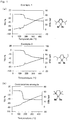
Fig. 1 shows a TG-DTA curve of a platinum complex in a first embodiment. -
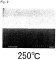
Fig. 2 shows a cross-sectional photograph of a platinum thin film in the first embodiment. -
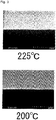
Fig. 3 shows a cross-sectional photograph of a platinum thin film in a second embodiment. -
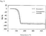
Fig. 4 shows a TG curve of a platinum complex in a third embodiment. - Hereinafter, the best embodiment in the present invention will be described.
- In the present embodiment, three kinds of platinum complexes as described below were synthesized. For the synthesized platinum complexes, physical properties were evaluated and film formation test was performed as a raw material for chemical deposition.
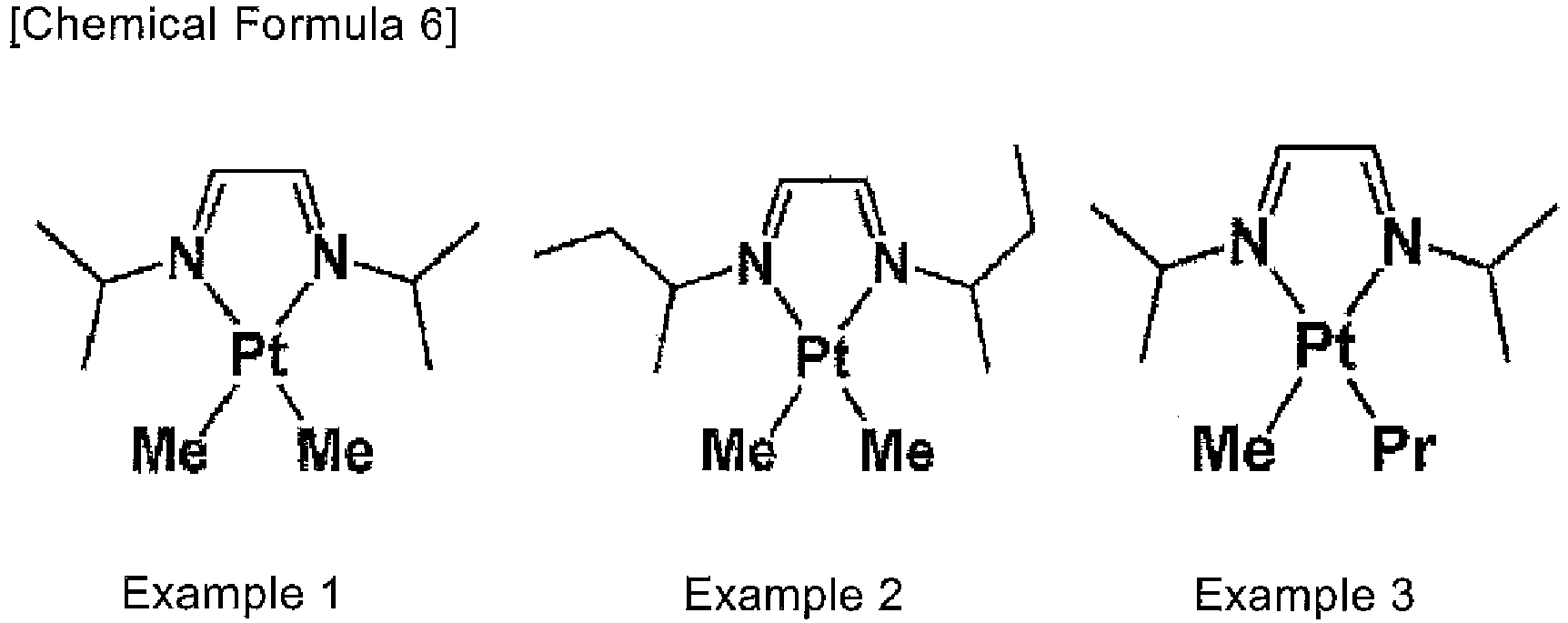
- (N,N'-diisopropyl-1,4-diazabutadiene)dimethylplatinum) that was a platinum complex in which diazabutadiene having two iso-propyl groups bonded to two imines and two methyl groups as alkyl anions were coordinated (each of substituents R1 and R4 was an iso-propyl group, each of R2 and R3 was a hydrogen atom, and each of R5 and R6 was a methyl group). The formula of the synthesis reaction is as follows. Hereinafter, the manufacturing process will be described in detail.


- Each of 1.4 g (10 mmol) of N,N'-diisopropyl-1,4-diazabutadiene and 1.55 g (5.0 mmol) of (1,4-hexadiene)dimethylplatinum was added in this order into a flask containing 75 ml of hexane and, after that, the mixture was stirred for 18 hours at room temperature. After the end of the reaction, the reaction product was concentrated to give a magenta solid. The obtained solid was sublimated and purified to give 1.45 g (4.0 mmol) of (N,N'-diisopropyl-1,4-diazabutadiene)dimethylplatinum that was a target (yield: 79%, melting point: 110°C).
- (N,N'-di-sec-butyl-1,4-diazabutadiene)dimethylplatinum) that was a platinum complex in which diazabutadiene having two sec-butyl groups bonded to two imines and two methyl groups as alkyl anions were coordinated (each of substituents R1 and R4 was a sec-butyl group, each of R2 and R3 was a hydrogen atom, and each of R5 and R6 was a methyl group). The formula of the synthesis reaction is as follows. Hereinafter, the manufacturing process will be described in detail.

- Each of 1.7 g (10 mmol) of N,N'-di-sec-butyl-1,4-diazabutadiene and 1.55 g (5.0 mmol) of (1,4-hexadiene)dimethylplatinum was added in this order into a flask containing 75 ml of hexane and, after that, the mixture was stirred for 18 hours at room temperature. After the reaction was completed, the reaction product was concentrated to give a magenta liquid. The obtained liquid was distilled and purified to give 1.77 g (4.5 mmol) of (N,N'-di-sec-butyl-1,4-diazabutadiene)dimethylplatinum that was a target (yield: 89%).
- (N,N'-diisopropyl-1,4-diazabutadiene)(methyl)(propyl)platinum that was a platinum complex in which diazabutadiene having two iso-propyl groups bonded to two imines and a methyl group and an n-propyl group as alkyl anions were coordinated (each of substituents R1 and R4 was an iso-propyl group, each of R2 and R3 was a hydrogen atom, R5 was a methyl group, and R6 was an n-propyl group). The formula of the synthesis reaction is as follows. Hereinafter, the manufacturing process will be described in detail.

- Each of 1.4 g (10 mmol) of N,N'-diisopropyl-1,4-diazabutadiene and 1.81 g (5.0 mmol) of (1,5-cyclooctadiene)(methyl)(propyl)platinum was added in this order into a flask containing 75 ml of hexane and, after that, the mixture was fluxed for 18 hours: After the end of the reaction, the reaction product was concentrated and purified to give 0.2 g (0.5 mmol) of (N,N'-diisopropyl-1,4-diazabutadiene)(methyl)(propyl)platinum that was a target in a state of a magenta liquid (yield: 10%).
- Evaluation of physical properties of platinum complex: Physical properties of platinum complexes in Examples 1 and 2 were evaluated by TG-DTA. In the analysis, changes in heat quantity and weight of a sample were observed when a platinum complex sample (5 mg) was heated from room temperature to 450°C that was a range of measurement temperature at a temperature rising rate of 5 °C/min under a nitrogen atmosphere with TG-DTA2000SA manufactured by BRUKER Corporation. Results are shown in
Fig. 1(a) . Further, there are shown results of TG-DTA analysis that was performed in the same way as above using dimethyl(N,N,N',N'-tetramethylethylenediamine)platinum not having conjugated diene as Comparative Example (Fig. 1(b) ). - From the results of DTA in
Fig. 1 , there was seen from (a) a build up of an exothermic peak that was convex upward near 160°C in complexes in Examples 1 and 2 in which the diimine was coordinated. In contrast, there was seen from (b) a build up of an exothermic peak near 125°C in a complex in which diamine was coordinated. The exothermic peak suggests generation of decomposition of a compound. Accordingly, the complexes in Examples 1 and 2 (diimine was coordinated) had a decomposition temperature that was higher in around 35°C and had a higher thermal stability as compared with the complex in which diamine was coordinated. From the viewpoint, the compound in Comparative Example decomposes and cannot be purified when a sublimation experiment (30 Pa, 110 to 120°C) is performed but, in contrast, the compound in Example 1 is not decomposed and can be purified. Meanwhile, a difference occurs between results of the sublimation experiment and the evaluation by TG-DTA because conditions such as presence/absence of measurement temperature rising are different. - Film formation test: Next, film formation tests of platinum thin films were performed by a CVD method with platinum complexes in Examples 1 to 3 used as raw compounds.
- A platinum thin film was deposited on a silicon substrate (15 mm × 15 mm). A thermal CVD apparatus of a hot wall type was used as a deposition apparatus. A reaction gas (hydrogen) was flown at a constant flow rate using a mass flow controller. Film formation conditions are as follows. Further, specific resistance of the thin film was measured by a four-probe method. The result of SEM observation of the formed platinum thin film is shown in
Fig. 2 . -
- Substrate: Si
- Film formation temperature: 250°C
- Sample temperature: 105°C
- Film formation pressure: 5 torr
- Flow rate of reaction gas (hydrogen): 10 sccm
- Film formation time: 10 minutes
- As the results of the above film formation tests, the platinum thin film was able to be deposited and the formed thin film had a smooth and uniform surface in all cases where any complex in Examples 1 to 3 was used as a raw material. Film thickness and specific resistance were measured for the platinum thin film that was formed in Example 1, and the Pt film had a sufficient thickness of 6.5 nm and a low specific resistance of 77.2 µΩ·cm. Further, the formation of a platinum thin film having a smooth and uniform surface was confirmed also by the SEM photograph in
Fig. 2 . - In the present embodiment, film formation tests onto respective Si substrates in the first embodiment were performed at film formation temperatures of 200°C and 225°C to evaluate low-temperature film formation properties. Other film formation conditions were the same as the conditions in the first embodiment. Results are shown in Table below. The deposition results in the first embodiment are shown together in the Table below. Further, a SEM-observed result of the formed platinum thin film is shown in
Fig. 3 .[Table 1] Film formation temperature (°C) Pt film thickness (nm) Specific resistance (µΩ·cm) 200 4.5 85.8 225 6.5 97.8 250 6.5 77.2 - Platinum thin films that were formed at 200°C or 225°C in film formation temperature also had a smooth and uniform surface from SEM photographs in
Fig. 3 . Further, the Pt film thickness and the specific resistance were almost equivalent to those in the case when a film was formed at 250°C in film formation temperature as shown in above Table. - In the present embodiment, dimethyl(N,N,N',N'-tetramethylethylenediamine)platinium was used as Comparative Example relative to Example and thermal stability and deposition properties were evaluated.
- Reduced pressure TG measurement (vaporization properties): A platinum complex sample (5 mg) was heated and analyzed with TG-DTA2000SA manufactured by BRUKER Corporation in a measurement temperature range of room temperature to 450°C at temperature rising rate of 5 °C/min and pressure of 5 torr under a nitrogen atmosphere. Results are shown in
Fig. 4 . - From the result of TG measurement, it was shown that the complex having diamine in Comparative Example generated about 15% of residue, and that the complex having the diimine in Example 1 generated around 10% of residue and had high thermal stability and high sublimation efficiency irrespective of high vaporization initiation temperature, from
Fig. 4 . It is considered that the complex having diamine in Comparative Example had low vapor pressure and generated thermal decomposition prior to vaporization in the temperature rising process. - Film formation test: A Pt thin film was formed on a substrate Si at 200°C in film formation temperature using the platinum complex in Example or in Comparative Example as a raw material for chemical deposition. In Comparative Example, sample temperature was set to be 110°C. Other film formation conditions were set to be the same as conditions in the first embodiment.
- As the results of film formation tests, a platinum thin film was formed even at 200°C in film formation temperature in the case of the complex in Example 1 but, in contrast, a film was not able to be formed in the case of the complex in Comparative Example because decomposition of the compound occurred in vaporization of the sample.
- From the above, it was confirmed that the complex in Example 1 had both vaporization properties and film formation properties suitable for the formation of a platinum thin film.
- The present inventive raw material has high vapor pressure and is capable of forming a highly accurate platinum thin film at low temperature and also has moderate thermal stability to exert excellent handling properties. Consequently, the raw material is useful for the film formation onto a steric structure and can be applied to a stereoscopic electrode having a three-dimensional structure of a field-effect transistor (FET), and the like.
Claims (7)
- A raw material for chemical deposition for manufacturing a platinum thin film or a platinum compound thin film by a chemical deposition method, the raw material comprising
an organoplatinum compound in which diimine containing two imines and alkyl anions are coordinated to a divalent platinum as shown by a formula below:
- The raw material for chemical deposition according to claim 1, wherein each of R1 and R4 represents any one of a hydrogen atom, a methyl group, an ethyl group, a propyl group and a butyl group.
- The raw material for chemical deposition according to claim 1 or 2,
wherein each of R1 and R4 represents any one of an iso-propyl group, a sec-butyl group and a tert-butyl group. - The raw material for chemical deposition according to any of claims 1 to 3,
wherein each of R2 and R3 represents a hydrogen atom or a methyl group. - The raw material for chemical deposition according to any of claims 1 to 4,
wherein a total carbon number obtained by summing up all carbon numbers of substituents R1 to R4 is 12 or less. - The raw material for chemical deposition according to any of claims 1 to 5,
wherein each of R5 and R6 represents any one of a methyl group, an ethyl group and an n-propyl group. - A chemical deposition method of a platinum thin film or a platinum compound thin film, comprising: vaporizing a raw material composed of an organoplatinum compound to form a raw material gas, and heating the raw material gas while introducing the raw material gas onto a substrate surface,
wherein the raw material for chemical deposition defined in any of claims 1 to 6 is used as the raw material.
Applications Claiming Priority (2)
| Application Number | Priority Date | Filing Date | Title |
|---|---|---|---|
| JP2015096976A JP5952460B1 (en) | 2015-05-12 | 2015-05-12 | Chemical vapor deposition material comprising an organic platinum compound and chemical vapor deposition method using the chemical vapor deposition material |
| PCT/JP2016/063693 WO2016181916A1 (en) | 2015-05-12 | 2016-05-09 | Chemical vapor deposition starting material comprising organic platinum compound, and chemical vapor deposition method using said chemical vapor deposition starting material |
Publications (2)
| Publication Number | Publication Date |
|---|---|
| EP3299490A4 EP3299490A4 (en) | 2018-03-28 |
| EP3299490A1 true EP3299490A1 (en) | 2018-03-28 |
Family
ID=56375097
Family Applications (1)
| Application Number | Title | Priority Date | Filing Date |
|---|---|---|---|
| EP16792641.9A Withdrawn EP3299490A1 (en) | 2015-05-12 | 2016-05-09 | Chemical vapor deposition starting material comprising organic platinum compound, and chemical vapor deposition method using said chemical vapor deposition starting material |
Country Status (6)
| Country | Link |
|---|---|
| US (1) | US10077282B2 (en) |
| EP (1) | EP3299490A1 (en) |
| JP (1) | JP5952460B1 (en) |
| KR (1) | KR102041027B1 (en) |
| TW (1) | TWI638901B (en) |
| WO (1) | WO2016181916A1 (en) |
Family Cites Families (11)
| Publication number | Priority date | Publication date | Assignee | Title |
|---|---|---|---|---|
| JP2615414B2 (en) * | 1994-02-25 | 1997-05-28 | 工業技術院長 | Information recording material |
| KR100277569B1 (en) * | 1994-12-27 | 2001-03-02 | 후지무라 마사지카, 아키모토 유미 | Composition for forming electrode pattern and method of forming electrode pattern |
| US5783716A (en) | 1996-06-28 | 1998-07-21 | Advanced Technology Materials, Inc. | Platinum source compositions for chemical vapor deposition of platinum |
| JP3379315B2 (en) * | 1995-12-11 | 2003-02-24 | 三菱マテリアル株式会社 | Raw materials for forming platinum thin films by metal organic chemical vapor deposition |
| JP3321729B2 (en) | 1998-04-03 | 2002-09-09 | 株式会社高純度化学研究所 | Trimethyl (ethylcyclopentadienyl) platinum, method for producing the same, and method for producing platinum-containing thin film using the same |
| DE10358665A1 (en) * | 2003-12-12 | 2005-07-07 | Basf Ag | Use of platinum (II) complexes as luminescent materials in organic light-emitting diodes (OLEDs) |
| US7439338B2 (en) | 2005-06-28 | 2008-10-21 | Micron Technology, Inc. | Beta-diketiminate ligand sources and metal-containing compounds thereof, and systems and methods including same |
| US7776394B2 (en) * | 2005-08-08 | 2010-08-17 | E.I. Du Pont De Nemours And Company | Atomic layer deposition of metal-containing films using surface-activating agents |
| WO2012144455A1 (en) | 2011-04-20 | 2012-10-26 | 田中貴金属工業株式会社 | Organic platinum compound for chemical vapor deposition, and chemical vapor deposition method using organic platinum compound |
| JP5156120B1 (en) * | 2011-10-14 | 2013-03-06 | 田中貴金属工業株式会社 | Chemical vapor deposition material comprising an organic platinum compound and chemical vapor deposition method using the chemical vapor deposition material |
| JP2013184925A (en) * | 2012-03-08 | 2013-09-19 | Osaka Univ | Tungsten complex, catalyst for metathesis reaction and production method of cyclic olefin ring-opened polymer |
-
2015
- 2015-05-12 JP JP2015096976A patent/JP5952460B1/en active Active
-
2016
- 2016-05-04 TW TW105113840A patent/TWI638901B/en active
- 2016-05-09 KR KR1020177027929A patent/KR102041027B1/en active Active
- 2016-05-09 WO PCT/JP2016/063693 patent/WO2016181916A1/en not_active Ceased
- 2016-05-09 EP EP16792641.9A patent/EP3299490A1/en not_active Withdrawn
- 2016-05-09 US US15/558,262 patent/US10077282B2/en active Active
Also Published As
| Publication number | Publication date |
|---|---|
| US10077282B2 (en) | 2018-09-18 |
| KR102041027B1 (en) | 2019-11-05 |
| TW201708591A (en) | 2017-03-01 |
| EP3299490A4 (en) | 2018-03-28 |
| US20180072765A1 (en) | 2018-03-15 |
| WO2016181916A1 (en) | 2016-11-17 |
| TWI638901B (en) | 2018-10-21 |
| KR20170127499A (en) | 2017-11-21 |
| JP5952460B1 (en) | 2016-07-13 |
| JP2016210741A (en) | 2016-12-15 |
Similar Documents
| Publication | Publication Date | Title |
|---|---|---|
| EP3348667A1 (en) | Chemical vapor deposition feedstock comprising organic ruthenium compound and chemical vapor deposition method using said chemical vapor deposition feedstock | |
| US10815260B2 (en) | Chemical vapor deposition raw material including dinuclear ruthenium complex and chemical deposition method using chemical vapor deposition raw material | |
| EP3296425A1 (en) | Chemical vapor deposition starting material comprising organic platinum compound, and chemical vapor deposition method using said chemical vapor deposition starting material | |
| US8911827B2 (en) | Chemical vapor deposition method using an organoplatinum compound | |
| US10131987B2 (en) | Raw material for chemical deposition including organoruthenium compound, and chemical deposition method using the raw material for chemical deposition | |
| EP3299490A1 (en) | Chemical vapor deposition starting material comprising organic platinum compound, and chemical vapor deposition method using said chemical vapor deposition starting material | |
| KR102351888B1 (en) | A raw material for vapor deposition containing an organic platinum compound and a vapor deposition method using the raw material for vapor deposition |
Legal Events
| Date | Code | Title | Description |
|---|---|---|---|
| PUAI | Public reference made under article 153(3) epc to a published international application that has entered the european phase |
Free format text: ORIGINAL CODE: 0009012 |
|
| 17P | Request for examination filed |
Effective date: 20171201 |
|
| A4 | Supplementary search report drawn up and despatched |
Effective date: 20180223 |
|
| AK | Designated contracting states |
Kind code of ref document: A1 Designated state(s): AL AT BE BG CH CY CZ DE DK EE ES FI FR GB GR HR HU IE IS IT LI LT LU LV MC MK MT NL NO PL PT RO RS SE SI SK SM TR |
|
| AX | Request for extension of the european patent |
Extension state: BA ME |
|
| DAV | Request for validation of the european patent (deleted) | ||
| DAX | Request for extension of the european patent (deleted) | ||
| STAA | Information on the status of an ep patent application or granted ep patent |
Free format text: STATUS: THE APPLICATION HAS BEEN WITHDRAWN |
|
| 18W | Application withdrawn |
Effective date: 20190227 |